JP2011522423A - Photovoltaic conductor: A composition containing submicron particles - Google Patents
Photovoltaic conductor: A composition containing submicron particles Download PDFInfo
- Publication number
- JP2011522423A JP2011522423A JP2011511805A JP2011511805A JP2011522423A JP 2011522423 A JP2011522423 A JP 2011522423A JP 2011511805 A JP2011511805 A JP 2011511805A JP 2011511805 A JP2011511805 A JP 2011511805A JP 2011522423 A JP2011522423 A JP 2011522423A
- Authority
- JP
- Japan
- Prior art keywords
- composition
- submicron particles
- thick film
- microns
- inorganic
- Prior art date
- Legal status (The legal status is an assumption and is not a legal conclusion. Google has not performed a legal analysis and makes no representation as to the accuracy of the status listed.)
- Withdrawn
Links
- 239000000203 mixture Substances 0.000 title claims abstract description 132
- 239000002245 particle Substances 0.000 title claims description 67
- 239000004020 conductor Substances 0.000 title claims description 27
- 239000004065 semiconductor Substances 0.000 claims abstract description 56
- 229910052709 silver Inorganic materials 0.000 claims description 32
- 239000000758 substrate Substances 0.000 claims description 32
- 239000004332 silver Substances 0.000 claims description 29
- 238000000034 method Methods 0.000 claims description 25
- 238000010304 firing Methods 0.000 claims description 23
- XLOMVQKBTHCTTD-UHFFFAOYSA-N Zinc monoxide Chemical compound [Zn]=O XLOMVQKBTHCTTD-UHFFFAOYSA-N 0.000 claims description 22
- 239000000654 additive Substances 0.000 claims description 21
- 229910044991 metal oxide Inorganic materials 0.000 claims description 11
- 150000004706 metal oxides Chemical class 0.000 claims description 11
- 229910052802 copper Inorganic materials 0.000 claims description 10
- 229910052751 metal Inorganic materials 0.000 claims description 10
- 239000002184 metal Substances 0.000 claims description 10
- VYPSYNLAJGMNEJ-UHFFFAOYSA-N Silicium dioxide Chemical compound O=[Si]=O VYPSYNLAJGMNEJ-UHFFFAOYSA-N 0.000 claims description 9
- 229910052814 silicon oxide Inorganic materials 0.000 claims description 9
- HQVNEWCFYHHQES-UHFFFAOYSA-N silicon nitride Chemical compound N12[Si]34N5[Si]62N3[Si]51N64 HQVNEWCFYHHQES-UHFFFAOYSA-N 0.000 claims description 8
- 229910052581 Si3N4 Inorganic materials 0.000 claims description 7
- GWEVSGVZZGPLCZ-UHFFFAOYSA-N Titan oxide Chemical compound O=[Ti]=O GWEVSGVZZGPLCZ-UHFFFAOYSA-N 0.000 claims description 7
- 150000001875 compounds Chemical class 0.000 claims description 7
- OGIDPMRJRNCKJF-UHFFFAOYSA-N titanium oxide Inorganic materials [Ti]=O OGIDPMRJRNCKJF-UHFFFAOYSA-N 0.000 claims description 7
- 229910052684 Cerium Inorganic materials 0.000 claims description 6
- 229910052804 chromium Inorganic materials 0.000 claims description 6
- 229910052742 iron Inorganic materials 0.000 claims description 6
- 229910052745 lead Inorganic materials 0.000 claims description 6
- 229910052748 manganese Inorganic materials 0.000 claims description 6
- 229910052707 ruthenium Inorganic materials 0.000 claims description 6
- 229910052718 tin Inorganic materials 0.000 claims description 6
- 229910052719 titanium Inorganic materials 0.000 claims description 6
- 239000010936 titanium Substances 0.000 claims description 6
- 229910052725 zinc Inorganic materials 0.000 claims description 6
- 229910052726 zirconium Inorganic materials 0.000 claims description 6
- 239000011230 binding agent Substances 0.000 claims description 5
- 238000009826 distribution Methods 0.000 claims description 4
- 150000002739 metals Chemical class 0.000 claims description 4
- 229910004205 SiNX Inorganic materials 0.000 claims description 2
- 230000002902 bimodal effect Effects 0.000 claims description 2
- XUIMIQQOPSSXEZ-UHFFFAOYSA-N Silicon Chemical compound [Si] XUIMIQQOPSSXEZ-UHFFFAOYSA-N 0.000 abstract description 9
- 229910052710 silicon Inorganic materials 0.000 abstract description 9
- 239000010703 silicon Substances 0.000 abstract description 9
- BQCADISMDOOEFD-UHFFFAOYSA-N Silver Chemical compound [Ag] BQCADISMDOOEFD-UHFFFAOYSA-N 0.000 description 29
- 239000011521 glass Substances 0.000 description 17
- 229910052782 aluminium Inorganic materials 0.000 description 13
- 239000011701 zinc Substances 0.000 description 13
- 230000000996 additive effect Effects 0.000 description 11
- XAGFODPZIPBFFR-UHFFFAOYSA-N aluminium Chemical compound [Al] XAGFODPZIPBFFR-UHFFFAOYSA-N 0.000 description 10
- 239000011787 zinc oxide Substances 0.000 description 10
- 239000010949 copper Substances 0.000 description 8
- 238000004519 manufacturing process Methods 0.000 description 8
- 239000000843 powder Substances 0.000 description 8
- 238000007639 printing Methods 0.000 description 7
- 238000012360 testing method Methods 0.000 description 6
- 239000000463 material Substances 0.000 description 5
- 229920000642 polymer Polymers 0.000 description 5
- 239000007787 solid Substances 0.000 description 5
- 239000006117 anti-reflective coating Substances 0.000 description 4
- IPCSVZSSVZVIGE-UHFFFAOYSA-N hexadecanoic acid Chemical compound CCCCCCCCCCCCCCCC(O)=O IPCSVZSSVZVIGE-UHFFFAOYSA-N 0.000 description 4
- 229910052763 palladium Inorganic materials 0.000 description 4
- 238000000623 plasma-assisted chemical vapour deposition Methods 0.000 description 4
- 239000002904 solvent Substances 0.000 description 4
- 239000004094 surface-active agent Substances 0.000 description 4
- YCKRFDGAMUMZLT-UHFFFAOYSA-N Fluorine atom Chemical compound [F] YCKRFDGAMUMZLT-UHFFFAOYSA-N 0.000 description 3
- 239000004110 Zinc silicate Substances 0.000 description 3
- 239000006185 dispersion Substances 0.000 description 3
- 238000001035 drying Methods 0.000 description 3
- 229910052731 fluorine Inorganic materials 0.000 description 3
- 239000011737 fluorine Substances 0.000 description 3
- 229910052737 gold Inorganic materials 0.000 description 3
- QIQXTHQIDYTFRH-UHFFFAOYSA-N octadecanoic acid Chemical compound CCCCCCCCCCCCCCCCCC(O)=O QIQXTHQIDYTFRH-UHFFFAOYSA-N 0.000 description 3
- 238000005240 physical vapour deposition Methods 0.000 description 3
- 229910052697 platinum Inorganic materials 0.000 description 3
- -1 structures (eg Substances 0.000 description 3
- 235000012431 wafers Nutrition 0.000 description 3
- XSMMCTCMFDWXIX-UHFFFAOYSA-N zinc silicate Chemical compound [Zn+2].[O-][Si]([O-])=O XSMMCTCMFDWXIX-UHFFFAOYSA-N 0.000 description 3
- 235000019352 zinc silicate Nutrition 0.000 description 3
- SVTBMSDMJJWYQN-UHFFFAOYSA-N 2-methylpentane-2,4-diol Chemical compound CC(O)CC(C)(C)O SVTBMSDMJJWYQN-UHFFFAOYSA-N 0.000 description 2
- IJGRMHOSHXDMSA-UHFFFAOYSA-N Atomic nitrogen Chemical compound N#N IJGRMHOSHXDMSA-UHFFFAOYSA-N 0.000 description 2
- 239000001856 Ethyl cellulose Substances 0.000 description 2
- ZZSNKZQZMQGXPY-UHFFFAOYSA-N Ethyl cellulose Chemical compound CCOCC1OC(OC)C(OCC)C(OCC)C1OC1C(O)C(O)C(OC)C(CO)O1 ZZSNKZQZMQGXPY-UHFFFAOYSA-N 0.000 description 2
- 235000021314 Palmitic acid Nutrition 0.000 description 2
- 235000021355 Stearic acid Nutrition 0.000 description 2
- 150000001298 alcohols Chemical class 0.000 description 2
- 239000012298 atmosphere Substances 0.000 description 2
- QVGXLLKOCUKJST-UHFFFAOYSA-N atomic oxygen Chemical compound [O] QVGXLLKOCUKJST-UHFFFAOYSA-N 0.000 description 2
- 238000000576 coating method Methods 0.000 description 2
- GHVNFZFCNZKVNT-UHFFFAOYSA-N decanoic acid Chemical class CCCCCCCCCC(O)=O GHVNFZFCNZKVNT-UHFFFAOYSA-N 0.000 description 2
- DOIRQSBPFJWKBE-UHFFFAOYSA-N dibutyl phthalate Chemical compound CCCCOC(=O)C1=CC=CC=C1C(=O)OCCCC DOIRQSBPFJWKBE-UHFFFAOYSA-N 0.000 description 2
- POULHZVOKOAJMA-UHFFFAOYSA-N dodecanoic acid Chemical compound CCCCCCCCCCCC(O)=O POULHZVOKOAJMA-UHFFFAOYSA-N 0.000 description 2
- 229920001249 ethyl cellulose Polymers 0.000 description 2
- 235000019325 ethyl cellulose Nutrition 0.000 description 2
- 239000007788 liquid Substances 0.000 description 2
- WQEPLUUGTLDZJY-UHFFFAOYSA-N n-Pentadecanoic acid Natural products CCCCCCCCCCCCCCC(O)=O WQEPLUUGTLDZJY-UHFFFAOYSA-N 0.000 description 2
- OQCDKBAXFALNLD-UHFFFAOYSA-N octadecanoic acid Natural products CCCCCCCC(C)CCCCCCCCC(O)=O OQCDKBAXFALNLD-UHFFFAOYSA-N 0.000 description 2
- 239000001301 oxygen Substances 0.000 description 2
- 229910052760 oxygen Inorganic materials 0.000 description 2
- 150000003839 salts Chemical class 0.000 description 2
- 238000007650 screen-printing Methods 0.000 description 2
- 239000008117 stearic acid Substances 0.000 description 2
- 238000002230 thermal chemical vapour deposition Methods 0.000 description 2
- OYHQOLUKZRVURQ-NTGFUMLPSA-N (9Z,12Z)-9,10,12,13-tetratritiooctadeca-9,12-dienoic acid Chemical class C(CCCCCCC\C(=C(/C\C(=C(/CCCCC)\[3H])\[3H])\[3H])\[3H])(=O)O OYHQOLUKZRVURQ-NTGFUMLPSA-N 0.000 description 1
- WRIDQFICGBMAFQ-UHFFFAOYSA-N (E)-8-Octadecenoic acid Natural products CCCCCCCCCC=CCCCCCCC(O)=O WRIDQFICGBMAFQ-UHFFFAOYSA-N 0.000 description 1
- WUOACPNHFRMFPN-SECBINFHSA-N (S)-(-)-alpha-terpineol Chemical compound CC1=CC[C@@H](C(C)(C)O)CC1 WUOACPNHFRMFPN-SECBINFHSA-N 0.000 description 1
- RUJPNZNXGCHGID-UHFFFAOYSA-N (Z)-beta-Terpineol Natural products CC(=C)C1CCC(C)(O)CC1 RUJPNZNXGCHGID-UHFFFAOYSA-N 0.000 description 1
- DURPTKYDGMDSBL-UHFFFAOYSA-N 1-butoxybutane Chemical compound CCCCOCCCC DURPTKYDGMDSBL-UHFFFAOYSA-N 0.000 description 1
- OAYXUHPQHDHDDZ-UHFFFAOYSA-N 2-(2-butoxyethoxy)ethanol Chemical compound CCCCOCCOCCO OAYXUHPQHDHDDZ-UHFFFAOYSA-N 0.000 description 1
- VXQBJTKSVGFQOL-UHFFFAOYSA-N 2-(2-butoxyethoxy)ethyl acetate Chemical compound CCCCOCCOCCOC(C)=O VXQBJTKSVGFQOL-UHFFFAOYSA-N 0.000 description 1
- TWJNQYPJQDRXPH-UHFFFAOYSA-N 2-cyanobenzohydrazide Chemical class NNC(=O)C1=CC=CC=C1C#N TWJNQYPJQDRXPH-UHFFFAOYSA-N 0.000 description 1
- HXDLWJWIAHWIKI-UHFFFAOYSA-N 2-hydroxyethyl acetate Chemical compound CC(=O)OCCO HXDLWJWIAHWIKI-UHFFFAOYSA-N 0.000 description 1
- KXGFMDJXCMQABM-UHFFFAOYSA-N 2-methoxy-6-methylphenol Chemical compound [CH]OC1=CC=CC([CH])=C1O KXGFMDJXCMQABM-UHFFFAOYSA-N 0.000 description 1
- LQJBNNIYVWPHFW-UHFFFAOYSA-N 20:1omega9c fatty acid Natural products CCCCCCCCCCC=CCCCCCCCC(O)=O LQJBNNIYVWPHFW-UHFFFAOYSA-N 0.000 description 1
- QSBYPNXLFMSGKH-UHFFFAOYSA-N 9-Heptadecensaeure Natural products CCCCCCCC=CCCCCCCCC(O)=O QSBYPNXLFMSGKH-UHFFFAOYSA-N 0.000 description 1
- RSWGJHLUYNHPMX-UHFFFAOYSA-N Abietic-Saeure Natural products C12CCC(C(C)C)=CC2=CCC2C1(C)CCCC2(C)C(O)=O RSWGJHLUYNHPMX-UHFFFAOYSA-N 0.000 description 1
- 229910018072 Al 2 O 3 Inorganic materials 0.000 description 1
- 229910016569 AlF 3 Inorganic materials 0.000 description 1
- QGZKDVFQNNGYKY-UHFFFAOYSA-O Ammonium Chemical compound [NH4+] QGZKDVFQNNGYKY-UHFFFAOYSA-O 0.000 description 1
- ZOXJGFHDIHLPTG-UHFFFAOYSA-N Boron Chemical compound [B] ZOXJGFHDIHLPTG-UHFFFAOYSA-N 0.000 description 1
- 239000005632 Capric acid (CAS 334-48-5) Chemical class 0.000 description 1
- RYGMFSIKBFXOCR-UHFFFAOYSA-N Copper Chemical compound [Cu] RYGMFSIKBFXOCR-UHFFFAOYSA-N 0.000 description 1
- LFQSCWFLJHTTHZ-UHFFFAOYSA-N Ethanol Chemical compound CCO LFQSCWFLJHTTHZ-UHFFFAOYSA-N 0.000 description 1
- 229920000896 Ethulose Polymers 0.000 description 1
- 239000001859 Ethyl hydroxyethyl cellulose Substances 0.000 description 1
- DGAQECJNVWCQMB-PUAWFVPOSA-M Ilexoside XXIX Chemical compound C[C@@H]1CC[C@@]2(CC[C@@]3(C(=CC[C@H]4[C@]3(CC[C@@H]5[C@@]4(CC[C@@H](C5(C)C)OS(=O)(=O)[O-])C)C)[C@@H]2[C@]1(C)O)C)C(=O)O[C@H]6[C@@H]([C@H]([C@@H]([C@H](O6)CO)O)O)O.[Na+] DGAQECJNVWCQMB-PUAWFVPOSA-M 0.000 description 1
- 239000005639 Lauric acid Substances 0.000 description 1
- 235000021360 Myristic acid Nutrition 0.000 description 1
- TUNFSRHWOTWDNC-UHFFFAOYSA-N Myristic acid Chemical class CCCCCCCCCCCCCC(O)=O TUNFSRHWOTWDNC-UHFFFAOYSA-N 0.000 description 1
- 239000005642 Oleic acid Substances 0.000 description 1
- ZQPPMHVWECSIRJ-UHFFFAOYSA-N Oleic acid Natural products CCCCCCCCC=CCCCCCCCC(O)=O ZQPPMHVWECSIRJ-UHFFFAOYSA-N 0.000 description 1
- OAICVXFJPJFONN-UHFFFAOYSA-N Phosphorus Chemical compound [P] OAICVXFJPJFONN-UHFFFAOYSA-N 0.000 description 1
- ZLMJMSJWJFRBEC-UHFFFAOYSA-N Potassium Chemical compound [K] ZLMJMSJWJFRBEC-UHFFFAOYSA-N 0.000 description 1
- 229910018885 Pt—Au Inorganic materials 0.000 description 1
- KHPCPRHQVVSZAH-HUOMCSJISA-N Rosin Natural products O(C/C=C/c1ccccc1)[C@H]1[C@H](O)[C@@H](O)[C@@H](O)[C@@H](CO)O1 KHPCPRHQVVSZAH-HUOMCSJISA-N 0.000 description 1
- 229910004541 SiN Inorganic materials 0.000 description 1
- 229910004298 SiO 2 Inorganic materials 0.000 description 1
- 229910010413 TiO 2 Inorganic materials 0.000 description 1
- 229910045601 alloy Inorganic materials 0.000 description 1
- 239000000956 alloy Substances 0.000 description 1
- OVKDFILSBMEKLT-UHFFFAOYSA-N alpha-Terpineol Natural products CC(=C)C1(O)CCC(C)=CC1 OVKDFILSBMEKLT-UHFFFAOYSA-N 0.000 description 1
- 229910021417 amorphous silicon Inorganic materials 0.000 description 1
- 239000010953 base metal Substances 0.000 description 1
- 238000009835 boiling Methods 0.000 description 1
- 229910052796 boron Inorganic materials 0.000 description 1
- 239000005388 borosilicate glass Substances 0.000 description 1
- 239000002775 capsule Substances 0.000 description 1
- 239000000919 ceramic Substances 0.000 description 1
- 238000006243 chemical reaction Methods 0.000 description 1
- 239000011248 coating agent Substances 0.000 description 1
- DQUIAMCJEJUUJC-UHFFFAOYSA-N dibismuth;dioxido(oxo)silane Chemical compound [Bi+3].[Bi+3].[O-][Si]([O-])=O.[O-][Si]([O-])=O.[O-][Si]([O-])=O DQUIAMCJEJUUJC-UHFFFAOYSA-N 0.000 description 1
- 238000009792 diffusion process Methods 0.000 description 1
- 235000019326 ethyl hydroxyethyl cellulose Nutrition 0.000 description 1
- 238000011049 filling Methods 0.000 description 1
- 238000001914 filtration Methods 0.000 description 1
- 150000002222 fluorine compounds Chemical class 0.000 description 1
- 239000007789 gas Substances 0.000 description 1
- 239000002241 glass-ceramic Substances 0.000 description 1
- 229940051250 hexylene glycol Drugs 0.000 description 1
- 239000001257 hydrogen Substances 0.000 description 1
- 229910052739 hydrogen Inorganic materials 0.000 description 1
- 125000004435 hydrogen atom Chemical class [H]* 0.000 description 1
- 239000004615 ingredient Substances 0.000 description 1
- 150000002500 ions Chemical class 0.000 description 1
- QXJSBBXBKPUZAA-UHFFFAOYSA-N isooleic acid Natural products CCCCCCCC=CCCCCCCCCC(O)=O QXJSBBXBKPUZAA-UHFFFAOYSA-N 0.000 description 1
- 239000003350 kerosene Substances 0.000 description 1
- 238000004898 kneading Methods 0.000 description 1
- 239000008204 material by function Substances 0.000 description 1
- 239000000155 melt Substances 0.000 description 1
- 238000002156 mixing Methods 0.000 description 1
- 229910021421 monocrystalline silicon Inorganic materials 0.000 description 1
- 229910052757 nitrogen Inorganic materials 0.000 description 1
- ZQPPMHVWECSIRJ-KTKRTIGZSA-N oleic acid Chemical compound CCCCCCCC\C=C/CCCCCCCC(O)=O ZQPPMHVWECSIRJ-KTKRTIGZSA-N 0.000 description 1
- 239000003960 organic solvent Substances 0.000 description 1
- 230000003647 oxidation Effects 0.000 description 1
- 238000007254 oxidation reaction Methods 0.000 description 1
- 150000002942 palmitic acid derivatives Chemical class 0.000 description 1
- 238000002161 passivation Methods 0.000 description 1
- 239000005011 phenolic resin Substances 0.000 description 1
- 229920001568 phenolic resin Polymers 0.000 description 1
- 229910052698 phosphorus Inorganic materials 0.000 description 1
- 239000011574 phosphorus Substances 0.000 description 1
- 238000005268 plasma chemical vapour deposition Methods 0.000 description 1
- 229910021420 polycrystalline silicon Inorganic materials 0.000 description 1
- 229920000193 polymethacrylate Polymers 0.000 description 1
- 239000011591 potassium Substances 0.000 description 1
- 229910052700 potassium Inorganic materials 0.000 description 1
- 230000005855 radiation Effects 0.000 description 1
- 239000012779 reinforcing material Substances 0.000 description 1
- 238000005245 sintering Methods 0.000 description 1
- 239000011734 sodium Substances 0.000 description 1
- 229910052708 sodium Inorganic materials 0.000 description 1
- 239000007962 solid dispersion Substances 0.000 description 1
- 239000007921 spray Substances 0.000 description 1
- 239000003381 stabilizer Substances 0.000 description 1
- QJVXKWHHAMZTBY-GCPOEHJPSA-N syringin Chemical compound COC1=CC(\C=C\CO)=CC(OC)=C1O[C@H]1[C@H](O)[C@@H](O)[C@H](O)[C@@H](CO)O1 QJVXKWHHAMZTBY-GCPOEHJPSA-N 0.000 description 1
- 235000012976 tarts Nutrition 0.000 description 1
- 150000003505 terpenes Chemical class 0.000 description 1
- 235000007586 terpenes Nutrition 0.000 description 1
- 239000002562 thickening agent Substances 0.000 description 1
- KHPCPRHQVVSZAH-UHFFFAOYSA-N trans-cinnamyl beta-D-glucopyranoside Natural products OC1C(O)C(O)C(CO)OC1OCC=CC1=CC=CC=C1 KHPCPRHQVVSZAH-UHFFFAOYSA-N 0.000 description 1
- 239000011345 viscous material Substances 0.000 description 1
- 239000002023 wood Substances 0.000 description 1
Images


Classifications
-
- H—ELECTRICITY
- H01—ELECTRIC ELEMENTS
- H01B—CABLES; CONDUCTORS; INSULATORS; SELECTION OF MATERIALS FOR THEIR CONDUCTIVE, INSULATING OR DIELECTRIC PROPERTIES
- H01B1/00—Conductors or conductive bodies characterised by the conductive materials; Selection of materials as conductors
- H01B1/14—Conductive material dispersed in non-conductive inorganic material
- H01B1/16—Conductive material dispersed in non-conductive inorganic material the conductive material comprising metals or alloys
-
- H—ELECTRICITY
- H01—ELECTRIC ELEMENTS
- H01B—CABLES; CONDUCTORS; INSULATORS; SELECTION OF MATERIALS FOR THEIR CONDUCTIVE, INSULATING OR DIELECTRIC PROPERTIES
- H01B1/00—Conductors or conductive bodies characterised by the conductive materials; Selection of materials as conductors
- H01B1/20—Conductive material dispersed in non-conductive organic material
- H01B1/22—Conductive material dispersed in non-conductive organic material the conductive material comprising metals or alloys
-
- H—ELECTRICITY
- H01—ELECTRIC ELEMENTS
- H01L—SEMICONDUCTOR DEVICES NOT COVERED BY CLASS H10
- H01L31/00—Semiconductor devices sensitive to infrared radiation, light, electromagnetic radiation of shorter wavelength or corpuscular radiation and specially adapted either for the conversion of the energy of such radiation into electrical energy or for the control of electrical energy by such radiation; Processes or apparatus specially adapted for the manufacture or treatment thereof or of parts thereof; Details thereof
- H01L31/02—Details
- H01L31/0224—Electrodes
- H01L31/022408—Electrodes for devices characterised by at least one potential jump barrier or surface barrier
- H01L31/022425—Electrodes for devices characterised by at least one potential jump barrier or surface barrier for solar cells
-
- Y—GENERAL TAGGING OF NEW TECHNOLOGICAL DEVELOPMENTS; GENERAL TAGGING OF CROSS-SECTIONAL TECHNOLOGIES SPANNING OVER SEVERAL SECTIONS OF THE IPC; TECHNICAL SUBJECTS COVERED BY FORMER USPC CROSS-REFERENCE ART COLLECTIONS [XRACs] AND DIGESTS
- Y02—TECHNOLOGIES OR APPLICATIONS FOR MITIGATION OR ADAPTATION AGAINST CLIMATE CHANGE
- Y02E—REDUCTION OF GREENHOUSE GAS [GHG] EMISSIONS, RELATED TO ENERGY GENERATION, TRANSMISSION OR DISTRIBUTION
- Y02E10/00—Energy generation through renewable energy sources
- Y02E10/50—Photovoltaic [PV] energy
Abstract
本発明の実施形態は、太陽電池装置で使用されるシリコン半導体装置と伝導性厚膜組成物とに関する。 Embodiments of the present invention relate to a silicon semiconductor device and a conductive thick film composition used in a solar cell device.
Description
本発明の実施形態は、太陽電池装置で使用されるシリコン半導体装置と導電性厚膜組成物とに関する。 Embodiments described herein relate generally to a silicon semiconductor device and a conductive thick film composition used in a solar cell device.
p型基部を有する従来の太陽電池構造は、電池の前面側(太陽側または照射側とも呼ばれる)にあってよい負極と、反対側にあってよい正極とを有する。半導体本体のpn接合にかかる適切な波長の放射は、本体内に正孔−電子対を発生するための外部エネルギー源として働く。pn接合に存在する電位差のために、正孔と電子は互いに反対方向に接合を横断し、これにより外部回路に電力を供給可能な電流の流れを生じさせる。ほとんどの太陽電池は金属化された(すなわち導電性金属接触を備える)シリコンウェーハの形式をとる。 A conventional solar cell structure having a p-type base has a negative electrode that may be on the front side of the battery (also referred to as the solar side or the irradiation side) and a positive electrode that may be on the opposite side. The appropriate wavelength of radiation on the pn junction of the semiconductor body serves as an external energy source for generating hole-electron pairs in the body. Due to the potential difference present at the pn junction, the holes and electrons traverse the junction in opposite directions, thereby creating a current flow that can supply power to the external circuit. Most solar cells take the form of metallized (ie with conductive metal contacts) silicon wafers.
電気的性能を改善した組成物、構造(例えば、半導体、太陽電池、またはフォトダイオード構造)、半導体装置(例えば、半導体、太陽電池、またはフォトダイオード装置)と、その製造方法の要求がある。 There is a need for compositions, structures (eg, semiconductors, solar cells, or photodiode structures) with improved electrical performance, semiconductor devices (eg, semiconductors, solar cells, or photodiode devices), and methods of manufacturing the same.
本発明の実施形態は、(a)1つまたは複数の導電性材料、(b)1つまたは複数の無機結合剤、(c)無機成分の1〜15%がサブミクロン粒子である有機ビヒクル、を含む組成物に関する。一実施形態では、無機成分の85〜99%が1.5〜10ミクロンの平均粒径d50を有することができる。一実施形態では、1つまたは複数の導電性材料は銀を含んでよい。一実施形態では、銀の一部はサブミクロン粒子を含む。一実施形態では、サブミクロン粒子は0.1〜1ミクロンの平均粒径d50を有する。一実施形態では、サブミクロン粒子は0.1〜0.6ミクロンの平均粒径d50を有する。一実施形態では、粒子は双峰粒度分布を有する。 Embodiments of the invention include (a) one or more conductive materials, (b) one or more inorganic binders, (c) an organic vehicle in which 1-15% of the inorganic components are submicron particles, It relates to the composition containing this. In one embodiment, 85-99% of the inorganic components can have an average particle size d50 of 1.5-10 microns. In one embodiment, the one or more conductive materials may include silver. In one embodiment, the portion of silver includes submicron particles. In one embodiment, the submicron particles have an average particle size d50 of 0.1 to 1 micron. In one embodiment, the submicron particles have an average particle size d50 of 0.1 to 0.6 microns. In one embodiment, the particles have a bimodal particle size distribution.
組成物は、(a)Zn、Pb、Bi、Gd、Ce、Zr、Ti、Mn、Sn、Ru、Co、Fe、Cu、Crから選択される金属、(b)Zn、Pb、Bi、Gd、Ce、Zr、Ti、Mn、Sn、Ru、Co、Fe、Cu、Crから選択される1つまたは複数の金属の金属酸化物、(c)焼成されると(b)の金属酸化物を生成可能な任意の化合物、(d)それらの混合物、からなる群から選択される1つまたは複数の添加剤を含んでよい。一実施形態では、添加剤はZnO、または焼成されるとZnOを形成する化合物を含んでよい。一実施形態では、ZnOおよび/または無機結合剤はサブミクロン粒子を含んでよい。ZnOは全組成の2〜10wt%であってよい。ガラスフリットは全組成の1〜6wt%であってよい。導電性材料はAgを含んでよい。Agは組成物中の固体の90〜99wt%であってよい。一実施形態では、無機成分は全組成の70〜95wt%であってよい。 The composition comprises: (a) a metal selected from Zn, Pb, Bi, Gd, Ce, Zr, Ti, Mn, Sn, Ru, Co, Fe, Cu, Cr; (b) Zn, Pb, Bi, Gd A metal oxide of one or more metals selected from Ce, Zr, Ti, Mn, Sn, Ru, Co, Fe, Cu, Cr, and (c) a metal oxide of (b) when fired. One or more additives selected from the group consisting of any compound that can be produced, (d) mixtures thereof, may be included. In one embodiment, the additive may include ZnO or a compound that forms ZnO when fired. In one embodiment, the ZnO and / or inorganic binder may include submicron particles. ZnO may be 2-10 wt% of the total composition. The glass frit may be 1-6 wt% of the total composition. The conductive material may include Ag. Ag may be 90-99 wt% of the solids in the composition. In one embodiment, the inorganic component may be 70-95 wt% of the total composition.
別の実施形態は、(a)半導体基板、1つまたは複数の絶縁膜、本明細書に記載の厚膜組成物を設ける工程、(b)半導体基板に絶縁膜を塗布する工程、(c)半導体基板上の絶縁膜に厚膜組成物を塗布する工程、(d)半導体、絶縁膜、厚膜組成物を焼成する工程、を含む半導体装置の製造方法に関する。一態様では、絶縁膜は、酸化チタン、窒化シリコン、SiNx:H、酸化シリコン、酸化シリコン/酸化チタンから選択される1つまたは複数の成分を含んでよい。 Another embodiment comprises (a) providing a semiconductor substrate, one or more insulating films, a thick film composition described herein, (b) applying an insulating film to the semiconductor substrate, (c) The present invention relates to a method for manufacturing a semiconductor device including a step of applying a thick film composition to an insulating film on a semiconductor substrate, and (d) a step of baking the semiconductor, the insulating film, and the thick film composition. In one aspect, the insulating film may include one or more components selected from titanium oxide, silicon nitride, SiNx: H, silicon oxide, silicon oxide / titanium oxide.
別の実施形態は、本明細書に記載の方法により製造される半導体装置に関する。一態様は、焼成に先立って本明細書に記載の組成物を含む電極を含む半導体装置に関する。一実施形態は半導体装置を含む太陽電池に関する。 Another embodiment relates to a semiconductor device manufactured by the method described herein. One aspect relates to a semiconductor device including an electrode that includes a composition described herein prior to firing. One embodiment relates to a solar cell including a semiconductor device.
一実施形態は、半導体基板、絶縁膜、前面側電極を含む半導体装置に関し、前面側電極は珪酸亜鉛、珪酸亜鉛鉱、ビスマス珪酸塩からなる群から選択される1つまたは複数の成分を含む。 One embodiment relates to a semiconductor device including a semiconductor substrate, an insulating film, and a front-side electrode, wherein the front-side electrode includes one or more components selected from the group consisting of zinc silicate, zinc silicate or bismuth silicate.
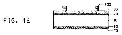
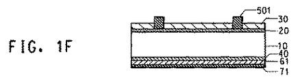
図1で示される参照符号を以下に説明する。
10:p型シリコン基板
20:n型拡散層
30:窒化シリコン膜、酸化チタン膜、または酸化シリコン膜
40:p+層(裏面フィールド:BSF(back surface field))
60:裏面側に形成されたアルミニウムペースト
61:アルミニウム裏面電極(裏面アルミニウムペーストを焼成することにより得られる)
70:裏側に形成された銀または銀/アルミニウムペースト
71:銀または銀/アルミニウム裏面電極(裏面銀ペーストを焼成することにより得られる)
500:本発明による前面側に形成された銀ペースト
501:本発明による銀の前面電極(前面側銀ペーストを焼成することにより形成される)
Reference numerals shown in FIG. 1 will be described below.
10: p-type silicon substrate 20: n-type diffusion layer 30: silicon nitride film, titanium oxide film, or silicon oxide film 40: p + layer (back surface field: BSF (back surface field))
60: Aluminum paste formed on the back surface 61: Aluminum back electrode (obtained by baking the back surface aluminum paste)
70: Silver or silver / aluminum paste formed on the back side 71: Silver or silver / aluminum back electrode (obtained by firing the back silver paste)
500:
向上された効率を有する改善された太陽電池が必要である。増大された高さを有する狭い導体線の形成に好適な導電性組成物が必要である。本発明の一態様はサブミクロン粒子を含む組成物に関する。組成物は厚膜組成物であってよい。これらの組成物は太陽電池電極を形成するために使用することができる。電極は太陽電池の前面側にあってよい。一実施形態では、電極線は狭く、そして増大された高さを有することができる。 There is a need for improved solar cells with improved efficiency. There is a need for a conductive composition suitable for forming narrow conductor wires having increased height. One aspect of the present invention relates to a composition comprising submicron particles. The composition may be a thick film composition. These compositions can be used to form solar cell electrodes. The electrode may be on the front side of the solar cell. In one embodiment, the electrode lines can be narrow and have an increased height.
本明細書で使用されるように、「厚膜組成物」とは、基板上で焼成されると1〜100ミクロンの厚さを有する組成物を指す。厚膜組成物は導電性材料、ガラス組成物、有機ビヒクルを含んでよい。厚膜組成物は追加成分を含んでよい。本明細書で使用されるように、追加成分は「添加剤」と称される。 As used herein, “thick film composition” refers to a composition having a thickness of 1 to 100 microns when fired on a substrate. The thick film composition may include a conductive material, a glass composition, and an organic vehicle. The thick film composition may include additional components. As used herein, an additional component is referred to as an “additive”.
本明細書に記載の組成物は、1つまたは複数の電気的機能材料と、有機媒体中に分散した1つまたは複数のガラスフリットとを含む。これらの組成物は厚膜組成物であってよい。組成物はまた1つまたは複数の添加剤を含んでよい。例示的な添加剤としては、金属、金属酸化物、または焼成中にこれらの金属酸化物を生成することができる任意の化合物が挙げられる。 The compositions described herein include one or more electrically functional materials and one or more glass frits dispersed in an organic medium. These compositions may be thick film compositions. The composition may also include one or more additives. Exemplary additives include metals, metal oxides, or any compound that can produce these metal oxides during firing.
一実施形態では、電気的機能粉体は導電性粉体であってよい。一実施形態では、組成物(例えば導電性組成物)は、半導体装置において使用することができる。本実施形態の一態様では、半導体装置は太陽電池またはフォトダイオードであってよい。本実施形態の別の態様では、半導体装置は広範な半導体装置の1つであってよい。一実施形態では、半導体装置は太陽電池であってよい。 In one embodiment, the electrically functional powder may be a conductive powder. In one embodiment, a composition (eg, a conductive composition) can be used in a semiconductor device. In one aspect of this embodiment, the semiconductor device may be a solar cell or a photodiode. In another aspect of this embodiment, the semiconductor device may be one of a wide range of semiconductor devices. In one embodiment, the semiconductor device may be a solar cell.
一実施形態では、本明細書に記載の厚膜組成物は、太陽電池において使用することができる。本実施形態の一態様では、太陽電池効率は基準太陽電池セルの70%より高いかもしれない。別の実施形態では、太陽電池効率は基準太陽電池セルの80%より高いかもしれない。太陽電池効率は基準太陽電池セルの90%より高いかもしれない。 In one embodiment, the thick film compositions described herein can be used in solar cells. In one aspect of this embodiment, the solar cell efficiency may be higher than 70% of the reference solar cell. In another embodiment, the solar cell efficiency may be higher than 80% of the reference solar cell. Solar cell efficiency may be higher than 90% of the reference solar cell.
一実施形態では、分散液中の無機成分に対する厚膜組成物中の有機媒体の比率は、当業者により決定されるペーストの塗布方法と使用される有機媒体の種類に依存してよい。一実施形態では、分散液は、良好な濡れ性を得るために70〜95wt%の無機成分と5〜30wt%の有機媒体(ベヒクル)を含んでよい。 In one embodiment, the ratio of the organic medium in the thick film composition to the inorganic components in the dispersion may depend on the paste application method determined by those skilled in the art and the type of organic medium used. In one embodiment, the dispersion may include 70-95 wt% inorganic components and 5-30 wt% organic medium (vehicle) to obtain good wettability.
一実施形態では、無機成分の一部はサブミクロン粒子であってよい。本実施形態の一態様では、サブミクロン粒子は0.1〜1ミクロンの平均粒径d50を有することができる。別の態様では、サブミクロン粒子は0.1〜0.8ミクロンの平均粒径d50を有することができる。別の態様では、サブミクロン粒子は0.2〜0.6ミクロンの平均粒径d50を有することができる。 In one embodiment, some of the inorganic components may be submicron particles. In one aspect of this embodiment, the submicron particles can have an average particle size d50 of 0.1 to 1 micron. In another aspect, the submicron particles can have an average particle size d50 of 0.1 to 0.8 microns. In another aspect, the submicron particles can have an average particle size d50 of 0.2 to 0.6 microns.
一実施形態では、サブミクロン粒子は組成物の1〜15wt%であってよい。別の実施形態では、サブミクロン粒子は組成物の2〜10wt%であってよい。別の実施形態では、サブミクロン粒子は組成物の3〜6wt%であってよい。 In one embodiment, the submicron particles may be 1-15 wt% of the composition. In another embodiment, the submicron particles may be 2-10 wt% of the composition. In another embodiment, the submicron particles may be 3-6 wt% of the composition.
一実施形態では、サブミクロン粒子は導電性材料の一部を含んでよい。一態様では、導電性材料の1〜15wt%はサブミクロン粒子であってよい。別の態様では、導電性材料の2〜10wt%はサブミクロン粒子であってよい。別の態様では、導電性組成物の3〜6wt%はサブミクロン粒子であってよい。 In one embodiment, the submicron particles may include a portion of a conductive material. In one aspect, 1-15 wt% of the conductive material may be submicron particles. In another aspect, 2-10 wt% of the conductive material may be submicron particles. In another aspect, 3-6 wt% of the conductive composition may be submicron particles.
一実施形態では、組成物の一部は1.5〜10ミクロンの平均粒径d50を有することができる。本実施形態の一態様では、組成物の無機成分の85〜99wt%は1.5〜10ミクロンの平均粒径d50を有することができる。本実施形態の一態様では、組成物の一部は2.0〜7.0ミクロンの平均粒径d50を有することができる。本実施形態の一態様では、組成物の一部は2.5〜5.0ミクロンの平均粒径d50を有することができる。 In one embodiment, a portion of the composition can have an average particle size d50 of 1.5 to 10 microns. In one aspect of this embodiment, 85 to 99 wt% of the inorganic components of the composition can have an average particle size d50 of 1.5 to 10 microns. In one aspect of this embodiment, a portion of the composition can have an average particle size d50 of 2.0 to 7.0 microns. In one aspect of this embodiment, a portion of the composition can have an average particle size d50 of 2.5 to 5.0 microns.
別の態様では、導電性材料は銀を含んでよい。一態様では、導電性材料の50〜100wt%は銀であってよい。別の態様では、導電性材料の70〜99wt%、70〜98wt%または80〜95wt%は銀であってよい。 In another aspect, the conductive material may include silver. In one aspect, 50-100 wt% of the conductive material may be silver. In another aspect, 70-99 wt%, 70-98 wt%, or 80-95 wt% of the conductive material may be silver.
ガラスフリット
本発明の一態様では、組成物はガラスフリット組成物を含む。本発明に有用なガラスフリット組成物は当業者により容易に理解される。例えば、前面側の太陽電池電極を作製するために使用される組成物に有用なガラスフリット組成物を使用してよい。例示的なガラスフリット組成物は硼珪酸鉛ガラスを含む。一実施形態では、本発明に有用なガラスフリット組成物は20〜24wt%のSiO2、0.2〜0.8wt%のAl2O3、40〜60wt%のPbO、5〜8wt%のB2O3を含んでよい。一実施形態では、ガラスフリット組成物はまた随意的に3〜7wt%のTiO2を含んでよい。一実施形態では、ガラスフリット組成物はまた随意的に1つまたは複数のフッ素含有成分(限定しないがフッ素、フッ化物、酸化フッ化金属化合物等の塩類を含む)を含んでよい。このようなフッ素含有成分としては、限定しないがPbF2、BiF3、AlF3、NaF、LiF、KF、CsF、ZrF4、TiF4、および/またはZnF2が挙げられる。一実施形態では、ガラスフリット組成物は8〜13wt%のPbF2を含んでよい。
Glass frit In one aspect of the invention, the composition comprises a glass frit composition. Glass frit compositions useful in the present invention are readily understood by those skilled in the art. For example, a glass frit composition useful for the composition used to make the front side solar cell electrode may be used. An exemplary glass frit composition includes lead borosilicate glass. In one embodiment, useful glass frit compositions of the present invention is SiO 2 of 20~24wt%, 0.2~0.8wt% of Al 2 O 3, 40~60wt% of PbO, 5-8 wt-% of B 2 O 3 may be included. In one embodiment, the glass frit composition may also optionally include 3-7 wt% TiO 2 . In one embodiment, the glass frit composition may also optionally include one or more fluorine-containing components, including but not limited to salts such as fluorine, fluorides, metal oxyfluoride compounds, and the like. Such fluorine-containing component, but not limited to PbF 2, BiF 3, AlF 3 , NaF, LiF, KF, CsF, ZrF 4, TiF 4, and / or ZnF 2 and the like. In one embodiment, the glass frit composition may include PbF 2 of 8-13 weight%.
本実施形態の別の態様では、厚膜組成物は、有機媒体中に分散した電気的機能粉体とガラスセラミックフリットを含んでよい。一実施形態では、これらの厚膜導体組成物は半導体装置において使用することができる。本実施形態の一態様では、半導体装置は太陽電池またはフォトダイオードであってよい。 In another aspect of this embodiment, the thick film composition may include electrically functional powder and glass ceramic frit dispersed in an organic medium. In one embodiment, these thick film conductor compositions can be used in semiconductor devices. In one aspect of this embodiment, the semiconductor device may be a solar cell or a photodiode.
導電性材料
一実施形態では、厚膜組成物は、適切な電気的機能特性を組成物に与える機能相を含んでよい。一実施形態では、電気的機能粉体は導電性粉体であってよい。一実施形態では、電気的機能相は導電性材料(本明細書では導電性粒子とも称する)を含んでよい。導電性粒子は例えば導電性粉体、導電性フレークまたはその混合物を含んでよい。
Conductive Material In one embodiment, the thick film composition may include a functional phase that imparts appropriate electrical functional properties to the composition. In one embodiment, the electrically functional powder may be a conductive powder. In one embodiment, the electrical functional phase may include a conductive material (also referred to herein as conductive particles). The conductive particles may include, for example, conductive powder, conductive flakes, or a mixture thereof.
一実施形態では、導電性粒子はAgを含んでよい。別の実施形態では、導電性粒子は銀(Ag)とアルミニウム(Al)を含んでよい。別の実施形態では、導電性粒子は例えばCu、Au、Ag、Pd、Pt、Al、Ag−Pd、Pt−Au等の1つまたは複数を含んでよい。一実施形態では、導電性粒子は、(1)Al、Cu、Au、Ag、Pd、Pt、(2)Al、Cu、Au、Ag、Pd、Ptの合金、(3)これらの混合物の1つまたは複数を含んでよい。 In one embodiment, the conductive particles may include Ag. In another embodiment, the conductive particles may include silver (Ag) and aluminum (Al). In another embodiment, the conductive particles may include one or more of, for example, Cu, Au, Ag, Pd, Pt, Al, Ag—Pd, Pt—Au, and the like. In one embodiment, the conductive particles comprise (1) Al, Cu, Au, Ag, Pd, Pt, (2) an alloy of Al, Cu, Au, Ag, Pd, Pt, (3) 1 of these mixtures. One or more may be included.
一実施形態では、組成物の機能相は、導電性である被覆または非被覆銀粒子を含んでよい。銀粒子が被覆される実施形態では、銀粒子は界面活性剤で少なくとも部分的に覆われる。一実施形態では、界面活性剤は以下の非限定的界面活性剤の1つまたは複数を含んでよい:ステアリン酸、パルミチン酸、ステアリン酸の塩、パルミチン酸塩、ラウリン酸、パルミチン酸、オレイン酸、ステアリン酸、カプリン酸、ミリスチン酸およびリノール酸の塩、そしてこれらの混合物。対イオンは限定しないが水素、アンモニウム、ナトリウム、カリウムおよびこれらの混合物であってよい。 In one embodiment, the functional phase of the composition may include coated or uncoated silver particles that are electrically conductive. In embodiments where silver particles are coated, the silver particles are at least partially covered with a surfactant. In one embodiment, the surfactant may comprise one or more of the following non-limiting surfactants: stearic acid, palmitic acid, stearic acid salt, palmitic acid salt, lauric acid, palmitic acid, oleic acid , Salts of stearic acid, capric acid, myristic acid and linoleic acid, and mixtures thereof. The counter ion can be, but is not limited to, hydrogen, ammonium, sodium, potassium, and mixtures thereof.
一実施形態では、銀はペースト組成物の60〜90wt%であってよい。別の実施形態では、銀はペースト組成物の70〜85wt%であってよい。別の実施形態では、銀はペースト組成物の75〜85wt%であってよい。別の実施形態では、銀はペースト組成物の78〜82wt%であってよい。 In one embodiment, the silver may be 60-90 wt% of the paste composition. In another embodiment, the silver may be 70-85 wt% of the paste composition. In another embodiment, the silver may be 75-85 wt% of the paste composition. In another embodiment, the silver may be 78-82 wt% of the paste composition.
一実施形態では、銀は組成物中の固体の90〜99wt%であってよい(すなわち有機ビヒクルを除いた)。別の実施形態では、銀は組成物中の固体の92〜97wt%であってよい。別の実施形態では、銀は組成物中の固体の93〜95wt%であってよい。 In one embodiment, the silver may be 90-99 wt% of the solids in the composition (i.e. excluding the organic vehicle). In another embodiment, the silver may be 92-97 wt% of the solids in the composition. In another embodiment, the silver may be 93-95 wt% of the solids in the composition.
本明細書で使用されるように、「粒径」は「平均粒径」を意味するものとし、「平均粒径」は50%体積分布粒径を意味する。体積分布粒径は、限定しないがMicrotrac粒径分析器を使用するレーザー回折および分散法を含む当業者により理解される多くの方法により決定されてよい。 As used herein, “particle size” shall mean “average particle size” and “average particle size” means 50% volume distribution particle size. The volume distribution particle size may be determined by a number of methods understood by those skilled in the art including, but not limited to, laser diffraction and dispersion methods using a Microtrac particle size analyzer.
一実施形態では、導電性材料の一部はサブミクロン粒子であってよい。本実施形態の一態様では、サブミクロン粒子は0.1〜1ミクロンの平均粒径d50を有することができる。別の態様では、サブミクロン粒子は0.1〜0.8ミクロンの平均粒径d50を有することができる。別の態様では、サブミクロン粒子は0.2〜0.6ミクロンの平均粒径d50を有することができる。 In one embodiment, the portion of the conductive material may be submicron particles. In one aspect of this embodiment, the submicron particles can have an average particle size d50 of 0.1 to 1 micron. In another aspect, the submicron particles can have an average particle size d50 of 0.1 to 0.8 microns. In another aspect, the submicron particles can have an average particle size d50 of 0.2 to 0.6 microns.
一実施形態では、導電性材料の1〜15wt%はサブミクロン粒子であってよい。別の態様では、導電性材料の2〜10wt%はサブミクロン粒子であってよい。別の態様では、導電性組成物の3〜6wt%はサブミクロン粒子であってよい。 In one embodiment, 1-15 wt% of the conductive material may be submicron particles. In another aspect, 2-10 wt% of the conductive material may be submicron particles. In another aspect, 3-6 wt% of the conductive composition may be submicron particles.
一実施形態では、導電性材料の一部は1.5〜10ミクロンの平均粒径d50を有することができる。本実施形態の一態様では、導電性材料の85〜99wt%は1.5〜10ミクロンの平均粒径d50を有することができる。本実施形態の一態様では、導電性材料の一部は2.0〜7.0ミクロンの平均粒径d50を有することができる。本実施形態の一態様では、導電性材料の一部は2.5〜5.0ミクロンの平均粒径d50を有することができる。 In one embodiment, a portion of the conductive material can have an average particle size d50 of 1.5 to 10 microns. In one aspect of this embodiment, 85-99 wt% of the conductive material can have an average particle size d50 of 1.5-10 microns. In one aspect of this embodiment, a portion of the conductive material can have an average particle size d50 of 2.0 to 7.0 microns. In one aspect of this embodiment, a portion of the conductive material can have an average particle size d50 of 2.5 to 5.0 microns.
添加剤
一実施形態では、厚膜組成物は1つまたは複数の添加剤を含んでよい。一実施形態では、添加剤は以下の1つまたは複数から選択されてよい:(a)Zn、Pb、Bi、Gd、Ce、Zr、Ti、Mn、Sn、Ru、Co、Fe、Cu、Crから選択される金属、(b)Zn、Pb、Bi、Gd、Ce、Zr、Ti、Mn、Sn、Ru、Co、Fe、Cu、Crから選択される1つまたは複数の金属の金属酸化物、(c)焼成されると(b)の金属酸化物を生成可能な任意の化合物、(d)それらの混合物。
Additives In one embodiment, the thick film composition may include one or more additives. In one embodiment, the additive may be selected from one or more of the following: (a) Zn, Pb, Bi, Gd, Ce, Zr, Ti, Mn, Sn, Ru, Co, Fe, Cu, Cr (B) a metal oxide of one or more metals selected from Zn, Pb, Bi, Gd, Ce, Zr, Ti, Mn, Sn, Ru, Co, Fe, Cu, Cr (C) any compound capable of producing the metal oxide of (b) upon firing, (d) a mixture thereof.
一実施形態では、添加剤はZn含有添加剤を含んでよい。Zn含有添加剤は、(a)Zn、(b)Znの金属酸化物、(c)焼成されるとZnの金属酸化物を生成可能な任意の化合物、(d)その混合物の1つまたは複数を含んでよい。一実施形態では、Zn含有添加剤はZn樹脂酸塩を含んでよい。 In one embodiment, the additive may include a Zn-containing additive. Zn-containing additive is: (a) Zn, (b) Zn metal oxide, (c) any compound capable of producing Zn metal oxide upon firing, (d) one or more of the mixtures May be included. In one embodiment, the Zn-containing additive may comprise a Zn resinate.
一実施形態では、Zn含有添加剤はZnOを含んでよい。一実施形態では、ZnOの一部はサブミクロン粒子を含んでよい。 In one embodiment, the Zn-containing additive may include ZnO. In one embodiment, the portion of ZnO may include submicron particles.
一実施形態では、ZnOは全組成の2−10wt%の範囲の組成物中に存在してよい。一実施形態では、ZnOは全組成の3−7wt%の範囲の組成物中に存在してよい。一実施形態では、ZnOは全組成の4−6wt%の範囲の組成物中に存在してよい。 In one embodiment, ZnO may be present in the composition in the range of 2-10 wt% of the total composition. In one embodiment, ZnO may be present in the composition in the range of 3-7 wt% of the total composition. In one embodiment, ZnO may be present in the composition in the range of 4-6 wt% of the total composition.
有機媒体
一実施形態では、本明細書に記載の厚膜組成物は有機媒体を含んでよい。無機成分は、例えばペーストを形成するための機械的な混合により有機媒体と混合されてよい。様々な不活性粘性物質を有機媒体として使用することができる。一実施形態では、有機媒体は無機成分が適切な安定度で分散されたものであってよい。一実施形態では、媒体の流動特性は、組成物に対し、固体の安定分散性、スクリーン印刷のための適切な粘度とチキソトロピー、基板およびペースト固体の適切な濡れ性、良好な乾燥速度、および良好な焼成特性を含むある塗布性を貸与することができる。一実施形態では、厚膜組成物中に使用される有機ビヒクルは非水性不活性液であってよい。増粘剤、安定剤、および/または他の一般の添加剤を含んでも含まなくてよい様々な有機ビヒクルの使用が考えられる。有機媒体は重合体の溶媒溶液であってよい。一実施形態では、有機媒体はまた界面活性剤など1つまたは複数の成分を含んでよい。一実施形態では、重合体はエチルセルロースであってよい。他の例示的な重合体としては、エチルヒドロキシエチルセルロース、ウッドロジン、エチルセルロースとフェノール樹脂の混合物、低級アルコールのポリメタクリレート、エチレングリコールモノアセタートのモノブチルエーテル、またはこれらの混合物が挙げられる。一実施形態では、本明細書に記載の厚膜組成物に有用な溶媒としては、エステルアルコール、アルファまたはベータテルピネオールなどのテルペン、あるいはこれらとケロシン、フタル酸ジブチル、ブチルカルビトール、ブチルカルビトールアセタート、ヘキシレングリコール、高沸点アルコール、アルコールエステルなどの他の溶媒との混合物が挙げられる。別の実施形態では、有機媒体は、基板への塗布後に急速な硬化を促進するための揮発性液体を含んでよい。
Organic Medium In one embodiment, the thick film compositions described herein may include an organic medium. The inorganic component may be mixed with the organic medium, for example by mechanical mixing to form a paste. Various inert viscous materials can be used as the organic medium. In one embodiment, the organic medium may be one in which inorganic components are dispersed with appropriate stability. In one embodiment, the rheological properties of the media are, for the composition, stable solid dispersion, suitable viscosity and thixotropy for screen printing, adequate wettability of substrates and paste solids, good drying speed, and good. Some applicability including various firing characteristics can be lent. In one embodiment, the organic vehicle used in the thick film composition may be a non-aqueous inert liquid. The use of various organic vehicles that may or may not include thickeners, stabilizers, and / or other common additives is contemplated. The organic medium may be a polymer solvent solution. In one embodiment, the organic medium may also include one or more components such as a surfactant. In one embodiment, the polymer may be ethyl cellulose. Other exemplary polymers include ethyl hydroxyethyl cellulose, wood rosin, a mixture of ethyl cellulose and phenolic resin, lower alcohol polymethacrylate, ethylene glycol monoacetate monobutyl ether, or mixtures thereof. In one embodiment, solvents useful for the thick film compositions described herein include ester alcohols, terpenes such as alpha or beta terpineol, or kerosene, dibutyl phthalate, butyl carbitol, butyl carbitol acetate. Examples thereof include mixtures with other solvents such as tart, hexylene glycol, high-boiling alcohols and alcohol esters. In another embodiment, the organic medium may include a volatile liquid to promote rapid curing after application to the substrate.
一実施形態では、例えば、重合体は全組成の8wt%から11wt%の範囲の有機媒体中に存在してよい。厚膜銀の組成は、有機媒体との所定のスクリーン印刷可能粘度に調節されてよい。 In one embodiment, for example, the polymer may be present in an organic medium ranging from 8 wt% to 11 wt% of the total composition. The composition of the thick film silver may be adjusted to a predetermined screen printable viscosity with the organic medium.
焼成厚膜組成物
一実施形態では、有機媒体は半導体装置の乾燥および焼成中に除去されてよい。一態様では、ガラスフリット、Ag、添加剤は、電極を形成するために焼成中に焼結させられてよい。焼成された電極は、焼成および焼結処理から生じる成分、組成物等を含んでよい。
Firing Thick Film Composition In one embodiment, the organic medium may be removed during drying and firing of the semiconductor device. In one aspect, the glass frit, Ag, and additive may be sintered during firing to form an electrode. The fired electrode may include components, compositions, etc. resulting from the firing and sintering processes.
本実施形態の一態様では、半導体装置は太陽電池またはフォトダイオードであってよい。 In one aspect of this embodiment, the semiconductor device may be a solar cell or a photodiode.
半導体装置の製造方法
一実施形態は半導体装置を製造する方法に関する。一実施形態では、半導体装置は太陽電池装置に使用することができる。半導体装置は、焼成前に本明細書に記載の組成物を含んでよい前面側電極(照射側)を含むことができる。
FIELD Embodiments described herein relate generally to a method for manufacturing a semiconductor device. In one embodiment, the semiconductor device can be used for a solar cell device. The semiconductor device can include a front side electrode (irradiation side) that may include the composition described herein prior to firing.
一実施形態では、半導体装置の製造方法は、(a)半導体基板を設ける工程、(b)半導体基板に絶縁膜を塗布する工程、(c)絶縁膜に本明細書に記載の組成物を塗布する工程、(d)装置を焼成する工程を含む。 In one embodiment, a method for manufacturing a semiconductor device includes (a) a step of providing a semiconductor substrate, (b) a step of applying an insulating film to the semiconductor substrate, and (c) applying the composition described herein to the insulating film. And (d) a step of firing the apparatus.
本明細書に記載の方法と装置に有用な例示的な半導体基板は当業者により理解される。例示的な半導体基板としては、限定しないが単結晶シリコン、多結晶シリコン、リボンシリコンが挙げられる。半導体基板は接合を有することができる。半導体基板をリンとホウ素でドープしてp/n接合を形成してよい。半導体基板のドープ方法は当業者により理解される。 Exemplary semiconductor substrates useful in the methods and apparatus described herein will be understood by those skilled in the art. Exemplary semiconductor substrates include, but are not limited to single crystal silicon, polycrystalline silicon, and ribbon silicon. The semiconductor substrate can have a bond. The semiconductor substrate may be doped with phosphorus and boron to form a p / n junction. Those skilled in the art understand how to dope semiconductor substrates.
当業者により理解されるように、半導体基板は寸法(長さ×幅)と厚さが変化してよい。非限定的な実施例では、半導体基板の厚さは50〜500ミクロン、100〜300ミクロン、または140〜200ミクロンであってよい。非限定的な実施例では、半導体基板の長さと幅は両者とも等しく100〜250mm、125〜200mm、または125〜156mmであってよい。 As will be appreciated by those skilled in the art, the semiconductor substrate may vary in size (length x width) and thickness. In non-limiting examples, the thickness of the semiconductor substrate can be 50-500 microns, 100-300 microns, or 140-200 microns. In non-limiting examples, the length and width of the semiconductor substrate may both be 100-250 mm, 125-200 mm, or 125-156 mm.
本明細書に記載の方法と装置に有用な例示的な絶縁膜は当業者により理解される。例示的な絶縁膜としては限定しないが、窒化シリコン、酸化シリコン、酸化チタン、SiNx:H、水素化アモルファス窒化シリコン、酸化シリコン/酸化チタン膜が挙げられる。絶縁膜は、PECVD、CVD、および/または当業者によく知られた他の技術により形成されてよい。絶縁膜が窒化シリコンである一実施形態では、窒化シリコン膜はプラズマ化学気相成長法(PECVD)、熱CVD処理、または物理気相蒸着法(PVD)で形成されてよい。絶縁膜が酸化シリコンである実施形態では、酸化シリコン膜は、熱酸化、熱CVD、プラズマCVD、またはPVDにより形成されてよい。絶縁膜(または層)は反射防止被膜(ARC:anti−reflective coating)と称すことがある。 Exemplary insulating films useful in the methods and apparatus described herein will be understood by those skilled in the art. Exemplary insulating films include, but are not limited to, silicon nitride, silicon oxide, titanium oxide, SiN x : H, hydrogenated amorphous silicon nitride, and silicon oxide / titanium oxide films. The insulating film may be formed by PECVD, CVD, and / or other techniques well known to those skilled in the art. In one embodiment where the insulating film is silicon nitride, the silicon nitride film may be formed by plasma enhanced chemical vapor deposition (PECVD), thermal CVD processing, or physical vapor deposition (PVD). In embodiments where the insulating film is silicon oxide, the silicon oxide film may be formed by thermal oxidation, thermal CVD, plasma CVD, or PVD. The insulating film (or layer) may be referred to as an anti-reflective coating (ARC).
本明細書に記載の組成物は、限定しないがスクリーン印刷、インクジェット、共押出し、シリンジ分注、直接描画、噴霧インクジェットを含む当業者によく知られた様々な方法によりARC塗布半導体基板に塗布されてよい。一実施形態では、組成物は、参照により本明細書に援用する米国特許出願公開第2003/0100824号明細書に記載された方法と装置を使用して基板に塗布されてよい。組成物はパターンで塗布されてよい。組成物は所定形状でかつ所定位置において塗布されてよい。一実施形態では、組成物は前面側電極の導電性フィンガーとバスバーの両方を形成するために使用することができる。一実施形態では、導電性フィンガーの線幅は10〜200ミクロン、40〜150ミクロン、または60〜100ミクロンであってよい。一実施形態では、導電性フィンガーの線幅は10〜100ミクロン、15〜80ミクロン、または20〜75ミクロンであってよい。一実施形態では、導電性フィンガーの線の厚さは5〜50ミクロン、10〜35ミクロン、または15〜30ミクロンであってよい。別の実施形態では、組成物は、導電性Si接触フィンガーを形成するために使用することができる。 The compositions described herein can be applied to ARC coated semiconductor substrates by a variety of methods well known to those skilled in the art including, but not limited to, screen printing, inkjet, coextrusion, syringe dispensing, direct drawing, spray inkjet. It's okay. In one embodiment, the composition may be applied to a substrate using the methods and apparatus described in US Patent Publication No. 2003/0100824, which is incorporated herein by reference. The composition may be applied in a pattern. The composition may be applied in a predetermined shape and at a predetermined location. In one embodiment, the composition can be used to form both conductive fingers and bus bars of the front electrode. In one embodiment, the line width of the conductive fingers may be 10-200 microns, 40-150 microns, or 60-100 microns. In one embodiment, the line width of the conductive fingers may be 10-100 microns, 15-80 microns, or 20-75 microns. In one embodiment, the conductive finger line thickness may be 5-50 microns, 10-35 microns, or 15-30 microns. In another embodiment, the composition can be used to form conductive Si contact fingers.
ARC塗布半導体基板に被覆された組成物は、当業者により理解されるように、例えば0.5〜10分間乾燥されその後焼成されてよい。一実施形態では、揮発性溶剤および有機物は乾燥処理中に除去されてよい。焼成条件は当業者により理解されるだろう。例示的かつ非限定的焼成条件で、シリコンウェーハ基板は、1秒〜2分間600〜900°Cの最高温度まで加熱される。一実施形態では、焼成中に到達するシリコンウェーハ最高温度は1〜10秒間で650〜800°Cの範囲である。別の実施形態では、導電性厚膜組成物から形成される電極は、酸素と窒素の混合ガスからなる雰囲気中で焼成されてよい。この焼成処理は有機媒体を除去し、ガラスフリットを導電性厚膜組成物中のAg粉体で焼結させる。別の実施形態では、導電性厚膜組成物から形成される電極は、酸素を含まない不活性雰囲気中で有機媒体除去温度より高い温度で焼成されてよい。この焼成処理は、厚膜組成物中の銅などの卑金属導電性材料を焼結または溶融する。 The composition coated on the ARC coated semiconductor substrate may be dried and then fired, for example, for 0.5-10 minutes, as will be appreciated by those skilled in the art. In one embodiment, volatile solvents and organics may be removed during the drying process. Firing conditions will be understood by those skilled in the art. Under exemplary and non-limiting firing conditions, the silicon wafer substrate is heated to a maximum temperature of 600-900 ° C. for 1 second to 2 minutes. In one embodiment, the maximum silicon wafer temperature reached during firing is in the range of 650-800 ° C. for 1-10 seconds. In another embodiment, the electrode formed from the conductive thick film composition may be fired in an atmosphere composed of a mixed gas of oxygen and nitrogen. This firing process removes the organic medium and sinters the glass frit with the Ag powder in the conductive thick film composition. In another embodiment, the electrode formed from the conductive thick film composition may be fired at a temperature above the organic media removal temperature in an oxygen free inert atmosphere. This firing process sinters or melts a base metal conductive material such as copper in the thick film composition.
一実施形態では、焼成中、焼成される電極(好ましくはフィンガー)は絶縁膜と反応して絶縁膜に侵入し、シリコン基板との電気的接点を形成する。 In one embodiment, during firing, the fired electrode (preferably a finger) reacts with the insulating film to penetrate the insulating film and form an electrical contact with the silicon substrate.
別の実施形態では、焼成の前に、他の導電性および装置強化材料が半導体装置の反対型領域に塗布され、本明細書に記載の組成物と同時焼成または連続焼成される。装置の反対型領域は装置の反対側にある。上記材料は電気接点、パッシベーション層、はんだ付け可能なタブ領域として機能する。 In another embodiment, prior to firing, other conductive and device reinforcing materials are applied to the opposite areas of the semiconductor device and co-fired or continuously fired with the compositions described herein. The opposite area of the device is on the opposite side of the device. The material functions as an electrical contact, a passivation layer, and a solderable tab region.
一実施形態では、反対型領域は装置の非照射(裏)側にあってよい。本実施形態の一態様では、裏面導電性材料はアルミニウムを含んでよい。例示的な裏面アルミニウム含有組成物と塗布方法は、例えば参照により本明細書に援用する米国特許出願公開第2006/0272700号明細書に記載されている。 In one embodiment, the opposite area may be on the non-irradiated (back) side of the device. In one aspect of this embodiment, the backside conductive material may include aluminum. Exemplary backside aluminum-containing compositions and coating methods are described, for example, in US 2006/0272700, which is incorporated herein by reference.
別の態様では、はんだ付け可能なタブ材料はアルミニウムと銀とを含んでよい。アルミニウムと銀とを含む例示的なタブ組成物は、例えば参照により本明細書に援用する米国特許出願公開第2006/0231803号明細書に記載されている。 In another aspect, the solderable tab material may include aluminum and silver. Exemplary tab compositions comprising aluminum and silver are described, for example, in US Patent Application Publication No. 2006/0231803, which is incorporated herein by reference.
別の実施形態では、装置の反対型領域に塗布される材料は、並んで形成されているpおよびn領域のため、本明細書に記載の材料に隣接する。このような装置は、照射(前面)側の入射光を最大にするために装置の非照射(裏)側にすべての金属接触材料を配置する。 In another embodiment, the material applied to the opposite region of the device is adjacent to the materials described herein because of the p and n regions formed side by side. Such devices place all metal contact material on the non-irradiated (back) side of the device to maximize the incident light on the irradiated (front) side.
半導体装置は、接合を有する半導体基板とその主要面に形成された窒化シリコン絶縁膜とからなる構造部材から以下の方法により製造されてよい。半導体装置の製造方法は、絶縁膜に侵入する能力を有する導電性厚膜組成物を絶縁膜上に所定形状でかつ所定位置に塗布する(被覆および印刷するなどの)工程と、次に、導電性厚膜組成物が溶融して絶縁膜を貫通し、これによりシリコン基板との電気接点をもたらすように焼成する工程と、を含む。導電性厚膜組成物は、本明細書で説明したように有機ビヒクル内に分散される銀粉と、Zn含有添加剤と、300〜600°Cの軟化温度を有するガラスまたはガラス粉体混合物と、随意的には追加の金属/金属酸化物添加剤とからなる厚膜ペースト組成物である。 The semiconductor device may be manufactured by the following method from a structural member including a semiconductor substrate having a junction and a silicon nitride insulating film formed on the main surface thereof. A manufacturing method of a semiconductor device includes a step of applying a conductive thick film composition having an ability to penetrate an insulating film in a predetermined shape and at a predetermined position (such as coating and printing) on the insulating film, And firing the thick film composition to melt and penetrate the insulating film, thereby providing an electrical contact with the silicon substrate. The conductive thick film composition comprises a silver powder dispersed in an organic vehicle as described herein, a Zn-containing additive, a glass or glass powder mixture having a softening temperature of 300-600 ° C, Optionally, a thick film paste composition comprising an additional metal / metal oxide additive.
本発明の一実施形態は、本明細書に記載の方法で製造される半導体装置に関する。本明細書に記載の組成物を含む装置は上述のように珪酸亜鉛を含んでよい。 One embodiment of the invention relates to a semiconductor device manufactured by the method described herein. Devices comprising the compositions described herein may comprise zinc silicate as described above.
本発明の一実施形態は、上記方法で製造される半導体装置に関する。 One embodiment of the present invention relates to a semiconductor device manufactured by the above method.
本明細書に記載の厚膜組成物と共に利用可能なさらなる基板、装置、製造方法等は、その全体を参照により本明細書に援用する米国特許出願公開第2006/0231801号明細書、米国特許出願公開第2006/0231804号明細書、米国特許出願公開第2006/0231800号明細書に記載される。 Additional substrates, devices, manufacturing methods, etc. that can be used with the thick film compositions described herein are disclosed in US Patent Application Publication No. 2006/0231801, US Patent Application, which is hereby incorporated by reference in its entirety. This is described in Japanese Patent Application Publication No. 2006/0231804 and US Patent Application Publication No. 2006/0231800.
有機媒体は、約100℃の有機溶媒中に重合体を溶解することにより用意された。有機媒体中には、銀粉、ガラスフリット、酸化亜鉛、他の添加剤を含む他の成分が加えられた。生成された混合物は、厚膜ペースト製造業においてよく知られた3本ロール混練処理により分散された。表1に示す組成物I、II、IIIが形成された。 The organic medium was prepared by dissolving the polymer in an organic solvent at about 100 ° C. In the organic medium, other ingredients including silver powder, glass frit, zinc oxide and other additives were added. The resulting mixture was dispersed by a three roll kneading process well known in the thick film paste manufacturing industry. Compositions I, II and III shown in Table 1 were formed.
組成物IとIIのペーストは、印刷の前にRoki40L−SHP−200XSフィルタカプセルを通してろ過された。組成物IIIは濾過なしで使用された。 Composition I and II pastes were filtered through Roki 40L-SHP-200XS filter capsules prior to printing. Composition III was used without filtration.
ペーストは、ID/OD 50/75μmの再利用可能なセラミックペン先端を使用して、nScrypt Inc製3D−450 Smart Pump(商標)プリンターにより室温で評価された。ポンプ圧は10psi〜100psiであった。プリント速度は毎秒200mm〜毎秒300mmであった。ペン先端と基板表面間のギャップは150μmである。 The paste was evaluated at room temperature with a 3D-450 Smart Pump ™ printer from nScript Inc using a reusable ceramic pen tip with ID / OD 50/75 μm. The pump pressure was 10 psi to 100 psi. The printing speed was 200 mm / second to 300 mm / second. The gap between the pen tip and the substrate surface is 150 μm.
10本の4インチ長の線の群が印刷され、20分間150℃で箱型オーブン内で乾燥され、次に2分間850℃ピーク温度でベルト炉内で焼成された。 Groups of 10 4 inch long lines were printed, dried in a box oven at 150 ° C. for 20 minutes, and then fired in a belt furnace at 850 ° C. peak temperature for 2 minutes.

実施例I
組成物Iは、ペン先端が塞がれる前5分未満の間50psi未満のポンプ圧下で50/75ミクロンのペン先端を通過することができた。最良の結果の焼成された線は幅83ミクロン、高さ13ミクロンであった。
Example I
Composition I was able to pass through a 50/75 micron pen tip under a pump pressure of less than 50 psi for less than 5 minutes before the pen tip was plugged. The best results fired lines were 83 microns wide and 13 microns high.
実施例II
組成物Iは、ペン先端が塞がれる前30分未満の間60psi未満のポンプ圧下で75/125ミクロンのペン先端を通過することができた。最良の結果の焼成された線は幅100ミクロン、高さ12ミクロンであった。
Example II
Composition I was able to pass the 75/125 micron pen tip under a pump pressure of less than 60 psi for less than 30 minutes before the pen tip was plugged. The best results fired lines were 100 microns wide and 12 microns high.
実施例III
組成物IIは、印刷が停止される前少なくとも30分間10psi〜100psiの範囲のポンプ圧下で50/75ミクロンのペン先端を通過することができた。最良の結果の焼成された線は幅89ミクロン、高さ19ミクロンであった。
Example III
Composition II was able to pass through a 50/75 micron pen tip under pump pressure in the range of 10 psi to 100 psi for at least 30 minutes before printing was stopped. The best results fired lines were 89 microns wide and 19 microns high.
実施例IV
95.5対4.5の重量百分率比の組成物IIと組成物IIIの混合物は、印刷が停止される前少なくとも3時間10psi〜80psiの範囲のポンプ圧下で50/75ミクロンのペン先端を通過することができた。最良の結果の焼成された線は幅67ミクロン、高さ25ミクロンであった。
Example IV
Mixture of Composition II and Composition III in a 95.5 to 4.5 weight percentage ratio passes through a 50/75 micron pen tip under pump pressure in the range of 10 psi to 80 psi for at least 3 hours before printing is stopped. We were able to. The best results fired lines were 67 microns wide and 25 microns high.
実施例V
組成物IIIは、30psiより大きなポンプ圧下50/75ミクロンのペン先端を通して印刷することができなかった。30psi下では、印刷はペン先端が塞がれる前5秒未満の間続いた。
Example V
Composition III could not be printed through a 50/75 micron pen tip under a pump pressure greater than 30 psi. Under 30 psi, printing continued for less than 5 seconds before the pen tip was blocked.
実施例VI
組成物IIIは、60psiより大きなポンプ圧下75/125ミクロンのペン先端を通して印刷することができた。60psi下では、印刷はペン先端が塞がれる前5分未満の間続いた。
Example VI
Composition III could be printed through a 75/125 micron pen tip under a pump pressure greater than 60 psi. Under 60 psi, printing continued for less than 5 minutes before the pen tip was blocked.
実例VII
重量比率が90対10〜10対90の範囲の組成物IIとIIIの一連の混合物が用意され印刷された。組成物IIIの重量比率が30%より大きくなると、50/75ミクロンのペン先端は1分以内に塞がれた。
Example VII
A series of blends of Compositions II and III with weight ratios ranging from 90:10 to 10:90 were prepared and printed. When the weight ratio of Composition III was greater than 30%, the 50/75 micron pen tip was plugged within 1 minute.
実施例VIII
上記印刷された基板の効率を解析する。例示的な効率試験を以下に示す。実施例IVの太陽電池の効率が他の実施例の太陽電池の効率より大きくなることが予測される。
Example VIII
Analyze the efficiency of the printed substrate. An exemplary efficiency test is shown below. It is expected that the efficiency of the solar cell of Example IV will be greater than the efficiency of the solar cells of other examples.
試験手順−効率
本明細書に記載の方法に従って作製された太陽電池は変換効率について試験される。効率を試験する例示的な方法を以下に示す。
Test Procedure-Efficiency Solar cells made according to the methods described herein are tested for conversion efficiency. An exemplary method for testing efficiency is shown below.
一実施形態では、本明細書に記載の方法に従って作製された太陽電池は、市販の効率測定用のI−V試験装置(ST−1000)内に配置される。I−V試験装置内のXeアーク灯はよく知られた強度で直射日光を模擬し、電池の前面を照射した。 In one embodiment, solar cells made according to the methods described herein are placed in a commercially available IV test apparatus (ST-1000) for measuring efficiency. The Xe arc lamp in the IV test apparatus simulated the direct sunlight with a well-known intensity and irradiated the front surface of the battery.
試験装置は、電池のI−V特性曲線を確定するための約400の負荷抵抗設定で電流(I)と電圧(V)を測定するために多点直接接触法を使用する。充填率(FF)と効率(Eff)の両方はI−V特性曲線から計算される。 The test apparatus uses a multipoint direct contact method to measure current (I) and voltage (V) with a load resistance setting of about 400 to establish the battery's IV characteristic curve. Both filling factor (FF) and efficiency (Eff) are calculated from the IV characteristic curve.
Claims (15)
(b)前記半導体基板に前記絶縁膜を塗布する工程、
(c)前記半導体基板上の絶縁膜に前記厚膜組成物を塗布する工程、
(d)前記半導体、絶縁膜、及び厚膜組成物を焼成する工程、
を含む方法により製造される半導体装置であって、前記厚膜組成物は、
(i)1つまたは複数の導電性材料、
(ii)1つまたは複数の無機結合剤、
(iii)有機ビヒクル、
を含み、無機成分の1〜15%はサブミクロン粒子である、装置。 (A) preparing a semiconductor substrate, one or more insulating films, a thick film composition;
(B) applying the insulating film to the semiconductor substrate;
(C) applying the thick film composition to an insulating film on the semiconductor substrate;
(D) firing the semiconductor, insulating film, and thick film composition;
A thick film composition comprising: a semiconductor device manufactured by a method comprising:
(I) one or more conductive materials,
(Ii) one or more inorganic binders,
(Iii) an organic vehicle,
Wherein 1-15% of the inorganic components are submicron particles.
(a)1つまたは複数の導電性材料、
(b)1つまたは複数の無機結合剤、
(c)有機ビヒクル、
を含む組成物を含み、無機成分の1〜15%がサブミクロン粒子である、装置。 A semiconductor device including an electrode, wherein the electrode is
(A) one or more conductive materials,
(B) one or more inorganic binders,
(C) an organic vehicle,
A device comprising 1 to 15% of the inorganic component is submicron particles.
(a)Zn、Pb、Bi、Gd、Ce、Zr、Ti、Mn、Sn、Ru、Co、Fe、Cu、Crから選択される金属と、
(b)Zn、Pb、Bi、Gd、Ce、Zr、Ti、Mn、Sn、Ru、Co、Fe、Cu、Crから選択される1つまたは複数の金属の金属酸化物と、
(c)焼成されると(b)の金属酸化物を生成可能な任意の化合物と、
(d)それらの混合物と、
からなる群から選択される成分を含む、請求項9に記載の装置。 The one or more additives are:
(A) a metal selected from Zn, Pb, Bi, Gd, Ce, Zr, Ti, Mn, Sn, Ru, Co, Fe, Cu, Cr;
(B) a metal oxide of one or more metals selected from Zn, Pb, Bi, Gd, Ce, Zr, Ti, Mn, Sn, Ru, Co, Fe, Cu, Cr;
(C) any compound capable of producing the metal oxide of (b) upon firing;
(D) a mixture thereof;
The apparatus of claim 9, comprising a component selected from the group consisting of:
Applications Claiming Priority (3)
| Application Number | Priority Date | Filing Date | Title |
|---|---|---|---|
| US5660208P | 2008-05-28 | 2008-05-28 | |
| US61/056,602 | 2008-05-28 | ||
| PCT/US2009/045412 WO2009146356A1 (en) | 2008-05-28 | 2009-05-28 | Conductors for photovoltaic cells: compositions containing submicron particles |
Publications (2)
| Publication Number | Publication Date |
|---|---|
| JP2011522423A true JP2011522423A (en) | 2011-07-28 |
| JP2011522423A5 JP2011522423A5 (en) | 2012-07-12 |
Family
ID=40934860
Family Applications (1)
| Application Number | Title | Priority Date | Filing Date |
|---|---|---|---|
| JP2011511805A Withdrawn JP2011522423A (en) | 2008-05-28 | 2009-05-28 | Photovoltaic conductor: A composition containing submicron particles |
Country Status (6)
| Country | Link |
|---|---|
| EP (1) | EP2286417A1 (en) |
| JP (1) | JP2011522423A (en) |
| KR (1) | KR20110014676A (en) |
| CN (1) | CN102017013A (en) |
| TW (1) | TW201013699A (en) |
| WO (1) | WO2009146356A1 (en) |
Families Citing this family (1)
| Publication number | Priority date | Publication date | Assignee | Title |
|---|---|---|---|---|
| WO2012044281A1 (en) * | 2010-09-28 | 2012-04-05 | E. I. Du Pont De Nemours And Company | Conductive paste for solar cell electrode |
Family Cites Families (3)
| Publication number | Priority date | Publication date | Assignee | Title |
|---|---|---|---|---|
| JP3854103B2 (en) * | 2001-06-28 | 2006-12-06 | 住友ベークライト株式会社 | Conductive paste and semiconductor device using the paste |
| US7435361B2 (en) * | 2005-04-14 | 2008-10-14 | E.I. Du Pont De Nemours And Company | Conductive compositions and processes for use in the manufacture of semiconductor devices |
| US7556748B2 (en) * | 2005-04-14 | 2009-07-07 | E. I. Du Pont De Nemours And Company | Method of manufacture of semiconductor device and conductive compositions used therein |
-
2009
- 2009-05-28 JP JP2011511805A patent/JP2011522423A/en not_active Withdrawn
- 2009-05-28 WO PCT/US2009/045412 patent/WO2009146356A1/en active Application Filing
- 2009-05-28 CN CN2009801155914A patent/CN102017013A/en active Pending
- 2009-05-28 EP EP09755717A patent/EP2286417A1/en not_active Withdrawn
- 2009-05-28 KR KR1020107029441A patent/KR20110014676A/en not_active Application Discontinuation
- 2009-06-01 TW TW98118099A patent/TW201013699A/en unknown
Also Published As
| Publication number | Publication date |
|---|---|
| KR20110014676A (en) | 2011-02-11 |
| WO2009146356A1 (en) | 2009-12-03 |
| EP2286417A1 (en) | 2011-02-23 |
| CN102017013A (en) | 2011-04-13 |
| TW201013699A (en) | 2010-04-01 |
Similar Documents
| Publication | Publication Date | Title |
|---|---|---|
| JP5395995B2 (en) | Conductive compositions and methods used in the manufacture of semiconductor devices | |
| KR101086183B1 (en) | Thick film conductive composition and processes for use in the manufacture of semiconductor device | |
| JP5349738B2 (en) | Semiconductor device manufacturing method and conductive composition used therefor | |
| EP2720231B1 (en) | Electro-conductive pastes with salts with an anion consisting of halogen and oxygen in solar cell applications | |
| JP2011502330A (en) | Lead-free conductive composition and method of use in the manufacture of semiconductor devices: Mg-containing additives | |
| JP2011523492A (en) | Conductive composition and method of use in the manufacture of semiconductor devices | |
| US8748304B2 (en) | Devices containing silver compositions deposited by micro-deposition direct writing silver conductor lines | |
| JP2011503772A (en) | Conductive composition and method of use in manufacturing semiconductor devices: Mg-containing additive | |
| JP2006302891A (en) | Manufacturing method for semiconductor device and conductive composition used in it | |
| JP2011501866A (en) | Lead-free conductive composition and method of use in the manufacture of semiconductor devices: flux materials | |
| JP2011517117A (en) | Conductive composition and method of use in the manufacture of semiconductor devices | |
| JP2011519112A (en) | Conductive composition and method of use in the manufacture of semiconductor devices: flux materials | |
| JP2011502345A (en) | Conductive composition and method of use in the manufacture of semiconductor devices: multiple busbars | |
| KR20120066042A (en) | Thick-film conductive compositions with nano-sized zinc additive | |
| JP2012530664A (en) | Glass composition used in conductors for photovoltaic cells | |
| JP2011524068A (en) | Composition comprising submicron particles for use in photovoltaic cell conductors | |
| JP2011525700A (en) | Method of using compositions containing submicron particles used in photovoltaic cell conductors | |
| US8008179B2 (en) | Methods using silver compositions for micro-deposition direct writing silver conductor lines on photovoltaic wafers | |
| JP2013504177A (en) | Conductor for photovoltaic cells | |
| JP2011522423A (en) | Photovoltaic conductor: A composition containing submicron particles |
Legal Events
| Date | Code | Title | Description |
|---|---|---|---|
| A521 | Written amendment |
Free format text: JAPANESE INTERMEDIATE CODE: A523 Effective date: 20120523 |
|
| A621 | Written request for application examination |
Free format text: JAPANESE INTERMEDIATE CODE: A621 Effective date: 20120523 |
|
| A761 | Written withdrawal of application |
Free format text: JAPANESE INTERMEDIATE CODE: A761 Effective date: 20130313 |