JP2011517160A - High-speed digital converter - Google Patents
High-speed digital converter Download PDFInfo
- Publication number
- JP2011517160A JP2011517160A JP2010549822A JP2010549822A JP2011517160A JP 2011517160 A JP2011517160 A JP 2011517160A JP 2010549822 A JP2010549822 A JP 2010549822A JP 2010549822 A JP2010549822 A JP 2010549822A JP 2011517160 A JP2011517160 A JP 2011517160A
- Authority
- JP
- Japan
- Prior art keywords
- signal
- delay
- delayed
- tdc
- flip
- Prior art date
- Legal status (The legal status is an assumption and is not a legal conclusion. Google has not performed a legal analysis and makes no representation as to the accuracy of the status listed.)
- Pending
Links
Images

Classifications
-
- G—PHYSICS
- G04—HOROLOGY
- G04F—TIME-INTERVAL MEASURING
- G04F10/00—Apparatus for measuring unknown time intervals by electric means
- G04F10/005—Time-to-digital converters [TDC]
Landscapes
- Physics & Mathematics (AREA)
- General Physics & Mathematics (AREA)
- Analogue/Digital Conversion (AREA)
- Manipulation Of Pulses (AREA)
- Pulse Circuits (AREA)
Abstract
【解決手段】 時間ディジタル・コンバータ(TDC)がサブ・インバータ遅延分解能でサンプリングすることを可能にするための手法が開示されている。一実施形態では、TDC中の差動型D−Qフリップフロップへの入力は、シングルエンド型信号、およびこの信号の遅延された形態および反転された形態に接続されてこの信号の時間補間を可能にする。さらに、TDC中の第1遅延ラインおよび相補な遅延ラインの負荷の平衡を保つための手法が開示されている。
【選択図】 図3A technique is disclosed for enabling a time digital converter (TDC) to sample with sub-inverter delay resolution. In one embodiment, the input to the differential DQ flip-flop in the TDC is connected to a single-ended signal and the delayed and inverted forms of this signal to allow time interpolation of this signal To. Further, a technique for balancing the load of the first delay line and the complementary delay line in the TDC is disclosed.
[Selection] Figure 3
Description
本開示は時間ディジタル(time-to-digital)・コンバータ(TDC)のデザインに関し、より具体的には、サブ単位(unit、ユニット)の遅延分解能を有するTDCのデザインに関する。 The present disclosure relates to time-to-digital converter (TDC) designs, and more specifically to TDC designs with sub-unit delay resolution.
時間ディジタル・コンバータは、2つの出来事の間の経過時間間隔をディジタル表現したものを生成するように設計されている。TDCは時間間隔を離散化する。ちょうどAD変換器(ADC)がアナログ信号振幅を離散化するのと同様である。実際の時間間隔とこの時間間隔の離散化された形態(version)との間の差は、量子化誤差として知られており、TDCの分解能によって決定される。 Time digital converters are designed to produce a digital representation of the elapsed time interval between two events. TDC discretizes time intervals. Just like an analog-to-digital converter (ADC) discretizes the analog signal amplitude. The difference between the actual time interval and the discretized version of this time interval is known as the quantization error and is determined by the resolution of the TDC.
TDC分解能は、典型的にTDCの遅延線路の単位セル(ユニット・セル、unit cell)の遅延によって制限されている。例えば、遅延はインバータのゲート遅延であり得、これは使用された具体的な半導体処理技術の特徴である。ある高速TDC適用形態については、TDC分解能を単位セルの遅延を越えるまでに改善するための設計技術を有することが望ましいだろう。 The TDC resolution is typically limited by the unit cell delay of the TDC delay line. For example, the delay can be the gate delay of the inverter, which is a feature of the specific semiconductor processing technology used. For some high speed TDC applications, it may be desirable to have a design technique to improve the TDC resolution beyond the unit cell delay.
本開示の一側面は、信号Aの少なくとも1つの遅延された形態A(m)を生成するための遅延ラインであって、A(m)はAに対してm遅延単位(unit)だけ遅延されている、遅延ラインと、A(m)と信号B[A(m)]との間の時刻の差分をサンプリングするためのサンプリング機構であって、B[A(m)]はAに対して少なくとも1遅延単位だけ遅延されている、サンプリング機構と、を具備する時間ディジタル・コンバータ(TDC)を提供する。 One aspect of the present disclosure is a delay line for generating at least one delayed form A (m) of signal A, where A (m) is delayed with respect to A by m delay units. A sampling mechanism for sampling a delay line and a time difference between A (m) and signal B [A (m)], wherein B [A (m)] A time digital converter (TDC) comprising a sampling mechanism that is delayed by at least one delay unit.
本開示の別の側面は、信号Aの少なくとも1つの遅延された形態A(m)を生成することであって、A(m)はAに対してm遅延単位(unit)だけ遅延されている、生成することと、A(m)と信号B[A(m)]との間の時刻の差分をサンプリングすることであって、B[A(m)]はAに対して少なくとも1遅延単位だけ遅延されている、サンプリングすることと、を具備する、時間間隔をディジタル表現に変換するための方法を提供する。 Another aspect of the present disclosure is to generate at least one delayed form A (m) of signal A, where A (m) is delayed by m delay units with respect to A. Generating and sampling a time difference between A (m) and signal B [A (m)], where B [A (m)] is at least one delay unit relative to A A method is provided for converting a time interval into a digital representation comprising:
本開示のさらに別の側面は、信号Aの少なくとも1つの遅延された形態A(m)を生成するための手段であって、A(m)はAに対してm遅延単位(unit)だけ遅延されている、生成するための手段と、A(m)と信号B[A(m)]との間の時刻の差分をサンプリングするための手段であって、B[A(m)]はAに対して少なくとも1遅延単位だけ遅延されている、サンプリングするための手段と、を具備する、時間ディジタル・コンバータ(TDC)を提供する。 Yet another aspect of the present disclosure is a means for generating at least one delayed form A (m) of signal A, where A (m) is delayed by m delay units relative to A. Means for generating and means for sampling the time difference between A (m) and the signal B [A (m)], where B [A (m)] is A A time digital converter (TDC) comprising: means for sampling, delayed by at least one delay unit.
本開示のさらに別の側面は、コンピュータに、信号Aの少なくとも1つの遅延された形態A(m)を生成させるためのコードであって、A(m)はAに対してm遅延単位(unit)だけ遅延されている、生成させるためのコードと、コンピュータに、A(m)と信号B[A(m)]との間の時刻の差分をサンプリングさせるためのコードであって、B[A(m)]はAに対して少なくとも1遅延単位だけ遅延されている、サンプリングさせるためのコードと、を具備するコンピュータ可読媒体を具備する、時間間隔をディジタル表現に変換するためのコンピュータ・プログラム製品を提供する。 Yet another aspect of the disclosure is code for causing a computer to generate at least one delayed form A (m) of a signal A, where A (m) is m delay units relative to A. ) And a code for causing the computer to sample the time difference between A (m) and the signal B [A (m)], (M)] is a computer program product for converting a time interval into a digital representation comprising a computer readable medium comprising a code for sampling, delayed by at least one delay unit with respect to A I will provide a.
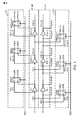
図1は、先行技術TDCの一部の実現形態を図示している。図1では、各々遅延TDを有する反転バッファB.nは、遅延ライン100を形成する。遅延ライン100は、元のシングルエンド型信号Aの漸次遅延された形態A(n)を生成する。ここで、nは遅延ライン100の0(遅延無し)から最大遅延までの間のインデックスである。
FIG. 1 illustrates some implementations of the prior art TDC. In Figure 1, each inverting buffer having a delay T D B. n forms the
また図1には、信号Aに相補な信号A´が示されている。信号AおよびA´は相互に論理的に反転されたものであり、TDCデータ経路における差動信号処理を可能にする。シングルエンド型処理に対する差動処理の利点は本技術分野においてよく知られており、例えば、フリップフロップの入力および出力でコモンモード雑音をより良く排斥することを含む。A´には自身の遅延ライン110が設けられている。遅延ライン110は、反転バッファB´.nを使用して、A´の漸次遅延されたバージョンA´(n)を生成する。
FIG. 1 also shows a signal A ′ complementary to the signal A. Signals A and A 'are logically inverted from each other and allow differential signal processing in the TDC data path. The advantages of differential processing over single-ended processing are well known in the art and include, for example, better rejection of common mode noise at the inputs and outputs of flip-flops. A ′ is provided with its
図1は、複数の差動型D−Qフリップフロップ120をさらに図示している。各D−Qフリップフロップは、その差動入力D/D´での電圧(あるいは電流)の差分を信号REFの立ち上がりエッジにおいてサンプリングするように設計されている。この明細書および請求項において、用語X/Yは、シングルエンド型信号XおよびYからなる差動信号を表わすことに留意されたい。各フリップフロップは、その差動入力での電位差がサンプリングされたものの論理値を、後の時刻において差動フリップフロップ出力Q/Q´に提供する。例えば、実施形態において、シングルエンド型入力Dがシングルエンド型入力D´の電圧レベルより高い電圧レベルを有する場合、差動出力Q/Qは、後の時刻においてHIGHのレベルを生成し得、逆もまた同様である。この明細書では、HIGHの論理レベルは、記述をしやすくするために、正の差動入力信号D/D´と関連付けられる。当業者は、説明が逆の規則にも当てはまることを理解するだろう。
FIG. 1 further illustrates a plurality of differential DQ flip-
当業者は、また、代替的なTDC実現形態はD−Qフリップフロップ以外の差動型のサンプリング機構を使用し得ることを理解するだろう。本開示の手法はそのような代替的な実現形態に容易に適用され得る。 One skilled in the art will also appreciate that alternative TDC implementations may use differential sampling mechanisms other than DQ flip-flops. The techniques of this disclosure can be readily applied to such alternative implementations.
図1では、各フリップフロップDQ.nへの入力D/D´は、遅延ライン100および110から引き出された、対応する差動入力A(n)/A´(n)に接続されている。包括的には、フリップフロップDQ.nは差動信号A/A´の漸次遅延された形態A(n)/A´(n)をREFの立ち上がりエッジにおいて同時にサンプリングするものと理解される。複数のフリップフロップ出力Q/Q´を復号器(図示せず)に接続することによって、REFの立ち上がりエッジと信号のA/A´における論理の変化との間の相対的なタイミングが割り出され得る。TDCは、このように測定された相対的なタイミングを離散化された形で表現するもの(図示せず)を出力し得る。
In FIG. 1, each flip-flop DQ. The input D / D ′ to n is connected to the corresponding differential input A (n) / A ′ (n) drawn from the
図2は、図1に図示されている信号のタイミングの例を図示している。図2では、プロット200は、時間tsにおける信号のREFの立ち上がりエッジを示している。プロット210は、フリップフロップDQ.mの入力D/D´に接続されている差動信号A(m)/A´(m)を示している。ここで、mは説明されている複数の信号の具体的な例に対するインデックスである。プロット220は、フリップフロップDQ.(m+1)の入力D/D´に接続されている差動信号A(m+1)/A´(m+1)を示している。DQ.(m+1)は、図1のフリップフロップ120中のフリップフロップDQ.mの直後のフリップフロップである。バッファB.mおよびB´.mによって導入された反転によって、A(m)/A´(m)とA(m+1)/A´(m+1)とを比較することは、2つの差動信号の間の極性の違いの原因となっている(account for)はずである。代替的な実施形態においては、そのような信号の反転は、例えば遅延ライン100および110からの信号A(n)/A´(n)が、図1中の次のフリップフロップへの入力D/D´との間で反転される場合は、存在しないかもしれない。そのような実施形態は本開示の範囲内にあると企図される。
FIG. 2 illustrates an example of the timing of the signals illustrated in FIG. In Figure 2, plot 200 shows a rising edge of the REF signal at time t s. Plot 210 shows flip-flop DQ. A differential signal A (m) / A ′ (m) connected to m inputs D / D ′ is shown. Here, m is an index for a specific example of the plurality of signals described.
図2で、フリップフロップDQ.mが時間tsにおいてREFの立ち上がりエッジで論理LOWをサンプリングし、他方フリップフロップDQ.(m+1)もtsにおいて論理LOWをサンプリングしていることが分かる。上記の信号の反転に起因して、フリップフロップDQ.mおよびDQ.(m+1)によってサンプリングされた連続する2つのLOWは、信号A中の論理の変化がREFの立ち上がりエッジに先立ってmTDから(m+1)TDまでの時間間隔中に起こっていることを示している。図1中の先行技術TDCの分解能が1つのインバータの遅延TDに制限されているので、TDCは論理の変化のタイミングを±TD/2より高い精度へと割り出すことができないことに留意されたい。 In FIG. 2, flip-flops DQ. m samples the logic LOW at the rising edge of the REF at the time t s, the other flip-flop DQ. (M + 1) also can be seen that by sampling the logical LOW at t s. Due to the inversion of the signal, flip-flops DQ. m and DQ. Two consecutive LOWs sampled by (m + 1) indicate that a logic change in signal A occurs during the time interval from mT D to (m + 1) T D prior to the rising edge of REF. Yes. Note that because the resolution of the prior art TDC in FIG. 1 is limited to the delay T D of one inverter, the TDC cannot determine the timing of the logic change to a precision higher than ± T D / 2. I want.
または、図1中のTDCの分解能は、元の信号A/A´の連続する複数の遅延された形態のゼロ交差時刻の差を参照して理解され得る。ゼロ交差時刻は、論理HIGHから論理LOWまで、またはその逆に差動信号が変化する時刻を表わしている。図2では、時刻t(m)およびt(m+1)は、差動信号A(m)/A´(m)およびA(m+1)/A´(m+1)についてのゼロ交差時刻をそれぞれ反映している。TDCの時間分解能は、t(m+1)−t(m)として算出され得る。これは1つの遅延バッファの遅延TDに相当する。TDCの分解能を改善するためには、TDCにおいて利用可能な、連続するゼロ交差時刻の間の差を減少させることが望ましいだろう。 Alternatively, the resolution of the TDC in FIG. 1 can be understood with reference to the difference between successive delayed forms of the original signal A / A ′ in the zero crossing time. The zero crossing time represents the time when the differential signal changes from logic HIGH to logic LOW or vice versa. In FIG. 2, times t (m) and t (m + 1) reflect the zero crossing times for differential signals A (m) / A ′ (m) and A (m + 1) / A ′ (m + 1), respectively. Yes. The time resolution of TDC can be calculated as t (m + 1) -t (m). This corresponds to the delay TD of one delay buffer. In order to improve the resolution of the TDC, it may be desirable to reduce the difference between successive zero crossing times available in the TDC.
本開示によれば、サブ・インバータ遅延分解能が、図3に図示されているような代替的なTDCアーキテクチャを利用することによって達成され得る。 According to the present disclosure, sub-inverter delay resolution can be achieved by utilizing an alternative TDC architecture as illustrated in FIG.
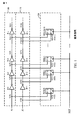
図3において、「内挿(interpolating、挿入)」フリップフロップADQ.nの組330が、D−QフリップフロップDQ.nの組320に加えて設けられている。各内挿フリップフロップADQ.nは、差動入力D/D´をサンプリングして差動出力Q/Q´を生成する。各ADQ.nへのD入力は遅延ライン300によって生成された信号A(n)に接続されており、他方、D´入力は遅延ライン300によって生成された信号A(n+1)に接続されている。ADQ.nへのD入力およびD´入力は、1単位(unit、ユニット)遅延(例えば1つのインバータ遅延)だけ間隔を置いた、相互に反転された形態であるものして観察される。図3に示されている実施形態では、ダミー負荷「LOAD」の例が遅延ライン310に設けられて遅延ライン310上の負荷を遅延ライン300上の負荷と平衡させる。
In FIG. 3, an “interpolating” flip-flop ADQ. n set 330 is a DQ flip-flop DQ. It is provided in addition to the n set 320. Each interpolation flip-flop ADQ. n samples the differential input D / D 'to generate a differential output Q / Q'. Each ADQ. The D input to n is connected to the signal A (n) generated by the
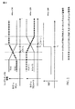
図4は、1つのフリップフロップADQ.mに接続されている差動入力信号のタイミングの例を、DQ.mおよびDQ.(m+1)に接続されている差動入力信号のタイミングと比較して、図示している。図4において、プロット400は図2に示されているのと同じ参照信号REFを示している。プロット410および420は、DQ.mおよびDQ.(m+1)の入力にそれぞれ接続されている差動信号A(m)/A´(m)およびA(m+1)/A´(m+1)を示している。プロット415は、ADQ.mの入力に接続されている差動入力信号A(m)/A(m+1)を示している。
FIG. 4 shows one flip-flop ADQ. An example of the timing of the differential input signal connected to m. m and DQ. It is shown in comparison with the timing of the differential input signal connected to (m + 1). In FIG. 4,
プロット410および420では、ゼロ交差時刻は、図2中のプロット210および220とそれぞれ同様に、t(m)およびt(m+1)であることが示されている。しかしながら、プロット415では、A(m)/A(m+1)についてのゼロ交差時刻はt´(m)であることが示されている。t´(m)はt(m)とt(m+1)との間に位置している。図示されている方式は、ADQ.mに対して、mTDより大きく(m+1)TDより小さな遅延を有する信号A/A´の「内挿された」形態を事実上もたらす。全ての信号について等しい立ち上がり時刻および立ち下がり時刻を仮定すると、そのような遅延はmTDと(m+1)TDとのほぼ中間にある。図3に示されているような複数のフリップフロップADQ.n 330を設けることによって、相応して、信号Aは、単位遅延(例えば1つのインバータの遅延TD)未満の時間軸分解能でサンプリングされ得る。
In
実施形態に応じて、元の信号に対する内挿信号の実際の遅延は、おおよそでmTDと(m+1)TDの中間値であり得ることに留意されたい。当業者は、内挿信号の実際の遅延に影響する要因は例えば素子相互の不一致および/またはプロセスのばらつきによりバッファの立ち上がり時刻および立ち下がり時刻における不均衡を含み得ることを理解するだろう。一実施形態では、立ち上がり時刻および立ち下がり時刻における不均衡に起因するTDCサンプリングのレベルのばらつきは、例えば立ち上がり時刻および立ち下がり時刻を監視するとともに最終的な測定値から予測される不正確さを相殺することによって、TDC測定値において考慮され得る。 Note that, depending on the embodiment, the actual delay of the interpolated signal relative to the original signal may be approximately between mT D and (m + 1) T D. One skilled in the art will appreciate that factors that affect the actual delay of the interpolated signal can include imbalances in the rise and fall times of the buffer due to, for example, device mismatches and / or process variations. In one embodiment, variations in TDC sampling levels due to imbalances in rise and fall times, for example, monitor rise and fall times and offset inaccuracies expected from final measurements. Can be taken into account in the TDC measurements.
当業者は、本開示の手法を依然使用しながら、図3に示されている実施形態に様々な修正がなされ得ることを理解するだろう。一実施形態では、バッファB.nの反転特性を補うために、フリップフロップDQ.nへの差動入力の極性が続けて反転され得る。 Those skilled in the art will appreciate that various modifications can be made to the embodiment shown in FIG. 3 while still using the techniques of this disclosure. In one embodiment, buffer B. In order to compensate the inversion characteristics of n, flip-flops DQ. The polarity of the differential input to n can subsequently be inverted.
当業者は、また、代替的な実施形態では、図1および図3に示されている反転バッファB.nに代えて非反転バッファが使用され得ることを理解するだろう。この場合、内挿D−QフリップフロップADQ.nへの入力D/D´は、信号A(n)/A´(n+1)に接続され得る。ここで、A(n)は、元の信号Aに対応する第1遅延ラインから引き出され、A´(n+1)は相補信号A´に対応する第2遅延ラインから引き出される。これらのおよび他の実施形態は本開示の範囲内にあることが企図されている。 Those skilled in the art will also recognize that, in alternative embodiments, the inverting buffers B.P. It will be appreciated that a non-inverting buffer may be used instead of n. In this case, the interpolation DQ flip-flop ADQ. The input D / D ′ to n can be connected to the signal A (n) / A ′ (n + 1). Here, A (n) is extracted from the first delay line corresponding to the original signal A, and A ′ (n + 1) is extracted from the second delay line corresponding to the complementary signal A ′. These and other embodiments are contemplated to be within the scope of this disclosure.
記述されているゼロ交差時刻が単にTDC量子化境界の近くのサンプリング機構の振る舞いを例証するために選択されていることに留意されたい。当業者は、ゼロ交差時刻が例証のみを目的として言及されていること、および典型的な差動入力信号Aが任意の期間にわたって、別のレベルに変化することなく概して一定であり得ることを理解するだろう。 Note that the zero-crossing times described are selected merely to illustrate the behavior of the sampling mechanism near the TDC quantization boundary. One skilled in the art understands that the zero crossing time is mentioned for illustrative purposes only, and that a typical differential input signal A can be generally constant over a period of time without changing to another level. will do.
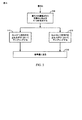
図5は本開示の方法に従ったステップを図示している。図5において、信号Aの遅延された形態A(n)およびA´(n)がステップ500で生成される。ステップ510において、A(n)/A´(n)がREFの立ち上がりエッジにおいてサンプリングされる。ステップ520において、A(n)/A(n+1)もREFの立ち上がりエッジにおいてサンプリングされる。ステップ530において、サンプルはさらなる処理のために復号器に提供される。当業者は、図5に図示されているステップが例証のみを目的としていること、および本開示の範囲を示されているいかなる具体的なステップにも限定することを意図されていないことを理解するだろう。
FIG. 5 illustrates steps according to the method of the present disclosure. In FIG. 5, delayed forms A (n) and A ′ (n) of signal A are generated at
1つ以上の例示的な実施形態において、記述されている機能は、ハードウェア、ソフトウェア、ファームウェア、またはそれらのあらゆる組合せにおいて実現され得る。ソフトウェアにおいて実現される場合、関数は1つまたは複数の指示またはコードとして、コンピュータ可読媒体上で格納または送信され得る。コンピュータ可読媒体は、コンピュータ記憶装置媒体、およびコンピュータ・プログラムのある位置から別の位置への移動を容易にするあらゆる媒体を含む通信媒体、の両方を含んでいる。記憶媒体は、コンピュータによってアクセスされることが可能なあらゆる利用可能な物理的媒体であり得る。限定ではなく例として、そのようなコンピュータ可読媒体は、RAM、ROM、EEPROM、CD−ROMまたは他の光学ディスク記憶装置、磁気ディスク記憶装置または他の磁気記憶装置、または命令またはデータ構造の形態の所望のプログラムコードを運ぶか格納するために使用されることが可能で且つコンピュータによってアクセスされることが可能な他のあらゆる媒体を具備し得る。また、あらゆる接続も当然、コンピュータ可読媒体と称される。例えば、ソフトウェアが、同軸ケーブル、光ファイバーケーブル、撚線対、ディジタル加入者線(DSL)、または赤外線、無線およびマイクロ波のような無線技術を使用して、ウェブサイト、サーバまたは他の遠隔ソースから送信される場合、この同軸ケーブル、光ファイバーケーブル、撚線対、DSL、または赤外線、無線およびマイクロ波のような無線技術は、媒体の定義に含まれている。本明細書において使用されているディスク(disk)とディスク(disc)は、コンパクトディスク(CD)、レーザーディスク(登録商標)、光ディスク、ディジタル多用途ディスク(DVD)、フロッピー(登録商標)ディスクおよびブルーレイディスクを含んでいる。ここで、ディスク(disk)は通常磁気的にデータを再生し、他方、ディスク(disc)はレーザーでデータを光学的に再生する。上記のものの組合せもコンピュータ可読媒体の範囲に含まれるべきである。 In one or more exemplary embodiments, the functions described may be implemented in hardware, software, firmware, or any combination thereof. If implemented in software, the functions may be stored on or transmitted over as one or more instructions or code on a computer-readable medium. Computer-readable media includes both computer storage media and communication media including any medium that facilitates transfer of a computer program from one position to another. A storage media may be any available physical media that can be accessed by a computer. By way of example, and not limitation, such computer-readable media can be in the form of RAM, ROM, EEPROM, CD-ROM or other optical disk storage, magnetic disk storage or other magnetic storage, or instructions or data structures. Any other medium that can be used to carry or store the desired program code and that can be accessed by the computer can be provided. Any connection is of course also referred to as a computer-readable medium. For example, software can be used from a website, server, or other remote source using coaxial cable, fiber optic cable, twisted pair, digital subscriber line (DSL), or wireless technologies such as infrared, wireless and microwave. When transmitted, this coaxial cable, fiber optic cable, twisted wire pair, DSL, or wireless technologies such as infrared, wireless and microwave are included in the definition of the media. Discs and discs used herein are compact disc (CD), laser disc (registered trademark), optical disc, digital versatile disc (DVD), floppy disc (registered trademark) and Blu-ray disc. Includes discs. Here, the disk normally reproduces data magnetically, while the disk (disc) optically reproduces data with a laser. Combinations of the above should also be included within the scope of computer-readable media.
コンピュータ・プログラム製品のコンピュータ可読媒体と関連している命令またはコードは、例えば1つ以上のディジタル信号プロセッサ(DSP)、汎用マイクロプロセッサ、ASIC、FPGA、または他の等価な集積論理回路またはディスクリート型論理回路のような1つ以上のプロセッサによってコンピュータによって実行され得る。 The instructions or code associated with the computer readable medium of the computer program product may be, for example, one or more digital signal processors (DSPs), general purpose microprocessors, ASICs, FPGAs, or other equivalent integrated logic or discrete logic. It can be executed by a computer by one or more processors, such as circuits.
この明細書、および請求項では、要素が別の要素に「接続された(connect)」または「接続された(couple」と称されている場合、それは、要素は、直接別の要素に接続されることが可能であり、または介在する要素が存在し得る。対照的に、要素が別の要素に「直接接続された(connect)」または「直接接続された(couple)」と称されている場合、介在する要素は存在しない。 In this specification, and in the claims, when an element is referred to as “connect” or “coupled” to another element, it means that the element is directly connected to another element. Or there may be intervening elements, in contrast, an element is referred to as being “directly connected” or “coupled” to another element In the case, there are no intervening elements.
多くの側面および例が記述された。しかしながら、これらの例に対する様々な修正が可能であり、また、本明細書において示されている原理は、別の側面に対して同様に適用され得る。これらの側面および他の側面は次の請求項の範囲内にある。 Many aspects and examples have been described. However, various modifications to these examples are possible, and the principles presented herein can be applied to other aspects as well. These and other aspects are within the scope of the following claims.
Claims (28)
A(m)と信号B[A(m)]との間の時刻の差分をサンプリングするためのサンプリング機構であって、B[A(m)]はAに対して少なくとも1遅延単位だけ遅延されている、サンプリング機構と、
を具備する時間ディジタル・コンバータ(TDC)。 A delay line for generating at least one delayed form A (m) of signal A, wherein A (m) is delayed by m delay units relative to A;
A sampling mechanism for sampling a time difference between A (m) and a signal B [A (m)], wherein B [A (m)] is delayed with respect to A by at least one delay unit. A sampling mechanism,
A time digital converter (TDC).
請求項1のTDC。 Signal B [A (m)] is signal A (m + 1), and A (m + 1) is delayed with respect to A by m + 1 delay units.
The TDC of claim 1.
請求項2のTDC。 Each delay unit corresponds to one unit buffer delay,
The TDC of claim 2.
請求項3のTDC。 The unit buffer is one inverter;
The TDC of claim 3.
請求項1のTDC。 The sampling mechanism is a differential DQ flip-flop, the signal A (n) is connected to the D input of the DQ flip-flop, and the signal B is D ′ of the DQ flip-flop. Connected to the input,
The TDC of claim 1.
請求項5のTDC。 The flip-flop samples the voltage polarity of the differential input D / D ′;
The TDC of claim 5.
請求項5のTDC。 The delay line further generates a plurality of delayed forms A (n) of the signal A, and the sampling mechanism further calculates a difference between each signal A (n) and the corresponding signal B [A (n)]. Sampling, each B [A (n)] is delayed by at least one delay unit relative to the corresponding A (n);
The TDC of claim 5.
請求項7のTDC。 The signal A ′ complementary to the signal A is further provided with a complementary delay line for generating a plurality of delayed forms A ′ (n), wherein the TDC corresponds to each signal A (n). A plurality of differential DQ flip-flops for sampling the difference between
The TDC of claim 7.
請求項8のTDC。 The complementary delay line is connected to at least one load for balancing the delay line load with the complementary delay line load;
The TDC of claim 8.
A(m)と信号B[A(m)]との間の時刻の差分をサンプリングすることであって、B[A(m)]はAに対して少なくとも1遅延単位だけ遅延されている、サンプリングすることと、
を具備する、時間間隔をディジタル表現に変換するための方法。 Generating at least one delayed form A (m) of signal A, wherein A (m) is delayed with respect to A by m delay units;
Sampling the time difference between A (m) and signal B [A (m)], B [A (m)] being delayed by at least one delay unit relative to A; Sampling,
A method for converting a time interval into a digital representation comprising:
請求項10の方法。 Signal B [A (m)] is signal A (m + 1), and A (m + 1) is delayed with respect to A by m + 1 delay units.
The method of claim 10.
請求項11の方法。 Each delay unit corresponds to one unit buffer delay,
The method of claim 11.
請求項12の方法。 The unit buffer is one inverter;
The method of claim 12.
請求項10の方法。 The sampling is performed by a differential DQ flip-flop, the signal A (n) is connected to the D input of the DQ flip-flop, and the signal B is connected to the DQ flip-flop. Connected to the D 'input,
The method of claim 10.
請求項14の方法。 The flip-flop samples the voltage polarity of the differential input D / D ′;
The method of claim 14.
請求項14の方法。 Further comprising generating a plurality of delayed forms A (n) of the signal A, wherein the sampling mechanism further determines a difference between each signal A (n) and the corresponding signal B [A (n)]. Sampling, each B [A (n)] is delayed by at least one delay unit relative to the corresponding A (n);
The method of claim 14.
請求項16の方法。 Further comprising generating a plurality of delayed forms A ′ (n) complementary to the signal A, and sampling the difference between each signal A (n) and the corresponding signal A ′ (n). Further comprising:
The method of claim 16.
請求項17の方法。 Further comprising connecting at least one load to a delay line for generating the signal A ′ (n) to balance the delay line with a load of the delay line for generating a plurality of signals A (n). To
The method of claim 17.
A(m)と信号B[A(m)]との間の時刻の差分をサンプリングするための手段であって、B[A(m)]はAに対して少なくとも1遅延単位だけ遅延されている、サンプリングするための手段と、
を具備する、時間ディジタル・コンバータ(TDC)。 Means for generating at least one delayed form A (m) of signal A, wherein A (m) is delayed with respect to A by m delay units. When,
A means for sampling the time difference between A (m) and signal B [A (m)], B [A (m)] being delayed by at least one delay unit with respect to A Means for sampling, and
A time digital converter (TDC).
請求項19のTDC。 Signal B [A (m)] is signal A (m + 1), and A (m + 1) is delayed with respect to A by m + 1 delay units.
The TDC of claim 19.
請求項20のTDC。 Each delay unit corresponds to one unit buffer delay,
21. The TDC of claim 20.
請求項21のTDC。 The unit buffer is one inverter;
The TDC of claim 21.
請求項19のTDC。 The means for sampling the difference comprises a DQ flip-flop, the signal A (n) is connected to the D input of the DQ flip-flop, and the signal B is the DQ flip-flop. Connected to the D 'input of
The TDC of claim 19.
コンピュータに、A(m)と信号B[A(m)]との間の時刻の差分をサンプリングさせるためのコードであって、B[A(m)]はAに対して少なくとも1遅延単位だけ遅延されている、サンプリングさせるためのコードと、
を具備するコンピュータ可読媒体を具備する、時間間隔をディジタル表現に変換するためのコンピュータ・プログラム製品。 Code for causing a computer to generate at least one delayed form A (m) of a signal A, wherein A (m) is delayed by m delay units relative to A And a code for
A code for causing a computer to sample a time difference between A (m) and a signal B [A (m)], where B [A (m)] is at least one delay unit relative to A Delayed code to sample, and
A computer program product for converting a time interval into a digital representation comprising a computer readable medium comprising:
前記コンピュータ可読媒体が、A(m+1)をAに対してm+1遅延単位だけ遅延させるためのコードをさらに具備する、
請求項24のコンピュータ・プログラム製品。 Signal B [A (m)] is signal A (m + 1),
The computer-readable medium further comprises code for delaying A (m + 1) with respect to A by m + 1 delay units;
25. The computer program product of claim 24.
請求項25のコンピュータ・プログラム製品。 Each delay unit corresponds to one unit buffer delay,
26. The computer program product of claim 25.
前記サンプリングを差動型D−Qフリップフロップによって実行させ、
前記信号A(n)を前記D−QフリップフロップのD入力に接続し、
前記信号Bを前記D−QフリップフロップのD´入力に接続する、
ためのコードを具備する、
請求項24のコンピュータ・プログラム製品。 Code for causing the computer to sample the difference is:
The sampling is performed by a differential DQ flip-flop;
Connecting the signal A (n) to the D input of the DQ flip-flop;
Connecting the signal B to the D 'input of the DQ flip-flop;
A code for
25. The computer program product of claim 24.
コンピュータに、信号Aの複数の遅延された形態A(n)を生成させるためのコードであって、各B[A(n)]が前記対応するA(n)に対して少なくとも1遅延単位だけ遅延されている、生成させるためのコードをさらに具備する、
請求項27のコンピュータ・プログラム製品。 The computer readable medium is
Code for causing a computer to generate a plurality of delayed forms A (n) of signal A, wherein each B [A (n)] is at least one delay unit relative to the corresponding A (n) Further comprising delayed code to generate,
28. The computer program product of claim 27.
Applications Claiming Priority (3)
| Application Number | Priority Date | Filing Date | Title |
|---|---|---|---|
| US12/041,403 | 2008-03-03 | ||
| US12/041,403 US7808418B2 (en) | 2008-03-03 | 2008-03-03 | High-speed time-to-digital converter |
| PCT/US2009/035908 WO2009111491A1 (en) | 2008-03-03 | 2009-03-03 | High-speed time-to-digital converter |
Publications (2)
| Publication Number | Publication Date |
|---|---|
| JP2011517160A true JP2011517160A (en) | 2011-05-26 |
| JP2011517160A5 JP2011517160A5 (en) | 2011-07-07 |
Family
ID=40666856
Family Applications (1)
| Application Number | Title | Priority Date | Filing Date |
|---|---|---|---|
| JP2010549822A Pending JP2011517160A (en) | 2008-03-03 | 2009-03-03 | High-speed digital converter |
Country Status (7)
| Country | Link |
|---|---|
| US (1) | US7808418B2 (en) |
| EP (1) | EP2250732A1 (en) |
| JP (1) | JP2011517160A (en) |
| KR (1) | KR20100130205A (en) |
| CN (1) | CN102089983A (en) |
| TW (1) | TW200943734A (en) |
| WO (1) | WO2009111491A1 (en) |
Families Citing this family (17)
| Publication number | Priority date | Publication date | Assignee | Title |
|---|---|---|---|---|
| US8283960B2 (en) * | 2009-04-27 | 2012-10-09 | Oracle America, Inc. | Minimal bubble voltage regulator |
| US8179165B2 (en) * | 2009-04-27 | 2012-05-15 | Oracle America, Inc. | Precision sampling circuit |
| US8198931B2 (en) * | 2009-04-27 | 2012-06-12 | Oracle America, Inc. | Fine grain timing |
| US8242823B2 (en) | 2009-04-27 | 2012-08-14 | Oracle America, Inc. | Delay chain initialization |
| EP2717471A4 (en) * | 2011-05-27 | 2015-04-01 | Aika Design Inc | Signal conversion circuit, pll circuit, delay adjustment circuit, and phase control circuit |
| US20120319741A1 (en) * | 2011-06-17 | 2012-12-20 | Texas Instruments Incorporated | Reduced crosstalk wiring delay effects through the use of a checkerboard pattern of inverting and noninverting repeaters |
| KR101214976B1 (en) * | 2011-11-01 | 2012-12-24 | 포항공과대학교 산학협력단 | Noise shaping time digital converter using a delta sigma modulating method |
| KR101797625B1 (en) | 2012-02-16 | 2017-11-15 | 한국전자통신연구원 | Low-power high-resolution time-to -digital converter |
| US9337997B2 (en) * | 2013-03-07 | 2016-05-10 | Qualcomm Incorporated | Transcoding method for multi-wire signaling that embeds clock information in transition of signal state |
| JP5747070B2 (en) * | 2013-12-07 | 2015-07-08 | 株式会社アイカデザイン | Phase-locked loop circuit and oscillation method |
| US9606228B1 (en) | 2014-02-20 | 2017-03-28 | Banner Engineering Corporation | High-precision digital time-of-flight measurement with coarse delay elements |
| KR102154189B1 (en) | 2014-12-01 | 2020-09-09 | 삼성전자 주식회사 | Time-to-Digital Converter using a Stochastic Phase Interpolation |
| KR101621853B1 (en) | 2014-12-26 | 2016-05-17 | 연세대학교 산학협력단 | Data transmitter, data receiver and smart device utilizing the same |
| CN106354001B (en) * | 2016-08-31 | 2019-03-12 | 中国科学院上海高等研究院 | Time-to-digital conversion circuit |
| US10848138B2 (en) | 2018-09-21 | 2020-11-24 | Taiwan Semiconductor Manufacturing Co., Ltd. | Method and apparatus for precision phase skew generation |
| US10928447B2 (en) | 2018-10-31 | 2021-02-23 | Taiwan Semiconductor Manufacturing Co., Ltd. | Built-in self test circuit for measuring phase noise of a phase locked loop |
| US20240045382A1 (en) * | 2022-08-02 | 2024-02-08 | Apple Inc. | Multi-Chain Measurement Circuit |
Citations (7)
| Publication number | Priority date | Publication date | Assignee | Title |
|---|---|---|---|---|
| JPS61227422A (en) * | 1985-03-30 | 1986-10-09 | Toshiba Corp | Phase comparator circuit |
| JPH03125514A (en) * | 1989-10-11 | 1991-05-28 | Nippon Soken Inc | Pulse phase difference detection circuit and physical quantity detector provided with the detection circuit |
| US5796682A (en) * | 1995-10-30 | 1998-08-18 | Motorola, Inc. | Method for measuring time and structure therefor |
| WO2001037428A1 (en) * | 1999-11-18 | 2001-05-25 | Neomicros Inc. | Zero-delay buffer circuit for a spread spectrum clock system and method therefor |
| JP2002076886A (en) * | 2000-06-30 | 2002-03-15 | Texas Instruments Inc | Digital fractional phase detector |
| US20060103566A1 (en) * | 2004-11-18 | 2006-05-18 | Texas Instruments Incorporated | Circuit for high-resolution phase detection in a digital RF processor |
| US20070273569A1 (en) * | 2006-05-26 | 2007-11-29 | Chia-Liang Lin | High resolution time-to-digital converter and method thereof |
Family Cites Families (7)
| Publication number | Priority date | Publication date | Assignee | Title |
|---|---|---|---|---|
| DE69719296T2 (en) * | 1996-11-21 | 2003-09-04 | Matsushita Electric Industrial Co., Ltd. | A / D converter and A / D conversion method |
| JP3380206B2 (en) * | 1999-03-31 | 2003-02-24 | 沖電気工業株式会社 | Internal clock generation circuit |
| JP4397488B2 (en) * | 1999-12-17 | 2010-01-13 | Nsc株式会社 | Oversampling circuit and digital-analog converter |
| US7045098B2 (en) * | 2001-02-02 | 2006-05-16 | James Matthew Stephens | Apparatus and method for removing interfering substances from a urine sample using a chemical oxidant |
| DE10143770B4 (en) * | 2001-09-06 | 2006-03-16 | Infineon Technologies Ag | amplifier circuit |
| CA2474111A1 (en) * | 2004-07-08 | 2006-01-08 | Gordon John Allan | Method and apparatus for mixed-signal dll/pll as usefull in timing manipulation |
| US7427940B2 (en) * | 2006-12-29 | 2008-09-23 | Texas Instruments Incorporated | Time-to-digital converter with non-inverting buffers, transmission gates and non-linearity corrector, SOC including such converter and method of phase detection for use in synthesizing a clock signal |
-
2008
- 2008-03-03 US US12/041,403 patent/US7808418B2/en active Active
-
2009
- 2009-03-03 WO PCT/US2009/035908 patent/WO2009111491A1/en active Application Filing
- 2009-03-03 CN CN2009801073613A patent/CN102089983A/en active Pending
- 2009-03-03 KR KR1020107021650A patent/KR20100130205A/en not_active Application Discontinuation
- 2009-03-03 TW TW098106873A patent/TW200943734A/en unknown
- 2009-03-03 EP EP09716634A patent/EP2250732A1/en not_active Withdrawn
- 2009-03-03 JP JP2010549822A patent/JP2011517160A/en active Pending
Patent Citations (8)
| Publication number | Priority date | Publication date | Assignee | Title |
|---|---|---|---|---|
| JPS61227422A (en) * | 1985-03-30 | 1986-10-09 | Toshiba Corp | Phase comparator circuit |
| JPH03125514A (en) * | 1989-10-11 | 1991-05-28 | Nippon Soken Inc | Pulse phase difference detection circuit and physical quantity detector provided with the detection circuit |
| US5796682A (en) * | 1995-10-30 | 1998-08-18 | Motorola, Inc. | Method for measuring time and structure therefor |
| WO2001037428A1 (en) * | 1999-11-18 | 2001-05-25 | Neomicros Inc. | Zero-delay buffer circuit for a spread spectrum clock system and method therefor |
| JP2003514479A (en) * | 1999-11-18 | 2003-04-15 | ネオマイクロス インコーポレイテッド | Zero delay buffer circuit and method for spread spectrum clocking system |
| JP2002076886A (en) * | 2000-06-30 | 2002-03-15 | Texas Instruments Inc | Digital fractional phase detector |
| US20060103566A1 (en) * | 2004-11-18 | 2006-05-18 | Texas Instruments Incorporated | Circuit for high-resolution phase detection in a digital RF processor |
| US20070273569A1 (en) * | 2006-05-26 | 2007-11-29 | Chia-Liang Lin | High resolution time-to-digital converter and method thereof |
Non-Patent Citations (1)
| Title |
|---|
| JPN6012023465; P.M.Levineほか: '「High-resolution flash time-to-digital conversion and calibration for system-on-chip testing」' IEE PROCEEDINGS: COMPUTERS AND DIGITAL TECHNIQUES Vol.152,No.3, 200505, pp415-426, IEE * |
Also Published As
| Publication number | Publication date |
|---|---|
| KR20100130205A (en) | 2010-12-10 |
| CN102089983A (en) | 2011-06-08 |
| TW200943734A (en) | 2009-10-16 |
| US20090219187A1 (en) | 2009-09-03 |
| EP2250732A1 (en) | 2010-11-17 |
| WO2009111491A1 (en) | 2009-09-11 |
| US7808418B2 (en) | 2010-10-05 |
Similar Documents
| Publication | Publication Date | Title |
|---|---|---|
| JP2011517160A (en) | High-speed digital converter | |
| US10263606B2 (en) | On-chip waveform measurement | |
| JP2011517160A5 (en) | ||
| TWI542156B (en) | Circuit and method for clock data recovery and circuit and method for analyzing equalized signal | |
| US8054116B2 (en) | Threshold dithering for time-to-digital converters | |
| TWI333548B (en) | ||
| US7590041B2 (en) | Playback signal processing device | |
| WO2016024439A1 (en) | Analog-digital converter, electronic device, and control method for analog-digital converter | |
| JP5883101B1 (en) | Data recovery circuit | |
| JP5935824B2 (en) | D / A converter | |
| JPH0233770A (en) | Decoding method | |
| US8594254B2 (en) | Waveform interpolator architecture for accurate timing recovery based on up-sampling technique | |
| JP2017046058A (en) | AD converter, analog front end, and sensor system | |
| TWI568195B (en) | Time-to-digital converter | |
| RU2311731C1 (en) | Composite fast-response analog-to-digital converter | |
| US9052991B2 (en) | System and method for audio sample rate conversion | |
| JP2015005812A (en) | Receiving circuit and receiving method | |
| Dehghani et al. | Time‐to‐digital convertor based on resolution control | |
| KR20080032302A (en) | Method for calculating integrated value of pulse input signal and integrator for the method | |
| US10056887B2 (en) | Apparatus and method for controlling a delay circuit | |
| Mabrouk | Translation invariance when utility streams are infinite and unbounded | |
| Wang et al. | A 5.4 ps resolution TDC design with anti-PVT-variation mechanism using 90-nm CMOS process | |
| Wang et al. | An Improved Digital Servo Burst Signal Sampling Model for Disk Drives | |
| RU2467371C1 (en) | Direct coding interpolator for measurement of time intervals | |
| TW201318352A (en) | Successive approximation analog to digital converter with a direct switching technique for capacitor array through comparator output and method thereof |
Legal Events
| Date | Code | Title | Description |
|---|---|---|---|
| A521 | Written amendment |
Free format text: JAPANESE INTERMEDIATE CODE: A523 Effective date: 20110512 |
|
| A131 | Notification of reasons for refusal |
Free format text: JAPANESE INTERMEDIATE CODE: A131 Effective date: 20120515 |
|
| A02 | Decision of refusal |
Free format text: JAPANESE INTERMEDIATE CODE: A02 Effective date: 20121016 |