JP2011505708A - Active material device having confinement layer - Google Patents
Active material device having confinement layer Download PDFInfo
- Publication number
- JP2011505708A JP2011505708A JP2010536925A JP2010536925A JP2011505708A JP 2011505708 A JP2011505708 A JP 2011505708A JP 2010536925 A JP2010536925 A JP 2010536925A JP 2010536925 A JP2010536925 A JP 2010536925A JP 2011505708 A JP2011505708 A JP 2011505708A
- Authority
- JP
- Japan
- Prior art keywords
- active material
- confinement layer
- layer
- temperature
- electrode
- Prior art date
- Legal status (The legal status is an assumption and is not a legal conclusion. Google has not performed a legal analysis and makes no representation as to the accuracy of the status listed.)
- Pending
Links
Images


Classifications
-
- H—ELECTRICITY
- H10—SEMICONDUCTOR DEVICES; ELECTRIC SOLID-STATE DEVICES NOT OTHERWISE PROVIDED FOR
- H10N—ELECTRIC SOLID-STATE DEVICES NOT OTHERWISE PROVIDED FOR
- H10N70/00—Solid-state devices without a potential-jump barrier or surface barrier, and specially adapted for rectifying, amplifying, oscillating or switching
- H10N70/20—Multistable switching devices, e.g. memristors
- H10N70/231—Multistable switching devices, e.g. memristors based on solid-state phase change, e.g. between amorphous and crystalline phases, Ovshinsky effect
-
- H—ELECTRICITY
- H10—SEMICONDUCTOR DEVICES; ELECTRIC SOLID-STATE DEVICES NOT OTHERWISE PROVIDED FOR
- H10N—ELECTRIC SOLID-STATE DEVICES NOT OTHERWISE PROVIDED FOR
- H10N70/00—Solid-state devices without a potential-jump barrier or surface barrier, and specially adapted for rectifying, amplifying, oscillating or switching
- H10N70/011—Manufacture or treatment of multistable switching devices
- H10N70/021—Formation of the switching material, e.g. layer deposition
- H10N70/026—Formation of the switching material, e.g. layer deposition by physical vapor deposition, e.g. sputtering
-
- H—ELECTRICITY
- H10—SEMICONDUCTOR DEVICES; ELECTRIC SOLID-STATE DEVICES NOT OTHERWISE PROVIDED FOR
- H10N—ELECTRIC SOLID-STATE DEVICES NOT OTHERWISE PROVIDED FOR
- H10N70/00—Solid-state devices without a potential-jump barrier or surface barrier, and specially adapted for rectifying, amplifying, oscillating or switching
- H10N70/011—Manufacture or treatment of multistable switching devices
- H10N70/041—Modification of the switching material, e.g. post-treatment, doping
-
- H—ELECTRICITY
- H10—SEMICONDUCTOR DEVICES; ELECTRIC SOLID-STATE DEVICES NOT OTHERWISE PROVIDED FOR
- H10N—ELECTRIC SOLID-STATE DEVICES NOT OTHERWISE PROVIDED FOR
- H10N70/00—Solid-state devices without a potential-jump barrier or surface barrier, and specially adapted for rectifying, amplifying, oscillating or switching
- H10N70/011—Manufacture or treatment of multistable switching devices
- H10N70/061—Patterning of the switching material
- H10N70/068—Patterning of the switching material by processes specially adapted for achieving sub-lithographic dimensions, e.g. using spacers
-
- H—ELECTRICITY
- H10—SEMICONDUCTOR DEVICES; ELECTRIC SOLID-STATE DEVICES NOT OTHERWISE PROVIDED FOR
- H10N—ELECTRIC SOLID-STATE DEVICES NOT OTHERWISE PROVIDED FOR
- H10N70/00—Solid-state devices without a potential-jump barrier or surface barrier, and specially adapted for rectifying, amplifying, oscillating or switching
- H10N70/801—Constructional details of multistable switching devices
- H10N70/821—Device geometry
- H10N70/826—Device geometry adapted for essentially vertical current flow, e.g. sandwich or pillar type devices
-
- H—ELECTRICITY
- H10—SEMICONDUCTOR DEVICES; ELECTRIC SOLID-STATE DEVICES NOT OTHERWISE PROVIDED FOR
- H10N—ELECTRIC SOLID-STATE DEVICES NOT OTHERWISE PROVIDED FOR
- H10N70/00—Solid-state devices without a potential-jump barrier or surface barrier, and specially adapted for rectifying, amplifying, oscillating or switching
- H10N70/801—Constructional details of multistable switching devices
- H10N70/881—Switching materials
- H10N70/882—Compounds of sulfur, selenium or tellurium, e.g. chalcogenides
- H10N70/8825—Selenides, e.g. GeSe
-
- H—ELECTRICITY
- H10—SEMICONDUCTOR DEVICES; ELECTRIC SOLID-STATE DEVICES NOT OTHERWISE PROVIDED FOR
- H10N—ELECTRIC SOLID-STATE DEVICES NOT OTHERWISE PROVIDED FOR
- H10N70/00—Solid-state devices without a potential-jump barrier or surface barrier, and specially adapted for rectifying, amplifying, oscillating or switching
- H10N70/801—Constructional details of multistable switching devices
- H10N70/881—Switching materials
- H10N70/882—Compounds of sulfur, selenium or tellurium, e.g. chalcogenides
- H10N70/8828—Tellurides, e.g. GeSbTe
-
- H—ELECTRICITY
- H10—SEMICONDUCTOR DEVICES; ELECTRIC SOLID-STATE DEVICES NOT OTHERWISE PROVIDED FOR
- H10N—ELECTRIC SOLID-STATE DEVICES NOT OTHERWISE PROVIDED FOR
- H10N70/00—Solid-state devices without a potential-jump barrier or surface barrier, and specially adapted for rectifying, amplifying, oscillating or switching
- H10N70/801—Constructional details of multistable switching devices
- H10N70/881—Switching materials
- H10N70/884—Other compounds of groups 13-15, e.g. elemental or compound semiconductors
Abstract
活物質電子素子が、閉じ込め層とともに説明される。素子は、上部及び下部電極と電気的に接続した活性カルコゲニド材料、ニクティド材料又は相変化物質を含んでいる。閉じ込め層は、製造又は動作の間に素子が高温に暴露されたときに活物質から揮発した物質の脱出を防ぐ活物質上に形成された閉じ込め層を含んでいる。閉じ込め層は、処理環境又は周囲の環境における反応種から保護することによって、活物質の化学汚染をさらに防いでいる。閉じ込め層と、活物質と閉じ込め層との間に形成された中間層とは、活物質の揮発を防ぐように十分な低温で形成される。一旦閉じ込め層が形成されると、素子は、活物質の組成又は構造の完全性を損なうことなく高温環境又は化学侵食環境のもとに置くことができる。閉じ込め層を含むことにより、素子の動作回数寿命が2の次数の強度を超えて延びることが示される。 An active material electronic device is described with a confinement layer. The device includes an active chalcogenide material, nictide material or phase change material in electrical connection with the upper and lower electrodes. The confinement layer includes a confinement layer formed on the active material that prevents escape of the volatilized material from the active material when the device is exposed to high temperatures during manufacture or operation. The confinement layer further prevents chemical contamination of the active material by protecting it from reactive species in the processing environment or the surrounding environment. The confinement layer and the intermediate layer formed between the active material and the confinement layer are formed at a sufficiently low temperature so as to prevent volatilization of the active material. Once the confinement layer is formed, the device can be placed under a high temperature or chemical erosion environment without compromising the integrity of the active material composition or structure. Inclusion of the confinement layer indicates that the operating lifetime of the device extends beyond the second order intensity.
Description
この発明は、高温における処理又は動作で蒸発しやすい揮発性活物質を有する電子素子に関する。詳しくは、この発明は、製造又は動作の間に活物質の蒸発を防止するように意図された保護ステップを含む電子素子の製造方法に関する。詳しくは、この発明は、後続する高温処理又は動作の間において揮発性活物質を閉じ込める閉じ込め層の低温堆積を含むカルコゲニド又は相変化メモリ又はスイッチング素子の製造方法に関する。 The present invention relates to an electronic device having a volatile active material that easily evaporates by processing or operation at a high temperature. In particular, the present invention relates to a method of manufacturing an electronic device that includes a protection step intended to prevent evaporation of the active material during manufacture or operation. In particular, the present invention relates to a method of manufacturing a chalcogenide or phase change memory or switching element that includes low temperature deposition of a confinement layer that confines volatile active material during subsequent high temperature processing or operation.
カルコゲニド材料は、スイッチ、メモリ、ロジック及びプロセッシング機能を有する新たな種類の市販の電子材料である。カルコゲニド材料の基本原則は、1960年代にS.R.オブシンスキー(S.R.Ovshinsky)によって開発され、それ以降オブシンスキー及び世界中で多大な取り組みがなされ、基礎となる科学の進歩とカルコゲニド材料の応用分野の展開を導いてきた。 Chalcogenide materials are a new class of commercially available electronic materials with switch, memory, logic and processing functions. The basic principles of chalcogenide materials were found in S. R. Developed by S. R. Ovshinsky, a great deal of effort has been made since then and has led to the advancement of the underlying science and the application of chalcogenide materials.
カルコゲニド素子に関する早期の研究は、電気スイッチ動作を明らかにしたが、この動作は、抵抗状態から導通状態へのスイッチングが活カルコゲニド材料の閾値電圧以上の電圧を印加することで引き起こされる。この効果は、オボニック閾値スイッチ(Ovonic Threshold Switch;OTS)の基礎となるものであり、カルコゲニド材料の重要な実用上の特徴となっている。OTSは、多数の動作回数にわたって超高速スイッチングを高度に再現可能である。OTSの基本原則と動作の特徴は、例えば米国特許3271591、5543737、5694146及び5757446で提供され、これらの開示は参照によって組み込まれるとともに、S.R.Ovshinskyによる「無秩序結晶における逆転電気スイッチング現象(Reversible Electrical Switching in Disordered Structures)」、Physical Review Letters、Vol.21、p.1450−1453(1969)、S.R.Ovshinsky及びH.Frizscheによる「スイッチング、メモリ及びイメージングアプリケーションに用いるアモルファス半導体(Amorphous Semiconductors for Switching,Memory,and Imaging Applications)」、IEEE Transactions on Electronic Devices、Vol.ED−20、p.91−105(1973)を含むいくつかの学術論文が、参照によって組み込まれる。 Early work on chalcogenide devices revealed electrical switch operation, which is caused by applying a voltage above the threshold voltage of the active chalcogenide material for switching from the resistive state to the conducting state. This effect is the basis of the Ovonic Threshold Switch (OTS) and is an important practical feature of chalcogenide materials. OTS is highly reproducible for ultra-fast switching over many operations. The basic principles and operational features of OTS are provided, for example, in U.S. Pat. Nos. 3,271,591, 5543737, 5694146, and 5757446, the disclosures of which are incorporated by reference and described in S.C. R. Ovshinsky, “Reversible Electrical Switching in Disordered Structures”, Physical Review Letters, Vol. 21, p. 1450-1453 (1969), S.A. R. Ovshinsky and H.C. Fritzche's "Amorphous Semiconductors for Switching, Memory and Imaging Applications", IEEE Transactions on Electronics. ED-20, p. Several academic papers, including 91-105 (1973), are incorporated by reference.
カルコゲニド材料の他の重要な応用は、電気及び光学メモリ素子である。カルコゲニドメモリ素子の一つの種類は、メモリ動作の基礎として活カルコゲニド材料で得られる広範囲の抵抗値を利用している。各抵抗値は、カルコゲニド材料の異なる構造状態に相当し、一つ以上の状態が選択され、動作メモリ状態を規定するのに使用されることができる。カルコゲニド材料は、結晶状態または結晶相とアモルファス状態又はアモルファス相を示す。カルコゲニド材料の異なる構造状態は、カルコゲニド材料の一定の体積又は領域における結晶相とアモルファス相の相対的な性質の観点において異なっている。抵抗値の範囲は、カルコゲニド材料のセット状態とリセット状態によって囲まれている。セット状態は低抵抗構造状態であり、電気的性質は主にカルコゲニド材料の結晶部分によって支配され、リセット状態は高抵抗構造状態であり、電気的性質は主にカルコゲニド材料のアモルファス部分によって支配されている。 Other important applications of chalcogenide materials are electrical and optical memory elements. One type of chalcogenide memory element utilizes a wide range of resistance values obtained with active chalcogenide materials as the basis for memory operation. Each resistance value corresponds to a different structural state of the chalcogenide material and one or more states can be selected and used to define the operating memory state. Chalcogenide materials exhibit a crystalline state or crystalline phase and an amorphous state or amorphous phase. The different structural states of chalcogenide materials differ in terms of the relative properties of the crystalline and amorphous phases in a certain volume or region of the chalcogenide material. The range of the resistance value is surrounded by the set state and the reset state of the chalcogenide material. The set state is a low resistance structural state, the electrical properties are mainly governed by the crystalline portion of the chalcogenide material, the reset state is the high resistance structural state, and the electrical properties are primarily governed by the amorphous portion of the chalcogenide material. Yes.
カルコゲニドメモリ材料の各メモリ状態は、抵抗値の区別される範囲に相当し、各メモリの抵抗値は、唯一の情報内容を表している。動作においては、カルコゲニド材料は、エネルギーを供給することによって特定のメモリ状態にプログラムされ、最も一般的には適切な振幅と持続時間を有する電流パルスによって、格納する特定の情報コンテンツに付随する抵抗値を有する構造状態にカルコゲニド材料を変換する。カルコゲニド材料に供給するエネルギー量を制御することによって、材料のある体積における結晶相とアモルファス相の相対比を制御し、カルコゲニド材料の構造(メモリ)状態を制御することができる。 Each memory state of the chalcogenide memory material corresponds to a distinguished range of resistance values, and the resistance value of each memory represents a unique information content. In operation, a chalcogenide material is programmed to a specific memory state by supplying energy, and most commonly a resistance value associated with the specific information content to be stored by a current pulse having the proper amplitude and duration. The chalcogenide material is converted to a structural state having By controlling the amount of energy supplied to the chalcogenide material, the relative ratio between the crystalline phase and the amorphous phase in a certain volume of the material can be controlled, and the structure (memory) state of the chalcogenide material can be controlled.
各メモリ状態は、その状態に特徴的な電流パルスを供給することによってプログラムすることができ、各状態は、抵抗を測定することによって非破壊的に特定又は読み出しができる。異なった状態の間のプログラミングは完全に可逆的であり、メモリ素子は多数の繰り返しの動作回数にわたって書き込みと読み出しができ、堅牢で信頼できる動作を提供する。カルコゲニド材料の可変抵抗メモリ機能は、OUM(Ovonic Universal(又はUnified) Memory)素子において目下開発中であり、間もなく市販される予定である。OUM型素子の基本原則と動作は、例えば米国特許6859390、6774387、6687153及び6314014に開示され、これらの開示は、参照により組み込まれ、ピロバナ他(Pirovana et al.)による「カルコゲニド材料における低電界アモルファス相抵抗及び閾値電圧ドリフト(Low Field Amorphous State Resistance and Threshold Voltage Drift in Chalcogenide Materials)」、IEEE Transactions on Electron Devices、Vol.51、p.714−719(2004)及びワイス(Weiss)による「モーフィングメモリ(Morphing Memory)」、IEEE Spectrum、vol.167、p.363−364(2005)とともに参照によって組み込まれる。 Each memory state can be programmed by supplying a current pulse characteristic of that state, and each state can be identified or read non-destructively by measuring resistance. Programming between different states is completely reversible, and the memory element can be written and read over a number of repeated operations, providing a robust and reliable operation. The variable resistance memory function of chalcogenide materials is currently under development in OUM (Ovonic Universal (or Unified) Memory) devices and will be available soon. The basic principles and operation of OUM-type devices are disclosed, for example, in US Pat. Nos. 6,859,390, 6774387, 6687153 and 6314014, the disclosures of which are incorporated by reference and described by Pirovana et al. Phase Resistance and Threshold Voltage Drift ”, IEEE Transactions on Electron Devon Devon. 51, p. 714-719 (2004) and Weiss "Morphing Memory", IEEE Spectrum, vol. 167, p. Incorporated by reference with 363-364 (2005).
この発明の範囲内のカルコゲニド材料の性質(スイッチング、メモリ及び蓄積を含む。)と化学組成は、例えば米国特許6671710、6714954、6087674、5166758、5296716、5536947、5596522、5825046、5687112、5912839及び3530441に記載され、これらの開示は参照により組み込まれる。これらの参考文献は、カルコゲニド材料の性質を支配する提案される機能も記載している。これらの参考文献は、結晶領域とアモルファス領域の相対比が電気的及び光学的カルコゲニド材料の動作に応じて変化し、部分結晶相である一連の状態を介した結晶相からアモルファス相へ(及びその逆)への構造変化も記載している。同様の構造変化は、最近になってニクティド(pnictide)族の材料において報告されている。 The properties (including switching, memory and storage) and chemical composition of chalcogenide materials within the scope of the present invention are described in, for example, US Pat. The disclosures of which are incorporated by reference. These references also describe proposed functions that govern the properties of chalcogenide materials. These references show that the relative ratio of crystalline and amorphous regions changes with the behavior of the electrical and optical chalcogenide materials, from the crystalline phase to the amorphous phase through a series of states that are partial crystalline phases (and its The structural change to vice versa is also described. Similar structural changes have been recently reported in nictide family materials.
カルコゲニド材料及び素子の最近の動向は、素子のアレイの製造にも向かっている。カルコゲニド材料は、従来のバイナリデータ記憶又はマルチレベルスキームに従って動作する高密度メモリ、ロジック及びニューラルアレイの展望を提供する。さらに、カルコゲニドアレイは、メモリ及びプロセッシング機能の双方を単一チップ上に集積し、高速動作を可能にする見通しを提供する。 Recent trends in chalcogenide materials and devices are also towards the manufacture of arrays of devices. Chalcogenide materials provide a perspective for high density memory, logic and neural arrays that operate according to conventional binary data storage or multilevel schemes. In addition, chalcogenide arrays offer the prospect of integrating both memory and processing functions on a single chip, enabling high speed operation.
カルコゲニド又はニクティド相変化メモリの商機を広げるため、性能を最適に導くような相変化物質、素子構造及び方法を特定することが必要である。所望の動作特性には、リセット状態とセット状態の抵抗間の高コントラスト、低リセット電流、素子サイズの減少に伴う性能のスケーラビリティー、素早い結晶化、多数の動作回数にわたる性能再現性、原子マイグレーションの回避又は抑制、組成の安定性、活相変化物質と電気接点及び素子の周囲の層との間の良好な接着、データの安定な長期記憶及び広範囲の環境条件(温度及び動作環境を含む)にわたる安定した動作がある。 In order to broaden the opportunities for chalcogenide or nictide phase change memories, it is necessary to identify phase change materials, device structures and methods that lead to optimal performance. Desired operating characteristics include high contrast between reset and set resistance, low reset current, performance scalability with decreasing device size, fast crystallization, performance repeatability over many operations, atomic migration Avoidance or suppression, composition stability, good adhesion between active phase change material and electrical contacts and surrounding layers of the device, stable long-term storage of data and a wide range of environmental conditions (including temperature and operating environment) There is stable operation.
カルコゲニド又は他の相変化メモリにおける商業化のための重要な要件には、耐久性がある。実用的なメモリは、多数の動作読み出し/書き込み動作回数にわたって機能しなければならない。最近のカルコゲニド又は相変化メモリ素子は、故障が生じる前に数百万回動作することができる。さまざまな故障の種類が、カルコゲニド又は相変化素子の動作回数寿命を限定するものとして特定されている。故障の種類は、停止セット(stuck set)状態、停止リセット(stuck reset)状態、回路開放故障及び短絡を含む。カルコゲニド又は相変化メモリ素子の商業化を容易にするため、動作回数寿命を少なくとも数十億の動作回数まで延ばすことが望ましい。この目的を達成するため、故障の機構を理解し、故障を防止する方策を発明することが求められる。 An important requirement for commercialization in chalcogenides or other phase change memories is durability. A practical memory must function over a large number of operational read / write operations. Modern chalcogenide or phase change memory elements can operate millions of times before a failure occurs. Various failure types have been identified as limiting the number of operational lifetimes of chalcogenides or phase change elements. The types of faults include a stop set state, a stop reset state, a circuit open fault, and a short circuit. In order to facilitate commercialization of chalcogenide or phase change memory devices, it is desirable to extend the operating life to at least billions of operating times. In order to achieve this objective, it is required to understand the mechanism of failure and invent measures to prevent failure.
本発明は、閉じ込めた活物質を有する電子素子を提供する。活物質は、メモリ材料、スイッチング材料、カルコゲニド材料、ニクティド材料又は相変化物質である。素子においては、活物質は、下部電極及び上部電極と電気的に接続されている。上部電極は、閉じ込め層によってキャップされ(上部を覆われ)、製造処理における高温工程間又はプログラミング過程で活物質内の一部に高温が発生する動作中において、活物質の揮発を防止又は抑制する。さらに、閉じ込め層は、製造中の処理環境又は動作環境からの化学汚染を防止する。上部電極は、活物質上に一様又は非一様に堆積される。上部電極は、単一伝送層又は抵抗が異なる2以上の伝導層である。拡散障壁層及び/又はブレークダウン層が活物質及び上部及び下部電極の一方又は両方の間に追加される。閉じ込め層は、一様に(conformally)又は非一様(nonconformally)に上部電極上に堆積される。 The present invention provides an electronic device having a confined active material. The active material is a memory material, a switching material, a chalcogenide material, a nictide material, or a phase change material. In the element, the active material is electrically connected to the lower electrode and the upper electrode. The upper electrode is capped (covered) by a confinement layer to prevent or suppress volatilization of the active material during operation in which high temperature is generated in a part of the active material during a high temperature process or a programming process in the manufacturing process. . Furthermore, the confinement layer prevents chemical contamination from the processing or operating environment during manufacture. The upper electrode is uniformly or non-uniformly deposited on the active material. The upper electrode is a single transmission layer or two or more conductive layers with different resistances. A diffusion barrier layer and / or breakdown layer is added between the active material and one or both of the top and bottom electrodes. The confinement layer is deposited on the top electrode either conformally or non-conformally.
閉じ込め層は、活物質に対する物理的なアクセスを阻止することによって活物質を密封するように動作する。製造又は動作間において、しばしば素子は活物質の揮発と体積の減少を促進する高温に暴露される。揮発性材料の脱出は、活物質上に堆積された非一様層における細孔又は継ぎ目を通じて起こる。閉じ込め層は、非一様の層の最後のものの上に、細孔を十分に覆って形成される。したがって、揮発性物質の脱出が防止され、周囲又は処理環境に存在する化学汚染は活物質と相互作用することが防止される。閉じ込め層は、揮発種の活性層からの脱出とガス種の周囲又は処理環境から活性層へのミグレーションとの両方を防止又は抑制するキャップを提供する。 The confinement layer operates to seal the active material by preventing physical access to the active material. During manufacturing or operation, the device is often exposed to high temperatures that promote volatilization and volume reduction of the active material. The escape of volatile material occurs through pores or seams in a non-uniform layer deposited on the active material. A confinement layer is formed over the last of the non-uniform layers, sufficiently covering the pores. Thus, escape of volatile materials is prevented and chemical contamination present in the surrounding or processing environment is prevented from interacting with the active material. The confinement layer provides a cap that prevents or inhibits both escape of volatile species from the active layer and migration of gas species around or from the processing environment to the active layer.
実施形態において、電子素子は、下部電極と電気的に接続する活物質と、活物質と電気的に接続する上部電極を含み、上部電極は、活物質の顕著な揮発を防止するのに十分な低温で形成される。さらに、この素子は、上部電極上に形成された閉じ込め層を含み、閉じ込め層も、活物質の顕著な揮発を防止するのに十分な低温で形成される。閉じ込め層は、絶縁体又は導体であり、複数層を含むことができる。 In an embodiment, the electronic device includes an active material that is electrically connected to the lower electrode and an upper electrode that is electrically connected to the active material, the upper electrode being sufficient to prevent significant volatilization of the active material. Formed at low temperature. In addition, the device includes a confinement layer formed on the upper electrode, which is also formed at a low temperature sufficient to prevent significant volatilization of the active material. The confinement layer is an insulator or a conductor and can include multiple layers.
また、本発明は、電子素子を製造する方法を提供する。この方法は、基板上に下部電極を形成するステップと、下部電極上に絶縁体を堆積するステップと、絶縁体に開口を形成するステップと、任意で開口上にブレークダウン層及び/又は拡散障壁層を堆積するステップと、開口上に活物質を堆積するステップと、活物質上に上部電極を形成するステップとを含んでいる。さらに、この方法は、上部電極上に閉じ込め層を堆積するステップを含む。好ましい実施形態においては、上部電極及び閉じ込め層を堆積するステップは、活物質の成分の揮発又は昇華を防止又は抑制するのに十分な低温で実行される。閉じ込め層は、伝導層又は絶縁層であって、下部の活物質層が周囲の処理環境に暴露されるのを防止するのに十分な被覆を堆積する。さらに、この方法は、本閉じ込め層を欠く構造に対して、活物質の揮発を許容するのに十分な高温における追加の処理ステップを含む。 The present invention also provides a method for manufacturing an electronic device. The method includes forming a bottom electrode on a substrate, depositing an insulator on the bottom electrode, forming an opening in the insulator, and optionally a breakdown layer and / or diffusion barrier on the opening. Depositing a layer, depositing an active material over the opening, and forming an upper electrode over the active material. Further, the method includes depositing a confinement layer on the upper electrode. In a preferred embodiment, the steps of depositing the top electrode and confinement layer are performed at a low temperature sufficient to prevent or inhibit volatilization or sublimation of the active material components. The confinement layer is a conductive or insulating layer and deposits a coating sufficient to prevent the underlying active material layer from being exposed to the surrounding processing environment. Furthermore, the method includes an additional processing step at a high temperature sufficient to allow volatilization of the active material for structures lacking the present confinement layer.
この発明は、一定の好ましい実施形態に関して説明するが、ここで説明する全ての利益と特徴を提供しない実施形態を含む、当業者が容易に相当できる他の実施形態も、この発明の範囲に含まれる。したがって、この発明の範囲は、添付の特許請求の範囲を参照することによってのみ規定される。 Although the present invention will be described with respect to certain preferred embodiments, other embodiments that can be readily equivalent by those skilled in the art are included within the scope of the present invention, including embodiments that do not provide all of the benefits and features described herein. It is. Accordingly, the scope of the invention is defined only by reference to the appended claims.
本発明は、電子素子及びメモリ及びスイッチング機能を有する活性層を含む電子素子を製造する方法を提供する。活性層は、下部電極及び上部電極と電気的に接続している。適切な電気信号(電圧又は電流)の印加は、下部電極と上部電極間において活性層を介し、活性層に変化を及ぼしメモリ又はスイッチング機能を提供する。本発明の活性層材料は、カルコゲニド材料、ニクティド材料、相変化物質及びスイッチング材料(オボニック(Ovonic)閾値スイッチング材料)を含む。 The present invention provides a method of manufacturing an electronic device including an electronic device and a memory and an active layer having a switching function. The active layer is electrically connected to the lower electrode and the upper electrode. Application of an appropriate electrical signal (voltage or current) changes the active layer through the active layer between the lower electrode and the upper electrode, and provides a memory or switching function. The active layer materials of the present invention include chalcogenide materials, nictide materials, phase change materials and switching materials (Ovonic threshold switching materials).
本発明の利益を評価するため、代表的な活性層材料の基本的な動作特性を概観することが有益である。以下の議論は、メモリ機能を有する説明のための活性層材料として、カルコゲニド相変化物質に焦点を合わせる。以下の議論に現れる基本的な原則は、ニクティド、又は構造、物理的特性、電気的特性及び化学的特性に基づいて区別される2以上の状態間で変化する物質の他の種類のように、相変化又は状態変化材料の他の形態にも同様に該当する。Ovonic閾値スイッチング材料は、米国特許3271591、5543737、5694146及び5757446において議論され、これらの開示は参照により組み込まれる。 In order to evaluate the benefits of the present invention, it is useful to review the basic operating characteristics of typical active layer materials. The following discussion focuses on chalcogenide phase change materials as illustrative active layer materials with memory function. The basic principles that appear in the discussion below are, like nictides, or other types of substances that change between two or more states that are distinguished on the basis of structure, physical properties, electrical properties, and chemical properties, The same applies to other forms of phase change or state change material. Ovonic threshold switching materials are discussed in U.S. Pat. Nos. 3,271,591, 5543737, 5694146 and 5757446, the disclosures of which are incorporated by reference.
カルコゲニドメモリ素子及び素子アレイの動作におけるカルコゲニド材料の重要な特徴は、2以上の構造状態間で相変化することである。カルコゲニド材料は、結晶状態、一つ以上の部分結晶状態及びアモルファス状態を含む構造状態を有している。結晶状態は、単結晶状態又は多結晶状態である。本実施形態で用いられるように、部分結晶状態とは、アモルファス部分と結晶部分を含むカルコゲニド材料の一部の結晶状態を意味している。一般に、複数の部分結晶状態が、アモルファス及び結晶部分の相対比に基づいて区別される相変化物質に存在する。分別結晶度(fractional crystallinity)は、カルコゲニド相変化物質の構造状態を特徴付ける一つの方法である。結晶状態の分別結晶度は100%であり、アモルファス状態の分別結晶度は0%であり、部分結晶状態は0%(アモルファス極限)と100%(結晶極限)間で連続的に変化する結晶材料の分別容量パーセントである。したがって、相変化カルコゲニド材料は、結晶材料の0%から100%の分別容量パーセント間で包括的に変化する複数の構造状態間で変化する。 An important feature of chalcogenide materials in the operation of chalcogenide memory devices and device arrays is that they change phase between two or more structural states. A chalcogenide material has a structural state that includes a crystalline state, one or more partially crystalline states, and an amorphous state. The crystal state is a single crystal state or a polycrystalline state. As used in this embodiment, the partially crystalline state means a crystalline state of a part of a chalcogenide material including an amorphous part and a crystalline part. In general, multiple partial crystal states exist in phase change materials that are distinguished based on the relative ratio of amorphous and crystalline portions. Fractional crystallinity is one way to characterize the structural state of chalcogenide phase change materials. Crystalline fractional crystallinity is 100%, amorphous fractional crystallinity is 0%, and the partial crystal state is a crystalline material that continuously changes between 0% (amorphous limit) and 100% (crystal limit) Is the fractional capacity percentage. Thus, phase change chalcogenide materials vary between structural states that vary globally between 0% and 100% fractional volume percent of the crystalline material.
カルコゲニド材料の構造状態間の変化は、カルコゲニド材料にエネルギーを供給することによって起こる。さまざまな形態のエネルギーが、カルコゲニド材料の分別結晶に影響を及ぼし、構造変化を起こさせる。エネルギーの適切な形態は、電気エネルギー、熱エネルギー、光エネルギー、又はカルコゲニド材料において電気的、熱的又は光学的効果を起こす他の形態のエネルギー(例えば粒子ビームエネルギー)、又は前記エネルギーの形態の組み合わせを含む。分別結晶の連続又は可逆変化は、カルコゲニド材料のエネルギー環境を制御することによって達成することができる。カルコゲニド材料のエネルギー環境を適切に制御することによって、結晶状態は部分結晶状態又はアモルファス状態に変化することができ、部分結晶状態は結晶状態又はアモルファス状態又は他の部分結晶状態に変化することができ、アモルファス状態は部分結晶又は結晶状態に変化することができる。構造変化を起こす熱、電気及び光エネルギーの利用に関連するいくつかの考察は、以下で検討される。 Changes between the structural states of the chalcogenide material occur by supplying energy to the chalcogenide material. Various forms of energy affect the fractional crystals of chalcogenide materials and cause structural changes. Suitable forms of energy are electrical energy, thermal energy, light energy, or other forms of energy that cause electrical, thermal or optical effects in chalcogenide materials (eg, particle beam energy), or combinations of such forms of energy including. Continuous or reversible changes of the fractional crystals can be achieved by controlling the energy environment of the chalcogenide material. By appropriately controlling the energy environment of the chalcogenide material, the crystalline state can be changed to a partial crystalline state or an amorphous state, and the partial crystalline state can be changed to a crystalline state, an amorphous state or another partial crystalline state. The amorphous state can change to a partial crystal or crystalline state. Some considerations related to the use of heat, electrical and light energy that cause structural changes are discussed below.
熱エネルギーを利用して構造変化を起こすことは、結晶からアモルファスへ又はアモルファスから結晶への相変化に関連した熱力学又は反応速度論を活用するものである。アモルファス層は、例えば、カルコゲニド材料を融解温度を超えて熱し、結晶相の形成を妨げる十分な速度で冷却することによって、部分結晶相又は結晶相から形成される。結晶相は、例えば、カルコゲニド材料を結晶化温度を超えて、核形成及び/又は結晶領域成長に影響するのに十分な期間にわたって熱することによって、アモルファス相又は部分結晶相から形成される。結晶化温度は、融解温度より低く、実際的な期間内に結晶化が生じる最低の温度に相当する。結晶化の駆動力は、結晶相又は部分結晶相の自由エネルギーがアモルファス相の自由エネルギーより低く、カルコゲニド材料の全エネルギーが結晶部分の分別結晶化度の増加とともに減少するという典型的な熱力学的なものである。結晶相又は分別結晶相内の結晶領域の形成(核形成及び成長)は、反応速度論的に可能になり、融解点より低い加熱は、結晶相又は領域を形成するのに必要な原子の再配列を容易にするようなエネルギーを提供することによって結晶化を促進する。部分結晶相の分別結晶度は、部分結晶相を加熱する温度又は時間を制御することによって、又はアモルファス層又は部分結晶相を冷却する温度又は速度を制御することによって制御することができる。 Inducing structural changes using thermal energy makes use of thermodynamics or reaction kinetics associated with phase changes from crystal to amorphous or from amorphous to crystalline. The amorphous layer is formed from a partially crystalline phase or a crystalline phase, for example, by heating the chalcogenide material above the melting temperature and cooling it at a rate sufficient to prevent the formation of the crystalline phase. The crystalline phase is formed from an amorphous or partially crystalline phase, for example, by heating the chalcogenide material above the crystallization temperature for a period sufficient to affect nucleation and / or crystalline region growth. The crystallization temperature is below the melting temperature and corresponds to the lowest temperature at which crystallization occurs within a practical period. The driving force for crystallization is a typical thermodynamic in which the free energy of the crystalline or partially crystalline phase is lower than the free energy of the amorphous phase and the total energy of the chalcogenide material decreases with increasing fractional crystallinity of the crystalline part. Is something. Formation of crystalline regions (nucleation and growth) within the crystalline phase or fractional crystalline phase is kinetically possible, and heating below the melting point causes the re-generation of atoms necessary to form the crystalline phase or region. It facilitates crystallization by providing energy that facilitates alignment. The fractional crystallinity of the partial crystalline phase can be controlled by controlling the temperature or time at which the partial crystalline phase is heated, or by controlling the temperature or rate at which the amorphous layer or partial crystalline phase is cooled.
電気エネルギーを利用して構造変化を誘導することは、電気(電流又は電圧パルスをカルコゲニド材料に印加することによる。電気によって誘導される構造変化の機能は、付随する又は結果となる熱的寄与があるが、本質的には電気的性質である。カルコゲニド材料に印加される電気パルスの強度及び/又はディレーションを制御することによって、分別結晶度を連続的に可変することが可能である。電気エネルギーのカルコゲニド材料への影響は、カルコゲニド材料に供給される電気エネルギーの量又は印加される電流又は電圧パルスの強度によるカルコゲニド材料の電気抵抗の変化としてしばしば描かれている。電気エネルギー又は電流パルス強度(エネルギー/電流)の関数としてのカルコゲニド材料の電気抵抗(R)の代表的描写は、図1に表されている。図1は、さまざまな強度の電気エネルギー又は電流パルスに由来するカルコゲニド材料の電気抵抗の変化を示し、一般に抵抗プロットと称される。 The use of electrical energy to induce structural changes is by applying electricity (current or voltage pulses to the chalcogenide material. The function of structural changes induced by electricity is accompanied by concomitant or consequent thermal contributions. Although it is essentially an electrical property, it is possible to continuously vary the fractional crystallinity by controlling the intensity and / or duration of the electrical pulse applied to the chalcogenide material. The effect of energy on the chalcogenide material is often depicted as a change in the electrical resistance of the chalcogenide material due to the amount of electrical energy supplied to the chalcogenide material or the intensity of the applied current or voltage pulse. A representative depiction of the electrical resistance (R) of a chalcogenide material as a function of (energy / current) is Are represented in Figure 1. Figure 1 shows the change in the electrical resistance of the chalcogenide material from the electrical energy or current pulses of various intensities, commonly referred to as the resistance plot.
抵抗プロットは、電気エネルギーに対するカルコゲニド材料の2つの特徴的応答領域を含む。これらの領域は、図1の垂直破線10によって近似的に画定される。線10の左の領域は、カルコゲニド材料の蓄積領域と称される。蓄積領域は、電気エネルギーの増加に応じて電気抵抗がほぼ一定又は徐々に変化することによって区別され、臨界エネルギー(ここでは、セットエネルギーと称する。)以上の抵抗において急激に減少するに至る。したがって、蓄積領域は、抵抗プロットの左端の点20から、エネルギーが増加する方向に、小さな又は徐々に起こる抵抗変化にわたる範囲の点に相当する(概して30によって描かれる)プラトー(plateau)領域を通って、セット点又はセット状態40への電気抵抗の急激な減少に続くように延びている。プラトー30は、水平であるか、又は傾斜している。抵抗プロットの左側は蓄積領域と称されるが、これは、カルコゲニド材料は、エネルギーが印加されるのにつれて、印加されたエネルギーの全蓄積と相関する構造状態の分別結晶に発達するからである。左端の点20は、蓄積領域において最低の分別結晶度を有する構造状態に相当し、リセット状態と称される。この状態は、完全にアモルファスであるか、又は結晶の内容のいくらかが主にアモルファスである。
The resistance plot includes two characteristic response regions of the chalcogenide material to electrical energy. These regions are approximately defined by the vertical dashed
エネルギーがリセット状態に加わるにつれて、分別結晶度は増加し、カルコゲニド材料はプラトー30に沿って複数の部分結晶状態の間で印加されたエネルギーの大きい方向に変化する。選択された蓄積状態(蓄積領域における構造状態)は、図1で正方形で印が付けられている。印加されたエネルギーが十分な量だけ蓄積されると、カルコゲニド材料の分別結晶度は十分に増加して、電気抵抗の劇的な減少とセット状態40の安定化によって特徴付けられるセット変換に影響を及ぼす。蓄積領域における構造状態は、カルコゲニド材料の蓄積状態と称される。蓄積領域における構造変化は、プラトー領域内で分別結晶度が増加する方向で進むという意味では方向性が存在せず、カルコゲニド材料をリセット状態60に最初にリセットすることのみによって逆転することができる。図1に示されたこの性質は、必要なエネルギー又は電流を印加することによってカルコゲニド材料を含む素子をセット及びリセットする多数の動作回数にわたって再現することができる。一旦リセット状態が達成されると、低振幅の電流パルスを印加することができ、カルコゲニド材料の蓄積応答を辿ることができる。したがって、セット状態とリセット状態を、すなわち長期のメモリ動作回数寿命に必要な特徴である、多数の動作回数わたって繰り返すことができる。
As energy is applied to the reset state, the fractional crystallinity increases and the chalcogenide material changes along the
理論に縛られることは望まないが、本発明者は、蓄積領域においてカルコゲニド材料にエネルギーを加えることにより、新たな結晶領域の核生成又は現存する結晶領域の成長又はこれらの組み合わせを通じて、分別結晶度の増加が生じると推測している。電気抵抗は、分別結晶度の増加にかかわらずプラトー30に沿って専ら徐々に変化するが、これは、結晶領域が、2つの素子電極間のカルコゲニド材料にわたる連続した結晶ネットワークの形成を妨げるように、互いに相対的に孤立して形成されるか又は成長することによるものであると推測している。この種類の結晶化は、サブパーコレーション結晶化と称される。セット変換は、連続した、相互に接続した結晶ネットワークが2つの素子電極間で形成されるパーコレーション閾値に一致する。このようなネットワークは、例えば、結晶領域のサイズが増加し、隣接する領域にぶつかるときに形成される。カルコゲニド材料の結晶相は、アモルファス相より伝導度が高く抵抗が低いので、パーコレーション閾値は、カルコゲニド材料を通る連続する低抵抗の伝導路の形成に対応する。この結果、パーコレーション閾値は、カルコゲニド材料の抵抗の劇的な減少によって際立っている。蓄積領域の左端は、連続した結晶ネットワークを欠くアモルファス層又は部分結晶相である。サブパーコレーション結晶化は、初期のアモルファス状態又は部分結晶状態から開始され、パーコレーション閾値に達し、セット変化が起こるまで、増加するより高い分別結晶度を有する複数の部分結晶状態を介して進む。
While not wishing to be bound by theory, the inventor applied fractional crystallinity through nucleation of new crystalline regions or growth of existing crystalline regions or combinations thereof by applying energy to the chalcogenide material in the accumulation region. It is estimated that the increase will occur. The electrical resistance changes only gradually along the
図1の線10の右の領域は、グレイスケール又は直接上書き領域と称される。直接上書き領域は、セット状態40から複数の中間状態(一般に50で描かれる)を介してリセット点又はリセット状態60に延びている。直接上書き領域のさまざまな点は、カルコゲニド材料のグレイスケール状態又はオーバーライト状態と称される。選択された直接上書き領域は、図1において丸で示されている。直接上書き領域における構造変化は、カルコゲニド材料に電流パルス又は電圧パルスを印加することにより引き起こされる。直接上書き領域においては、カルコゲニド材料の抵抗は、印加された電気パルスの強度に応じて変化する。特定の直接上書き領域の抵抗は、カルコゲニド材料の構造状態に特徴付けられ、カルコゲニド材料の構造状態は、印加された電流パルスの強度に支配される。この領域においては、カルコゲニド材料の分別結晶度は、電流パルスが増加するにつれて減少する。分別結晶度は、セット点40において、又はセット点近くで最も高く、リセット状態60に近づくにつれて次第に減少する。カルコゲニド材料は、セット状態40において連続結晶ネットワークを有する構造状態から、リセット状態60において連続結晶ネットワークを有しない実質的にアモルファス又は部分結晶の構造状態に変化する。増加する強度を有する電流パルスを印加することで、結晶ネットワーク部分をアモルファス層に変換する効果を有し、カルコゲニド材料における連続した高伝導度の結晶経路を最終的に途絶又は中断に導く。この結果、カルコゲニド材料の抵抗は、グレイスケール領域に印加された電流パルスの強度が増加するにつれて増加する。
The area to the right of
蓄積領域とは対照的に、直接上書き領域で起きる構造変化は、逆転可能又は双方向性である。上述のように、直接上書き領域における各状態は、抵抗と電流パルス強度によって特定され、電流パルス強度の印加は、状態の特定の抵抗を生ずる分別結晶における変化を引き起こす。後続する電流パルスの印加は、カルコゲニド材料の初期状態の分別結晶度に対する分別結晶度を増加又は減少させる。後続する電流パルスが初期状態を確立するのに使用されたパルスより大きい強度を有する場合、カルコゲニド材料の分別結晶度は減少し、構造状態は、初期状態から直接上書き領域の抵抗曲線に沿ってリセット状態の方向に変化する。同様に、後続する電流パルスが初期状態を確立するのに使用されたパルスより低い強度を有する場合、カルコゲニド材料の分別結晶度は増加し、構造状態は、初期状態から直接上書き領域の抵抗曲線に沿ってセット状態の方向に変化する。 In contrast to the storage area, the structural changes that occur in the direct overwrite area are reversible or bidirectional. As described above, each state in the direct overwrite region is specified by resistance and current pulse intensity, and application of current pulse intensity causes a change in the fractional crystal that results in a specific resistance of the state. Subsequent application of current pulses increases or decreases the fractional crystallinity relative to the initial fractional crystallinity of the chalcogenide material. If the subsequent current pulse has a greater intensity than the pulse used to establish the initial state, the fractional crystallinity of the chalcogenide material decreases and the structural state resets directly from the initial state along the resistance curve of the overwrite region It changes in the direction of the state. Similarly, if the subsequent current pulse has a lower intensity than the pulse used to establish the initial state, the fractional crystallinity of the chalcogenide material increases and the structural state changes directly from the initial state to the resistance curve of the overwriting region. Along the direction of the set state.
OUM(Ovonic Unified (又はUniversal) Memory)による利用では、カルコゲニド材料の直接上書き領域が、メモリ素子のメモリ状態を規定するために使用される。最も一般的には、メモリ素子は、直接上書き状態の2つをメモリ状態として使用し、別のデータ値(例えば「0」又は「1」)がそれぞれの状態に関連している。したがって、各メモリ状態は、カルコゲニド材料の異なる構造状態に相当し、状態の読み出し又は特定は、材料(又は素子)の抵抗を測定することにより達成されるが、これは、各構造状態が、図1の直接上書き領域50によって例示されるような異なる抵抗値によって特徴付けられるからである。ここで、カルコゲニド材料を特定のメモリ状態に関連した構造状態に変化させる操作は、カルコゲニド材料の「プログラミング」又はカルコゲニド材料への「書込み」又はカルコゲニド材料への情報格納と称される。
For use by OUM (Ovonic Unified (or Universal) Memory), a direct overwrite region of chalcogenide material is used to define the memory state of the memory element. Most commonly, memory devices use two direct overwrite states as memory states, with different data values (eg, “0” or “1”) associated with each state. Thus, each memory state corresponds to a different structural state of the chalcogenide material, and the reading or identification of the state is accomplished by measuring the resistance of the material (or element), which can This is because it is characterized by different resistance values as exemplified by one
読み出しを容易にし、読み出しエラーを最小にするため、2つの状態の抵抗のコントラストが大きくなるようにバイナリメモリ素子のメモリ状態を選択することが望ましい。典型的には、セット状態(又はセット状態に近い状態)とリセット状態(又はリセット状態に近い状態)がバイナリメモリの利用におけるメモリ状態として選択される。抵抗のコントラストは、カルコゲニドの化学組成、素子におけるカルコゲニド材料の厚さ、素子の形状などの詳細に依存する。典型的な2端子素子構造において、Ge22Sb22Te55という組成、厚さ約600Å、約0.1μmより小さい孔径を有する相変化物質の層については、リセット状態の抵抗は約100〜1000kΩであり、セット状態の抵抗は約10kΩより低い。一般に、相変化物質は、リセット状態において約50kΩから約2000kΩの抵抗を示し、セット状態において約0.5kΩから約50kΩの抵抗を示す。好ましい相変化物質において、リセット状態の抵抗は、少なくとも2の倍数、より典型的には強度の次数以上であり、セット状態の抵抗より高い。バイナリ(単一ビット)メモリの利用に加えて、カルコゲニド材料は、直接上書状態の間から3以上の状態を選択し、データ値を各状態に関連させることにより、ノンバイナリ又は多重ビットメモリ材料に使用することができ、各メモリ状態は、カルコゲニドの異なる構造状態に対応し、異なる抵抗値によって特徴付けられる。 In order to facilitate reading and minimize read errors, it is desirable to select the memory state of the binary memory element so that the contrast of the resistances of the two states is increased. Typically, a set state (or a state close to the set state) and a reset state (or a state close to the reset state) are selected as memory states in the use of the binary memory. Resistance contrast depends on details such as the chemical composition of the chalcogenide, the thickness of the chalcogenide material in the device, the shape of the device, and the like. In a typical two-terminal device structure, for a layer of phase change material having a composition of Ge 22 Sb 22 Te 55 , a thickness of about 600 mm, and a pore size of less than about 0.1 μm, the reset state resistance is about 100-1000 kΩ. Yes, the resistance in the set state is lower than about 10 kΩ. In general, the phase change material exhibits a resistance of about 50 kΩ to about 2000 kΩ in the reset state and a resistance of about 0.5 kΩ to about 50 kΩ in the set state. In preferred phase change materials, the reset state resistance is at least a multiple of 2, more typically greater than the order of strength, and is higher than the set state resistance. In addition to the use of binary (single bit) memory, chalcogenide materials can select non-binary or multi-bit memory materials by selecting more than two states directly between overwritten states and associating data values with each state. Each memory state corresponds to a different structural state of the chalcogenide and is characterized by a different resistance value.
カルコゲニド材料の代表的な組成は、米国特許5543747、5694146、5757446、5166758、5296716、5534711、5536947、5596522、6087674において検討され、これらの開示は参照によって全体が組み込まれる。一般に、カルコゲニド材料は、周期表のVI列(カルコゲン元素)からの一つ以上の元素と、任意でIII、IV、V列からの一つ以上の化学修飾剤を含む。S、Se、Teの一つ以上は、カルコゲニド相変化物質に含まれる最も一般的なカルコゲン元素である。好ましい修飾剤は、As、Ge、Ga、Si、Sn、Pb、Al、Sb、In、Biのような三値又は四価の修飾元素を含む。Cu、Ni、Zn、Ag、Cdのような遷移金属も、修飾剤として使用される。好ましいカルコゲニド組成は、一つ以上の三値又は四値修飾剤及び/又は一つ以上の遷移金属修飾剤とともに、一つ以上のカルコゲニド元素を含む。Ge2Sb2Te5のようにGe、Sb及び/又はTeを含む材料は、本発明に従うカルコゲニド材料の例である。相変化物質の他の例は、GaSb、InSb、InSe、Sb2Te3、GeTe、Ge2Sb2Te5、三元のGe−Sb−Te組成物、InSbTe、三元のIn−Sb−Te組成物、三元のGaSeTe組成物、TAG及び他のTe−As−Ge組成物、GaSeTe、SnSb2Te4、InSbGe、三元のIn−Sb−Ge組成物、AgInSbTe、四元のAg−In−Sb−Te組成物、(GeSn)SbTe、四元のGe−Sn−Sb−Te組成物、GeSb(SeTe)、四元のGe−Sb−Se−Te組成物、Te81Ge15Sb2S2と四元のTe−Ge−Sb−S組成物を含むが、これらの限定されない。 Representative compositions of chalcogenide materials are discussed in U.S. Pat. Generally, the chalcogenide material includes one or more elements from column VI (chalcogen element) of the periodic table, and optionally one or more chemical modifiers from columns III, IV, V. One or more of S, Se, and Te are the most common chalcogen elements contained in chalcogenide phase change materials. Preferred modifiers include ternary or tetravalent modifier elements such as As, Ge, Ga, Si, Sn, Pb, Al, Sb, In, Bi. Transition metals such as Cu, Ni, Zn, Ag, Cd are also used as modifiers. Preferred chalcogenide compositions comprise one or more chalcogenide elements together with one or more ternary or quaternary modifiers and / or one or more transition metal modifiers. A material comprising Ge, Sb and / or Te, such as Ge 2 Sb 2 Te 5 is an example of a chalcogenide material according to the present invention. Other examples of phase change materials are GaSb, InSb, InSe, Sb 2 Te 3 , GeTe, Ge 2 Sb 2 Te 5 , ternary Ge—Sb—Te composition, InSbTe, ternary In—Sb—Te. composition, ternary GaSeTe compositions, TAG and other Te-As-Ge compositions, GaSeTe, SnSb 2 Te 4, InSbGe, ternary in-Sb-Ge compositions, AgInSbTe, four yuan of Ag-in -Sb-Te composition, (GeSn) SbTe, quaternary Ge-Sn-Sb-Te composition, GeSb (SeTe), quaternary Ge-Sb-Se-Te composition, Te 81 Ge 15 Sb 2 S Including but not limited to two and quaternary Te-Ge-Sb-S compositions.
米国特許公開20070034850は、参照により組み込まれるが、少ないGe及び/又はTe含有量を有する相変化物質を開示している。代表的な材料は、GeとSbを有するものもを含み、Geの原子濃度は20%以下であり、Sbの原子濃度は30%以上である。他の実施形態では、Geの原子濃度は16%以下であり、Sbの原子濃度は40%以上である。さらに他の実施形態では、Geの原子濃度は12%以下であり、Sbの原子濃度は50%以上である。他の実施形態では、カルコゲニド材料は前述のSbの原子濃度及び11%と17%の間、より好ましくは13%と18%の間、最も好ましくは15%と17%の間のGeの原子濃度を含む。さらに他の実施形態では、このカルコゲニド材料は、上述の原子濃度のGeとSbを含み、さらにTeを含む。一つの実施形態では、Teの原子濃度は50%以下であり、より好ましくは20%と50%の間である。他の実施形態では、Teの原子濃度は40%以下であり、より好ましくは30%と40%の間である。他の実施形態では、Teの原子濃度は30%以下である。 US Patent Publication 20070034850, incorporated by reference, discloses phase change materials with low Ge and / or Te content. Typical materials include those having Ge and Sb, the atomic concentration of Ge is 20% or less, and the atomic concentration of Sb is 30% or more. In another embodiment, the atomic concentration of Ge is 16% or less and the atomic concentration of Sb is 40% or more. In yet another embodiment, the atomic concentration of Ge is 12% or less and the atomic concentration of Sb is 50% or more. In other embodiments, the chalcogenide material has an atomic concentration of Sb as described above and an atomic concentration of Ge between 11% and 17%, more preferably between 13% and 18%, most preferably between 15% and 17%. including. In yet another embodiment, the chalcogenide material includes the atomic concentrations of Ge and Sb described above, and further includes Te. In one embodiment, the atomic concentration of Te is 50% or less, more preferably between 20% and 50%. In other embodiments, the atomic concentration of Te is 40% or less, more preferably between 30% and 40%. In another embodiment, the atomic concentration of Te is 30% or less.
米国特許公開20070034851は、参照により組み込まれるが、Ge、Sb及び/又はTeを含む相変化物質を開示し、Geの原子濃度は一般に11%〜22%の範囲にあり、Sbの原子濃度は一般に22%〜65%の範囲にあり、Teの原子濃度は一般に28%〜55%の範囲にある。一つの実施形態においては、材料は、13%〜20%の範囲の原子濃度のGe、28%〜43%の範囲の原子濃度のSb、43%〜55%の範囲の原子濃度のTeを含む。他の実施形態では、材料は、15%〜18%の範囲の原子濃度のGe、32%〜35%の範囲の原子濃度のSb、48%〜51%の範囲の原子濃度のTeを含む。 US Patent Publication 20070034851, which is incorporated by reference, discloses phase change materials comprising Ge, Sb and / or Te, the atomic concentration of Ge is generally in the range of 11% to 22%, and the atomic concentration of Sb is generally The atomic concentration of Te is generally in the range of 28% to 55%. In one embodiment, the material comprises an atomic concentration of Ge in the range of 13% to 20%, Sb in the range of 28% to 43%, Te of an atomic concentration in the range of 43% to 55%. . In another embodiment, the material comprises Ge at an atomic concentration in the range of 15% to 18%, Sb at an atomic concentration in the range of 32% to 35%, and Te at an atomic concentration in the range of 48% to 51%.
相変化メモリ素子の重要な実用上の要件は、多数の動作回数にわたる信頼性と再現性である。相変化メモリ素子の寿命は、パルスエネルギー特性(例えば、パルスデュレーション、パルス形状、パルス強度)の特定の組を有するプログラミングパルスの印加による抵抗値の不変性によって支配される。直接上書きメモリ領域に特定のプログラミングパルスが印加されるとき、素子の抵抗が規定される値に変化し、その値が素子の全動作寿命にわたって再現性を有して生じることが必要である。 An important practical requirement for phase change memory devices is reliability and repeatability over a large number of operations. The lifetime of a phase change memory element is governed by the invariance of resistance due to the application of a programming pulse having a specific set of pulse energy characteristics (eg, pulse duration, pulse shape, pulse intensity). When a specific programming pulse is applied directly to the overwrite memory area, it is necessary that the resistance of the device changes to a specified value, and that value occurs reproducibly over the entire operating lifetime of the device.
相変化メモリ素子の故障の共通する態様は、他の特定のプログラミングパルスを加えても規定される再現性がもう確立されないというものである。バイナリ動作においては、例えば、セット状態とリセット状態を繰り返すことが普通である。セット状態はセットパルスによってプログラムされ、リセット状態はリセットパルスによってプログラムされる。セットパルスは、普通、比較的、低い強度、長いディレーションのパルスであり、リセットパルスは、普通、比較的、高い強度、短デュレーションのパルスである(相変化メモリ素子をプログラムし、読み出すのに必要とされるパルス属性の背景技術の情報は、例えば、Lowreyに与えられた米国特許6570784を参照されたいが、この開示は参照によって組み込まれる。)。動作を繰り返したいくつかの例では、素子は、セットパルスが相変化物質をセット状態に変化させることができなくなったために故障している。この故障では、素子は、プログラミングパルスを作用させるにもかかわらずリセット状態に留まっている。この故障の態様は、「リセット停止条件」又は「リセット停止故障」と称される。動作を繰り返した後の他の例では、素子は、リセットパルスが相変化物質をリセット状態に変化させることができなくなったために故障している。この故障では、素子は、プログラミングパルスを作用させるにもかかわらずセット状態に留まっている。この故障の態様は、「セット停止条件」又は「セット停止故障」と称される。他の故障の態様は、回路開放故障と回路短絡故障を含む。 A common aspect of phase change memory element failure is that the reproducibility defined is no longer established by adding other specific programming pulses. In binary operation, for example, it is common to repeat a set state and a reset state. The set state is programmed with a set pulse and the reset state is programmed with a reset pulse. A set pulse is usually a relatively low intensity, long duration pulse, and a reset pulse is usually a relatively high intensity, short duration pulse (to program and read a phase change memory device). For background information on the required pulse attributes, see, for example, US Pat. No. 6,570,784 to Lowley, the disclosure of which is incorporated by reference.) In some examples of repeated operation, the device has failed because the set pulse can no longer change the phase change material to the set state. In this failure, the device remains in the reset state despite the programming pulse. This mode of failure is referred to as “reset stop condition” or “reset stop failure”. In another example after repeated operation, the device has failed because the reset pulse can no longer change the phase change material to the reset state. In this failure, the device remains in the set state despite the programming pulse. This mode of failure is referred to as “set stop condition” or “set stop failure”. Other failure aspects include open circuit faults and short circuit faults.
本発明は、活物質素子の動作回数寿命を延長するという課題に解決手法を提供する。素子故障を引き起こす一つの要因は、素子の製造又は動作間における活物質の揮発であると考えられている。本明細書では、揮発とは、昇華、蒸発、又は活物質又は成分の電気的又は熱的理由による他の損失を意味するものとする。カルコゲニド材料、相変化物質、Ovonic閾値スイッチング材料、本発明の範囲内の他の活物質は、しばしば低融解材料である。この結果、これらは高温環境に設置されると揮発の影響を受けやすい。高温は、例えば、活物質素子の処理の間に発生する。活物質素子の堆積に続く処理ステップは、しばしば素子を高温に暴露する必要を生じる。アニーリング、周囲の絶縁相の堆積、上部電極の堆積、伝導プラグ及び/又はそれらの線路(上部コンタクトと他のレベルの相互接続、グリッドライン又は外部回路との間の相互接続を提供する)の堆積のようなステップは、しばしば活物質の揮発温度以上の温度で実行される。周囲の絶縁層は、素子をアレイ状に分離し、活物質を外部の汚染物質から保護するために含められ、典型的には高密度プラズマ、プラズマ化学気相堆積(成長)法、化学気層堆積処理により比較的高温で形成される。酸化物と窒化物は、絶縁層として普通に使用されている。処理に加え、高温は、素子の正常なプログラミング又は動作の間に活性層において内部で引き起こされる。上述のように、例えば相変化メモリ材料のプログラミングは、アモルファス層へ急冷することが望まれる場合、相変化物質を融解温度以上に加熱するのに十分な電流を印加することが必要である。他の例として、相変化メモリ材料のプログラミングは、結晶相への構造変化させることが望まれる場合、相変化物質を揮発温度以上に加熱するのに十分な電流を印加することが必要である。 The present invention provides a solution to the problem of extending the operation frequency life of an active material element. One factor that causes device failure is believed to be volatilization of the active material during device manufacture or operation. As used herein, volatilization shall mean sublimation, evaporation, or other loss due to electrical or thermal reasons of the active material or component. Chalcogenide materials, phase change materials, ovonic threshold switching materials, and other active materials within the scope of the present invention are often low melting materials. As a result, they are susceptible to volatilization when installed in a high temperature environment. The high temperature is generated, for example, during processing of the active material element. The processing steps that follow the deposition of the active material element often require the element to be exposed to high temperatures. Annealing, deposition of the surrounding insulating phase, deposition of the top electrode, conductive plugs and / or their lines (providing interconnection between the top contact and other levels of interconnection, grid lines or external circuitry) Such steps are often performed at temperatures above the volatilization temperature of the active material. A surrounding insulating layer is included to separate the elements in an array and protect the active material from external contaminants, typically high density plasma, plasma enhanced chemical vapor deposition (growth), chemical vapor layer It is formed at a relatively high temperature by a deposition process. Oxides and nitrides are commonly used as insulating layers. In addition to processing, high temperatures are induced internally in the active layer during normal programming or operation of the device. As described above, for example, the programming of phase change memory material requires that sufficient current be applied to heat the phase change material above the melting temperature if it is desired to quench into the amorphous layer. As another example, programming of the phase change memory material requires that sufficient current be applied to heat the phase change material above the volatilization temperature if it is desired to change the structure to a crystalline phase.
活物質を高温に暴露することは、高温が活物質の揮発を引き起こすため有害である。揮発は、二つの主な理由によって望ましくない。第一に、多成分の活物質において、異なる成分は、特定の温度環境において異なる程度に揮発する。この結果、活物質材料の残った揮発していない部分の組成は、高温への暴露により変化する。組成の変化は、活性層の性能特性を変化させ、素子の早期の故障を招く。第二に、活物質の揮発は、素子構造内に空孔を生じさせる。活物質が揮発し、物質が素子構造から脱出することが許されると、素子の活性領域に空隙が生じる。空隙は、活性領域内の空の領域又はギャップに相当し、素子の電気的特性に影響し、及び/又は早期の故障を招くために望ましくない。 Exposure of the active material to high temperatures is detrimental because high temperatures cause volatilization of the active material. Volatilization is undesirable for two main reasons. First, in a multi-component active material, different components volatilize to different degrees in a particular temperature environment. As a result, the composition of the remaining non-volatile portion of the active material changes with exposure to high temperatures. The change in composition changes the performance characteristics of the active layer, leading to premature failure of the device. Second, the volatilization of the active material creates vacancies in the device structure. When the active material is volatilized and the material is allowed to escape from the device structure, a void is created in the active region of the device. The air gap corresponds to an empty area or gap in the active region and is undesirable because it affects the electrical characteristics of the device and / or causes premature failure.
本発明は、素子を揮発が起こるような高温に暴露する前に閉じ込め層で保護することによって活物質の揮発を防ぐ又は妨ごうとするものである。閉じ込め層は、活物質を空間的に密封し、素子が高温処理温度に暴露された又は動作中に高温が作用した場合に活物質の脱出を阻止する。好ましい実施形態において、閉じ込め層は、活性層の堆積後であるが、素子が活性層を揮発が起こるような高温に暴露する処理ステップ又は動作ステップの前に形成される。閉じ込め層それ自体は、活性層を揮発させると思われるには不足する温度で形成される。一つの実施形態においては、閉じ込め層は、活性層の揮発温度の80%以下の温度で形成される。他の実施形態においては、閉じ込め層は、活性層の揮発温度の65%以下の温度で形成される。さらに他の実施形態では、閉じ込め層は、活性層の揮発温度の50%以下の温度で形成される。多くのカルコゲニド相変化物質は、300℃から400℃の間の温度で揮発する。350℃で揮発するカルコゲニド相変化物質について、閉じ込め層は、一つの実施の形態において280℃以下の温度で形成される。他の実施の形態において、閉じ込め層は、228℃以下の温度で形成される。さらに他の実施形態において、閉じ込め層は、175℃以下の温度で形成される。400℃で揮発するカルコゲニド層変化材料について、閉じ込め層は、一つの実施の形態において320℃以下の温度で形成される。他の実施の形態において、閉じ込め層は、260℃以下の温度で形成される。さらに他の実施形態において、閉じ込め層は、200℃以下の温度で形成される。 The present invention seeks to prevent or prevent volatilization of the active material by protecting the device with a confinement layer prior to exposure to high temperatures at which volatilization occurs. The confinement layer spatially seals the active material and prevents escape of the active material when the device is exposed to high temperature processing temperatures or when high temperatures are applied during operation. In a preferred embodiment, the confinement layer is formed after the deposition of the active layer, but before the processing or operation step in which the device exposes the active layer to high temperatures such that volatilization occurs. The confinement layer itself is formed at a temperature that is insufficient to cause the active layer to volatilize. In one embodiment, the confinement layer is formed at a temperature that is 80% or less of the volatilization temperature of the active layer. In other embodiments, the confinement layer is formed at a temperature of 65% or less of the volatilization temperature of the active layer. In still other embodiments, the confinement layer is formed at a temperature that is 50% or less of the volatilization temperature of the active layer. Many chalcogenide phase change materials volatilize at temperatures between 300 ° C and 400 ° C. For chalcogenide phase change materials that volatilize at 350 ° C., the confinement layer is formed at a temperature of 280 ° C. or lower in one embodiment. In other embodiments, the confinement layer is formed at a temperature of 228 ° C. or lower. In still other embodiments, the confinement layer is formed at a temperature of 175 ° C. or lower. For chalcogenide layer change materials that volatilize at 400 ° C., the confinement layer is formed at a temperature of 320 ° C. or lower in one embodiment. In other embodiments, the confinement layer is formed at a temperature of 260 ° C. or less. In still other embodiments, the confinement layer is formed at a temperature of 200 ° C. or less.
一つの実施形態において、閉じ込め層は、活性層の堆積に続いて直ちに形成される。他の実施形態において、一つ以上の追加の層は、閉じ込め層が形成される前に、活性層が揮発すると思われるには不足する温度で形成される。ひとたび閉じ込め層が形成されると、活物質は、揮発に対して保護され、後続する高温の処理又は動作は、能動素子の完全性を低下させることなく行われる。 In one embodiment, the confinement layer is formed immediately following the deposition of the active layer. In other embodiments, the one or more additional layers are formed at a temperature that is insufficient for the active layer to volatilize before the confinement layer is formed. Once the confinement layer is formed, the active material is protected against volatilization and subsequent high temperature processing or operation is performed without reducing the integrity of the active device.
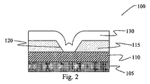
図2は、製造の中間状態における活物質素子100を描いている。素子は、基板105上に形成された下部電極110を含んでいる。基板105は、典型的にはシリコンウェーハであり、トランジスター、ダイオード、nドープ領域、pドープ領域又は他の回路又は素子にアクセス又は走査するのに必要な成分を含んでいる。下部電極110は、伝導層であり、典型的には、金属、合金、金属化合物、又は炭素である。代表的な下部電極材料は、Ti、TiN、TiAlN、TiSiN、TiW、C、W、Mo、MoN、TaNを含んでいる。絶縁層115は、下部電極110上に形成される。絶縁層115は、最も普通には、酸化物(例SiO2)又は窒化物(例Si3N4)であり、開口を含む。図2に示された実施形態においては、
絶縁層115の開口は、傾斜した側壁120である。他の実施形態では、側壁は、実質的に垂直である。開口は、下部電極と活物質130の接続領域を確立する。素子をプログラムするのに要するエネルギーを最小にするため、接続領域を最小にすることが望ましい。開口は、リソグラフィーの寸法を確保するため、標準的なリソグラフィー技術(例 マスキングとエッチング)によって形成される。開口は、孔、溝、又はくぼみの形状である。任意的に、この分野で知られているように、側壁スペーサを開口内に含めることにより(図2には示されていない)、サブリソグラフィーによる寸法を確保することができる。
FIG. 2 depicts the
The opening of the insulating
活物質130は、絶縁層115上であって絶縁層115の開口内に形成される。カルコゲニド材料、相変化物質のような活物質は、しばしばスパッタリング又は他の(形状が)一様でない(non−conformal)処理によって形成される。この一様でない処理において、活物質130は、絶縁層115の開口を密に満たすことはない。その代わり、開口は、活物質130によって不完全に満たされる。それに加えて、活物質は、絶縁層115との接続の表面に平行になることはない。図2に示されるように、活物質130の上部表面の形状は、絶縁層115の開口の形状から逸脱している。開口は、線形に傾斜した側壁120と平坦な底部を含むが、活物質130は、開口の近くの湾曲した上部表面と開口の中心に向う一様でない充填物を有する。これらの効果は、一様でない堆積技術が活物質130を形成するのに使用される場合、開口の寸法が減少するにつれてより顕著になる。
The
図2には示されていないが、任意の障壁層が絶縁体115の上で下部電極110と活物質130の間に形成される。この技術分野で知られているように、障壁層は、典型的には、原子成分が活物質130と下部電極110の間を(拡散又はエレクトロマイグレーションによって)行ったり来たり移動することを妨げるように働く薄い層である。障壁層の代わりに、又は障壁層に加えて、ブレークダウン層(図2には示されていない)も活物質130と下部電極110の間に形成されることがある。この技術分野で知られているように、ブレークダウン層は、下部電極110と活物質130との間の接続の有効領域を減少させるように使用される薄い絶縁層である。素子の調整の間、電気信号は、ブレークダウン層に穴を開け、下部電極110から活物質130への伝導経路の局在した、小領域の伝導経路を生成する。ブレークダウン層の残りはそのまま変化せず、下部電極から穴が開いた伝導領域への電流の流れをチャネルで導く抵抗障壁を提供する。
Although not shown in FIG. 2, an optional barrier layer is formed on the
図2に示す製造の段階では、電子素子100は不完全であり、製造を完了するためにはさらに堆積ステップと処理ステップが必要である。製造のこの時点において、活性層130は、処理環境に暴露され、後続する製造ステップからの熱劣化(揮発)、化学劣化、化学汚染の作用を受ける。典型的な製造スキームにおいて、上部電極140は、活物質130上に形成される。(図3を参照)化学気相堆積法(CVD)又は金属有機化学気相堆積法(MOCVDのような堆積技術は、(形状が)一様な(conformal)堆積を提供するため、上部電極140の形成に望ましいが、普通の上部電極材料のために現在入手できる前駆物質に基づくと、高い堆積温度(例えば350℃以上)を要するという欠点を有する。上部電極140が高温の堆積処理で形成される場合、堆積環境における高い周囲の温度により活性層130の揮発を引き起こし、活性層130の組成又は構造の完全性を低下させることになる。
In the manufacturing stage shown in FIG. 2, the
活性層130の揮発を低減するため、スパッタリングのような低温堆積処理が上部電極140を提供するために使用される。しかしながら、スパッタリングは、活性層の一様でない被覆を提供するという欠点を有する。スパッタリングを施されたフィルムは、ターゲットの材料からの原子断片又は分子断片の集合体である。ターゲットの材料の断片は、スパッタリング処理においてターゲットのエネルギー衝撃によって放出され、運動エネルギーによって堆積面に運ばれる。断片は堆積面に無秩序に堆積し、ターゲットの材料の組成に近い組成を有する材料の多孔質層を提供する。蒸着のような他の一様でない技術は、同様に構造的に一様でないか濃密でない被覆を堆積面の被覆に提供する。
In order to reduce volatilization of the
多孔質の上部電極層140の不利な点は、以下の処理で顕著になる。ひとたび上部電極140が形成されると、さらに、いくつかのスキームに従って電子装置100の製造が進められる。一つのスキームにおいては、素子は活性層130及び/又は上部電極140を高密度化(焼結)するためにアニールされる。活性層130と上部電極140の一様でない堆積から帰着する多孔質構造は、動作の観点から望ましくないが、これは、構造におけるギャップ又は孔部が電気的性能の信頼性と再現性に影響するからである。例えば電流に付随するジュール熱は、繰り返しの動作回数によって多孔質構造を変化させ、活性層130又は上部電極140の抵抗を変化させることになる。抵抗の変化によって、素子をプログラムするか又は読み出すのに必要とされるパルスの特性が変化する。活性層130と上部電極140との間を接続する物理的領域が動作回数の経過とともに減少する場合、ギャップ又は孔部又は空隙(及び動作回数によるミグレーション)の存在により、開放回路故障が容易に引き起こされるようになる。
The disadvantages of the porous
多孔質構造の欠点を避けるため、活性層130と上部電極140には、高温アニーリングが作用され、構造を強固にし、より一様で高密度な層を提供する。構造を効果的にアニーリングするため、300〜450℃の温度が5〜60分にわたって必要とされる。しかしながら、アニーリングの間、活性層130は、顕著な揮発を招くような高温に暴露される。上部電極140が多孔質構造である場合、開発した活性層材料が脱出する孔部を含む。上述したように、一般に、活性層130の揮発は、異なる原子成分の相対的な揮発度の相違によって、活性層130の揮発していない部分の組成が意図した組成からの変化することを招来する。また、活性層材料の体積損失は、アニーリング処理で望まれる強固にすることとは逆に働き、電気的性能を低下させる空隙を生じる。
In order to avoid the disadvantages of the porous structure, high temperature annealing is applied to the
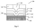
また、高温の処理環境は、アニーリングとは他のステップにも存在する。例えば、アレイ構造においては、上部電極140から外部アドレス線に接続することが必要となる。接続の一つの方法は、上部電極140上に垂直伝導プラグを形成することである。図4は、代表的なプラグ構造を概略的に示している。素子は、プラグ150で満たされる開口を含む絶縁層145を含み、プラグ150は、活性層130と周囲との間の電気的な接続を提供する。最も普通のプラグ材料であるタングステンは、堆積に300℃をはるかに上回る温度が必要であり、揮発が生じるような条件に活性層130を長時間にわたって暴露することになる。上部電極140が多孔質の場合、活性層130からの揮発性物質が脱出し、上述のように、活性相の組成と構造の完全性が低下することになる。
Also, a high temperature processing environment exists in other steps than annealing. For example, in the array structure, it is necessary to connect the
他の普通の高温処理ステップは、上部電極140に続く絶縁層の形成である。絶縁層は、完成した素子を空気、蒸気又は他の外部汚染、さらには機械的衝撃又は擦過傷から保護するために上部電極140上に形成される。また、絶縁層は、隣接する素子を電気的に分離するため、アレイ構造に組み込まれる。素子は、フォトレジストを構造上に堆積し、個々の素子をマスキングし、マスクされていないフォトレジストを除去し、下にあるマスクされていない層をエッチングし、さらに開口領域に絶縁体を堆積することによって分離される。図5は、分離された素子の構造の例を示している。構造は、絶縁層150を含み、活性層130と上部電極140のアレイにおける隣接素子からの電気的分離を提供する。
Another common high temperature processing step is the formation of an insulating layer following the
絶縁層150は、典型的には、酸化物(例SiO2)又は窒化物(Si3N4)であり、比較的高温のHDP(高密度プラズマ)堆積処理、プラズマ化学気相堆積(PECVD)処理、又は化学気相堆積(CVD)処理によって形成される。活性層130の揮発に関する懸念に加え、酸化物と窒化物堆積処理には、活性層130の汚染の懸念がある。酸化物又は窒化物絶縁体の形成には、堆積環境に前駆ガスを導入する必要がある。N2、O2、NO、NOX、N2O、SiH4、SiH2Cl2、H2は、酸化物絶縁体と窒化物絶縁体の形成に普通に使用される。前記形成の処理の間、前駆物質は、絶縁層150を生成するために反応又は分解する。前記形成の処理の間、活物質130は、前駆ガス(及び反応生成物と分解生成物)に暴露される。上部電極140が一様でない及び/又は多孔質である場合、前駆ガスはそれに浸透し、上部電極140に存在する空孔又はチャネルに入る。これによって、N、O、Si、H、Clのような元素によって活性層130の化学汚染が発生する恐れがある。
Insulating
本発明では、上述した従来の製造スキームにおける高温ステップについて有害な揮発と汚染の効果を素子構造に閉じ込め層を設けることによって改善している。図6は、閉じ込め層160を含む代表的な装置構造100を描いている。閉じ込め層160は、この実施の形態では上部電極140上に形成される。閉じ込め層160は、厳密に一様である必要はないが、上部電極140に存在する孔部又は空隙へのアクセスを阻止するために十分に一様であり、十分に厚くなければならない。また、閉じ込め層堆積は、十分に低温で、活物質130の揮発温度より十分に低い温度でなければならない。閉じ込め層160は、準一様層と称される。閉じ込め層160は、上部電極140の上面に浸透するが、活材料層130を周囲処理環境から分離する物理的障壁を提供するため、上部電極140上又は上側に位置する。閉じ込め層160は、上部電極150の上面においてその多孔質ネットワークへの入口をふさいでいる。また、閉じ込め層160は、開口の周囲を密封する材料に連続する被覆を提供することによって、上部電極140の上面開口を遮蔽している。
In the present invention, the detrimental volatilization and contamination effects of high temperature steps in the conventional manufacturing scheme described above are improved by providing a confinement layer in the device structure. FIG. 6 depicts an
上部電極140の空隙構造へのアクセスを制限し、又は完全に阻んでいるため、この閉じ込め層は、二つの顕著な利点を有している。第一に、閉じ込め層160は、製造中に処理環境において周囲のガスへの活物質層130の暴露を阻止する。閉じ込め層160が所定位置にある場合、周囲の処理間極におけるガスは、上部電極の多孔質構造に入ることができず、活物質層130にミグレートすることが防止される。この結果、化学汚染又は周囲の処理ガスと活物質層130との反応が回避される。第二に、閉じ込め層160は、活物質層130を包含し、その揮発を防止する。製造の間、閉じ込め層160が所定位置にあり、構造に高温が作用している場合、閉じ込め層160は、活物質130からの物質の脱出を防止する。この結果、構造は、活物質130の組成又は構造の完全性を低下させることなく、アニーリングステップと高温の堆積ステップに暴露することができる。
This confinement layer has two significant advantages because it restricts or completely prevents access to the void structure of the
素子の製造後、後続する素子の処理の間又は動作の間、閉じ込め層160の存在は、活物質130の環境からの外部汚染(例、大気からの酸素又は水蒸気)を防ぎ、活性層130からの揮発した物質の脱出を防ぐ。上述したように、相変化物質をアモルファス相又はより多くのアモルファス相にプログラミングするには、融解温度を超える温度に材料を加熱する必要がある。また、上述のように、相変化物質を結晶相又はより多くの結晶相にプログラミングするには、迅速な結晶化を促進するために十分な温度に材料を加熱する必要がある。加熱状態又は融解状態にあると、相変化物質は揮発する。閉じ込め層160の存在は、活物質130の局所的な環境は密封し、材料の損失を保護するとともに、活性層の完全性を維持する。
After device fabrication, during the subsequent device processing or operation, the presence of the
好ましい実施形態においては、閉じ込め層160は、活物質130が汚染する潜在性のある化学種を含む高温の処理ステップ又は処理環境に暴露される前に、低温の処理を通じて形成される。この実施形態においては、電子素子100の製造は、図2に示す中間段階に進む。活材料130は、スパッタリング、物理気相堆積、化学気相堆積、金属有機気相堆積、プラズマ気相堆積、溶液相堆積、選択堆積、原子層堆積、蒸着又は他の手段を通じて堆積される。活物質130は、相変化物質、カルコゲニド材料、ニクティド材料、Ovonic閾値スイッチ材料又は他の電子材料である。活物質130は、複数の層を含む。一つの実施形態においては、活物質130は、異なる化学組成を有するカルコゲニド材料又は相変化物質を含む多層構造である。
In a preferred embodiment, the
ひとたび活材料130が堆積すると、活物質を揮発するのには不足すると思われる温度において実施される処理を用いることで、その上に一つ以上の追加の層を形成することができる。一つ以上の追加の層は、障壁層、ブレークダウン層及び/又は上部電極層を含む。上部電極層は、伝導材料から形成され、組成又は抵抗の異なる二つ以上の伝導層の組み合わせを含む。図3は、単一の上部電極層140が活物質130上に堆積した実施形態を描いている。一つ以上の追加の層は、スパッタリング、物理気相堆積、化学気相堆積、金属有機気相堆積、プラズマ気相堆積、溶液相堆積、選択堆積、原子層堆積、蒸着又は他の手段を通じて堆積される。一つの実施形態においては、一つ以上の追加の層のそれぞれの堆積の温度は、活物質130の揮発温度の80%以下である。他の実施形態においては、一つ以上の追加の層のそれぞれの堆積の温度は、活物質130の揮発温度の65%以下である。さらなる実施形態においては、一つ以上の追加の層のそれぞれの堆積の温度は、活物質130の揮発温度の50%以下である。さらに他の実施形態においては、一つ以上の追加の層のそれぞれの堆積の温度は、300℃より低い。
Once the
一つ以上の追加の最後の層が堆積した後、素子は、閉じ込め層が形成される後まで、好ましくは高い周囲の温度から保護される。また、閉じ込め層160は、低温で、スパッタリング、物理気相堆積、化学気相堆積、金属有機気相堆積、プラズマ気相堆積、溶液相堆積、選択堆積、原子層堆積、蒸着又は他の手段を通じて堆積される。一つの実施形態において、閉じ込め層160の堆積の温度は、活物質130の揮発温度の80%以下である。他の実施形態において、閉じ込め層160の堆積の温度は、活物質130の揮発温度の65%以下である。さらなる実施形態において、閉じ込め層160の堆積の温度は、活物質130の揮発温度の50%以下である。さらに他の実施形態において、閉じ込め層160の堆積の温度は、300℃より低い。例として、閉じ込め層160は、プラズマ気相堆積処理により250℃で堆積した酸化物(例SiO2)又は窒化物(例Si3N4)である。他の例においては、閉じ込め層160は、エネルギービーム処理(ターゲットの金属にエネルギーを有する電子ビーム又はイオンビームを当て、後続して電子素子に堆積する金属の元素断片またな分子断片を放出するようにする)又は蒸着処理において形成される。
After the deposition of one or more additional final layers, the device is preferably protected from high ambient temperatures until after the confinement layer is formed. Also, the
図2〜6(多孔質セル構造)に示されるような開口において形成された活物質130の構造の追加において、本発明の原則は、他の素子構造まで拡張される。この閉じ込め層の好ましい密封の効果は、ランスセル(lance cell:槍型セル)構造、埋め込み式のランスセル(recessed lance cell:埋め込み式槍型セル)構造、マイクロトレンチ(microtrench:超小型溝)構造、さらに素子アレイに拡張される。
In addition to the structure of the
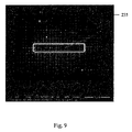
この実施例においては、多孔質セルを有する電子素子が対比され、閉じ込め層を含むことにより素子の動作回数寿命の顕著な延長が提供されることが明示される。この例で使用される素子の断面顕微鏡像が図7に示されている。素子200は、酸化物表面層、TiAlN下部電極201(約650Å厚)、絶縁体215(約375Å厚)、カルコゲニド相変化物質(Ge2Sb2Te5)(約750Å厚)を有する活性層220、Ti/TiN上部電極225(約20ÅのTiであり、活性層220と上の約600ÅのTiNと接続する)。基板205、下部電極210、絶縁体215ベースとなるウエハーを形成し、その上に、低温のスパッタリング処理を用いて活性層220と上部電極225が堆積された。電子素子200は、図3に示したものと同様の多孔質セル構造を有している。活性層220は、絶縁体215の開口を占め(図7の中央近く)、上部電極225は開口の上に位置する活性層220のくぼみを占める。絶縁体215における開口の径は、約1250Åである。図7に示す顕微鏡像は、プログラミングが行われる前の製造したままの状態を描いている。図7は、活性層220が絶縁層215の開口を満たすことを示している。開口内の活性層220においては、空隙は検出されなかった。
In this embodiment, it is demonstrated that an electronic device having a porous cell is contrasted and that the inclusion of a confinement layer provides a significant extension of the device's operating lifetime. A cross-sectional microscopic image of the element used in this example is shown in FIG. The
図7に示す種類の複数の素子が組み立てられ、動作回数寿命にわたってテストされた。二つの一連の動作寿命テストが実施された。一つの一連の組では、図7に示す構造を有する素子がテストされた。他の一連の組では、閉じ込め層が上部電極225上に堆積されたので、構造は図7に示すものとは異なるものになった。図8は、閉じ込め層を欠く一連の組からの素子の上面図を示す。図8の注目すべき特徴は、絶縁体215の開口層上に位置するくぼみ230の存在である。くぼみ230は、処理又は動作の間に高温に加熱されているとき、活性層220を処理の周囲環境に暴露し、活性層220からの揮発物質の脱出を許容する、構造的な不整形状を表している。図9は、矩形状の閉じ込め層235(境界が白線でハイライトされている)を含む一連の組からの素子の対応する上面図を示している。閉じ込め層235は、電子ビーム処理によって作成されたPtの準一様層である。閉じ込め層235は、絶縁層215の開口上に直接に形成され、活性層220を有効に密封する。周囲のガスは、活性層220にアクセスすることはできず、活性層220から揮発した物質は、脱出することはできない。
Multiple elements of the type shown in FIG. 7 were assembled and tested over the operational lifetime. Two series of operational life tests were conducted. In one series, devices having the structure shown in FIG. 7 were tested. In another series, the structure was different from that shown in FIG. 7 because the confinement layer was deposited on
閉じ込め層235の有無に応じた素子の動作回数寿命がテストされ対比された。この動作回数寿命のテストにおいて、素子は、セット状態とリセット状態との間を繰返し行ったり来たりする動作を繰り返された。動作の各回数におけるセット状態とリセット状態の抵抗が測定され記録された。テストは、素子に故障が生じるまで継続された。閉じ込め層を有しない代表的な素子の動作回数テストの動作回数寿命の結果は、図10の上部の二つの軌跡に示されている(図10の下部の三つの軌跡は、この検討の対象ではない素子の他の動作パラメータであるVt(閾値電圧)、Vh(保持電圧)、dV/dI(I−V応答曲線の傾斜)を示している)。最上部の軌跡は、素子のリセット抵抗(約106Ω)を示し、最上部の次の軌跡は、素子のセット抵抗(約104Ω)を示す。素子の故障は、セット状態の軌跡の端から出ている急勾配の線によって示されている。この結果は、素子は約4×107動作回数の後で故障することを示している。
The lifetime of operation of the device depending on the presence or absence of the
Pt閉じ込め層を含む代表的な素子についての同様な結果が図11に示されている。図11の上部の二つの軌跡は、素子のリセット抵抗(約106Ω)を示し、最上部から次の軌跡は、素子のセット抵抗(約104Ω)を示す。閉じ込め層の存在によって、素子の動作回数寿命は大きく延びる。素子は、故障する前に約1010もの動作回数を実行した。この結果は、故障の態様が、「停止セット(stuck set)」故障に変化したことを示している。 Similar results for a representative device including a Pt confinement layer are shown in FIG. The two traces in the upper part of FIG. 11 indicate the reset resistance (about 10 6 Ω) of the element, and the next trace from the top indicates the set resistance (about 10 4 Ω) of the element. Due to the presence of the confinement layer, the device operating life is greatly extended. The device performed as many as about 10 10 operations before failing. This result indicates that the failure mode has changed to a “stuck set” failure.
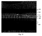
図12は、故障後の閉じ込め層を欠く素子の断面顕微鏡像を示している。顕微鏡像において注目すべきものは、空隙240の存在である。空隙240は、絶縁体215の開口内の脱出領域を表し、素子の故障は活性層220の揮発によることを示唆している。閉じ込め層を欠くことにより、活性層220の揮発と素子の動作部分からの物質の損失が許されるようになる。上述のように、相変化素子をリセット状態にプログラミングするには、相変化物質を融解させるのに十分な強度の電流パルスを印加することが必要である。同じく上述のように、相変化素子をセット状態にプログラミングするには、相変化物質を結晶化させるのに十分な強度の電流パルスを印加することが必要である。融解状態又は結晶化の間、相変化物質は揮発性であり、揮発した部分は、図8に示したくぼみ230を通じて構造を出ることで脱出することができる。また、くぼみ230の存在により、動作を繰り返す過程において環境の酸素が活性層220にアクセスすることが許容される。融解した高温状態又は結晶化している高温状態において、活性層220の近くに酸素が存在することにより、酸化又は他の化学反応によって活性層220の劣化が容易に引き起こされるようになる。活性層220の揮発及び/又は反応は、素子を早期の故障に導くことが予想され、素子で観察される低い動作回数寿命の原因になると想定される。
FIG. 12 shows a cross-sectional microscopic image of the device lacking the confinement layer after failure. What should be noted in the microscopic image is the presence of the
図13は、故障後の閉じ込め層235を含む素子の対応する顕微鏡像を示す。この顕微鏡像は、絶縁体215の開口内には空隙が存在しないことを示している。これに代わって、結晶性凝集体245が観察された。理論によって束縛することは望まないが、本発明者は、素子の故障は、素子の繰返しの動作回数によるGe2Sb2Te5の結晶性凝集体245の非可逆的な形成によるものであると推測している。結晶相は、絶縁体215の開口を迂回した上部電極225への伝導経路を提供する低抵抗相である。結晶性凝集体245は、下部電極210と活性層210の周辺部分(絶縁体215の開口から離れた部分)との間のギャップをまたいでいるようである。周辺部分は、活性層220のアモルファス相よりもより伝導性であると予測されるので、結晶性凝集体245が動作回数を経てアモルファス相に変換されることが不可能になると、結晶性凝集体245の存在によって、下部電極210と上部電極225との間の永続的な低抵抗の経路がもたらされる。
FIG. 13 shows a corresponding microscopic image of the device including the
この実施例の結果は、相変化物質の構造において閉じ込め層を含むことによる有益な効果を明示するものである。素子の動作回数寿命は、閉じ込め層を含むことによって二の次数の強度だけ増加することが観測された。閉じ込め層の存在により、活性層220の揮発又は酸化による早期の故障が防がれ、結晶性凝集体の非可逆の形成と偏在による故障の新たな態様が示唆された。動作回数をさらに延ばす将来の研究の新たな方向も示された。
The results of this example demonstrate the beneficial effect of including a confinement layer in the structure of the phase change material. It was observed that the operating lifetime of the device increased by a second order intensity by including a confinement layer. The presence of the confinement layer prevented early failure due to volatilization or oxidation of the
本発明は、特に前述の実施形態を参照して、示され、記載されたが、これらは、この発明を実施するための裁量の形態を説明するためのものに過ぎない。当業者には、ここで記載した発明の実施形態のさまざまな他の態様が、特許請求の範囲に出規定した発明の趣旨と範囲から逸脱することなく、この発明を実施するに当たって適用できるであろう。実施形態は、記載した成分の全ての新規で自明でない組み合わせを含むと理解され、特許請求の範囲は、これらの成分のいずれかの新規な自明でない組み合わせを対象とするこの出願又は後の出願において提示される。さらに、前述の実施形態は、説明のためであり、いずれの単一の特徴又は成分もこの出願又は後の出願において特許請求の範囲となる全ての可能な組み合わせに対して必須ではない。 Although the invention has been shown and described, particularly with reference to the foregoing embodiments, these are merely illustrative of the discretionary form for carrying out the invention. It will be apparent to those skilled in the art that various other aspects of the embodiments of the invention described herein can be applied in practicing the invention without departing from the spirit and scope of the invention as defined in the claims. Let's go. Embodiments are understood to include all novel and non-obvious combinations of the components described, and the claims are intended in this or a later application directed to any novel non-obvious combination of these components. Presented. Furthermore, the foregoing embodiments are illustrative, and no single feature or ingredient is required for every possible combination that is claimed in this or a later application.
記載したプロセス、方法、ヒューリスティクス等について、このようなプロセス等は、所定の順序の流れに従って起こるように記載したが、このようなプロセスは、記載されたステップによって、記載した順序とは異なる順序で実施されることができると理解される。さらに、所定のステップが同時に実行され、他のステップが追加され、記載した所定のステップは省略されることができると理解される。記載したプロセスの記載は、所定の実施形態を説明するために提供されたものであって、特許請求の範囲に係る発明の限界を規定するものではない。 For the processes, methods, heuristics, etc. described, such processes, etc. have been described to occur according to a predetermined sequence flow, but such processes may differ from the described order by the steps described. It is understood that can be implemented with. Further, it will be understood that certain steps may be performed simultaneously, other steps may be added, and certain steps described may be omitted. The described process descriptions are provided to illustrate certain embodiments and do not define the limits of the claimed invention.
したがって、上述の記載は、説明のためであり、限定するものではない。提供された実施例のほかの多くの実施形態と応用が、当業者には上述の記載を読むことによって容易である。この発明の範囲は、上述の記載によって規定されるのではなく、添付の特許請求の範囲によって、このような特許請求の範囲に権利を与えられるその同等物の全範囲とともに規定される。検討した技術分野における将来的な発展が予想または意図され、開示されたシステムと方法は、そのような将来の実施形態に組み込まれる。つまり、この発明は、変更と修正が可能であり、以下の特許請求の範囲によってのみ限定される。 Accordingly, the foregoing description is by way of illustration and not limitation. Many other embodiments and applications of the examples provided will be readily apparent to those skilled in the art upon reading the foregoing description. The scope of the invention is not defined by the above description, but by the appended claims, along with the full scope of equivalents to which such claims are entitled. Future developments in the considered technical field are anticipated or intended, and the disclosed systems and methods are incorporated into such future embodiments. That is, the present invention can be changed and modified and is limited only by the following claims.
特許請求の範囲の全ての用語は、明示の注意がない限り、最も合理で広い解釈で当業者によって解される通常の意味であるように意図されている。特に、「ある」、「その」、「前記」等のような単数の冠詞は、明示の注意がない限り、一以上の構成要素を意図するものである。 All terms in the claims are intended to have their ordinary meanings as understood by one of ordinary skill in the most reasonable and broadest interpretation, unless expressly noted. In particular, singular articles such as “a”, “the”, “above” and the like are intended to be one or more components, unless expressly noted.
Claims (40)
第1の電極と、
前記第1の電極上に形成された活物質と、
前記活物質上に一様でないように形成され、孔部を含み、前記孔部は前記活物質を前記素子の周囲の環境に暴露する、第2の電極と、
前記第2の電極上に形成され、前記孔部を被覆し、前記活物質を前記素子の前記周囲の環境から密封する閉じ込め層と
を有する素子。 In electronic devices,
A first electrode;
An active material formed on the first electrode;
A second electrode formed non-uniformly on the active material, including a hole, the hole exposing the active material to an environment surrounding the device;
A device having a confinement layer formed on the second electrode, covering the hole, and sealing the active material from the surrounding environment of the device.
基板を提供するステップと、
前記基板上に第1の電極を形成するステップと、
前記第1の基板上に活物質を形成し、前記活物質は、揮発温度を有するステップと、
前記活物質の前記揮発温度以下の温度において、前記活物質上に第2の電極を形成するステップと
を有する方法。 In a method of manufacturing an electronic device,
Providing a substrate;
Forming a first electrode on the substrate;
Forming an active material on the first substrate, the active material having a volatilization temperature;
Forming a second electrode on the active material at a temperature equal to or lower than the volatilization temperature of the active material.
Applications Claiming Priority (2)
| Application Number | Priority Date | Filing Date | Title |
|---|---|---|---|
| US11/999,158 US7718990B2 (en) | 2007-12-04 | 2007-12-04 | Active material devices with containment layer |
| PCT/US2008/013330 WO2009073188A2 (en) | 2007-12-04 | 2008-12-04 | Active material devices with containment layer |
Publications (2)
| Publication Number | Publication Date |
|---|---|
| JP2011505708A true JP2011505708A (en) | 2011-02-24 |
| JP2011505708A5 JP2011505708A5 (en) | 2011-09-29 |
Family
ID=40674790
Family Applications (1)
| Application Number | Title | Priority Date | Filing Date |
|---|---|---|---|
| JP2010536925A Pending JP2011505708A (en) | 2007-12-04 | 2008-12-04 | Active material device having confinement layer |
Country Status (5)
| Country | Link |
|---|---|
| US (2) | US7718990B2 (en) |
| JP (1) | JP2011505708A (en) |
| KR (1) | KR101006218B1 (en) |
| TW (1) | TWI470847B (en) |
| WO (1) | WO2009073188A2 (en) |
Cited By (2)
| Publication number | Priority date | Publication date | Assignee | Title |
|---|---|---|---|---|
| JP2013013081A (en) * | 2011-06-27 | 2013-01-17 | Commissariat A L'energie Atomique Et Aux Energies Alternatives | Delay generator using programmable resistor based on phase-change material |
| KR101573015B1 (en) * | 2015-01-09 | 2015-11-30 | 연세대학교 산학협력단 | Phase chang materials declining activation energy, phase-change memory resistive elements comprising the same and preparation method thereof |
Families Citing this family (67)
| Publication number | Priority date | Publication date | Assignee | Title |
|---|---|---|---|---|
| US7778063B2 (en) * | 2006-11-08 | 2010-08-17 | Symetrix Corporation | Non-volatile resistance switching memories and methods of making same |
| US20090180313A1 (en) * | 2008-01-15 | 2009-07-16 | Wim Deweerd | Chalcogenide anti-fuse |
| US20100225989A1 (en) * | 2009-03-05 | 2010-09-09 | The Regents Of The University Of California | Phase change device |
| JP2013522912A (en) * | 2010-03-16 | 2013-06-13 | サンディスク スリーディー,エルエルシー | Bottom electrode for use with metal oxide resistivity switching layers |
| US9601692B1 (en) | 2010-07-13 | 2017-03-21 | Crossbar, Inc. | Hetero-switching layer in a RRAM device and method |
| US8946046B1 (en) | 2012-05-02 | 2015-02-03 | Crossbar, Inc. | Guided path for forming a conductive filament in RRAM |
| US9012307B2 (en) | 2010-07-13 | 2015-04-21 | Crossbar, Inc. | Two terminal resistive switching device structure and method of fabricating |
| US9570678B1 (en) | 2010-06-08 | 2017-02-14 | Crossbar, Inc. | Resistive RAM with preferental filament formation region and methods |
| WO2011156787A2 (en) | 2010-06-11 | 2011-12-15 | Crossbar, Inc. | Pillar structure for memory device and method |
| US8367460B2 (en) * | 2010-06-22 | 2013-02-05 | Micron Technology, Inc. | Horizontally oriented and vertically stacked memory cells |
| US8374018B2 (en) | 2010-07-09 | 2013-02-12 | Crossbar, Inc. | Resistive memory using SiGe material |
| US8884261B2 (en) | 2010-08-23 | 2014-11-11 | Crossbar, Inc. | Device switching using layered device structure |
| US8467227B1 (en) | 2010-11-04 | 2013-06-18 | Crossbar, Inc. | Hetero resistive switching material layer in RRAM device and method |
| US8947908B2 (en) | 2010-11-04 | 2015-02-03 | Crossbar, Inc. | Hetero-switching layer in a RRAM device and method |
| US8168506B2 (en) | 2010-07-13 | 2012-05-01 | Crossbar, Inc. | On/off ratio for non-volatile memory device and method |
| US8569172B1 (en) | 2012-08-14 | 2013-10-29 | Crossbar, Inc. | Noble metal/non-noble metal electrode for RRAM applications |
| US8889521B1 (en) | 2012-09-14 | 2014-11-18 | Crossbar, Inc. | Method for silver deposition for a non-volatile memory device |
| US8492195B2 (en) | 2010-08-23 | 2013-07-23 | Crossbar, Inc. | Method for forming stackable non-volatile resistive switching memory devices |
| US9401475B1 (en) | 2010-08-23 | 2016-07-26 | Crossbar, Inc. | Method for silver deposition for a non-volatile memory device |
| US8404553B2 (en) | 2010-08-23 | 2013-03-26 | Crossbar, Inc. | Disturb-resistant non-volatile memory device and method |
| US8558212B2 (en) | 2010-09-29 | 2013-10-15 | Crossbar, Inc. | Conductive path in switching material in a resistive random access memory device and control |
| US8391049B2 (en) | 2010-09-29 | 2013-03-05 | Crossbar, Inc. | Resistor structure for a non-volatile memory device and method |
| US8389971B2 (en) | 2010-10-14 | 2013-03-05 | Sandisk 3D Llc | Memory cells having storage elements that share material layers with steering elements and methods of forming the same |
| US8841648B2 (en) | 2010-10-14 | 2014-09-23 | Sandisk 3D Llc | Multi-level memory arrays with memory cells that employ bipolar storage elements and methods of forming the same |
| US8502185B2 (en) | 2011-05-31 | 2013-08-06 | Crossbar, Inc. | Switching device having a non-linear element |
| USRE46335E1 (en) | 2010-11-04 | 2017-03-07 | Crossbar, Inc. | Switching device having a non-linear element |
| US8930174B2 (en) | 2010-12-28 | 2015-01-06 | Crossbar, Inc. | Modeling technique for resistive random access memory (RRAM) cells |
| US8815696B1 (en) | 2010-12-31 | 2014-08-26 | Crossbar, Inc. | Disturb-resistant non-volatile memory device using via-fill and etchback technique |
| US9153623B1 (en) | 2010-12-31 | 2015-10-06 | Crossbar, Inc. | Thin film transistor steering element for a non-volatile memory device |
| US8791010B1 (en) | 2010-12-31 | 2014-07-29 | Crossbar, Inc. | Silver interconnects for stacked non-volatile memory device and method |
| WO2012103551A1 (en) * | 2011-01-28 | 2012-08-02 | Greentech Solutions, Inc. | Heating layers containing volatile components at elevated temperatures |
| KR101724084B1 (en) * | 2011-03-03 | 2017-04-07 | 삼성전자 주식회사 | Methods of fabricating a semiconductor device |
| US9620206B2 (en) | 2011-05-31 | 2017-04-11 | Crossbar, Inc. | Memory array architecture with two-terminal memory cells |
| US8619459B1 (en) | 2011-06-23 | 2013-12-31 | Crossbar, Inc. | High operating speed resistive random access memory |
| US8946669B1 (en) | 2012-04-05 | 2015-02-03 | Crossbar, Inc. | Resistive memory device and fabrication methods |
| US9166163B2 (en) | 2011-06-30 | 2015-10-20 | Crossbar, Inc. | Sub-oxide interface layer for two-terminal memory |
| US9627443B2 (en) | 2011-06-30 | 2017-04-18 | Crossbar, Inc. | Three-dimensional oblique two-terminal memory with enhanced electric field |
| US9564587B1 (en) | 2011-06-30 | 2017-02-07 | Crossbar, Inc. | Three-dimensional two-terminal memory with enhanced electric field and segmented interconnects |
| US8659929B2 (en) | 2011-06-30 | 2014-02-25 | Crossbar, Inc. | Amorphous silicon RRAM with non-linear device and operation |
| US9252191B2 (en) | 2011-07-22 | 2016-02-02 | Crossbar, Inc. | Seed layer for a p+ silicon germanium material for a non-volatile memory device and method |
| US8674724B2 (en) | 2011-07-29 | 2014-03-18 | Crossbar, Inc. | Field programmable gate array utilizing two-terminal non-volatile memory |
| US10056907B1 (en) | 2011-07-29 | 2018-08-21 | Crossbar, Inc. | Field programmable gate array utilizing two-terminal non-volatile memory |
| US9729155B2 (en) | 2011-07-29 | 2017-08-08 | Crossbar, Inc. | Field programmable gate array utilizing two-terminal non-volatile memory |
| US8716098B1 (en) | 2012-03-09 | 2014-05-06 | Crossbar, Inc. | Selective removal method and structure of silver in resistive switching device for a non-volatile memory device |
| US9087576B1 (en) | 2012-03-29 | 2015-07-21 | Crossbar, Inc. | Low temperature fabrication method for a three-dimensional memory device and structure |
| US9685608B2 (en) | 2012-04-13 | 2017-06-20 | Crossbar, Inc. | Reduced diffusion in metal electrode for two-terminal memory |
| US8658476B1 (en) | 2012-04-20 | 2014-02-25 | Crossbar, Inc. | Low temperature P+ polycrystalline silicon material for non-volatile memory device |
| US8796658B1 (en) | 2012-05-07 | 2014-08-05 | Crossbar, Inc. | Filamentary based non-volatile resistive memory device and method |
| US8765566B2 (en) | 2012-05-10 | 2014-07-01 | Crossbar, Inc. | Line and space architecture for a non-volatile memory device |
| US10096653B2 (en) | 2012-08-14 | 2018-10-09 | Crossbar, Inc. | Monolithically integrated resistive memory using integrated-circuit foundry compatible processes |
| US9583701B1 (en) | 2012-08-14 | 2017-02-28 | Crossbar, Inc. | Methods for fabricating resistive memory device switching material using ion implantation |
| US8946673B1 (en) | 2012-08-24 | 2015-02-03 | Crossbar, Inc. | Resistive switching device structure with improved data retention for non-volatile memory device and method |
| US9312483B2 (en) | 2012-09-24 | 2016-04-12 | Crossbar, Inc. | Electrode structure for a non-volatile memory device and method |
| US9576616B2 (en) | 2012-10-10 | 2017-02-21 | Crossbar, Inc. | Non-volatile memory with overwrite capability and low write amplification |
| US11068620B2 (en) | 2012-11-09 | 2021-07-20 | Crossbar, Inc. | Secure circuit integrated with memory layer |
| US8982647B2 (en) | 2012-11-14 | 2015-03-17 | Crossbar, Inc. | Resistive random access memory equalization and sensing |
| US9412790B1 (en) | 2012-12-04 | 2016-08-09 | Crossbar, Inc. | Scalable RRAM device architecture for a non-volatile memory device and method |
| US9406379B2 (en) | 2013-01-03 | 2016-08-02 | Crossbar, Inc. | Resistive random access memory with non-linear current-voltage relationship |
| US9324942B1 (en) | 2013-01-31 | 2016-04-26 | Crossbar, Inc. | Resistive memory cell with solid state diode |
| US9112145B1 (en) | 2013-01-31 | 2015-08-18 | Crossbar, Inc. | Rectified switching of two-terminal memory via real time filament formation |
| US8934280B1 (en) | 2013-02-06 | 2015-01-13 | Crossbar, Inc. | Capacitive discharge programming for two-terminal memory cells |
| US10290801B2 (en) | 2014-02-07 | 2019-05-14 | Crossbar, Inc. | Scalable silicon based resistive memory device |
| US10424731B2 (en) | 2015-03-13 | 2019-09-24 | Toshiba Memory Corporation | Memory device |
| KR20180107806A (en) * | 2017-03-22 | 2018-10-04 | 삼성전자주식회사 | Method of forming a layer, and method of foriming variable resistance memory devices using the same |
| KR20190007642A (en) * | 2017-07-13 | 2019-01-23 | 에스케이하이닉스 주식회사 | Neuromorphic Device Having a Plurality of Synapse Blocks |
| US10937961B2 (en) | 2018-11-06 | 2021-03-02 | International Business Machines Corporation | Structure and method to form bi-layer composite phase-change-memory cell |
| US11659780B2 (en) | 2019-03-05 | 2023-05-23 | International Business Machines Corporation | Phase change memory structure with efficient heating system |
Citations (5)
| Publication number | Priority date | Publication date | Assignee | Title |
|---|---|---|---|---|
| US6189582B1 (en) * | 1997-05-09 | 2001-02-20 | Micron Technology, Inc. | Small electrode for a chalcogenide switching device and method for fabricating same |
| JP2004158852A (en) * | 2002-11-01 | 2004-06-03 | Samsung Electronics Co Ltd | Phase conversion memory device and its manufacturing method |
| JP2006182781A (en) * | 2004-12-27 | 2006-07-13 | Samsung Electronics Co Ltd | Germanium precursor, gst thin film formed by utilizing the same, method for producing the thin film and phase change memory element |
| JP2006245539A (en) * | 2005-02-03 | 2006-09-14 | Toshiba Corp | Semiconductor memory device |
| JP2006351992A (en) * | 2005-06-20 | 2006-12-28 | Renesas Technology Corp | Semiconductor storage device and manufacturing method thereof |
Family Cites Families (9)
| Publication number | Priority date | Publication date | Assignee | Title |
|---|---|---|---|---|
| US6784018B2 (en) * | 2001-08-29 | 2004-08-31 | Micron Technology, Inc. | Method of forming chalcogenide comprising devices and method of forming a programmable memory cell of memory circuitry |
| US7087919B2 (en) * | 2002-02-20 | 2006-08-08 | Micron Technology, Inc. | Layered resistance variable memory device and method of fabrication |
| WO2004008535A1 (en) * | 2002-07-11 | 2004-01-22 | Matsushita Electric Industrial Co., Ltd. | Nonvolatile memory and its manufacturing method |
| US7402851B2 (en) * | 2003-02-24 | 2008-07-22 | Samsung Electronics Co., Ltd. | Phase changeable memory devices including nitrogen and/or silicon and methods for fabricating the same |
| CN1286716C (en) * | 2003-03-19 | 2006-11-29 | 清华大学 | Method for growing carbon nano tube |
| KR20050053255A (en) * | 2003-12-02 | 2005-06-08 | 삼성전자주식회사 | Phase-changable memory device and method of forming the same |
| CN101834198A (en) * | 2004-05-14 | 2010-09-15 | 瑞萨电子株式会社 | Semiconductor storage unit |
| US7326951B2 (en) * | 2004-12-16 | 2008-02-05 | Macronix International Co., Ltd. | Chalcogenide random access memory |
| US20070045606A1 (en) * | 2005-08-30 | 2007-03-01 | Michele Magistretti | Shaping a phase change layer in a phase change memory cell |
-
2007
- 2007-12-04 US US11/999,158 patent/US7718990B2/en active Active
-
2008
- 2008-12-03 TW TW97146858A patent/TWI470847B/en active
- 2008-12-04 JP JP2010536925A patent/JP2011505708A/en active Pending
- 2008-12-04 WO PCT/US2008/013330 patent/WO2009073188A2/en active Application Filing
- 2008-12-04 KR KR1020107014581A patent/KR101006218B1/en active IP Right Grant
-
2010
- 2010-05-17 US US12/780,966 patent/US7935567B2/en active Active
Patent Citations (5)
| Publication number | Priority date | Publication date | Assignee | Title |
|---|---|---|---|---|
| US6189582B1 (en) * | 1997-05-09 | 2001-02-20 | Micron Technology, Inc. | Small electrode for a chalcogenide switching device and method for fabricating same |
| JP2004158852A (en) * | 2002-11-01 | 2004-06-03 | Samsung Electronics Co Ltd | Phase conversion memory device and its manufacturing method |
| JP2006182781A (en) * | 2004-12-27 | 2006-07-13 | Samsung Electronics Co Ltd | Germanium precursor, gst thin film formed by utilizing the same, method for producing the thin film and phase change memory element |
| JP2006245539A (en) * | 2005-02-03 | 2006-09-14 | Toshiba Corp | Semiconductor memory device |
| JP2006351992A (en) * | 2005-06-20 | 2006-12-28 | Renesas Technology Corp | Semiconductor storage device and manufacturing method thereof |
Cited By (2)
| Publication number | Priority date | Publication date | Assignee | Title |
|---|---|---|---|---|
| JP2013013081A (en) * | 2011-06-27 | 2013-01-17 | Commissariat A L'energie Atomique Et Aux Energies Alternatives | Delay generator using programmable resistor based on phase-change material |
| KR101573015B1 (en) * | 2015-01-09 | 2015-11-30 | 연세대학교 산학협력단 | Phase chang materials declining activation energy, phase-change memory resistive elements comprising the same and preparation method thereof |
Also Published As
| Publication number | Publication date |
|---|---|
| US7718990B2 (en) | 2010-05-18 |
| KR101006218B1 (en) | 2011-01-07 |
| TW200941781A (en) | 2009-10-01 |
| WO2009073188A2 (en) | 2009-06-11 |
| KR20100084196A (en) | 2010-07-23 |
| US20090140229A1 (en) | 2009-06-04 |
| US7935567B2 (en) | 2011-05-03 |
| TWI470847B (en) | 2015-01-21 |
| US20100221868A1 (en) | 2010-09-02 |
| WO2009073188A3 (en) | 2009-08-06 |
Similar Documents
| Publication | Publication Date | Title |
|---|---|---|
| US7935567B2 (en) | Active material devices with containment layer | |
| US7569844B2 (en) | Memory cell sidewall contacting side electrode | |
| US7879645B2 (en) | Fill-in etching free pore device | |
| US7682868B2 (en) | Method for making a keyhole opening during the manufacture of a memory cell | |
| US7749854B2 (en) | Method for making a self-converged memory material element for memory cell | |
| US7696503B2 (en) | Multi-level memory cell having phase change element and asymmetrical thermal boundary | |
| Terao et al. | Electrical phase-change memory: fundamentals and state of the art | |
| US7473576B2 (en) | Method for making a self-converged void and bottom electrode for memory cell | |
| US7507986B2 (en) | Thermal isolation for an active-sidewall phase change memory cell | |
| US7875493B2 (en) | Memory structure with reduced-size memory element between memory material portions | |
| JP6062155B2 (en) | Ge-rich GST-212 phase change material | |
| US8222071B2 (en) | Method for making self aligning pillar memory cell device | |
| US9917252B2 (en) | GaSbGe phase change memory materials | |
| US7956344B2 (en) | Memory cell with memory element contacting ring-shaped upper end of bottom electrode | |
| US20080096344A1 (en) | Method for Manufacturing a Resistor Random Access Memory with a Self-Aligned Air Gap insulator |
Legal Events
| Date | Code | Title | Description |
|---|---|---|---|
| A975 | Report on accelerated examination |
Free format text: JAPANESE INTERMEDIATE CODE: A971005 Effective date: 20101124 |
|
| A131 | Notification of reasons for refusal |
Free format text: JAPANESE INTERMEDIATE CODE: A131 Effective date: 20101207 |
|
| A521 | Request for written amendment filed |
Free format text: JAPANESE INTERMEDIATE CODE: A523 Effective date: 20110307 |
|
| A131 | Notification of reasons for refusal |
Free format text: JAPANESE INTERMEDIATE CODE: A131 Effective date: 20110607 |
|
| A524 | Written submission of copy of amendment under article 19 pct |
Free format text: JAPANESE INTERMEDIATE CODE: A524 Effective date: 20110809 |
|
| A02 | Decision of refusal |
Free format text: JAPANESE INTERMEDIATE CODE: A02 Effective date: 20111115 |
|
| A521 | Request for written amendment filed |
Free format text: JAPANESE INTERMEDIATE CODE: A523 Effective date: 20120224 |
|
| A911 | Transfer to examiner for re-examination before appeal (zenchi) |
Free format text: JAPANESE INTERMEDIATE CODE: A911 Effective date: 20120419 |
|
| A912 | Re-examination (zenchi) completed and case transferred to appeal board |
Free format text: JAPANESE INTERMEDIATE CODE: A912 Effective date: 20120622 |
|
| A601 | Written request for extension of time |
Free format text: JAPANESE INTERMEDIATE CODE: A601 Effective date: 20121029 |
|
| A602 | Written permission of extension of time |
Free format text: JAPANESE INTERMEDIATE CODE: A602 Effective date: 20121101 |