JP2011502352A - Bond pad support structure for semiconductor devices - Google Patents
Bond pad support structure for semiconductor devices Download PDFInfo
- Publication number
- JP2011502352A JP2011502352A JP2010530988A JP2010530988A JP2011502352A JP 2011502352 A JP2011502352 A JP 2011502352A JP 2010530988 A JP2010530988 A JP 2010530988A JP 2010530988 A JP2010530988 A JP 2010530988A JP 2011502352 A JP2011502352 A JP 2011502352A
- Authority
- JP
- Japan
- Prior art keywords
- bond pad
- metallization layer
- metal
- passivation
- passivation structure
- Prior art date
- Legal status (The legal status is an assumption and is not a legal conclusion. Google has not performed a legal analysis and makes no representation as to the accuracy of the status listed.)
- Pending
Links
Images


Classifications
-
- H—ELECTRICITY
- H01—ELECTRIC ELEMENTS
- H01L—SEMICONDUCTOR DEVICES NOT COVERED BY CLASS H10
- H01L24/00—Arrangements for connecting or disconnecting semiconductor or solid-state bodies; Methods or apparatus related thereto
- H01L24/01—Means for bonding being attached to, or being formed on, the surface to be connected, e.g. chip-to-package, die-attach, "first-level" interconnects; Manufacturing methods related thereto
- H01L24/02—Bonding areas ; Manufacturing methods related thereto
- H01L24/04—Structure, shape, material or disposition of the bonding areas prior to the connecting process
- H01L24/05—Structure, shape, material or disposition of the bonding areas prior to the connecting process of an individual bonding area
-
- H—ELECTRICITY
- H01—ELECTRIC ELEMENTS
- H01L—SEMICONDUCTOR DEVICES NOT COVERED BY CLASS H10
- H01L23/00—Details of semiconductor or other solid state devices
- H01L23/52—Arrangements for conducting electric current within the device in operation from one component to another, i.e. interconnections, e.g. wires, lead frames
- H01L23/522—Arrangements for conducting electric current within the device in operation from one component to another, i.e. interconnections, e.g. wires, lead frames including external interconnections consisting of a multilayer structure of conductive and insulating layers inseparably formed on the semiconductor body
- H01L23/528—Geometry or layout of the interconnection structure
-
- H—ELECTRICITY
- H01—ELECTRIC ELEMENTS
- H01L—SEMICONDUCTOR DEVICES NOT COVERED BY CLASS H10
- H01L2224/00—Indexing scheme for arrangements for connecting or disconnecting semiconductor or solid-state bodies and methods related thereto as covered by H01L24/00
- H01L2224/01—Means for bonding being attached to, or being formed on, the surface to be connected, e.g. chip-to-package, die-attach, "first-level" interconnects; Manufacturing methods related thereto
- H01L2224/02—Bonding areas; Manufacturing methods related thereto
- H01L2224/0212—Auxiliary members for bonding areas, e.g. spacers
- H01L2224/02122—Auxiliary members for bonding areas, e.g. spacers being formed on the semiconductor or solid-state body
- H01L2224/02163—Auxiliary members for bonding areas, e.g. spacers being formed on the semiconductor or solid-state body on the bonding area
- H01L2224/02165—Reinforcing structures
- H01L2224/02166—Collar structures
-
- H—ELECTRICITY
- H01—ELECTRIC ELEMENTS
- H01L—SEMICONDUCTOR DEVICES NOT COVERED BY CLASS H10
- H01L2224/00—Indexing scheme for arrangements for connecting or disconnecting semiconductor or solid-state bodies and methods related thereto as covered by H01L24/00
- H01L2224/01—Means for bonding being attached to, or being formed on, the surface to be connected, e.g. chip-to-package, die-attach, "first-level" interconnects; Manufacturing methods related thereto
- H01L2224/02—Bonding areas; Manufacturing methods related thereto
- H01L2224/04—Structure, shape, material or disposition of the bonding areas prior to the connecting process
- H01L2224/05—Structure, shape, material or disposition of the bonding areas prior to the connecting process of an individual bonding area
- H01L2224/05001—Internal layers
- H01L2224/05005—Structure
- H01L2224/05009—Bonding area integrally formed with a via connection of the semiconductor or solid-state body
-
- H—ELECTRICITY
- H01—ELECTRIC ELEMENTS
- H01L—SEMICONDUCTOR DEVICES NOT COVERED BY CLASS H10
- H01L2224/00—Indexing scheme for arrangements for connecting or disconnecting semiconductor or solid-state bodies and methods related thereto as covered by H01L24/00
- H01L2224/01—Means for bonding being attached to, or being formed on, the surface to be connected, e.g. chip-to-package, die-attach, "first-level" interconnects; Manufacturing methods related thereto
- H01L2224/02—Bonding areas; Manufacturing methods related thereto
- H01L2224/04—Structure, shape, material or disposition of the bonding areas prior to the connecting process
- H01L2224/05—Structure, shape, material or disposition of the bonding areas prior to the connecting process of an individual bonding area
- H01L2224/05001—Internal layers
- H01L2224/05075—Plural internal layers
- H01L2224/0508—Plural internal layers being stacked
- H01L2224/05085—Plural internal layers being stacked with additional elements, e.g. vias arrays, interposed between the stacked layers
- H01L2224/05089—Disposition of the additional element
- H01L2224/05093—Disposition of the additional element of a plurality of vias
- H01L2224/05095—Disposition of the additional element of a plurality of vias at the periphery of the internal layers
-
- H—ELECTRICITY
- H01—ELECTRIC ELEMENTS
- H01L—SEMICONDUCTOR DEVICES NOT COVERED BY CLASS H10
- H01L2224/00—Indexing scheme for arrangements for connecting or disconnecting semiconductor or solid-state bodies and methods related thereto as covered by H01L24/00
- H01L2224/01—Means for bonding being attached to, or being formed on, the surface to be connected, e.g. chip-to-package, die-attach, "first-level" interconnects; Manufacturing methods related thereto
- H01L2224/02—Bonding areas; Manufacturing methods related thereto
- H01L2224/04—Structure, shape, material or disposition of the bonding areas prior to the connecting process
- H01L2224/05—Structure, shape, material or disposition of the bonding areas prior to the connecting process of an individual bonding area
- H01L2224/0554—External layer
- H01L2224/0555—Shape
- H01L2224/05556—Shape in side view
- H01L2224/05558—Shape in side view conformal layer on a patterned surface
-
- H—ELECTRICITY
- H01—ELECTRIC ELEMENTS
- H01L—SEMICONDUCTOR DEVICES NOT COVERED BY CLASS H10
- H01L2224/00—Indexing scheme for arrangements for connecting or disconnecting semiconductor or solid-state bodies and methods related thereto as covered by H01L24/00
- H01L2224/01—Means for bonding being attached to, or being formed on, the surface to be connected, e.g. chip-to-package, die-attach, "first-level" interconnects; Manufacturing methods related thereto
- H01L2224/02—Bonding areas; Manufacturing methods related thereto
- H01L2224/04—Structure, shape, material or disposition of the bonding areas prior to the connecting process
- H01L2224/05—Structure, shape, material or disposition of the bonding areas prior to the connecting process of an individual bonding area
- H01L2224/0554—External layer
- H01L2224/05599—Material
- H01L2224/056—Material with a principal constituent of the material being a metal or a metalloid, e.g. boron [B], silicon [Si], germanium [Ge], arsenic [As], antimony [Sb], tellurium [Te] and polonium [Po], and alloys thereof
- H01L2224/05617—Material with a principal constituent of the material being a metal or a metalloid, e.g. boron [B], silicon [Si], germanium [Ge], arsenic [As], antimony [Sb], tellurium [Te] and polonium [Po], and alloys thereof the principal constituent melting at a temperature of greater than or equal to 400°C and less than 950°C
- H01L2224/05624—Aluminium [Al] as principal constituent
-
- H—ELECTRICITY
- H01—ELECTRIC ELEMENTS
- H01L—SEMICONDUCTOR DEVICES NOT COVERED BY CLASS H10
- H01L23/00—Details of semiconductor or other solid state devices
- H01L23/28—Encapsulations, e.g. encapsulating layers, coatings, e.g. for protection
- H01L23/31—Encapsulations, e.g. encapsulating layers, coatings, e.g. for protection characterised by the arrangement or shape
- H01L23/3157—Partial encapsulation or coating
- H01L23/3171—Partial encapsulation or coating the coating being directly applied to the semiconductor body, e.g. passivation layer
-
- H—ELECTRICITY
- H01—ELECTRIC ELEMENTS
- H01L—SEMICONDUCTOR DEVICES NOT COVERED BY CLASS H10
- H01L2924/00—Indexing scheme for arrangements or methods for connecting or disconnecting semiconductor or solid-state bodies as covered by H01L24/00
- H01L2924/01—Chemical elements
- H01L2924/01005—Boron [B]
-
- H—ELECTRICITY
- H01—ELECTRIC ELEMENTS
- H01L—SEMICONDUCTOR DEVICES NOT COVERED BY CLASS H10
- H01L2924/00—Indexing scheme for arrangements or methods for connecting or disconnecting semiconductor or solid-state bodies as covered by H01L24/00
- H01L2924/01—Chemical elements
- H01L2924/01006—Carbon [C]
-
- H—ELECTRICITY
- H01—ELECTRIC ELEMENTS
- H01L—SEMICONDUCTOR DEVICES NOT COVERED BY CLASS H10
- H01L2924/00—Indexing scheme for arrangements or methods for connecting or disconnecting semiconductor or solid-state bodies as covered by H01L24/00
- H01L2924/01—Chemical elements
- H01L2924/01013—Aluminum [Al]
-
- H—ELECTRICITY
- H01—ELECTRIC ELEMENTS
- H01L—SEMICONDUCTOR DEVICES NOT COVERED BY CLASS H10
- H01L2924/00—Indexing scheme for arrangements or methods for connecting or disconnecting semiconductor or solid-state bodies as covered by H01L24/00
- H01L2924/01—Chemical elements
- H01L2924/01014—Silicon [Si]
-
- H—ELECTRICITY
- H01—ELECTRIC ELEMENTS
- H01L—SEMICONDUCTOR DEVICES NOT COVERED BY CLASS H10
- H01L2924/00—Indexing scheme for arrangements or methods for connecting or disconnecting semiconductor or solid-state bodies as covered by H01L24/00
- H01L2924/01—Chemical elements
- H01L2924/01019—Potassium [K]
-
- H—ELECTRICITY
- H01—ELECTRIC ELEMENTS
- H01L—SEMICONDUCTOR DEVICES NOT COVERED BY CLASS H10
- H01L2924/00—Indexing scheme for arrangements or methods for connecting or disconnecting semiconductor or solid-state bodies as covered by H01L24/00
- H01L2924/01—Chemical elements
- H01L2924/01033—Arsenic [As]
-
- H—ELECTRICITY
- H01—ELECTRIC ELEMENTS
- H01L—SEMICONDUCTOR DEVICES NOT COVERED BY CLASS H10
- H01L2924/00—Indexing scheme for arrangements or methods for connecting or disconnecting semiconductor or solid-state bodies as covered by H01L24/00
- H01L2924/01—Chemical elements
- H01L2924/01047—Silver [Ag]
-
- H—ELECTRICITY
- H01—ELECTRIC ELEMENTS
- H01L—SEMICONDUCTOR DEVICES NOT COVERED BY CLASS H10
- H01L2924/00—Indexing scheme for arrangements or methods for connecting or disconnecting semiconductor or solid-state bodies as covered by H01L24/00
- H01L2924/01—Chemical elements
- H01L2924/01082—Lead [Pb]
-
- H—ELECTRICITY
- H01—ELECTRIC ELEMENTS
- H01L—SEMICONDUCTOR DEVICES NOT COVERED BY CLASS H10
- H01L2924/00—Indexing scheme for arrangements or methods for connecting or disconnecting semiconductor or solid-state bodies as covered by H01L24/00
- H01L2924/049—Nitrides composed of metals from groups of the periodic table
- H01L2924/0504—14th Group
- H01L2924/05042—Si3N4
-
- H—ELECTRICITY
- H01—ELECTRIC ELEMENTS
- H01L—SEMICONDUCTOR DEVICES NOT COVERED BY CLASS H10
- H01L2924/00—Indexing scheme for arrangements or methods for connecting or disconnecting semiconductor or solid-state bodies as covered by H01L24/00
- H01L2924/10—Details of semiconductor or other solid state devices to be connected
- H01L2924/11—Device type
- H01L2924/14—Integrated circuits
-
- H—ELECTRICITY
- H01—ELECTRIC ELEMENTS
- H01L—SEMICONDUCTOR DEVICES NOT COVERED BY CLASS H10
- H01L2924/00—Indexing scheme for arrangements or methods for connecting or disconnecting semiconductor or solid-state bodies as covered by H01L24/00
- H01L2924/19—Details of hybrid assemblies other than the semiconductor or other solid state devices to be connected
- H01L2924/1901—Structure
- H01L2924/1904—Component type
- H01L2924/19041—Component type being a capacitor
-
- H—ELECTRICITY
- H01—ELECTRIC ELEMENTS
- H01L—SEMICONDUCTOR DEVICES NOT COVERED BY CLASS H10
- H01L2924/00—Indexing scheme for arrangements or methods for connecting or disconnecting semiconductor or solid-state bodies as covered by H01L24/00
- H01L2924/30—Technical effects
- H01L2924/301—Electrical effects
- H01L2924/30105—Capacitance
-
- H—ELECTRICITY
- H01—ELECTRIC ELEMENTS
- H01L—SEMICONDUCTOR DEVICES NOT COVERED BY CLASS H10
- H01L2924/00—Indexing scheme for arrangements or methods for connecting or disconnecting semiconductor or solid-state bodies as covered by H01L24/00
- H01L2924/30—Technical effects
- H01L2924/301—Electrical effects
- H01L2924/3025—Electromagnetic shielding
Abstract
ある実施形態によれば、集積回路は、導電性構造体間の望ましくない容量を減少させるためにもろいlow−k誘電体材料を使用して製造される。係る誘電体材料への恒久的な損傷を避けるために、ボンド・パッドは、ワイア・ボンディング中の有害な力から誘電体材料を保護するサポート構造体とともに製造される。一実施例では、サポート構造体は、ボンド・パッドと最上部のメタライゼーション層との間にパッシベーション構造体を含む。別の一実施例では、サポート構造体は最上部のメタライゼーション層と上から2番目のメタライゼーション層との間に金属構成物を含む。両方の場合に、ボンド・パッドの下の上から2番目のメタライゼーション層は、異なる信号配線経路に対応する複数の金属配線を有することができる。したがって、配線目的に関する上から2番目のメタライゼーション層の使用についての制限は、ボンド・パッドの下の上から2番目のメタライゼーション層の領域が1つの金属構造体であることを必要とする従来技術のボンド・パッド・サポート構造体と比較して、緩和される。According to certain embodiments, integrated circuits are manufactured using fragile low-k dielectric materials to reduce undesirable capacitance between conductive structures. In order to avoid permanent damage to such dielectric material, the bond pad is manufactured with a support structure that protects the dielectric material from harmful forces during wire bonding. In one embodiment, the support structure includes a passivation structure between the bond pad and the top metallization layer. In another embodiment, the support structure includes a metal component between the top metallization layer and the second metallization layer from the top. In both cases, the top second metallization layer under the bond pad can have multiple metal traces corresponding to different signal trace paths. Thus, the limitation on the use of the second metallization layer from the top for wiring purposes requires the area of the second metallization layer from the top below the bond pad to be a single metal structure. Relaxed compared to the technology bond pad support structure.
Description
本発明は、集積回路ダイのためのボンド・パッドに関し、特にボンド・パッドを支持するメタライゼーション層に関する。 The present invention relates to bond pads for integrated circuit dies, and more particularly, to metallization layers that support bond pads.
半導体デバイスの製造は、ウェーハ製造工程と組立て工程とを含む複数工程プロセスである。ウェーハ製造は、正確に形成された材料層を半導体基板上に付加することを含む。その層は、フォト−マスキングおよびエッチングによりパターン形成される。一般的に、最上層は、下層の様々な構成要素を接続する金属配線を含む複数のメタライゼーション層を含む。金属層間の直接接続は、金属層間の金属ビア、すなわち垂直配線、を使用して実現される。ウェーハ製造は、複数の集積回路(IC)を備えるウェーハを生産する。組立ては、(i)ウェーハを切断して個々のICダイにすること、(ii)各ダイを対応するリード・フレームに接着すること、(iii)各ダイのパッドを対応するリード・フレーム上のリードにワイア・ボンディングすること、および(iv)プラスチック・パッケージまたはセラミック・パッケージ中に各ダイ、ボンド・ワイア、および対応するリード・フレームを封止すること、を一般的に含む。別の組立てプロセスが、特定のチップ・タイプに対して使用される。例えば、ボール・グリッド・アレイ(BGA:ball grid array)タイプのチップの組立ては、回路ボードへの電気的接続性を与える非リード・フレーム基体(基板と呼ばれる)へのダイの電気的接続、およびポリマ材料中への封止を一般的に含む。 Semiconductor device manufacturing is a multi-step process including a wafer manufacturing process and an assembly process. Wafer fabrication involves applying a precisely formed material layer on a semiconductor substrate. The layer is patterned by photo-masking and etching. In general, the top layer includes a plurality of metallization layers including metal wiring that connects the various underlying components. Direct connection between metal layers is realized using metal vias between metal layers, i.e., vertical wiring. Wafer manufacturing produces wafers with multiple integrated circuits (ICs). Assembly includes (i) cutting the wafer into individual IC dies, (ii) bonding each die to the corresponding lead frame, and (iii) pad each die on the corresponding lead frame. Wire bonding to the leads and (iv) encapsulating each die, bond wire, and corresponding lead frame in a plastic or ceramic package are generally included. Different assembly processes are used for specific chip types. For example, ball grid array (BGA) type chip assembly includes die electrical connection to a non-lead frame substrate (referred to as a substrate) that provides electrical connectivity to the circuit board, and Generally includes sealing into a polymer material.
工学技術の進歩は、時間の経過とともに、ICの構成要素のサイズの縮小、ならびにICの動作クロック速度の高速化をもたらす。サイズの縮小および速度の高速化は、新たな難題をもたらす。要素間、例えば金属配線間の寄生容量カップリングは、要素デバイス寸法が減少するにつれて増加し、その影響は、より高い動作周波数において拡大されることがある。2つの要素間の容量がそれらの間の距離に反比例するために、容量カップリングは増加する。この関係は、平行平板型キャパシタの容量Cに関する次の数式から理解できる。ここにおいて、容量は、C=ε0kA/dとして表すことができ、ここで、ε0は真空の誘電率であり、kは誘電体、すなわちキャパシタ電極板を分離している物質の誘電率であり、Aは電極板それぞれの面積であり、dは電極板間の距離である。 Advances in engineering technology over time lead to a reduction in the size of IC components and an increase in the operating clock speed of the IC. Reduced size and increased speed present new challenges. Parasitic capacitive coupling between elements, for example between metal lines, increases as element device dimensions decrease, and the effect may be magnified at higher operating frequencies. Capacitive coupling increases because the capacitance between the two elements is inversely proportional to the distance between them. This relationship can be understood from the following equation regarding the capacitance C of the parallel plate capacitor. Here, the capacitance can be expressed as C = ε 0 kA / d, where ε 0 is the dielectric constant of the vacuum, and k is the dielectric constant of the dielectric, ie, the material separating the capacitor electrode plates. Where A is the area of each electrode plate and d is the distance between the electrode plates.
ICの金属配線は、誘電率kが約4.3である二酸化シリコン(SiO2)によって一般的に分離されている。誘電率を減少させることは、式(1)から分かるように、2つの要素間の容量を減少させるように働くはずである。low−k誘電体を用いるICを製造する技術が開発されてきている。約3.0より小さいkを有する誘電体材料は、low−k誘電体と考えられる。low−k誘電体は、通常のSiO2誘電体材料に、例えば、空洞空間、すなわち多孔体、および/または不純物、例えばある種の炭化水素を導入することにより形成できる。 The metal wiring of the IC is generally separated by silicon dioxide (SiO 2 ) having a dielectric constant k of about 4.3. Reducing the dielectric constant should work to reduce the capacitance between the two elements, as can be seen from equation (1). Techniques for manufacturing ICs that use low-k dielectrics have been developed. A dielectric material having a k less than about 3.0 is considered a low-k dielectric. low-k dielectrics can be formed in conventional SiO 2 dielectric material, for example, the cavity space, i.e. the porous body, and / or impurities, for example, by introducing some kind of hydrocarbons.
low−kSiO2誘電体は、通常のSiO2よりも構造的に弱くなる傾向がある。相対的な弱さは、例えば、低い弾性率を有することにより例示される。例えば、通常のSiO2片は、それを製造するために使用する技術に応じて、50GPaと150GPaとの間のヤング率を有することがある、ところが対応するlow−k誘電体片は、20GPaより小さなヤング率を有することがある。誘電体が弱いほど容易に損傷を受け易く、組立て中に、例えば、ワイアがダイ上のボンド・パッドに接着された際のワイア・ボンディング・プロセス中に、破壊に至る割れをより受け易くなる可能性が大きい。ボンド・パッドへのワイアの接着は、圧力、超音波エネルギー、および/または熱を加えることを一般に含み、それはボンド・パッド、ならびにボンド・パッド下側の構造体へ機械的ストレスを与える。この機械的ストレスは、これらの下にある構造体に損傷を与える可能性がある。損傷を受ける可能性は、ボンド・パッドおよび下にある構造の強度が小さくになるにつれて増加する。それに加えて、ボンド・パッドの機械的ストレスがボンド・パッドの面積に反比例するので、損傷を受ける可能性は、シリコン技術の寸法、そしてその結果ボンド・パッドのサイズ、が減少するにつれて増加する。 Low-kSiO 2 dielectrics tend to be structurally weaker than normal SiO 2 . The relative weakness is exemplified, for example, by having a low elastic modulus. For example, a normal SiO 2 piece may have a Young's modulus between 50 GPa and 150 GPa, depending on the technology used to produce it, whereas the corresponding low-k dielectric piece is more than 20 GPa May have a small Young's modulus. The weaker the dielectric, the easier it is to be damaged and the more susceptible to breakage during assembly, for example during the wire bonding process when the wire is bonded to the bond pad on the die. The nature is great. Bonding the wire to the bond pad generally involves applying pressure, ultrasonic energy, and / or heat, which provides mechanical stress to the bond pad and the structure under the bond pad. This mechanical stress can damage the underlying structures. The potential for damage increases as the strength of the bond pad and the underlying structure decreases. In addition, since the mechanical stress of the bond pad is inversely proportional to the bond pad area, the potential for damage increases as the silicon technology dimensions and, consequently, the bond pad size, decrease.
図1は、アントル(Antol)らに発行された米国特許第7,115,985号B2(‘985特許)による半導体デバイス100のボンド・パッド領域の断面図であり、それは、ボンディング・パッドの下にあるデバイス構成要素への損傷の低減に寄与する1つの従来技術の補強されたボンド・パッドを説明している。半導体デバイス100は、一番下に基板101を備える。基板101を覆うものは、7つのメタライゼーション層M1〜M7である。メタライゼーション層は、基板101上の複数の構成要素を接続するように配線されている(be routed)金属配線を備える。金属配線およびメタライゼーション層は、誘電体102により分離される。隣接するメタライゼーション層の選択金属配線は、ビア103のような金属ビアにより直接接続される。
FIG. 1 is a cross-sectional view of a bond pad region of a semiconductor device 100 according to US Pat. No. 7,115,985 B2 (the '985 patent) issued to Antol et al. FIG. 1 illustrates one prior art reinforced bond pad that contributes to reducing damage to device components. The semiconductor device 100 includes a
最上部の金属層M7は、開口部、すなわち窓、を有する第1パッシベーション層104で部分的に覆われていて、例えば、アルミニウムを使用するボンド・パッド105の形成を可能にする。パッシベーション層は、例えば、シリコン窒化物(Si3N4)からなることができる。ボンド・パッド105は、メタライゼーション層M7の一部に導電性で接続され、別のメタライゼーション層と中間ビアを介して基板101上の1または複数の適切な構成要素に導電性で接続される。第1パッシベーション層104の露出した領域およびボンド・パッド105の外周は、第2パッシベーション層106により覆われる。ボンド・パッド105のほぼ下方の領域(volume)では、金属層M6およびM7は、互いに横切るように配列された金属で埋められた凹部のアレイにより相互接続された実質的に連続する平坦な構造体であり、誘電体102の複数の分離した部分を含んでいるメッシュ状パターンを形成する。ボンド・パッド105下側のこの2層のアレイ相互接続された金属構造体は、(i)ボンド・パッド105下側の領域に対する構造的補強、ならびに(ii)ボンド・パッド105から基板101上の適切な構成要素への導電経路、を提供する。
The top metal layer M7 is partially covered by a
金属層M6とM7でボンド・パッド105下側にある部分が実質的に平坦であるという性質、およびこれらの間のメッシュの金属相互接続部のために、金属層M6およびM7のこれらの領域は、全体として配線の制限があり、構成要素相互接続のために通常の金属配線を配線することにはほとんど適さない。
Due to the nature of the portions of the metal layers M6 and M7 that are under the
1つの実施形態では、本発明は、(i)ボンド・パッドと、(ii)前記ボンド・パッドの直ぐ下側にあり前記ボンド・パッドの一部に直接接触するパッシベーション構造体と、(iii)前記ボンド・パッドおよび前記パッシベーション構造体の下の第1メタライゼーション層と、を備える集積回路(IC)であって、前記ボンド・パッドの別の部分が前記第1メタライゼーション層と直接接触する、集積回路であり得る。 In one embodiment, the present invention provides (i) a bond pad; (ii) a passivation structure immediately below and in direct contact with a portion of the bond pad; and (iii) An integrated circuit (IC) comprising the bond pad and a first metallization layer under the passivation structure, wherein another portion of the bond pad is in direct contact with the first metallization layer. It can be an integrated circuit.
別の一実施形態では、本発明は、(i)ボンド・パッドと、(ii)前記ボンド・パッドの下にあり前記ボンド・パッドと直接接触する第1メタライゼーション層と、(iii)前記第1メタライゼーション層の下の第2メタライゼーション層と、(iv)前記第1メタライゼーション層と前記第2メタライゼーション層との間の第1low−k誘電体材料と、を備える集積回路(IC)であり得る。前記第2メタライゼーション層で前記ボンド・パッドの下の部分は、(i)前記ICにおけるさらに2の別個の配線経路の一部であり(ii)第2low−k誘電体材料により分離される2以上の金属配線を備える。前記第2メタライゼーション層で前記ボンド・パッドの下の前記部分中の前記金属配線のうちの少なくとも1つは、前記第1low−k誘電体材料中の1または複数の金属構成物により前記第1メタライゼーション層に直接接続される。前記第2メタライゼーション層で前記ボンド・パッドの下の前記部分中の前記金属配線の少なくとも1つは、前記第1low−k誘電体材料中のいずれの金属構成物によっても前記第1メタライゼーション層に直接接続されていない。 In another embodiment, the present invention provides: (i) a bond pad; (ii) a first metallization layer below and in direct contact with the bond pad; and (iii) the first An integrated circuit (IC) comprising: a second metallization layer under one metallization layer; and (iv) a first low-k dielectric material between the first metallization layer and the second metallization layer. It can be. The portion of the second metallization layer under the bond pad is (i) part of two further distinct wiring paths in the IC, and (ii) separated by a second low-k dielectric material 2 The above metal wiring is provided. At least one of the metal interconnects in the portion of the second metallization layer under the bond pad is formed by the first or more metal components in the first low-k dielectric material. Connected directly to the metallization layer. In the second metallization layer, at least one of the metal interconnects in the portion under the bond pad is formed by the first metallization layer by any metal component in the first low-k dielectric material. Is not directly connected to.
本発明の別の態様、特徴、および利点は、下記の詳細な説明、添付された特許請求の範囲、および付属の図面からより十分に明確になるであろう。図中、同様の参照符号は、類似または同一の要素を示している。 Other aspects, features and advantages of the present invention will become more fully apparent from the following detailed description, the appended claims and the accompanying drawings. In the drawings, like reference numerals indicate similar or identical elements.
図2は、半導体デバイス200でボンド・パッド204に対応する部分の断面図を示す。半導体デバイス200は、一番下に基板201を備える。基板201を覆うものは、7つのメタライゼーション層M1〜M7である。メタライゼーション層は、基板201上の複数の構成要素を接続するように配線されている金属配線を備える。金属配線およびメタライゼーション層は、誘電体202によって分離される。隣接するメタライゼーション層の特定の金属配線は、ビア203のような金属ビアにより直接接続される。
FIG. 2 shows a cross-sectional view of the portion of the semiconductor device 200 corresponding to the
最上部の金属層M7は、例えばアルミニウムを使用するボンド・パッド204の形成を可能にする開口部を有する第1パッシベーション層205で部分的に覆われている。第1パッシベーション層205にあるボンド・パッド204のための開口部は、フレームまたはアウトライン開口部である、すなわち、枠取り部分だけが、ボンド・パッド204に一致する部分を第1パッシベーション層205から除去され、それによりパッシベーション構造体206を残す。ボンド・パッド204は、メタライゼーション層M7の一部に接続され、別のメタライゼーション層と中間ビアを介して基板201上の1または複数の適切な構成要素に導電性で接続される。第1パッシベーション層205の露出した領域およびボンド・パッド204の外周は、第2パッシベーション層207により覆われる。ボンド・パッド204のほぼ下方の領域では、金属層M7は、実質的に連続する平坦構造であるが、その領域の金属層M1〜M6は、金属層M1〜M6が別の領域で一般に備えているように、配線された金属配線を備える。具体的に、メタライゼーション層M6でボンド・パッド204下側の部分は、半導体デバイス200の別個の配線経路の部分である2以上の金属配線を備える。個々の配線経路は、直接接続されるだけでなく、他の構成要素を経由してつながれることができる。
The top metal layer M7 is partially covered with a
メタライゼーション層M7でパッシベーション構造体206およびボンド・パッド204下側の実質的に連続する平坦な部分は、ボンド・パッド204下側の半導体デバイス200の領域に対する構造的サポートを提供する。ワイア・ボンディング中に、パッシベーション構造体206は、下にある領域へのボンディング・プロセスからのストレスを緩和することに寄与する。メタライゼーション層M6でボンド・パッド204のほぼ下側の領域は、実質的に連続する平坦構造ではなく、図1のメタライゼーション層M6での対応する部分について全体として配線の制限がない、すなわち、その領域、同様にメタライゼーション層M6の残りの領域は、ボンド・パッド204の場所に直接関係するいかなる配線の制限をも受けない。むしろ、その領域は、金属配線を配線するために使用でき、このことはボンド・パッド204のほぼ下側の領域のより効率的な利用を可能にする。
The substantially continuous flat portion underneath the
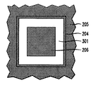
図3は、図2のボンド・パッド部分の一実施例の透視上面図を示す。第1パッシベーション層205とパッシベーション構造体206は、斜めの網目パターンを使用して示されている。パッシベーション層205が図3に示された領域を超えて広がっていることに留意すべきである。ボンド・パッド204は、形がほぼ正方形である。パッシベーション構造体206は、おおむね(i)ボンド・パッド204の領域内の中心に置かれ、(ii)形状が正方形である。ボンド・パッド204およびパッシベーション構造体206に関する具体例の寸法は、それぞれ60×60μmおよび40×40μmである。白で示される接続領域301は、パッシベーション構造体206と第1パッシベーション層205との間の区域である。接続領域301は、図2の最上部のメタライゼーション層M7へのボンド・パッド204の電気的接続を提供する。
FIG. 3 shows a perspective top view of one embodiment of the bond pad portion of FIG. The
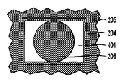
図4は、図2のボンド・パッド部分の別の実施例の透視上面図を示す。第1パッシベーション層205とパッシベーション構造体206は、斜めの網目パターンを使用して示されており、パッシベーション層205は示された領域を超えて広がっている。ボンド・パッド204は、おおむね長方形である。パッシベーション構造体206は、おおむね(i)ボンド・パッド204の領域内の中心に置かれ、(ii)形状が円形である。円形は、楕円形の特定のタイプであることに留意されたい。ボンド・パッド204およびパッシベーション構造体206に関する具体例の寸法は、それぞれ60×40μmおよび直径40μmである。白で示される接続領域401は、パッシベーション構造体206と第1パッシベーション層205との間の区域である。接続領域401は、図2の最上部のメタライゼーション層M7へのボンド・パッド204の電気的接続を提供する。
FIG. 4 shows a perspective top view of another embodiment of the bond pad portion of FIG. The
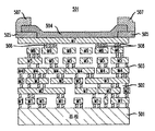
図5は、本発明の別の一実施形態による半導体デバイス500のボンド・パッドの断面図を示す。図2中の要素に実質的に同様である図5中の要素は、同様の形で番号を付けられているが、異なる接頭番号を有する。半導体デバイス500のボンド・パッド504は、図2のパッシベーション構造体206に類似したパッシベーション構造を含まない。その代わりに、構造的な補強は、メタライゼーション層M6とM7との間の、ビア508のような、サポート・ビアを使用して与えられる。ボンド・パッド504下側のメタライゼーション層M6の領域は、部分的に配線することを制限されており、ある部分は金属配線を配線するために使用されるが、別の部分はメタライゼーション層M7に接続された専用の金属配線を備え、ボンド・パッド504に対する構造的なサポートを提供する。それにも拘わらず、専用の金属配線がボンド・パッド504を基板501上の適切な構成要素に接続する導電経路の一部として使用され得ることに留意すべきである。
FIG. 5 illustrates a cross-sectional view of a bond pad of a semiconductor device 500 according to another embodiment of the present invention. Elements in FIG. 5 that are substantially similar to elements in FIG. 2 are numbered in a similar manner but have different prefix numbers. The
図6は、図5のボンド・パッド部分の一実施例の透視上面図を示す。第1パッシベーション層505は、斜めの網目パターンを使用して示されており、パッシベーション層505は示された領域を超えて広がっている。ボンド・パッド504は、おおむね正方形である。メタライゼーション層M6の配線制限領域601は、図5のビア508のような構造的−サポート・ビアに対応し、直交する網目パターンを使用して示されている。図6の配線制限領域601は、部分的骨組みを形成しており、ボンド・パッド504の中心に関してほぼ対称的である。
FIG. 6 shows a perspective top view of one embodiment of the bond pad portion of FIG. The
図5のボンド・パッド部分の別の実施例では、メタライゼーション層M6の配線制限領域601および対応する構造サポート・ビアは、図6に示されたもの以外の形状を形成する。ボンド・パッド504下側の領域におけるメタライゼーション層M6とM7との間のビアの占有密度、すなわち、金属ビアである上面図断面積の割合、は、少なくとも30%であるべきであり、約60%〜80%の好ましい占有密度である。その占有密度は、メタライゼーション層M6の専用金属配線を特別に配線すること、または相互接続する金属構成物に関する特別な占有パターンの使用のいずれかにより実現できる。
In another embodiment of the bond pad portion of FIG. 5, the
図4のボンド・パッド204の別の実施形態では、パッシベーション構造体206は、ボンド・パッド204の小さい方の寸法よりも小さな直径を有する。図2のボンド・パッド204の別の実施例では、パッシベーション構造体206は、真円でない楕円形の形状である。図2のボンド・パッド204の別の実施例では、パッシベーション構造体206は、正方形または楕円形以外の形状である。パッシベーション構造体206の具体的な形状の設計において、考慮されるべき要因は、半導体デバイスの設計ルール、パッシベーション構造体の面積を最大にして最大の構造的サポートを与えるという要求、および接触面積を最大にしてボンド・パッドから最上部のメタライゼーション層へ最大の信号伝送を与えるという要求、である。
In another embodiment of
図2の半導体デバイス200の1つの別の実施例では、ボンド・パッド204下側の領域においてメタライゼーション層M6とM7との間に何も金属ビアがない。
In one alternative embodiment of the semiconductor device 200 of FIG. 2, there are no metal vias between the metallization layers M6 and M7 in the region below the
半導体デバイスの実施形態を、メタライゼーション層を7つ有するものとして説明した。この個数は一例である。当業者により認識されるように、別の実施形態は、個々の半導体デバイスの設計者によって決定されるように、別の個数のメタライゼーション層を有することができる。 Semiconductor device embodiments have been described as having seven metallization layers. This number is an example. As will be appreciated by those skilled in the art, other embodiments may have a different number of metallization layers, as determined by the designer of the individual semiconductor device.
半導体デバイスの実施形態を、第2パッシベーション層を採用しているものとして説明した。ある別の実施形態は、第1パッシベーション層だけを有する。もう1つの別の実施形態は、3つ以上のパッシベーション層を有する。 Embodiments of the semiconductor device have been described as employing a second passivation layer. Certain other embodiments have only a first passivation layer. Another alternative embodiment has more than two passivation layers.
ある種の集積回路は、プローブ領域に直接接続されたボンド・パッドを有する1または複数の金属構造体を備える。本明細書において使用されるように、用語「ボンド・パッド」は、そのような金属構造体のプローブ領域を含まない。 Some integrated circuits comprise one or more metal structures having bond pads directly connected to the probe region. As used herein, the term “bond pad” does not include the probe region of such metal structures.
図2の半導体デバイス200の1つの別の実施例では、ボンド・パッド204とのコンタクト構造を形成するメタライゼーション層M7の配線制限部分は、図3の接続領域301または図4の接続領域401のような接続領域とほぼ類似の形状にされている。そのように、パッシベーション構造体の下側にあるメタライゼーション層M7のある領域は、金属配線を配線するために使用できる。例えば、1つの実施形態では、図3のパッシベーション構造体206に対応するメタライゼーション層M7の領域は、金属配線を通常に配線するために使用できる。
In one alternative embodiment of the semiconductor device 200 of FIG. 2, the wiring restriction portion of the metallization layer M7 that forms a contact structure with the
本発明の本質を説明するために記述および図示した構成要素の詳細、材料、および配置の様々な変更が、下記の特許請求の範囲において述べられるような本発明の範囲から乖離することなく当業者により行われ得ることが、さらに理解されるであろう。 Various changes in the details, materials, and arrangement of the components described and illustrated to illustrate the nature of the invention will be apparent to those skilled in the art without departing from the scope of the invention as set forth in the claims below. It will be further understood that this can be done by:
「1つの実施形態(one embodiment)」または「ある実施形態(an embodiment)」との本明細書における言及は、その実施形態に関係して説明される特有の構成、構造、または特徴が本発明の少なくとも1つの実施形態において含まれ得ることを意味する。明細書中の様々な場所において表現「1つの実施形態では」が現れることは、必ずしも全て同じ実施形態を引用しているのではなく、個々の実施形態または別の実施形態が他の実施形態を相互に除外しているのでもない。同じことは、用語「実施例(implementation)」にも適用される。 Reference herein to "one embodiment" or "an embodiment" refers to a particular configuration, structure, or feature that is described in connection with that embodiment. It can be included in at least one embodiment of The appearances of the phrase “in one embodiment” in various places in the specification are not necessarily all referring to the same embodiment, but an individual embodiment or another embodiment refers to another embodiment. They are not excluded from each other. The same applies to the term “implementation”.
明確に述べられない限りそれ以外は、それぞれの数値と範囲は、語「約(about)」または「ほぼ(approximately)」がその値または範囲の値の前にあたかもあるように、近似として解釈されるべきである。本出願において使用されるように、明確に指示されない限り、用語「接続された(connected)」は、要素間の直接接続および間接接続の両者を含むように意図されている。 Unless otherwise expressly stated, each numerical value and range is interpreted as an approximation, as if the word “about” or “approximately” preceded the value of the value or range. Should be. As used in this application, unless expressly indicated, the term “connected” is intended to include both direct and indirect connections between elements.
この説明の目的のために、用語「つなぐ(couple)」、「カップリング(coupling)」、「つながれた(coupled)」、「接続(する)(connect)」、「接続すること(connecting)」、または「接続された(connected)」は、エネルギーが2以上の要素間で伝達されることを可能にする、この分野において公知のまたは後で開発されるいずれかの方式を言及しており、必ずしも必要ではないが、1または複数の追加の要素の挿入が意図される。用語「直接つながれた」、「直接接続された」等は、接続された複数の要素が伝達されるエネルギーのために伝導体を介して接触しているまたは接続される、のいずれかを意味する。 For purposes of this description, the terms “couple”, “coupled”, “coupled”, “connect”, “connecting” Or “connected” refers to any scheme known or later developed in the art that allows energy to be transferred between two or more elements; Although not necessarily required, insertion of one or more additional elements is contemplated. The terms “directly connected”, “directly connected”, etc. mean that the connected elements are either in contact or connected via a conductor for the energy transferred. .
特許請求の範囲における図面番号および/または図面の参照符号の使用は、請求項の解釈を容易にするために特許請求される事項の1または複数の可能な実施形態を特定するように意図されている。係る使用は、対応する図面に示される実施形態にこれらの請求項の範囲を制限するように解釈されるべきではない。 The use of drawing numbers and / or reference signs in the claims is intended to identify one or more possible embodiments of the claimed subject matter in order to facilitate the interpretation of the claims. Yes. Such use is not to be construed as limiting the scope of these claims to the embodiments shown in the corresponding drawings.
Claims (10)
前記ボンド・パッドの直ぐ下側にあり前記ボンド・パッドの第1部分に直接接触する第1パッシベーション構造体(例えば、206)と、
前記ボンド・パッド及び前記第1パッシベーション構造体の下の第1メタライゼーション層(例えば、M7)であって、(i)前記ボンド・パッドの第2部分及び(ii)前記第1パッシベーション構造体の両者の直ぐ下側にありこの両者と直接接触している第1金属構造体を備える、第1メタライゼーション層(例えば、M7)と、
前記第1メタライゼーション層の下の第2メタライゼーション層(例えば、M6)と、
前記第1メタライゼーション層と前記第2メタライゼーション層との間の第1誘電体材料と、を備え、前記第2メタライゼーション層で前記ボンド・パッドの直ぐ下側の部分は、2以上の別個の配線経路に対応する2以上の金属構造体を備える、
集積回路(IC)。 A bond pad (eg, 204);
A first passivation structure (eg, 206) directly under the bond pad and in direct contact with the first portion of the bond pad;
A first metallization layer (e.g., M7) below the bond pad and the first passivation structure, comprising: (i) a second portion of the bond pad; and (ii) of the first passivation structure. A first metallization layer (e.g., M7) comprising a first metal structure immediately below and in direct contact with both;
A second metallization layer (eg, M6) below the first metallization layer;
A first dielectric material between the first metallization layer and the second metallization layer, wherein the portion of the second metallization layer immediately below the bond pad is two or more distinct Comprising two or more metal structures corresponding to the wiring path of
Integrated circuit (IC).
Applications Claiming Priority (1)
| Application Number | Priority Date | Filing Date | Title |
|---|---|---|---|
| PCT/US2007/083183 WO2009058143A1 (en) | 2007-10-31 | 2007-10-31 | Bond pad support structure for semiconductor device |
Publications (2)
| Publication Number | Publication Date |
|---|---|
| JP2011502352A true JP2011502352A (en) | 2011-01-20 |
| JP2011502352A5 JP2011502352A5 (en) | 2011-10-20 |
Family
ID=39523612
Family Applications (1)
| Application Number | Title | Priority Date | Filing Date |
|---|---|---|---|
| JP2010530988A Pending JP2011502352A (en) | 2007-10-31 | 2007-10-31 | Bond pad support structure for semiconductor devices |
Country Status (5)
| Country | Link |
|---|---|
| US (1) | US8183698B2 (en) |
| EP (2) | EP2568498A3 (en) |
| JP (1) | JP2011502352A (en) |
| KR (1) | KR101360815B1 (en) |
| WO (1) | WO2009058143A1 (en) |
Families Citing this family (27)
| Publication number | Priority date | Publication date | Assignee | Title |
|---|---|---|---|---|
| US7888257B2 (en) | 2007-10-10 | 2011-02-15 | Agere Systems Inc. | Integrated circuit package including wire bonds |
| KR101360815B1 (en) | 2007-10-31 | 2014-02-11 | 에이저 시스템즈 엘엘시 | Bond pad support structure for semiconductor device |
| JP5362296B2 (en) * | 2008-09-03 | 2013-12-11 | 矢崎総業株式会社 | Terminal fitting |
| KR20110056005A (en) * | 2009-11-20 | 2011-05-26 | 삼성전자주식회사 | Interconnection structures of semiconductor device |
| JP5730062B2 (en) | 2011-02-21 | 2015-06-03 | 株式会社ジャパンディスプレイ | Display device |
| WO2011107044A2 (en) * | 2011-04-19 | 2011-09-09 | 华为技术有限公司 | Waterproof structure for bonding pad, waterproof bonding pad and method for forming waterproof structure |
| US8435824B2 (en) * | 2011-07-07 | 2013-05-07 | Taiwan Semiconductor Manufacturing Company, Ltd. | Backside illumination sensor having a bonding pad structure and method of making the same |
| US8994181B2 (en) * | 2011-08-18 | 2015-03-31 | Taiwan Semiconductor Manufacturing Company, Ltd. | Bond pad structure to reduce bond pad corrosion |
| ITMI20111568A1 (en) * | 2011-08-31 | 2013-03-01 | St Microelectronics Srl | MONITORING STRUCTURE OF A CONNECTION PAD AND ITS RELATIVE METHOD OF DETECTION OF SIGNIFICANT ALTERATIONS |
| US9064707B2 (en) * | 2011-09-14 | 2015-06-23 | Micronas Gmbh | Bonding contact area on a semiconductor substrate |
| US20130241058A1 (en) * | 2012-03-16 | 2013-09-19 | Taiwan Semiconductor Manufacturing Company, Ltd. | Wire Bonding Structures for Integrated Circuits |
| US9166054B2 (en) * | 2012-04-13 | 2015-10-20 | Semiconductor Energy Laboratory Co., Ltd. | Semiconductor device and manufacturing method thereof |
| KR101933015B1 (en) | 2012-04-19 | 2018-12-27 | 삼성전자주식회사 | Pad structure of a semiconductor device, method of manufacturing the pad structure and semiconductor package including the pad structure |
| US20130320522A1 (en) * | 2012-05-30 | 2013-12-05 | Taiwan Semiconductor Manufacturing Company, Ltd. | Re-distribution Layer Via Structure and Method of Making Same |
| US9455226B2 (en) | 2013-02-01 | 2016-09-27 | Mediatek Inc. | Semiconductor device allowing metal layer routing formed directly under metal pad |
| US9536833B2 (en) | 2013-02-01 | 2017-01-03 | Mediatek Inc. | Semiconductor device allowing metal layer routing formed directly under metal pad |
| CN104952822A (en) * | 2014-03-25 | 2015-09-30 | 中芯国际集成电路制造(上海)有限公司 | Welding pad structure |
| US9245846B2 (en) * | 2014-05-06 | 2016-01-26 | International Business Machines Corporation | Chip with programmable shelf life |
| US9960130B2 (en) | 2015-02-06 | 2018-05-01 | UTAC Headquarters Pte. Ltd. | Reliable interconnect |
| EP3131118B1 (en) * | 2015-08-12 | 2019-04-17 | MediaTek Inc. | Semiconductor device allowing metal layer routing formed directly under metal pad |
| US9922947B2 (en) * | 2016-04-28 | 2018-03-20 | Stmicroelectronics S.R.L. | Bonding pad structure over active circuitry |
| US10896885B2 (en) * | 2017-09-13 | 2021-01-19 | Polar Semiconductor, Llc | High-voltage MOSFET structures |
| US11705395B2 (en) * | 2018-06-25 | 2023-07-18 | Intel Corporation | Core fill to reduce dishing and metal pillar fill to increase metal density of interconnects |
| TWI731431B (en) * | 2019-10-04 | 2021-06-21 | 旺宏電子股份有限公司 | Pad structure |
| US11348883B2 (en) * | 2020-03-27 | 2022-05-31 | Texas Instruments Incorporated | High voltage isolation barrier with electric overstress integrity |
| US11243573B2 (en) * | 2020-04-28 | 2022-02-08 | Taiwan Semiconductor Manufacturing Company, Ltd. | Semiconductor package, display apparatus and manufacturing method of semiconductor package |
| JP2022051283A (en) * | 2020-09-18 | 2022-03-31 | 新光電気工業株式会社 | Wiring board and manufacturing method of the same |
Citations (2)
| Publication number | Priority date | Publication date | Assignee | Title |
|---|---|---|---|---|
| JPH06275794A (en) * | 1993-03-18 | 1994-09-30 | Matsushita Electric Ind Co Ltd | Semiconductor storage device and its manufacture |
| JP2007227827A (en) * | 2006-02-27 | 2007-09-06 | Elpida Memory Inc | Semiconductor device |
Family Cites Families (68)
| Publication number | Priority date | Publication date | Assignee | Title |
|---|---|---|---|---|
| US5302550A (en) * | 1985-12-24 | 1994-04-12 | Mitsubishi Denki Kabushiki Kaisha | Method of bonding a microelectronic device |
| US5106461A (en) * | 1989-04-04 | 1992-04-21 | Massachusetts Institute Of Technology | High-density, multi-level interconnects, flex circuits, and tape for tab |
| US5128737A (en) * | 1990-03-02 | 1992-07-07 | Silicon Dynamics, Inc. | Semiconductor integrated circuit fabrication yield improvements |
| US5248903A (en) * | 1992-09-18 | 1993-09-28 | Lsi Logic Corporation | Composite bond pads for semiconductor devices |
| EP0637840A1 (en) * | 1993-08-05 | 1995-02-08 | AT&T Corp. | Integrated circuit with active devices under bond pads |
| US5656858A (en) * | 1994-10-19 | 1997-08-12 | Nippondenso Co., Ltd. | Semiconductor device with bump structure |
| US5659201A (en) * | 1995-06-05 | 1997-08-19 | Advanced Micro Devices, Inc. | High conductivity interconnection line |
| US5686762A (en) * | 1995-12-21 | 1997-11-11 | Micron Technology, Inc. | Semiconductor device with improved bond pads |
| DE19609229C2 (en) * | 1996-03-09 | 1998-10-15 | Micronas Intermetall Gmbh | Method of making discrete electronic elements |
| US5854514A (en) * | 1996-08-05 | 1998-12-29 | International Buisness Machines Corporation | Lead-free interconnection for electronic devices |
| JP3526376B2 (en) * | 1996-08-21 | 2004-05-10 | 株式会社東芝 | Semiconductor device and manufacturing method thereof |
| KR100230428B1 (en) * | 1997-06-24 | 1999-11-15 | 윤종용 | Semiconductor device comprising a multi-conductive pad and method for manufacturing the same |
| US6100184A (en) * | 1997-08-20 | 2000-08-08 | Sematech, Inc. | Method of making a dual damascene interconnect structure using low dielectric constant material for an inter-level dielectric layer |
| US6103552A (en) * | 1998-08-10 | 2000-08-15 | Lin; Mou-Shiung | Wafer scale packaging scheme |
| US6187680B1 (en) * | 1998-10-07 | 2001-02-13 | International Business Machines Corporation | Method/structure for creating aluminum wirebound pad on copper BEOL |
| US8021976B2 (en) * | 2002-10-15 | 2011-09-20 | Megica Corporation | Method of wire bonding over active area of a semiconductor circuit |
| US6358831B1 (en) * | 1999-03-03 | 2002-03-19 | Taiwan Semiconductor Manufacturing Company | Method for forming a top interconnection level and bonding pads on an integrated circuit chip |
| KR20010004529A (en) * | 1999-06-29 | 2001-01-15 | 김영환 | wafer level package and method of fabricating the same |
| JP4021104B2 (en) * | 1999-08-05 | 2007-12-12 | セイコーインスツル株式会社 | Semiconductor device having bump electrodes |
| US6803302B2 (en) * | 1999-11-22 | 2004-10-12 | Freescale Semiconductor, Inc. | Method for forming a semiconductor device having a mechanically robust pad interface |
| US6198170B1 (en) * | 1999-12-16 | 2001-03-06 | Conexant Systems, Inc. | Bonding pad and support structure and method for their fabrication |
| KR100386081B1 (en) * | 2000-01-05 | 2003-06-09 | 주식회사 하이닉스반도체 | Semiconductor package and fabricating method thereof |
| US6306750B1 (en) * | 2000-01-18 | 2001-10-23 | Taiwan Semiconductor Manufacturing Company | Bonding pad structure to prevent inter-metal dielectric cracking and to improve bondability |
| US6495917B1 (en) * | 2000-03-17 | 2002-12-17 | International Business Machines Corporation | Method and structure of column interconnect |
| US6620720B1 (en) * | 2000-04-10 | 2003-09-16 | Agere Systems Inc | Interconnections to copper IC's |
| JP2002016069A (en) * | 2000-06-29 | 2002-01-18 | Matsushita Electric Ind Co Ltd | Semiconductor device and its manufacturing method |
| US6440833B1 (en) * | 2000-07-19 | 2002-08-27 | Taiwan Semiconductor Manufacturing Company | Method of protecting a copper pad structure during a fuse opening procedure |
| US6426556B1 (en) * | 2001-01-16 | 2002-07-30 | Megic Corporation | Reliable metal bumps on top of I/O pads with test probe marks |
| US7242099B2 (en) * | 2001-03-05 | 2007-07-10 | Megica Corporation | Chip package with multiple chips connected by bumps |
| JP2002324797A (en) * | 2001-04-24 | 2002-11-08 | Mitsubishi Electric Corp | Semiconductor device and method of manufacturing the same |
| US6732913B2 (en) * | 2001-04-26 | 2004-05-11 | Advanpack Solutions Pte Ltd. | Method for forming a wafer level chip scale package, and package formed thereby |
| US6689680B2 (en) * | 2001-07-14 | 2004-02-10 | Motorola, Inc. | Semiconductor device and method of formation |
| KR100423906B1 (en) * | 2001-08-08 | 2004-03-22 | 삼성전자주식회사 | Ferroelectric memory device amd method of forming the same |
| US6531384B1 (en) * | 2001-09-14 | 2003-03-11 | Motorola, Inc. | Method of forming a bond pad and structure thereof |
| US6614091B1 (en) | 2002-03-13 | 2003-09-02 | Motorola, Inc. | Semiconductor device having a wire bond pad and method therefor |
| US6844631B2 (en) * | 2002-03-13 | 2005-01-18 | Freescale Semiconductor, Inc. | Semiconductor device having a bond pad and method therefor |
| TW544884B (en) * | 2002-04-03 | 2003-08-01 | Advanced Semiconductor Eng | Chip structure and wire-bonding process suited for the same |
| JP2003347351A (en) * | 2002-05-29 | 2003-12-05 | Mitsubishi Electric Corp | Semiconductor device |
| JP3967199B2 (en) * | 2002-06-04 | 2007-08-29 | シャープ株式会社 | Semiconductor device and manufacturing method thereof |
| US6642597B1 (en) * | 2002-10-16 | 2003-11-04 | Lsi Logic Corporation | Inter-layer interconnection structure for large electrical connections |
| US7328830B2 (en) * | 2002-12-20 | 2008-02-12 | Agere Systems Inc. | Structure and method for bonding to copper interconnect structures |
| JP2004207509A (en) | 2002-12-25 | 2004-07-22 | Matsushita Electric Ind Co Ltd | Semiconductor device and manufacturing method thereof |
| US20040124546A1 (en) * | 2002-12-29 | 2004-07-01 | Mukul Saran | Reliable integrated circuit and package |
| US6959856B2 (en) * | 2003-01-10 | 2005-11-01 | Samsung Electronics Co., Ltd. | Solder bump structure and method for forming a solder bump |
| US6864578B2 (en) * | 2003-04-03 | 2005-03-08 | International Business Machines Corporation | Internally reinforced bond pads |
| US6717270B1 (en) * | 2003-04-09 | 2004-04-06 | Motorola, Inc. | Integrated circuit die I/O cells |
| US7566964B2 (en) * | 2003-04-10 | 2009-07-28 | Agere Systems Inc. | Aluminum pad power bus and signal routing for integrated circuit devices utilizing copper technology interconnect structures |
| US6844626B2 (en) * | 2003-05-23 | 2005-01-18 | Taiwan Semiconductor Manufacturing Company, Ltd. | Bond pad scheme for Cu process |
| US6798035B1 (en) * | 2003-06-20 | 2004-09-28 | Lsi Logic Corporation | Bonding pad for low k dielectric |
| US7005369B2 (en) * | 2003-08-21 | 2006-02-28 | Intersil American Inc. | Active area bonding compatible high current structures |
| US6743979B1 (en) * | 2003-08-29 | 2004-06-01 | Lsi Logic Corporation | Bonding pad isolation |
| US6825563B1 (en) * | 2003-10-09 | 2004-11-30 | Lsi Logic Corporation | Slotted bonding pad |
| US7057296B2 (en) * | 2003-10-29 | 2006-06-06 | Taiwan Semiconductor Manufacturing Co., Ltd. | Bonding pad structure |
| US7049170B2 (en) * | 2003-12-17 | 2006-05-23 | Tru-Si Technologies, Inc. | Integrated circuits and packaging substrates with cavities, and attachment methods including insertion of protruding contact pads into cavities |
| US7242102B2 (en) * | 2004-07-08 | 2007-07-10 | Spansion Llc | Bond pad structure for copper metallization having increased reliability and method for fabricating same |
| US7115985B2 (en) * | 2004-09-30 | 2006-10-03 | Agere Systems, Inc. | Reinforced bond pad for a semiconductor device |
| US20060091566A1 (en) * | 2004-11-02 | 2006-05-04 | Chin-Tien Yang | Bond pad structure for integrated circuit chip |
| US7241636B2 (en) * | 2005-01-11 | 2007-07-10 | Freescale Semiconductor, Inc. | Method and apparatus for providing structural support for interconnect pad while allowing signal conductance |
| US7364998B2 (en) * | 2005-07-21 | 2008-04-29 | Taiwan Semiconductor Manufacturing Co., Ltd. | Method for forming high reliability bump structure |
| US7535114B2 (en) * | 2005-12-13 | 2009-05-19 | Intel Corporation | Integrated circuit devices including compliant material under bond pads and methods of fabrication |
| JP2007227815A (en) | 2006-02-27 | 2007-09-06 | Consortium For Advanced Semiconductor Materials & Related Technologies | Element for evaluating bonding resistance |
| US7592710B2 (en) * | 2006-03-03 | 2009-09-22 | Taiwan Semiconductor Manufacturing Company, Ltd. | Bond pad structure for wire bonding |
| US7955973B2 (en) * | 2006-08-01 | 2011-06-07 | Freescale Semiconductor, Inc. | Method and apparatus for improvements in chip manufacture and design |
| KR100772903B1 (en) * | 2006-10-23 | 2007-11-05 | 삼성전자주식회사 | Semiconductor device and method for fabricating the same |
| US20080272487A1 (en) * | 2007-05-04 | 2008-11-06 | Il Kwon Shim | System for implementing hard-metal wire bonds |
| US7622737B2 (en) * | 2007-07-11 | 2009-11-24 | International Business Machines Corporation | Test structures for electrically detecting back end of the line failures and methods of making and using the same |
| US20090079082A1 (en) * | 2007-09-24 | 2009-03-26 | Yong Liu | Bonding pad structure allowing wire bonding over an active area in a semiconductor die and method of manufacturing same |
| KR101360815B1 (en) | 2007-10-31 | 2014-02-11 | 에이저 시스템즈 엘엘시 | Bond pad support structure for semiconductor device |
-
2007
- 2007-10-31 KR KR1020107007877A patent/KR101360815B1/en active IP Right Grant
- 2007-10-31 WO PCT/US2007/083183 patent/WO2009058143A1/en active Application Filing
- 2007-10-31 EP EP20120195715 patent/EP2568498A3/en not_active Ceased
- 2007-10-31 JP JP2010530988A patent/JP2011502352A/en active Pending
- 2007-10-31 EP EP07854541A patent/EP2195837A1/en not_active Withdrawn
- 2007-10-31 US US12/678,405 patent/US8183698B2/en active Active
Patent Citations (2)
| Publication number | Priority date | Publication date | Assignee | Title |
|---|---|---|---|---|
| JPH06275794A (en) * | 1993-03-18 | 1994-09-30 | Matsushita Electric Ind Co Ltd | Semiconductor storage device and its manufacture |
| JP2007227827A (en) * | 2006-02-27 | 2007-09-06 | Elpida Memory Inc | Semiconductor device |
Also Published As
| Publication number | Publication date |
|---|---|
| EP2568498A3 (en) | 2013-04-24 |
| EP2195837A1 (en) | 2010-06-16 |
| KR101360815B1 (en) | 2014-02-11 |
| US8183698B2 (en) | 2012-05-22 |
| WO2009058143A1 (en) | 2009-05-07 |
| KR20100077161A (en) | 2010-07-07 |
| EP2568498A2 (en) | 2013-03-13 |
| US20100201000A1 (en) | 2010-08-12 |
Similar Documents
| Publication | Publication Date | Title |
|---|---|---|
| JP2011502352A (en) | Bond pad support structure for semiconductor devices | |
| US7241636B2 (en) | Method and apparatus for providing structural support for interconnect pad while allowing signal conductance | |
| US5986343A (en) | Bond pad design for integrated circuits | |
| US7834435B2 (en) | Leadframe with extended pad segments between leads and die pad, and leadframe package using the same | |
| US6462427B2 (en) | Semiconductor chip, set of semiconductor chips and multichip module | |
| US20130334705A1 (en) | Semiconductor device | |
| EP2731134A1 (en) | Multi-chip module connection by way of bridging blocks | |
| US20070249153A1 (en) | Chip structure with half-tunneling electrical contact to have one electrical contact formed on inactive side thereof and method for producing the same | |
| US7741716B1 (en) | Integrated circuit bond pad structures | |
| US20120146216A1 (en) | Semiconductor package and fabrication method thereof | |
| JP3651346B2 (en) | Semiconductor device and manufacturing method thereof | |
| JP2003243437A (en) | Air pad solder joining structure of wafer level package and manufacturing method thereof | |
| US20060115930A1 (en) | Semiconductor device and method of fabricating the same, circuit board, and electronic instrument | |
| TWI578476B (en) | Semiconductor package | |
| KR101123804B1 (en) | Semiconductor chip and stacked semiconductor package havng the same | |
| US20060091566A1 (en) | Bond pad structure for integrated circuit chip | |
| KR100712517B1 (en) | Interposer of semiconductor device having air gap structure | |
| US9646941B2 (en) | Semiconductor packaging device including via-in pad (VIP) and manufacturing method thereof | |
| JP5511119B2 (en) | Interposer and semiconductor device | |
| US20080164601A1 (en) | Chip package structure | |
| US20040155357A1 (en) | [chip package structure and manufacturing process thereof] | |
| EP1310996A2 (en) | Direct interconnect multi-chip module, method for making the same and electronic package comprising same | |
| US10256201B2 (en) | Bonding pad structure having island portions and method for manufacturing the same | |
| TWI385774B (en) | Leadframe package and leadframe | |
| CN106158775A (en) | Semiconductor package and manufacture method thereof |
Legal Events
| Date | Code | Title | Description |
|---|---|---|---|
| A521 | Written amendment |
Free format text: JAPANESE INTERMEDIATE CODE: A523 Effective date: 20110826 |
|
| RD04 | Notification of resignation of power of attorney |
Free format text: JAPANESE INTERMEDIATE CODE: A7424 Effective date: 20120710 |
|
| A977 | Report on retrieval |
Free format text: JAPANESE INTERMEDIATE CODE: A971007 Effective date: 20120823 |
|
| A131 | Notification of reasons for refusal |
Free format text: JAPANESE INTERMEDIATE CODE: A131 Effective date: 20120904 |
|
| A601 | Written request for extension of time |
Free format text: JAPANESE INTERMEDIATE CODE: A601 Effective date: 20121204 |
|
| A602 | Written permission of extension of time |
Free format text: JAPANESE INTERMEDIATE CODE: A602 Effective date: 20121211 |
|
| A521 | Written amendment |
Free format text: JAPANESE INTERMEDIATE CODE: A523 Effective date: 20130304 |
|
| A02 | Decision of refusal |
Free format text: JAPANESE INTERMEDIATE CODE: A02 Effective date: 20130418 |
|
| A521 | Written amendment |
Free format text: JAPANESE INTERMEDIATE CODE: A523 Effective date: 20130819 |
|
| A911 | Transfer to examiner for re-examination before appeal (zenchi) |
Free format text: JAPANESE INTERMEDIATE CODE: A911 Effective date: 20131002 |
|
| A912 | Re-examination (zenchi) completed and case transferred to appeal board |
Free format text: JAPANESE INTERMEDIATE CODE: A912 Effective date: 20131122 |
|
| A601 | Written request for extension of time |
Free format text: JAPANESE INTERMEDIATE CODE: A601 Effective date: 20140319 |
|
| A602 | Written permission of extension of time |
Free format text: JAPANESE INTERMEDIATE CODE: A602 Effective date: 20140325 |
|
| RD03 | Notification of appointment of power of attorney |
Free format text: JAPANESE INTERMEDIATE CODE: A7423 Effective date: 20140729 |
|
| RD04 | Notification of resignation of power of attorney |
Free format text: JAPANESE INTERMEDIATE CODE: A7424 Effective date: 20140805 |