JP2011500369A - Atmospheric pressure plasma treatment of printer components - Google Patents
Atmospheric pressure plasma treatment of printer components Download PDFInfo
- Publication number
- JP2011500369A JP2011500369A JP2010529919A JP2010529919A JP2011500369A JP 2011500369 A JP2011500369 A JP 2011500369A JP 2010529919 A JP2010529919 A JP 2010529919A JP 2010529919 A JP2010529919 A JP 2010529919A JP 2011500369 A JP2011500369 A JP 2011500369A
- Authority
- JP
- Japan
- Prior art keywords
- component
- electrode
- printer
- microplasma
- electrodes
- Prior art date
- Legal status (The legal status is an assumption and is not a legal conclusion. Google has not performed a legal analysis and makes no representation as to the accuracy of the status listed.)
- Withdrawn
Links
- 238000009832 plasma treatment Methods 0.000 title description 12
- 238000000034 method Methods 0.000 claims abstract description 97
- 238000012545 processing Methods 0.000 claims abstract description 48
- 230000007246 mechanism Effects 0.000 claims description 17
- 230000006870 function Effects 0.000 claims description 12
- 239000007788 liquid Substances 0.000 claims description 12
- 230000015572 biosynthetic process Effects 0.000 claims description 9
- 230000008569 process Effects 0.000 abstract description 33
- 239000012530 fluid Substances 0.000 description 62
- 239000007789 gas Substances 0.000 description 61
- 238000000576 coating method Methods 0.000 description 32
- 239000000463 material Substances 0.000 description 30
- 239000011248 coating agent Substances 0.000 description 28
- 238000007639 printing Methods 0.000 description 20
- 239000004065 semiconductor Substances 0.000 description 16
- 238000004140 cleaning Methods 0.000 description 14
- 229910052751 metal Inorganic materials 0.000 description 14
- 239000002184 metal Substances 0.000 description 14
- 238000011282 treatment Methods 0.000 description 11
- 239000010408 film Substances 0.000 description 10
- 239000000126 substance Substances 0.000 description 10
- OKTJSMMVPCPJKN-UHFFFAOYSA-N Carbon Chemical compound [C] OKTJSMMVPCPJKN-UHFFFAOYSA-N 0.000 description 9
- 238000004519 manufacturing process Methods 0.000 description 9
- 229910052799 carbon Inorganic materials 0.000 description 8
- 239000013626 chemical specie Substances 0.000 description 8
- 239000004020 conductor Substances 0.000 description 7
- 150000002500 ions Chemical class 0.000 description 7
- 229920000642 polymer Polymers 0.000 description 7
- 238000011084 recovery Methods 0.000 description 7
- VYPSYNLAJGMNEJ-UHFFFAOYSA-N Silicium dioxide Chemical compound O=[Si]=O VYPSYNLAJGMNEJ-UHFFFAOYSA-N 0.000 description 6
- XUIMIQQOPSSXEZ-UHFFFAOYSA-N Silicon Chemical compound [Si] XUIMIQQOPSSXEZ-UHFFFAOYSA-N 0.000 description 6
- 230000009471 action Effects 0.000 description 6
- 239000002131 composite material Substances 0.000 description 6
- 239000003989 dielectric material Substances 0.000 description 6
- 230000005684 electric field Effects 0.000 description 6
- 238000005530 etching Methods 0.000 description 6
- 238000007667 floating Methods 0.000 description 6
- 238000007641 inkjet printing Methods 0.000 description 6
- 239000000203 mixture Substances 0.000 description 6
- 238000000623 plasma-assisted chemical vapour deposition Methods 0.000 description 6
- 230000005855 radiation Effects 0.000 description 6
- 229910052710 silicon Inorganic materials 0.000 description 6
- 239000010703 silicon Substances 0.000 description 6
- 229910052782 aluminium Inorganic materials 0.000 description 5
- XAGFODPZIPBFFR-UHFFFAOYSA-N aluminium Chemical compound [Al] XAGFODPZIPBFFR-UHFFFAOYSA-N 0.000 description 5
- 239000012159 carrier gas Substances 0.000 description 5
- 230000015556 catabolic process Effects 0.000 description 5
- 230000004048 modification Effects 0.000 description 5
- 238000012986 modification Methods 0.000 description 5
- 230000009257 reactivity Effects 0.000 description 5
- 229910052715 tantalum Inorganic materials 0.000 description 5
- GUVRBAGPIYLISA-UHFFFAOYSA-N tantalum atom Chemical compound [Ta] GUVRBAGPIYLISA-UHFFFAOYSA-N 0.000 description 5
- 229910052581 Si3N4 Inorganic materials 0.000 description 4
- QVGXLLKOCUKJST-UHFFFAOYSA-N atomic oxygen Chemical compound [O] QVGXLLKOCUKJST-UHFFFAOYSA-N 0.000 description 4
- 230000004888 barrier function Effects 0.000 description 4
- 230000000694 effects Effects 0.000 description 4
- PCHJSUWPFVWCPO-UHFFFAOYSA-N gold Chemical compound [Au] PCHJSUWPFVWCPO-UHFFFAOYSA-N 0.000 description 4
- 229910052737 gold Inorganic materials 0.000 description 4
- 239000010931 gold Substances 0.000 description 4
- 239000001307 helium Substances 0.000 description 4
- 229910052734 helium Inorganic materials 0.000 description 4
- SWQJXJOGLNCZEY-UHFFFAOYSA-N helium atom Chemical compound [He] SWQJXJOGLNCZEY-UHFFFAOYSA-N 0.000 description 4
- 150000002430 hydrocarbons Chemical class 0.000 description 4
- 230000002209 hydrophobic effect Effects 0.000 description 4
- 230000010354 integration Effects 0.000 description 4
- 150000002739 metals Chemical class 0.000 description 4
- 238000004377 microelectronic Methods 0.000 description 4
- 239000001301 oxygen Substances 0.000 description 4
- 229910052760 oxygen Inorganic materials 0.000 description 4
- 239000012071 phase Substances 0.000 description 4
- HQVNEWCFYHHQES-UHFFFAOYSA-N silicon nitride Chemical compound N12[Si]34N5[Si]62N3[Si]51N64 HQVNEWCFYHHQES-UHFFFAOYSA-N 0.000 description 4
- 229910052814 silicon oxide Inorganic materials 0.000 description 4
- 239000007787 solid Substances 0.000 description 4
- IJGRMHOSHXDMSA-UHFFFAOYSA-N Atomic nitrogen Chemical compound N#N IJGRMHOSHXDMSA-UHFFFAOYSA-N 0.000 description 3
- 239000004215 Carbon black (E152) Substances 0.000 description 3
- 239000004593 Epoxy Substances 0.000 description 3
- CBENFWSGALASAD-UHFFFAOYSA-N Ozone Chemical compound [O-][O+]=O CBENFWSGALASAD-UHFFFAOYSA-N 0.000 description 3
- 239000004809 Teflon Substances 0.000 description 3
- 229920006362 Teflon® Polymers 0.000 description 3
- 238000000429 assembly Methods 0.000 description 3
- 230000000712 assembly Effects 0.000 description 3
- 230000009286 beneficial effect Effects 0.000 description 3
- 239000000919 ceramic Substances 0.000 description 3
- 238000003776 cleavage reaction Methods 0.000 description 3
- 230000006837 decompression Effects 0.000 description 3
- 238000000151 deposition Methods 0.000 description 3
- 239000003599 detergent Substances 0.000 description 3
- 238000010586 diagram Methods 0.000 description 3
- 239000006185 dispersion Substances 0.000 description 3
- 229930195733 hydrocarbon Natural products 0.000 description 3
- 238000000059 patterning Methods 0.000 description 3
- 229920002120 photoresistant polymer Polymers 0.000 description 3
- 230000007017 scission Effects 0.000 description 3
- HBMJWWWQQXIZIP-UHFFFAOYSA-N silicon carbide Chemical class [Si+]#[C-] HBMJWWWQQXIZIP-UHFFFAOYSA-N 0.000 description 3
- 229910010271 silicon carbide Inorganic materials 0.000 description 3
- 241000894007 species Species 0.000 description 3
- 239000000758 substrate Substances 0.000 description 3
- 229910052845 zircon Inorganic materials 0.000 description 3
- GFQYVLUOOAAOGM-UHFFFAOYSA-N zirconium(iv) silicate Chemical compound [Zr+4].[O-][Si]([O-])([O-])[O-] GFQYVLUOOAAOGM-UHFFFAOYSA-N 0.000 description 3
- QGZKDVFQNNGYKY-UHFFFAOYSA-N Ammonia Chemical compound N QGZKDVFQNNGYKY-UHFFFAOYSA-N 0.000 description 2
- XKRFYHLGVUSROY-UHFFFAOYSA-N Argon Chemical compound [Ar] XKRFYHLGVUSROY-UHFFFAOYSA-N 0.000 description 2
- ZOXJGFHDIHLPTG-UHFFFAOYSA-N Boron Chemical compound [B] ZOXJGFHDIHLPTG-UHFFFAOYSA-N 0.000 description 2
- RYGMFSIKBFXOCR-UHFFFAOYSA-N Copper Chemical compound [Cu] RYGMFSIKBFXOCR-UHFFFAOYSA-N 0.000 description 2
- YCKRFDGAMUMZLT-UHFFFAOYSA-N Fluorine atom Chemical compound [F] YCKRFDGAMUMZLT-UHFFFAOYSA-N 0.000 description 2
- 239000004642 Polyimide Substances 0.000 description 2
- BQCADISMDOOEFD-UHFFFAOYSA-N Silver Chemical compound [Ag] BQCADISMDOOEFD-UHFFFAOYSA-N 0.000 description 2
- RTAQQCXQSZGOHL-UHFFFAOYSA-N Titanium Chemical compound [Ti] RTAQQCXQSZGOHL-UHFFFAOYSA-N 0.000 description 2
- XLOMVQKBTHCTTD-UHFFFAOYSA-N Zinc monoxide Chemical compound [Zn]=O XLOMVQKBTHCTTD-UHFFFAOYSA-N 0.000 description 2
- 230000002159 abnormal effect Effects 0.000 description 2
- 238000013459 approach Methods 0.000 description 2
- 238000004380 ashing Methods 0.000 description 2
- 238000002417 atmospheric pressure glow discharge ionisation Methods 0.000 description 2
- 230000008901 benefit Effects 0.000 description 2
- 230000005540 biological transmission Effects 0.000 description 2
- 229910052796 boron Inorganic materials 0.000 description 2
- 210000004027 cell Anatomy 0.000 description 2
- 238000007385 chemical modification Methods 0.000 description 2
- 229920001940 conductive polymer Polymers 0.000 description 2
- 238000011109 contamination Methods 0.000 description 2
- 229910052802 copper Inorganic materials 0.000 description 2
- 239000010949 copper Substances 0.000 description 2
- 238000001514 detection method Methods 0.000 description 2
- 238000005516 engineering process Methods 0.000 description 2
- 238000011049 filling Methods 0.000 description 2
- 229910052731 fluorine Inorganic materials 0.000 description 2
- 239000011737 fluorine Substances 0.000 description 2
- 229920002313 fluoropolymer Polymers 0.000 description 2
- 239000011521 glass Substances 0.000 description 2
- AMGQUBHHOARCQH-UHFFFAOYSA-N indium;oxotin Chemical compound [In].[Sn]=O AMGQUBHHOARCQH-UHFFFAOYSA-N 0.000 description 2
- 238000012544 monitoring process Methods 0.000 description 2
- 230000007935 neutral effect Effects 0.000 description 2
- 229910052758 niobium Inorganic materials 0.000 description 2
- 239000010955 niobium Substances 0.000 description 2
- GUCVJGMIXFAOAE-UHFFFAOYSA-N niobium atom Chemical compound [Nb] GUCVJGMIXFAOAE-UHFFFAOYSA-N 0.000 description 2
- 150000004767 nitrides Chemical class 0.000 description 2
- 229910052756 noble gas Inorganic materials 0.000 description 2
- 230000001590 oxidative effect Effects 0.000 description 2
- TWNQGVIAIRXVLR-UHFFFAOYSA-N oxo(oxoalumanyloxy)alumane Chemical compound O=[Al]O[Al]=O TWNQGVIAIRXVLR-UHFFFAOYSA-N 0.000 description 2
- 239000002245 particle Substances 0.000 description 2
- 238000001020 plasma etching Methods 0.000 description 2
- BASFCYQUMIYNBI-UHFFFAOYSA-N platinum Chemical compound [Pt] BASFCYQUMIYNBI-UHFFFAOYSA-N 0.000 description 2
- 229920001721 polyimide Polymers 0.000 description 2
- 238000006116 polymerization reaction Methods 0.000 description 2
- 239000002243 precursor Substances 0.000 description 2
- 238000000746 purification Methods 0.000 description 2
- 229910052709 silver Inorganic materials 0.000 description 2
- 239000004332 silver Substances 0.000 description 2
- 238000004381 surface treatment Methods 0.000 description 2
- 239000010409 thin film Substances 0.000 description 2
- 229910052719 titanium Inorganic materials 0.000 description 2
- 239000010936 titanium Substances 0.000 description 2
- 238000012546 transfer Methods 0.000 description 2
- XLYOFNOQVPJJNP-UHFFFAOYSA-N water Substances O XLYOFNOQVPJJNP-UHFFFAOYSA-N 0.000 description 2
- 229910052724 xenon Inorganic materials 0.000 description 2
- FHNFHKCVQCLJFQ-UHFFFAOYSA-N xenon atom Chemical compound [Xe] FHNFHKCVQCLJFQ-UHFFFAOYSA-N 0.000 description 2
- VYZAMTAEIAYCRO-UHFFFAOYSA-N Chromium Chemical compound [Cr] VYZAMTAEIAYCRO-UHFFFAOYSA-N 0.000 description 1
- FYYHWMGAXLPEAU-UHFFFAOYSA-N Magnesium Chemical compound [Mg] FYYHWMGAXLPEAU-UHFFFAOYSA-N 0.000 description 1
- 206010028980 Neoplasm Diseases 0.000 description 1
- OAICVXFJPJFONN-UHFFFAOYSA-N Phosphorus Chemical compound [P] OAICVXFJPJFONN-UHFFFAOYSA-N 0.000 description 1
- BLRPTPMANUNPDV-UHFFFAOYSA-N Silane Chemical compound [SiH4] BLRPTPMANUNPDV-UHFFFAOYSA-N 0.000 description 1
- 229910000831 Steel Inorganic materials 0.000 description 1
- HCHKCACWOHOZIP-UHFFFAOYSA-N Zinc Chemical compound [Zn] HCHKCACWOHOZIP-UHFFFAOYSA-N 0.000 description 1
- 230000001133 acceleration Effects 0.000 description 1
- 238000009825 accumulation Methods 0.000 description 1
- 150000001356 alkyl thiols Chemical class 0.000 description 1
- 229910045601 alloy Inorganic materials 0.000 description 1
- 239000000956 alloy Substances 0.000 description 1
- 229910021529 ammonia Inorganic materials 0.000 description 1
- 238000004458 analytical method Methods 0.000 description 1
- 229910052786 argon Inorganic materials 0.000 description 1
- 238000003491 array Methods 0.000 description 1
- 201000011510 cancer Diseases 0.000 description 1
- 239000002041 carbon nanotube Substances 0.000 description 1
- 229910021393 carbon nanotube Inorganic materials 0.000 description 1
- 229910000420 cerium oxide Inorganic materials 0.000 description 1
- DRVWBEJJZZTIGJ-UHFFFAOYSA-N cerium(3+);oxygen(2-) Chemical class [O-2].[O-2].[O-2].[Ce+3].[Ce+3] DRVWBEJJZZTIGJ-UHFFFAOYSA-N 0.000 description 1
- 238000012512 characterization method Methods 0.000 description 1
- 230000002925 chemical effect Effects 0.000 description 1
- 238000003486 chemical etching Methods 0.000 description 1
- 229910052804 chromium Inorganic materials 0.000 description 1
- 239000011651 chromium Substances 0.000 description 1
- 150000001875 compounds Chemical class 0.000 description 1
- 239000012141 concentrate Substances 0.000 description 1
- 239000011370 conductive nanoparticle Substances 0.000 description 1
- 230000007797 corrosion Effects 0.000 description 1
- 238000005260 corrosion Methods 0.000 description 1
- 230000008878 coupling Effects 0.000 description 1
- 238000010168 coupling process Methods 0.000 description 1
- 238000005859 coupling reaction Methods 0.000 description 1
- 238000005520 cutting process Methods 0.000 description 1
- 230000008021 deposition Effects 0.000 description 1
- 230000006866 deterioration Effects 0.000 description 1
- KPUWHANPEXNPJT-UHFFFAOYSA-N disiloxane Chemical class [SiH3]O[SiH3] KPUWHANPEXNPJT-UHFFFAOYSA-N 0.000 description 1
- 239000000428 dust Substances 0.000 description 1
- 238000010292 electrical insulation Methods 0.000 description 1
- 238000004070 electrodeposition Methods 0.000 description 1
- 239000003822 epoxy resin Substances 0.000 description 1
- 230000005284 excitation Effects 0.000 description 1
- 238000001914 filtration Methods 0.000 description 1
- 238000003682 fluorination reaction Methods 0.000 description 1
- NBVXSUQYWXRMNV-UHFFFAOYSA-N fluoromethane Chemical compound FC NBVXSUQYWXRMNV-UHFFFAOYSA-N 0.000 description 1
- 239000004811 fluoropolymer Substances 0.000 description 1
- 230000004907 flux Effects 0.000 description 1
- 239000012634 fragment Substances 0.000 description 1
- 229910052732 germanium Inorganic materials 0.000 description 1
- GNPVGFCGXDBREM-UHFFFAOYSA-N germanium atom Chemical compound [Ge] GNPVGFCGXDBREM-UHFFFAOYSA-N 0.000 description 1
- 239000003365 glass fiber Substances 0.000 description 1
- 229910052735 hafnium Inorganic materials 0.000 description 1
- VBJZVLUMGGDVMO-UHFFFAOYSA-N hafnium atom Chemical compound [Hf] VBJZVLUMGGDVMO-UHFFFAOYSA-N 0.000 description 1
- 238000010438 heat treatment Methods 0.000 description 1
- 125000005842 heteroatom Chemical group 0.000 description 1
- 239000012535 impurity Substances 0.000 description 1
- 230000001939 inductive effect Effects 0.000 description 1
- 239000011261 inert gas Substances 0.000 description 1
- 229910010272 inorganic material Inorganic materials 0.000 description 1
- 239000011147 inorganic material Substances 0.000 description 1
- 238000009434 installation Methods 0.000 description 1
- 238000009413 insulation Methods 0.000 description 1
- 239000012212 insulator Substances 0.000 description 1
- 238000010849 ion bombardment Methods 0.000 description 1
- 229910052743 krypton Inorganic materials 0.000 description 1
- DNNSSWSSYDEUBZ-UHFFFAOYSA-N krypton atom Chemical compound [Kr] DNNSSWSSYDEUBZ-UHFFFAOYSA-N 0.000 description 1
- 238000010030 laminating Methods 0.000 description 1
- 238000003475 lamination Methods 0.000 description 1
- 239000007791 liquid phase Substances 0.000 description 1
- 238000003754 machining Methods 0.000 description 1
- 229910052749 magnesium Inorganic materials 0.000 description 1
- 239000011777 magnesium Substances 0.000 description 1
- 238000012423 maintenance Methods 0.000 description 1
- 210000004962 mammalian cell Anatomy 0.000 description 1
- 238000003913 materials processing Methods 0.000 description 1
- 230000008018 melting Effects 0.000 description 1
- 238000002844 melting Methods 0.000 description 1
- 229910044991 metal oxide Inorganic materials 0.000 description 1
- 150000004706 metal oxides Chemical class 0.000 description 1
- 238000001465 metallisation Methods 0.000 description 1
- 244000005700 microbiome Species 0.000 description 1
- 239000000178 monomer Substances 0.000 description 1
- 239000002105 nanoparticle Substances 0.000 description 1
- 229910052754 neon Inorganic materials 0.000 description 1
- GKAOGPIIYCISHV-UHFFFAOYSA-N neon atom Chemical compound [Ne] GKAOGPIIYCISHV-UHFFFAOYSA-N 0.000 description 1
- 229910052757 nitrogen Inorganic materials 0.000 description 1
- QJGQUHMNIGDVPM-UHFFFAOYSA-N nitrogen group Chemical group [N] QJGQUHMNIGDVPM-UHFFFAOYSA-N 0.000 description 1
- 230000003287 optical effect Effects 0.000 description 1
- 239000012788 optical film Substances 0.000 description 1
- 229920000620 organic polymer Polymers 0.000 description 1
- 150000002898 organic sulfur compounds Chemical class 0.000 description 1
- BMMGVYCKOGBVEV-UHFFFAOYSA-N oxo(oxoceriooxy)cerium Chemical compound [Ce]=O.O=[Ce]=O BMMGVYCKOGBVEV-UHFFFAOYSA-N 0.000 description 1
- BPUBBGLMJRNUCC-UHFFFAOYSA-N oxygen(2-);tantalum(5+) Chemical compound [O-2].[O-2].[O-2].[O-2].[O-2].[Ta+5].[Ta+5] BPUBBGLMJRNUCC-UHFFFAOYSA-N 0.000 description 1
- -1 oxynitrides Chemical class 0.000 description 1
- 238000002161 passivation Methods 0.000 description 1
- 229910052698 phosphorus Inorganic materials 0.000 description 1
- 239000011574 phosphorus Substances 0.000 description 1
- 230000000704 physical effect Effects 0.000 description 1
- 229910052697 platinum Inorganic materials 0.000 description 1
- 229910021420 polycrystalline silicon Inorganic materials 0.000 description 1
- 229920000647 polyepoxide Polymers 0.000 description 1
- 229920006254 polymer film Polymers 0.000 description 1
- 229920005591 polysilicon Polymers 0.000 description 1
- 229920000123 polythiophene Polymers 0.000 description 1
- 230000002250 progressing effect Effects 0.000 description 1
- 239000000376 reactant Substances 0.000 description 1
- 230000001172 regenerating effect Effects 0.000 description 1
- 238000012552 review Methods 0.000 description 1
- 238000000926 separation method Methods 0.000 description 1
- 230000035939 shock Effects 0.000 description 1
- 229910000077 silane Inorganic materials 0.000 description 1
- 235000012239 silicon dioxide Nutrition 0.000 description 1
- 239000000377 silicon dioxide Substances 0.000 description 1
- LIVNPJMFVYWSIS-UHFFFAOYSA-N silicon monoxide Chemical compound [Si-]#[O+] LIVNPJMFVYWSIS-UHFFFAOYSA-N 0.000 description 1
- 229920006268 silicone film Polymers 0.000 description 1
- 229920002050 silicone resin Polymers 0.000 description 1
- 239000007790 solid phase Substances 0.000 description 1
- 238000000638 solvent extraction Methods 0.000 description 1
- 125000006850 spacer group Chemical group 0.000 description 1
- 238000001228 spectrum Methods 0.000 description 1
- 239000010959 steel Substances 0.000 description 1
- 230000001954 sterilising effect Effects 0.000 description 1
- 238000004659 sterilization and disinfection Methods 0.000 description 1
- 230000003746 surface roughness Effects 0.000 description 1
- PBCFLUZVCVVTBY-UHFFFAOYSA-N tantalum pentoxide Inorganic materials O=[Ta](=O)O[Ta](=O)=O PBCFLUZVCVVTBY-UHFFFAOYSA-N 0.000 description 1
- 150000003568 thioethers Chemical class 0.000 description 1
- XOLBLPGZBRYERU-UHFFFAOYSA-N tin dioxide Chemical compound O=[Sn]=O XOLBLPGZBRYERU-UHFFFAOYSA-N 0.000 description 1
- 229910001887 tin oxide Inorganic materials 0.000 description 1
- WFKWXMTUELFFGS-UHFFFAOYSA-N tungsten Chemical compound [W] WFKWXMTUELFFGS-UHFFFAOYSA-N 0.000 description 1
- 229910052721 tungsten Inorganic materials 0.000 description 1
- 239000010937 tungsten Substances 0.000 description 1
- 238000005406 washing Methods 0.000 description 1
- 238000009736 wetting Methods 0.000 description 1
- 229910052725 zinc Inorganic materials 0.000 description 1
- 239000011701 zinc Substances 0.000 description 1
- 239000011787 zinc oxide Substances 0.000 description 1
Images


Classifications
-
- B—PERFORMING OPERATIONS; TRANSPORTING
- B41—PRINTING; LINING MACHINES; TYPEWRITERS; STAMPS
- B41J—TYPEWRITERS; SELECTIVE PRINTING MECHANISMS, i.e. MECHANISMS PRINTING OTHERWISE THAN FROM A FORME; CORRECTION OF TYPOGRAPHICAL ERRORS
- B41J2/00—Typewriters or selective printing mechanisms characterised by the printing or marking process for which they are designed
- B41J2/005—Typewriters or selective printing mechanisms characterised by the printing or marking process for which they are designed characterised by bringing liquid or particles selectively into contact with a printing material
- B41J2/01—Ink jet
- B41J2/135—Nozzles
- B41J2/16—Production of nozzles
- B41J2/1606—Coating the nozzle area or the ink chamber
-
- B—PERFORMING OPERATIONS; TRANSPORTING
- B41—PRINTING; LINING MACHINES; TYPEWRITERS; STAMPS
- B41J—TYPEWRITERS; SELECTIVE PRINTING MECHANISMS, i.e. MECHANISMS PRINTING OTHERWISE THAN FROM A FORME; CORRECTION OF TYPOGRAPHICAL ERRORS
- B41J2/00—Typewriters or selective printing mechanisms characterised by the printing or marking process for which they are designed
- B41J2/005—Typewriters or selective printing mechanisms characterised by the printing or marking process for which they are designed characterised by bringing liquid or particles selectively into contact with a printing material
- B41J2/01—Ink jet
- B41J2/135—Nozzles
- B41J2/16—Production of nozzles
- B41J2/1621—Manufacturing processes
- B41J2/1631—Manufacturing processes photolithography
-
- B—PERFORMING OPERATIONS; TRANSPORTING
- B41—PRINTING; LINING MACHINES; TYPEWRITERS; STAMPS
- B41J—TYPEWRITERS; SELECTIVE PRINTING MECHANISMS, i.e. MECHANISMS PRINTING OTHERWISE THAN FROM A FORME; CORRECTION OF TYPOGRAPHICAL ERRORS
- B41J2/00—Typewriters or selective printing mechanisms characterised by the printing or marking process for which they are designed
- B41J2/005—Typewriters or selective printing mechanisms characterised by the printing or marking process for which they are designed characterised by bringing liquid or particles selectively into contact with a printing material
- B41J2/01—Ink jet
- B41J2/135—Nozzles
- B41J2/16—Production of nozzles
- B41J2/1621—Manufacturing processes
- B41J2/1637—Manufacturing processes molding
-
- B—PERFORMING OPERATIONS; TRANSPORTING
- B41—PRINTING; LINING MACHINES; TYPEWRITERS; STAMPS
- B41J—TYPEWRITERS; SELECTIVE PRINTING MECHANISMS, i.e. MECHANISMS PRINTING OTHERWISE THAN FROM A FORME; CORRECTION OF TYPOGRAPHICAL ERRORS
- B41J2202/00—Embodiments of or processes related to ink-jet or thermal heads
- B41J2202/30—Embodiments of or processes related to thermal heads
- B41J2202/33—Thermal printer with pre-coating or post-coating ribbon system
-
- B—PERFORMING OPERATIONS; TRANSPORTING
- B41—PRINTING; LINING MACHINES; TYPEWRITERS; STAMPS
- B41J—TYPEWRITERS; SELECTIVE PRINTING MECHANISMS, i.e. MECHANISMS PRINTING OTHERWISE THAN FROM A FORME; CORRECTION OF TYPOGRAPHICAL ERRORS
- B41J2202/00—Embodiments of or processes related to ink-jet or thermal heads
- B41J2202/30—Embodiments of or processes related to thermal heads
- B41J2202/34—Thermal printer with pre-coating or post-processing
Abstract
プリンタコンポーネントを処理する方法、プリントヘッド及びプリンタを提供する。本方法では、処理対象となるプリンタコンポーネントの近くに電極を配し、そのプリンタコンポーネントの近くまでプラズマ処理気体を導入し、そしてその電極への通電で発生するマイクロプラズマを大気圧付近の圧力下で作用させてそのプリンタコンポーネントを処理する。 A method, printhead, and printer for processing printer components are provided. In this method, an electrode is disposed near the printer component to be processed, a plasma processing gas is introduced to the vicinity of the printer component, and microplasma generated by energizing the electrode is generated under a pressure near atmospheric pressure. Processes that printer component.
Description
本発明は印刷システム、特にインクジェットプリンタを構成するデバイス(コンポーネント)の処理乃至清掃に関する。 The present invention relates to processing or cleaning of a printing system, particularly a device (component) constituting an ink jet printer.
インクジェットプリンタを好適に稼働させるには、特定コンポーネント、例えばノズルプレート、ノズルボア、更にはガター又はドロップキャッチャと呼ばれる滴捕捉機構の表面特性が安定でなければならない。そのため、流体吐出器内面が親水性でノズル前面部分等の外表面が疎水性のインクジェットプリンタ(特許文献1(Coleman et al.))や疎水面付ドロップキャッチャを備えたコンティニュアスインクジェットプリンタ(特許文献2(Bowling))が既に提案されている。 In order for an inkjet printer to work properly, the surface characteristics of certain components, such as nozzle plates, nozzle bores, and even drop catching mechanisms called gutters or drop catchers must be stable. For this reason, an ink jet printer (Patent Document 1 (Coleman et al.)) In which the inner surface of the fluid ejector is hydrophilic and the outer surface of the nozzle front surface and the like is hydrophobic (Patent Document 1 (Coleman et al.)) Document 2 (Bowling) has already been proposed.
ただ、コンポーネント表面の特性は、その面の化学的組成だけでなくその面の汚濁度にも左右される。汚濁の原因は数多くあり、例えば室内気中の炭化水素成分、皮膚断片や塵埃粒子といったデブリ、乾燥したインク組成粒子等が付着するとそれが汚濁になる。従って、インクジェットプリンタコンポーネントの表面を清掃及び保守することは、印刷能力を保全する上で特に重要なことである。 However, the component surface properties depend not only on the chemical composition of the surface but also on the degree of contamination of the surface. There are many causes of pollution. For example, when hydrocarbon components in the room air, debris such as skin fragments and dust particles, dried ink composition particles, and the like adhere, the pollution occurs. Therefore, cleaning and maintaining the surface of the inkjet printer component is particularly important in maintaining printing capabilities.
インクジェットプリンタコンポーネント表面を清掃するには、例えばそのコンポーネントを洗剤で洗浄すればよい(特許文献3(Sharma et al.)、4(Fassler et al.)及び5(Andersen)参照)。ただ、インクジェットプリンタコンポーネントを洗剤で洗う手法は実際的な保守手法ではない。洗剤槽が必要になるし、多くの場合そのコンポーネントをプリンタから外さなければならないからである。コンポーネントの清掃はプリンタ内に入れたままで行いたいものである。それには、そのコンポーネント表面に相応のコーティングを施せばよい。 In order to clean the surface of the inkjet printer component, for example, the component may be washed with a detergent (see Patent Documents 3 (Sharma et al.), 4 (Fassler et al.), And 5 (Andersen)). However, washing ink jet printer components with detergent is not a practical maintenance technique. This is because a detergent bath is required and in many cases its components must be removed from the printer. You want to clean the components while they are in the printer. For this purpose, a corresponding coating can be applied to the component surface.
例えば、疎水性コーティング又は疎液性コーティングを施しインクジェットプリンタコンポーネントの表面を改質することが考えられる。応用できる手法としては、ダイアモンド様カーボン及び弗化炭化水素でコーティングする手法(特許文献1(Coleman et al.)参照)、疎水性アルキルチオールの自己集積化単分子膜を形成する手法(特許文献6(Yang et al.)参照)、アルキルポリシロキサン又はそれに類するものでコーティングする手法(特許文献7(Drews)参照)、シリコンドープドエポキシ樹脂でコーティングする手法(特許文献8(Narang et al.)参照)、金でコーティングしてから有機硫黄化合物膜でコーティングする手法(特許文献9(Skinner et al.)参照)等があろう。ただ、こうした手法にも難点がある。例えば、使用につれてコーティングが劣化することである。 For example, it is conceivable to modify the surface of the inkjet printer component by applying a hydrophobic coating or a lyophobic coating. Applicable methods include a method of coating with diamond-like carbon and fluorinated hydrocarbon (see Patent Document 1 (Coleman et al.)), A method of forming a self-assembled monomolecular film of hydrophobic alkylthiol (Patent Document 6). (See Yang et al.)), A technique of coating with alkylpolysiloxane or the like (see Patent Document 7 (Drews)), a technique of coating with silicon-doped epoxy resin (see Patent Document 8 (Narang et al.)) ), A technique of coating with gold and then coating with an organic sulfur compound film (see Patent Document 9 (Skinner et al.)). However, there are difficulties with this method. For example, the coating degrades with use.
表面清掃手法としては、ラバー等適当な柔軟性を備える素材でブレードを形成しそのブレードでコンポーネント表面を拭う手法もある(特許文献10(Dietl et al.)及び11(Mori et al.)参照)。しかし、この手法にも難点がある。例えば、何回も拭っているとコンポーネント表面の抗濡れ性がいつかは損なわれてしまう。 As a surface cleaning method, there is also a method of forming a blade with a material having an appropriate flexibility such as rubber and wiping the component surface with the blade (see Patent Documents 10 (Dietl et al.) And 11 (Mori et al.)). . However, this method also has drawbacks. For example, the anti-wetting property of the component surface will be lost one day if it is wiped many times.
このように、インクジェットプリンタコンポーネントの主要な表面特性を既存手法で維持するやり方には多々難点がある。そのため、組み上がっているプリンタからコンポーネントを取り外さなくてもそのコンポーネントの表面を清掃及び改質できるようにすること、ひいては望ましい表面状態を定期的に又は随時復活させられるようにすることが望まれている。更に、その処理で消費される素材及びエネルギの量を抑えることも望まれている。 Thus, there are many difficulties in maintaining the main surface characteristics of inkjet printer components with existing techniques. Therefore, it is desirable to be able to clean and modify the surface of a component without removing the component from the assembled printer, and thus to be able to restore the desired surface condition regularly or from time to time. Yes. It is also desirable to reduce the amount of material and energy consumed in the process.
プラズマ処理(plasma process)によるコーティング及び清掃は、こうした液体ベース処理に比べ素材利用効率が高いのが普通である。しかも、プラズマであれば多様な素材を使用、堆積させることができる。例えば、非特許文献1に記載の如く、プラズマ発生中の空間にモノマ素材を導入して重合させるプラズマ重合処理なら、フルオロポリマ膜等のポリマ膜をサーマルインクジェットプリンタ上(特許文献12(Kuhman et al.)参照)やスターホイール面上(特許文献13(DeFosse et al.)参照)に成長させることができる。 Coating and cleaning with a plasma process typically has a higher material utilization efficiency than such liquid-based processes. In addition, various materials can be used and deposited as long as they are plasma. For example, as described in Non-Patent Document 1, in the case of plasma polymerization processing in which a monomer material is introduced into a space where plasma is generated and polymerized, a polymer film such as a fluoropolymer film is placed on a thermal ink jet printer (Patent Document 12 (Kuhman et al. .)) Or on the star wheel surface (see Patent Document 13 (DeFosse et al.)).
この他にも、プラズマ処理でダイアモンド様カーボン膜を成長させその膜を弗素含有気体中で再度プラズマ処理して弗化させる手法(特許文献14(Kuhman et al.)参照)、プラズマ発生中の空間にSi等の半導体かTa等の金属を含有する気相プレカーサを並びに酸素又は窒素含有気体を導入してその半導体乃至金属の酸化物又は窒化物による膜を成長させる手法(非特許文献2参照)、PECVD即ちプラズマ増強化学気相成長法を実行してSiH4、NH3及びN2Oプレカーサの混合物から酸窒化シリコンパッシベーション層を形成する手法(特許文献15(Kaganowicz et al.)参照)、サーマルインクジェットプリントヘッド製造過程でPECVDを実行しタングステン電極上に窒化シリコン膜を成長させる手法(特許文献16(Hess)参照)、微細機械型加速度センサ製造過程でPECVDを実行し酸化物の膜を成長させることでトレンチ側壁をパッシベートする手法(特許文献17(Shaw et al.)参照)等が知られている。 In addition to this, a diamond-like carbon film is grown by plasma treatment, and the film is subjected to plasma treatment again in a fluorine-containing gas for fluorination (see Patent Document 14 (Kuhman et al.)), A space during plasma generation. A method of growing a film of a semiconductor or metal oxide or nitride by introducing a gas phase precursor containing a semiconductor such as Si or a metal such as Ta into the substrate and oxygen or nitrogen containing gas (see Non-Patent Document 2) PECVD (Plasma Enhanced Chemical Vapor Deposition) to form a silicon oxynitride passivation layer from a mixture of SiH 4 , NH 3 and N 2 O precursors (see Patent Document 15 (Kaganowicz et al.)), Thermal A technique for growing a silicon nitride film on a tungsten electrode by performing PECVD in the manufacturing process of an inkjet print head (see Patent Document 16 (Hess))械型 acceleration sensor during the production process running PECVD passivate the trench sidewalls by growing a film of oxide method (Patent Document 17 (Shaw et al.) Refer) are known.
プラズマはエッチング手段乃至清掃手段としても周知である。とりわけ、プラズマで酸素を運んで有機物や炭化水素残留物を除去する手法(特許文献18(Fletcher et al.)及び19(Williamson et al.)参照)や同様にして半導体処理後残留フォトレジストを除去するアッシング手法(特許文献20(Christensen et al.)、21(Mitzel)、22(Bersin et al.)及び23(Muller et al.)参照)が周知である。 Plasma is also known as etching means or cleaning means. In particular, a method for removing organic substances and hydrocarbon residues by carrying oxygen with plasma (see Patent Document 18 (Fletcher et al.) And 19 (Williamson et al.)) And removing residual photoresist after semiconductor processing. The ashing technique (see Patent Document 20 (Christensen et al.), 21 (Mitzel), 22 (Bersin et al.) And 23 (Muller et al.)) Is well known.
これら、上述した一般的なプラズマ処理では、清掃、エッチング、清掃等の処理を低圧下、即ち2mBar=200Pa≒約1.5Torrかそれより低い圧力下で実行する。そのため、処理プロセスを減圧室内で進行させる必要がある。減圧室は管理しやすい環境であるので、こうした低圧プラズマ処理では、エッチング、清掃、表面化学修飾、成長等様々なタイプの処理を速やかに実行することができる。 In these general plasma processes described above, processes such as cleaning, etching, and cleaning are performed under a low pressure, that is, 2 mBar = 200 Pa≈about 1.5 Torr or lower. Therefore, it is necessary to advance the treatment process in the decompression chamber. Since the decompression chamber is an easy-to-manage environment, various types of processing such as etching, cleaning, surface chemical modification, and growth can be performed quickly in such low-pressure plasma processing.
更に大気圧プラズマ(atmospheric pressure plasma)なるものもある。上掲の低圧プラズマ処理とは違い大気中をプラズマが飛翔するため、一般に、その用途は活性酸素種ベースでの表面化学修飾や清掃に限られてくる。産業的には、コロナ放電や誘電障壁放電といった形態で利用されることが多い。誘電障壁放電はDBDとも呼ばれ、水浄化の際のオゾン発生のほか、コーティング工程、積層工程及び金属化工程におけるポリマ表面修飾の際のオゾン発生で周知である。パッシェン曲線(圧力Pと電極ギャップdの積であるPd積に対する絶縁破壊電圧Vの関係を示す曲線)上のV値最小点よりも低Pd積側のPd積を使用する低圧プラズマ処理と違い、DBDはV値最小点よりも高Pd積側の領域を使用する高圧プラズマ処理であり、印加電圧も通常は桁違いに高くなる。また、拡散グロー状放電特性を有するコロナ放電と違い、DBDは低い電力密度もサポートしている。更に、例えば約10〜100kHzといった低域RF(無線周波数)域から約100k〜1MHzといった中域RF域に属する駆動周波数でDBDを進行させることにより、より高い電力密度もサポートすることができる。この状態では、アバランシェ効果及びストリーマ生成で絶縁破壊が進行する。まず、誘電障壁を局所的に帯電させると逆向きの電界が発生し、その電界でストリーマがシャットダウンする。その電界があるので、気体が高温になって顕著にイオン化する大電流低圧放電現象即ちアークは発生しない。放電ギャップに印加する高電圧を極性反転させるとストリーマの向きが反転するので、その極性反転は半周期毎に実行する。印刷業界では、インク付着先媒体の表面を修飾する手段としてDBDを使用できることが認識されているが、10kV以上といった高電圧での稼働や放電の白熱性が桎梏となり、DBDの他分野転用は厳しく制約されている。 There is also what is called atmospheric pressure plasma. Unlike the above-mentioned low-pressure plasma treatment, the plasma flies in the atmosphere, so that its use is generally limited to surface chemical modification and cleaning based on active oxygen species. Industrially, it is often used in the form of corona discharge or dielectric barrier discharge. Dielectric barrier discharge is also called DBD, and is well-known not only for ozone generation during water purification, but also for ozone generation during polymer surface modification in coating, laminating and metallization processes. Unlike low-pressure plasma processing using a Pd product on the lower Pd product side than the V value minimum point on a Paschen curve (curve showing the relationship of the dielectric breakdown voltage V to the Pd product which is the product of the pressure P and the electrode gap d), DBD is a high-pressure plasma treatment that uses a region on the Pd product side higher than the V-value minimum point, and the applied voltage usually increases by an order of magnitude. Also, unlike corona discharge with diffuse glow discharge characteristics, DBD also supports low power density. Furthermore, a higher power density can be supported by advancing the DBD at a driving frequency belonging to a low-frequency RF (radio frequency) region such as about 10 to 100 kHz to a mid-frequency region such as about 100 k to 1 MHz. In this state, dielectric breakdown proceeds due to the avalanche effect and streamer generation. First, when the dielectric barrier is locally charged, a reverse electric field is generated, and the streamer is shut down by the electric field. Because of the electric field, there is no large current, low pressure discharge phenomenon, ie, arc, in which the gas becomes highly ionized when it becomes hot. When the polarity of the high voltage applied to the discharge gap is reversed, the direction of the streamer is reversed, so that the polarity reversal is executed every half cycle. In the printing industry, it is recognized that DBD can be used as a means for modifying the surface of the ink adherence medium. However, the use of high-voltage such as 10 kV or more and the incandescence of electric discharge become a problem, and DBD is widely used in other fields. It is constrained.
従って、DBDを初めとする大気圧プラズマ処理は気中不純物除去処理やポリマ表面修飾で使用されることが多いけれども、大気圧プラズマを利用したプラズマ成長プロセスも既に開発されている。例えば、ロールトゥロール形式でSiOxコーティングを施すDBDベースプロセス(特許文献24(Slootman et al.)参照)、有機発光ダイオードデバイス上に薄いフルオロカーボン層を成長させるAPGDベースプロセス(特許文献25(Sieber et al.)参照)、ダイアモンド様カーボン膜を成長させるハイブリッドホロー陰極マイクロ波放電プロセス(非特許文献3参照)等である。 Therefore, although atmospheric pressure plasma treatment such as DBD is often used for removal of impurities in the air and polymer surface modification, a plasma growth process using atmospheric pressure plasma has already been developed. For example, a DBD-based process (see Patent Document 24 (Slootman et al.)) Applying a SiO x coating in a roll-to-roll manner, an APGD-based process (Patent Document 25 (Sieber et al.) For growing a thin fluorocarbon layer on an organic light-emitting diode device al.)), a hybrid hollow cathode microwave discharge process (see Non-Patent Document 3) for growing a diamond-like carbon film.
また、大面積プラズマ修飾プロセスではDBDにおける稼働電圧の高さや空間的不均一性が支障になるため、低圧放電での均一グロー放電特性に相当するものを大気圧下で実現する試みがなされている。APGD、即ち大気圧グロー放電を目指す試みである。その例としては、DBDが実行される環境にヘリウム等の単原子気体を添加し、或いはDBD実行時の駆動周波数及びインピーダンス整合条件を注意深く設定する試みがある(特許文献26(Uchiyama et al.)、27(Roth et al.)及び28(Romach et al.)参照)。更に、誘電障壁自体を不要にする試みもなされている。例えば、ヘリウム導入、RF(13.56MHz等)電力の使用、並びに電極配置の適正化を実行する大気圧プラズマジェットでの試み(特許文献29(Selwyn)参照)や、パッシェン曲線上のV値最小点に近い値のPd積が低圧放電での常用圧力より高い圧力で実現されるようプラズマ発生源寸法を定めるマイクロホロー陰極放電での試み(特許文献30(Eden et al.)及び31(Cooper et al.)参照)である。 In addition, the high-area plasma modification process hinders the high operating voltage and spatial non-uniformity in the DBD, so an attempt has been made to realize a uniform glow discharge characteristic under low pressure discharge under atmospheric pressure. . It is an attempt to aim for APGD, that is, atmospheric pressure glow discharge. As an example, there is an attempt to add a monoatomic gas such as helium to the environment in which DBD is executed, or to carefully set the driving frequency and impedance matching conditions during DBD execution (Patent Document 26 (Uchiyama et al.)). 27 (Roth et al.) And 28 (Romach et al.)). In addition, attempts have been made to eliminate the dielectric barrier itself. For example, helium introduction, use of RF (13.56 MHz, etc.) power, and an attempt with an atmospheric pressure plasma jet to optimize the electrode arrangement (see Patent Document 29 (Selwyn)), and the minimum V value on the Paschen curve Attempts in micro hollow cathode discharge to determine the plasma source size so that a Pd product close to the point is realized at a pressure higher than the normal pressure in low pressure discharge (Patent Documents 30 (Eden et al.) And 31 (Cooper et al.) al.)).
そうしたプラズマ清掃プロセス及びプラズマ処理プロセスには、大別して、清掃乃至処理の対象物が置かれている処理室内でプラズマを発生させる対象物固定型プロセスと、プラズマ発生中の空間に対象物を運び込む対象物移送型プロセスとがある。前者の例は半導体製造プロセスでのプラズマ利用フォトレジストアッシングプロセスである(前掲文献参照)。この種の用途では、通常、処理対象物が電極系から独立していて、その表面電位がフロートしている。即ち、処理対象物が電気的に絶縁されているので、プラズマへの曝露に伴い流れる電流が差し引き0になるよう、その処理対象物の電位が自然に定まってくる。一般に、その電位はプラズマの電位に比べ10〜20V程度低い。この電位差はプラズマ内電子温度で左右される(非特許文献4参照)。また、後者のタイプ、即ち処理対象物がプラズマ発生空間内に運び込まれるタイプのプロセスの例としては、ポリマウェブのプラズマ処理等がある(特許文献32(Grace et al.)、33(Tamaki et al.)及び34(Denes et al.)参照)。 Such a plasma cleaning process and a plasma processing process are roughly classified into a target fixing type process for generating plasma in a processing chamber in which an object to be cleaned or processed is placed, and a target for bringing an object into a space where the plasma is generated. There is an object transfer type process. The former example is a plasma-based photoresist ashing process in a semiconductor manufacturing process (see the above-mentioned document). In this type of application, the object to be treated is usually independent of the electrode system and its surface potential is floating. That is, since the object to be processed is electrically insulated, the potential of the object to be processed is naturally determined so that the current flowing with the exposure to the plasma becomes 0. In general, the potential is about 10 to 20 V lower than the plasma potential. This potential difference depends on the electron temperature in the plasma (see Non-Patent Document 4). Examples of the latter type, that is, a type of process in which an object to be treated is carried into the plasma generation space include plasma treatment of polymer webs (Patent Documents 32 (Grace et al.), 33 (Tamaki et al.)). .) And 34 (Denes et al.)).
そのプラズマ利用ウェブ処理の手法としては、ウェブの電位をフロートさせる手法のほかに、ウェブを陰極シース内に配置して高エネルギ衝撃を浴びせる手法がある(特許文献35(Grace et al.)及び36(Grace et al.)参照)。その高エネルギ衝撃は、陰極シースへの高電圧印加でイオンを加速しそのイオンで爆撃することで浴びせる。これは、プラズマエッチングプロセスでシリコンウェハ上に微細電子回路を形成する際に、しばしば採られるやり方である。ただ、このやり方では対プラズマ曝露面全体が処理されてしまう。更に、インクジェットプリンタコンポーネントの処理にこれを適用するとしたら、そのプリンタからそのコンポーネントを取り外すことが必要になる。 As a method for the plasma-based web processing, there is a method of placing a web in a cathode sheath and subjecting it to high energy shock in addition to a method of floating the web potential (Patent Documents 35 (Grace et al.) And 36). (See Grace et al.)). The high energy impact is generated by accelerating ions by applying a high voltage to the cathode sheath and bombarding with the ions. This is an approach often taken when forming microelectronic circuits on a silicon wafer in a plasma etching process. However, this approach treats the entire plasma exposed surface. Furthermore, if this is applied to the processing of an inkjet printer component, it will be necessary to remove that component from the printer.
また、プラズマ処理では稼働圧力域を問わずマクロプラズマ(macroscale plasma)が使用されることが多い。マクロプラズマは大面積処理向けのプラズマであり、使用する処理電力が大きめになる傾向がある。例えば半導体ウェハのプラズマエッチングでは、1〜5kW出力の電源で面積=180〜700cm2のウェハが処理される。また、プラズマ利用ウェブ処理では、1〜10kW出力の電源で幅=1〜2m程、処理ゾーン長=0.3mオーダのウェブが処理される。従って、コンポーネント表面の小部分だけをマクロプラズマで処理するのではエネルギ利用が不効率になる。局所的なエネルギ密度を所要水準まで高めることもできないので、恐らくは処理速度も高まらない。マクロプラズマ処理でエネルギ密度を局所的に高められないのは、広い平面乃至空間にエネルギを供給することの裏返しである。加えて、コンポーネントをマクロプラズマに曝すと、そのコンポーネントのうちプラズマに対し敏感な部分が損傷する可能性がある。 Further, in plasma processing, macroscale plasma is often used regardless of the operating pressure range. Macroplasma is a plasma for large area processing, and there is a tendency that processing power to be used becomes larger. For example, in plasma etching of a semiconductor wafer, a wafer with an area = 180 to 700 cm 2 is processed with a power source of 1 to 5 kW output. In the plasma-based web processing, a web having a width of about 1 to 2 m and a processing zone length of about 0.3 m is processed with a power source of 1 to 10 kW. Therefore, if only a small part of the component surface is treated with the macroplasma, the energy utilization becomes inefficient. Since the local energy density cannot be increased to the required level, the processing speed is probably not increased. The fact that the energy density cannot be locally increased by the macroplasma treatment is the reverse of supplying energy to a wide plane or space. In addition, exposing a component to macroplasma can damage the plasma's sensitive parts.
その点、マイクロプラズマ(microscale plasma)、即ちその作用部位寸法が特定方向(群)について1mm未満になることで特徴付けられるプラズマによる処理であれば、プラズマ処理される部位を限定することができる。また、上述したPd積に従いその寸法から稼働圧力が決まるため、より高い圧力下での処理が可能になる。マイクロプラズマを用いた局所的プラズマ処理の例としては、プラズマ発生用の電極を所定パターンに従いパターニングしておき、その電極を使用し基板上にマイクロプラズマ発生域を発生させることで、その基板上の物質をそのパターンに従い除去し又はその基板上にそのパターンに従い物質を付加する処理がある(特許文献37(Gianchandani et al.)参照)。この文献には、印加電力密度=1〜7W/cm2、気圧=2〜20Torrの範囲におけるエッチング結果も示されている。この気圧は従来の低圧プラズマ処理でのそれ(1Torr未満)よりもかなり高いが大気圧(760Torr)に比べるとまだまだ低い。即ち、大気圧付近の圧力下で稼働するタイプのマイクロプラズマ発生源に関する記載や示唆が、この文献に含まれているとは言い得ない。 In this regard, the portion to be plasma-treated can be limited as long as the treatment is performed by using plasma characterized by microscale plasma, that is, the size of the action portion being less than 1 mm in a specific direction (group). In addition, since the operating pressure is determined from the dimensions according to the Pd product described above, processing under a higher pressure becomes possible. As an example of local plasma processing using microplasma, an electrode for plasma generation is patterned according to a predetermined pattern, and a microplasma generation region is generated on the substrate by using the electrode. There is a process of removing a substance according to the pattern or adding a substance according to the pattern on the substrate (see Patent Document 37 (Gianchandani et al.)). This document also shows etching results in the range of applied power density = 1 to 7 W / cm 2 and atmospheric pressure = 2 to 20 Torr. This pressure is considerably higher than that in the conventional low-pressure plasma treatment (less than 1 Torr), but still lower than the atmospheric pressure (760 Torr). That is, it cannot be said that this document contains descriptions and suggestions regarding a type of microplasma generation source that operates under a pressure near atmospheric pressure.
特許文献37記載の例より高い圧力で稼働するマイクロプラズマ源としては、200〜760Torrの圧力で稼働し水浄化用の強い紫外線を発生させることを目的としたマイクロホロー陰極型プラズマ源が、特許文献31に記載されている。より新しい文献である特許文献38(Mohamed et al.)には、大気圧下でマイクロプラズマジェットを発生させることを目的としたマイクロホロー陰極型プラズマ源が記載されている。前者の場合、必要な強さの紫外線を発生させるには放電気体や装置稼働条件を適切に設定する必要がある。後者の場合、マイクロホロー陰極型プラズマ源がガスノズルとしても機能するので、ジェット特性がノズル構造や流路条件だけでなくプラズマ発生条件でも左右される。 As a microplasma source that operates at a higher pressure than the example described in Patent Document 37, a micro hollow cathode plasma source that operates at a pressure of 200 to 760 Torr and generates strong ultraviolet light for water purification is disclosed in Patent Document 31. Patent Document 38 (Mohamed et al.), A newer document, describes a micro-hollow cathode plasma source intended to generate a micro-plasma jet under atmospheric pressure. In the former case, it is necessary to appropriately set the discharge gas and the device operating conditions in order to generate the necessary intensity of ultraviolet rays. In the latter case, the micro-hollow cathode plasma source also functions as a gas nozzle, so that the jet characteristics depend not only on the nozzle structure and flow path conditions but also on the plasma generation conditions.
大気圧マイクロプラズマ源の別例としては、非特許文献5記載のプラズマニードル、特許文献39(Coulombe et al.)記載の狭隘プラズマジェット、特許文献40(Eden et al.)記載のマイクロキャビティアレイ、特許文献41(Vojak et al.)記載の多層セラミクスマイクロ放電装置、並びに特許文献42(Hopwood et al.)記載の小電力プラズマ発生器がある。これらのうち、非特許文献5記載のプラズマニードルは哺乳類組織内生体細胞の表面修飾を、特許文献39記載の狭隘プラズマジェットもまた皮膚処理、癌細胞エッチング、有機膜成長等の生物学的処理を、特許文献40記載のマイクロキャビティアレイは発光装置を、特許文献41記載の多層セラミクスマイクロ放電装置は多層セラミクス集積回路と一体化されたマイクロ放電装置乃至発光装置をそれぞれその目的としている。特許文献42記載の小電力プラズマ発生器は高Q共振リング及び放電ギャップを備える装置であり、可搬型の装置による滅菌、小規模処理乃至微量化学分析を指向している。これらには、その放電がグロー的であるのに加え、大気圧付近の圧力下で稼働させることができ、しかもその作用部位が狭いという特徴がある。従って、指定された狭い領域を大気圧下でプラズマ処理することができる。その稼働特性も低圧プラズマ処理のそれと類似している。
Other examples of the atmospheric pressure microplasma source include a plasma needle described in Non-Patent Document 5, a narrow plasma jet described in Patent Document 39 (Coulombe et al.), A microcavity array described in Patent Document 40 (Eden et al.), There is a multilayer ceramic microdischarge device described in Patent Document 41 (Vojak et al.) And a low-power plasma generator described in Patent Document 42 (Hopwood et al.). Among these, the plasma needle described in Non-Patent Document 5 performs surface modification of living cells in mammalian tissue, and the narrow plasma jet described in
これら、上掲の大気圧マイクロプラズマ源は、インクジェットプリンタコンポーネントの清掃又は処理を目的とした局所的プラズマ処理に使用できるかもしれない。しかし、上掲のいずれの文献にも、インクジェットプリントヘッド等のプリンタコンポーネントに対し、或いはCMOSロジック、ドライバ等といった繊細な電子回路が搭載されているコンポーネントに対し、局所的且つ部位選択的なプラズマ処理を施すことは記載されていない。産生される活性種フラックスがコンポーネント上に作用する部位を十分限定して処理を迅速化し、それによってコンポーネント処理時間を十分に縮め且つコンポーネント損傷を最小限に抑えることも、それらの文献では想定されていない。更に、それらの文献は、マイクロプラズマ発生用電極系を印刷装置自体に一体化し、その印刷装置のコンポーネントをプラズマ発生用電極系の一部として機能させる点や、発生させたマイクロプラズマを用いインクジェットプリンタコンポーネントに清掃、改質等を施しそのコンポーネントの表面特性を維持させる点等について、その示唆を欠いている。 These above-mentioned atmospheric pressure microplasma sources may be used for localized plasma processing for the purpose of cleaning or processing inkjet printer components. However, in any of the above-mentioned documents, local and site-selective plasma treatment is applied to a printer component such as an ink jet print head or a component on which a delicate electronic circuit such as a CMOS logic or a driver is mounted. Is not described. The literature also envisions that the active species flux produced acts on the component sufficiently to speed up the process, thereby sufficiently reducing component processing time and minimizing component damage. Absent. Furthermore, these documents describe that a microplasma generating electrode system is integrated into the printing apparatus itself, and that the components of the printing apparatus function as a part of the plasma generating electrode system, and an ink jet printer using the generated microplasma. There is a lack of suggestion about the components being cleaned and modified to maintain the surface characteristics of the components.
印刷分野で習熟を積まれた方々(いわゆる当業者)の多くは、印刷媒体の表面処理にDBD又はその類種を使用したいと願っている。それは、印刷処理が大気圧下で実行されるためである。減圧条件下で実行される大抵のプラズマ処理は、作業手順やコストの面で見合わず使用することが難しい。そのため、新たな技術として、減圧条件下プラズマ処理に類似する性質を提供可能な大気圧プラズマ処理であって、清掃、エッチング乃至成長向けに最適化された特定のプラズマケミストリを導入可能なものを実現することが、印刷分野では強く望まれている。更に、そうした大気圧プラズマ処理を、インクジェットプリンタコンポーネントに適合した形状乃至配置を使用して効率的に、またそうしたプリンタの主要コンポーネントに機械的損傷や電気的損傷を及ぼすことなく、実行できるようにすることも望まれている。プリンタにプラズマ処理手段を一体化し、印刷や媒体修飾以外の用途で使用できるようにすることも、強く望まれている。 Many of those skilled in the printing field (so-called persons skilled in the art) want to use DBD or its kind for surface treatment of printing media. This is because the printing process is executed under atmospheric pressure. Most plasma treatments performed under reduced pressure conditions are difficult to use because of a lack of work procedures and cost. Therefore, as a new technology, atmospheric pressure plasma processing that can provide properties similar to plasma processing under reduced pressure conditions that can introduce specific plasma chemistry optimized for cleaning, etching, or growth is realized. This is strongly desired in the printing field. Further, such atmospheric pressure plasma treatment can be performed efficiently using shapes and arrangements adapted to inkjet printer components and without causing mechanical or electrical damage to the major components of such printers. It is also desired. It is also strongly desired to integrate a plasma processing means into a printer so that it can be used for purposes other than printing and medium modification.
本発明の目的の一つは、インクジェットプリンタ等の印刷システム乃至装置で、そのコンポーネントに損傷を与えることなくプラズマ処理プロセスを実行できるようにすることにある。 One object of the present invention is to enable a plasma processing process to be performed in a printing system or apparatus such as an ink jet printer without damaging its components.
ここに、本発明の一実施形態に係る方法では、処理対象となるプリンタコンポーネントの近くに電極を配し、そのコンポーネントの近くまでプラズマ処理気体を導入し、そしてそのコンポーネントの近くにある電極への通電で発生するマイクロプラズマを大気圧付近の圧力下で作用させてそのコンポーネントを処理する。 Here, in a method according to an embodiment of the present invention, an electrode is placed near the printer component to be processed, a plasma processing gas is introduced to the vicinity of the component, and the electrode to the electrode near the component is introduced. The component is processed by applying a microplasma generated by energization under a pressure near atmospheric pressure.
また、本発明の他の実施形態に係るプリントヘッドは、ノズルボアと、そのノズルボアに通流可能な液室と、ノズルボア又は液室に付設された滴形成機構と、その滴形成機構に対し電気的に接続されている電気回路と、本プリントヘッドと一体化された導電シールドと、を備える。本プリントヘッドでは、その導電シールドで滴形成機構、電気回路又はその双方を外部雑音源から電気的に遮蔽する。 In addition, a print head according to another embodiment of the present invention includes a nozzle bore, a liquid chamber that can flow through the nozzle bore, a droplet formation mechanism attached to the nozzle bore or the liquid chamber, and an electrical connection to the droplet formation mechanism. And an electrically conductive shield integrated with the print head. In the present print head, the conductive shield shields the drop forming mechanism, the electric circuit, or both from an external noise source.
そして、本発明の更に他の実施形態に係るプリンタは、プリンタコンポーネントと、そのコンポーネントに一体化された1個又は複数個の電極と、を備える。本プリンタでは、その電極を使用し、コンポーネントの近くで大気圧付近のマイクロプラズマを発生させる。 A printer according to still another embodiment of the present invention includes a printer component and one or a plurality of electrodes integrated with the component. In this printer, the electrode is used to generate a microplasma near atmospheric pressure near the component.
以下、本発明の好適な実施形態に関し別紙図面を参照して詳細に説明する。以下の説明では、本発明の装置を構成し又はそれと密接に連携する部材に的を絞ることとする。お察しの通り、具体的な説明や図示がない部材はいわゆる当業者にとり周知の様々な形態にすることができる。 Hereinafter, preferred embodiments of the present invention will be described in detail with reference to the accompanying drawings. In the following description, we will focus on the components that make up the device of the present invention or work closely with it. As will be appreciated, members not specifically described or illustrated may take various forms known to those skilled in the art.
まず、インクジェットプリンタは複数個の装置で構成される装置である。プリンタを構成する装置即ちコンポーネントのことをプリンタコンポーネントとも呼び、それには機械的なもの、光学的なもの、光電的なもの、電気機械的なもの、電子的なもの等、インクジェットプリンタで使用されうる様々な種類のアセンブリが含まれる。そうしたプリンタコンポーネントを集めて正しく接続、連結乃至連携させることで、媒体上に画像を印刷可能なインクジェットプリンタを組み上げることができる。言い換えれば、プリンタコンポーネントとは、そのプリンタが機能乃至稼働しているときに、その目的を問わずそのプリンタ内で使用されうる装置又はその組合せのことである。単体のものに限らず、複数のコンポーネント即ちサブアセンブリで形成された複合的なアセンブリも含まれる。また、プリンタコンポーネントは、媒体移送用、媒体へのインク供給、インク管理等々、担う役目によって様々な種類に分けられる。インク管理(流体管理)とは、プリンタ内の所望個所にインクを送り、印刷に使用されなかったインクを収集・再生し、またそのインクを濾過することを指している。例えば、インクジェットプリントヘッドといえば、インクの滴(インク滴)を発生させる役目を担うプリンタコンポーネントのことである。 First, an inkjet printer is a device composed of a plurality of devices. The devices or components that make up a printer are also called printer components, which can be used in inkjet printers such as mechanical, optical, photoelectric, electromechanical, electronic, etc. Various types of assemblies are included. By gathering such printer components and properly connecting, connecting or linking them, an ink jet printer capable of printing an image on a medium can be assembled. In other words, a printer component is a device or combination thereof that can be used within the printer for any purpose when the printer is functioning or operating. It is not limited to a single unit, but includes a complex assembly formed by a plurality of components or subassemblies. Also, printer components are classified into various types depending on their roles such as media transfer, ink supply to media, ink management, and the like. Ink management (fluid management) refers to sending ink to a desired location in the printer, collecting and regenerating ink that has not been used for printing, and filtering the ink. For example, an inkjet print head is a printer component that plays a role in generating ink droplets (ink droplets).
図1に、プリンタコンポーネントの一種たるプリントヘッド8の構成を模式的に示す。このヘッド8は流体供給用のマニホルド16を備えており、そのマニホルド16にはマニホルドボア12と通称される液室が設けられている。インク等の流体は、このマニホルドボア12を介しノズルプレート10に送られていく。そのマニホルドボア12とノズルプレート10の間にはスロット14が形成されており、マニホルドボア12からノズルプレート10へと流体を通すための流路として使用されている。ノズルプレート10はオリフィスプレートとも呼ばれる部材であり、所定断面積及び所定長のオリフィス、即ちノズルボア18を少なくとも1個有している。図示しないが、スロット14・ノズルボア18間にこれ以外の流路を設けてもよいし、ノズルプレート10に設けるノズルボア18の個数は1個でも複数個でもよい。なお、ノズルプレート、オリフィスプレート等の語の意味は、インクジェット印刷の分野ではいわゆる当業者にとり既知のものである。
FIG. 1 schematically shows a configuration of a print head 8 which is a kind of printer component. The head 8 includes a manifold 16 for supplying fluid, and the manifold 16 is provided with a liquid chamber commonly referred to as a
マニホルドボアからスロットを経てノズルプレートに送られたインク等の流体は、そのノズルプレート上のノズルボアから滴(drops or droplets)状になって吐出されていく。そのための滴形成機構はマニホルドボアかノズルボアに付設されることが多く、インクジェット印刷の分野では、電気的なもの、機械的なもの、電気機械的なもの、熱的なもの、流体的なもの等様々な形態の滴形成機構がいわゆる当業者にとり既知である。そのなかには、加熱素子(群)をノズルボアに近接配置又は一体化したタイプや、圧電トランスデューサをノズルボアに近接配置又は一体化したタイプも含まれている。 Fluid such as ink sent from the manifold bore through the slot to the nozzle plate is ejected in the form of drops or droplets from the nozzle bore on the nozzle plate. For this purpose, the drop forming mechanism is often attached to a manifold bore or nozzle bore, and in the field of ink jet printing, electrical, mechanical, electromechanical, thermal, fluid, etc. Various forms of drop formation mechanisms are known to those skilled in the art. These include a type in which the heating element (group) is disposed or integrated close to the nozzle bore, and a type in which the piezoelectric transducer is disposed or integrated close to the nozzle bore.
ノズルプレートには、こうしたノズルボア(群)に加えて、電気回路例えば複雑な構成の微細電子回路を設けることもできる。設けうる回路の種類は様々であり、例えば流体滴を発生させる回路、ノズルボアに付設されている滴形成機構との電気信号授受を通じ滴形成機構を制御する回路、温度監視や圧力監視を担う回路等を設けることができる。ノズルプレートやマニホルドには、これ以外のアセンブリを設けることもできる。例えば、ノズルプレート上のノズルボア乃至オリフィスから吐出される流体ジェット例えば液体ジェットにエネルギを注入し、それによって流体滴を発生させるアセンブリである。 In addition to the nozzle bore (group), the nozzle plate may be provided with an electric circuit, for example, a fine electronic circuit having a complicated configuration. There are various types of circuits that can be provided, for example, a circuit that generates fluid droplets, a circuit that controls the droplet formation mechanism through electrical signal exchange with the droplet formation mechanism attached to the nozzle bore, a circuit that is responsible for temperature monitoring and pressure monitoring, etc. Can be provided. Other assemblies can also be provided on the nozzle plate and manifold. For example, an assembly that injects energy into a fluid jet, such as a liquid jet, ejected from a nozzle bore or orifice on a nozzle plate, thereby generating fluid droplets.
こうしたプリントヘッド8は、ドロップオンデマンドプリンタのほかコンティニュアスプリンタにも組み込むことができる。コンティニュアスプリンタでは、ノズルプレートを通過した流体例えばインクのうち、媒体への印刷に使用されなかった部分を、回収して再使用することができる。そのためのプリンタコンポーネントは、インクジェット印刷の分野ではいわゆる当業者にとり既知である。そのコンポーネント、いわゆるガターは、印刷に使用されなかった流体滴を回収して再使用に回すことができるよう、流体滴を受け止める流体回収面(群)と、それにより得られた流体を流体供給系に送って再使用に回す手段とを備えるものである。 Such a print head 8 can be incorporated in a continuous printer as well as a drop-on-demand printer. In the continuous printer, a portion of the fluid that has passed through the nozzle plate, such as ink, that has not been used for printing on the medium can be collected and reused. Printer components for this purpose are known to those skilled in the art in the field of ink jet printing. Its components, so-called gutters, collect fluid drops that have not been used for printing and allow them to be reused. And a means for sending to the terminal for reuse.
図2に、プリンタコンポーネントの一種たるガター19の構成を模式的に示す。このガター19では、インクジェットプリントヘッドから吐出されたが印刷に使用されなかった流体が流体回収面20上で回収され、その面20と流体回収チャネル壁24の間にある流体回収チャネル22を通り、ドレイン26へと送られていく。印刷に使用されなかった流体を壁24で回収しチャネル22に流す構成も採りうる。いずれにせよ、印刷に使用されなかった流体例えばインクは、ドレイン26経由で排出され再使用又は廃棄に回される。例えば、ドレイン26に可制御型真空ポンプをつなげて吸引すると、チャネル22内に気体及び液体の流れが生じるため、そのチャネル22内の流体を排出させることができる。
FIG. 2 schematically shows a configuration of a gutter 19 which is a kind of printer component. In this gutter 19, fluid ejected from the inkjet print head but not used for printing is collected on a
コンティニュアスプリンタでは、更に、当業界で既知の滴軌跡制御法に従い流体滴を偏向させ、それによって滴軌跡を制御するプリンタコンポーネントも使用される。このコンポーネント即ち流体滴偏向器は、流体滴を発生させるためのインクジェットプリントヘッドと、その流体滴を回収して流体例えばインクを再使用又は廃棄に回すガターとの間に配置されることが多い。当業界では、流体滴偏向器で使用できる滴軌跡制御法、即ち流体滴を偏向させる手法が幾通りか知られている。例えば、流体滴を帯電させておき電界で偏向させる手法、減圧又は加圧で気体流を発生させその気体流で流体滴を偏向させる手法、液体ジェットの不平衡熱励振で流体滴を偏向させる手法等の滴軌跡制御手法は、インクジェット印刷の分野ではいわゆる当業者に広く知られている。 Continuous printers also use a printer component that deflects fluid drops according to drop trajectory control methods known in the art and thereby controls the drop trajectory. This component, or fluid drop deflector, is often placed between an inkjet printhead for generating fluid drops and a gutter that collects the fluid drops and turns the fluid, such as ink, to reuse or discard. There are several methods known in the art for drop trajectory control methods that can be used with fluid drop deflectors, ie, techniques for deflecting fluid drops. For example, a method in which a fluid droplet is charged and deflected by an electric field, a method in which a gas flow is generated by decompression or pressurization and a fluid droplet is deflected by the gas flow, a method in which a fluid droplet is deflected by unbalanced thermal excitation of a liquid jet Such droplet trajectory control techniques are widely known to those skilled in the art in the field of inkjet printing.
これらのうち静電偏向方式では、ワイヤ、プレート、種々形状の導電性トンネル等で構成された導電性アセンブリが使用される。こうしたインクジェットプリンタコンポーネントは静電式流体滴偏向器、或いは単に静電式偏向器と呼ばれている。静電式偏向器を構成するコンポーネント、例えば帯電プレートや帯電トンネルは、インクジェット印刷の分野でいわゆる当業者に広く知られている。 Among these, the electrostatic deflection system uses a conductive assembly composed of wires, plates, various shapes of conductive tunnels, and the like. Such ink jet printer components are called electrostatic fluid drop deflectors, or simply electrostatic deflectors. Components that make up an electrostatic deflector, such as charging plates and charging tunnels, are well known to those skilled in the art in the field of ink jet printing.
図3に、インクジェットプリンタ用静電式流体滴偏向器、別称静電式偏向器の一例28を模式的に示す。この偏向器28はプリントヘッド30とガター36の間に配置されており、帯電電極(群)32及び偏向電極(群)34を有している。こうした構成のアセンブリは、コンティニュアスインクジェット印刷の分野ではいわゆる当業者にとり既知のものである。
FIG. 3 schematically shows an example 28 of an electrostatic fluid droplet deflector for an ink jet printer, which is also called an electrostatic deflector. The
その稼働時には、マニホルド上に位置するノズルプレート上のノズルボアから流体のジェットを吐出させる。この流体ジェットから生じる流体滴は、帯電電極32から印加される電界の作用で帯電し、偏向電極34によるそれで偏向する。この偏向動作を適宜実行することで、帯電している流体滴をガター36の流体回収面に差し向けることも、媒体に差し向けその表面に堆積させることもできる。印刷は、印刷したい文字又は画像に従い、流体滴を部位選択的に堆積させることで行うことができる。
In operation, a fluid jet is ejected from a nozzle bore on a nozzle plate located on the manifold. The fluid droplet generated from the fluid jet is charged by the action of the electric field applied from the charging
対する気流偏向方式では、その流体滴偏向器が空気流等の気体流を発生させるように構成されている。その気体流はインク滴等の流体滴と作用する。流体滴にはその体積が異なる複数の種類があるので、気体流が作用すると滴は体積毎に分離する。こうした気流式流体滴偏向器を使用する際には、併せて圧力センサやコントローラを使用するとよい。例えば、気流式流体滴偏向器の出口近くに配置され圧力検知結果を示す信号を出力する圧力センサと、その圧力検出信号に基づき補償信号を発生させその補償信号に基づき気体流発生動作を調整するコントローラと、を使用することで、その気流式流体滴偏向器に係る調整機構を形成することができる。 On the other hand, in the air flow deflection system, the fluid droplet deflector is configured to generate a gas flow such as an air flow. The gas stream interacts with fluid drops such as ink drops. Since there are a plurality of types of fluid droplets having different volumes, the droplets are separated for each volume when the gas flow acts. When using such an airflow type fluid drop deflector, a pressure sensor or a controller may be used together. For example, a pressure sensor that is arranged near the outlet of the airflow type fluid droplet deflector and outputs a signal indicating a pressure detection result, a compensation signal is generated based on the pressure detection signal, and a gas flow generation operation is adjusted based on the compensation signal By using the controller, it is possible to form an adjustment mechanism related to the airflow type fluid droplet deflector.
図4に、気流式流体滴偏向器40の構成を模式的に示す。インクジェットプリントヘッド42から吐出された流体滴例えばインク滴をガター43で回収し、その流体を再利用や廃棄に回す際に、この偏向器40では、吸気マニホルド44からの気体供給及び排気マニホルド46を介した気体排出を制御しマニホルド44からマニホルド46に至る気体流を発生させる。ヘッド42から出て媒体例えば紙に向かっている流体滴にこの気体流を作用させると、その流体滴はガター43の方向に偏向していく。また、マニホルド46を減圧吸引タイプにすれば、吸気マニホルド無しで流体滴を偏向させることもできる。
FIG. 4 schematically shows the configuration of the airflow type
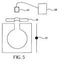
これら、インクジェットプリンタで使用される様々なコンポーネントの主要面を清掃、処理等するには、そのコンポーネントに対しマイクロプラズマ発生部材を近接配置又は一体化させてばよい。図5に、そのノズルプレート56の上方に電極54が配されたインクジェットプリントヘッド52の構成を示す。電極54の用途は、ヘッド52として例示したインクジェットプリンタコンポーネントの近くでマイクロプラズマを発生させることである。ここでいう“近く”とは、そのコンポーネントからの距離が1cm以内、という意味である。プリンタコンポーネントの近くで発生するマイクロプラズマには様々な用途がある。例えば、それを使用することで、そのコンポーネントの表面を初期的に清浄化するできるほか、そのコンポーネントの表面を修飾して疎水性、親水性、表面反応性等を向上させることができる。とりわけ重要なのは、発生させたマイクロプラズマを使用し乾燥物のこびりつき、例えば乾いたインクのこびりつき具合を管理することで、そのプリンタの始動及び停止シーケンスの信頼性、ひいてはそのプリンタの総合的な信頼性を高められることである。
In order to clean and process the main surfaces of various components used in these ink jet printers, a microplasma generating member may be disposed close to or integrated with the components. FIG. 5 shows a configuration of an
マイクロプラズマ、別称マイクロスケール放電は、電極(群)を介し外部電源からのエネルギが注入された個所に発生する。マイクロプラズマは気中放電の一種であり、所期方向(群)に沿った作用部位寸法が1mm未満になることを特徴としている。作用部位寸法とは、局所的な高輝度部位の寸法、局所的なイオン化部位の寸法、注目活性種の大半が集まっている部位の寸法(ある特定の中性活性種例えば単原子酸素の半値幅濃度での寸法)等、処理対象コンポーネントのうちマイクロプラズマが作用する部位の寸法のことである。マイクロプラズマの作用部位が局所的であり、インクジェットプリンタコンポーネントの表面積に比べ狭いことから判るように、コンポーネント処理時にはその作用部位を並進移動させた方がよい。即ち、マイクロプラズマ(群)による処理でその面の疎水性、親水性乃至表面反応性を高めるには、そのマイクロプラズマ(群)の作用部位をずらし又は作用面を切り替えることが有益である。マイクロプラズマ作用部位を、必要なら対応する電極及び電源と併せ並進移動させることで、処理するインクジェットプリンタコンポーネントを切り替えることもできる。 Microplasma, also known as microscale discharge, is generated at a location where energy from an external power source is injected through the electrode (s). Microplasma is a kind of air discharge, and is characterized in that the size of an action site along an intended direction (group) is less than 1 mm. The action site size is the size of the local high-intensity site, the size of the local ionization site, the size of the site where most of the active species of interest are gathered (the half-width of a specific neutral active species such as monatomic oxygen, etc. It is the dimension of the part where the microplasma acts among the components to be processed, such as the dimension in concentration). As can be seen from the fact that the active site of the microplasma is local and narrower than the surface area of the inkjet printer component, it is better to translate the active site during component processing. That is, in order to increase the hydrophobicity, hydrophilicity or surface reactivity of the surface by the treatment with the microplasma (group), it is beneficial to shift the working site of the microplasma (group) or switch the working surface. The inkjet printer component to be processed can also be switched by translating the microplasma working site, if necessary, along with the corresponding electrode and power source.
電極の種類としては、プラズマ発生所要個所にエネルギを注入するための電極のほか、それを補助する電極例えば基準電位提供用の電極がある。本願では、前者のことを主電極又は単に電極と呼び、後者のことを補助電極と呼んでいる。補助電極があると、主電極又は補助電極を正又は負にバイアスし、バイアスされた方の電極を陽極又は陰極とする二極放電を発生させることができる。電極の種類としては、更に、RFアンテナやマイクロ波導波路もある。例えば、RF誘導結合でプラズマを発生させる場合、アンテナを形成している導電トレースや導電ワイヤを電極として使用することができる。また、特許文献42に記載の開裂付リング共振器には、接地面と共に導波路を形成するリングに開裂(スプリット)が設けられている。この開裂即ち放電ギャップを挟み、一方の側にある導電トレース部分が主電極、他方の側にある導電トレース部分が補助電極としてそれぞれ機能する。
As the types of electrodes, there are an electrode for injecting energy into a place where plasma generation is required, and an electrode for assisting it, for example, an electrode for providing a reference potential. In the present application, the former is called a main electrode or simply an electrode, and the latter is called an auxiliary electrode. When there is an auxiliary electrode, it is possible to generate a bipolar discharge in which the main electrode or the auxiliary electrode is positively or negatively biased and the biased electrode is used as an anode or a cathode. Further, there are RF antennas and microwave waveguides as the types of electrodes. For example, when plasma is generated by RF inductive coupling, a conductive trace or a conductive wire forming an antenna can be used as an electrode. Further, in the ring resonator with a cleavage described in
電極54の駆動は、図5の如くその接続先の電源58で行うことができる。例えば、インクジェットプリントヘッド52のマニホルドを接地電位等の基準電位に固定した状態で、その電位と異なる電位が電極54に現れるよう電源58で電圧を印加する。その電圧は直流でも交流でも構わない。例えば、誘電体に絶縁は絵画生じないよう、周波数=Hz〜GHzオーダ、振幅=V〜kVオーダの範囲に属する任意周波数、任意振幅の交流電圧を使用する。逆に、電極54を所定の基準電位に固定し、それとは異なる電位がプリンタコンポーネント自体に現れるように電圧を印加してもよい。更には、主電極・補助電極間に電圧を印加する一方、インクジェットプリンタコンポーネントを電気的に絶縁してその電位をフロートさせる、といった構成も採りうる。
The
電極への印加電圧は、マイクロプラズマを初期発生させる際即ち点火の際には高くても構わないが、発生させたマイクロプラズマを維持していく段階では1kVを超えないようにすべきである。プリンタコンポーネントに物理的損傷が生じやすくなるからである。生じうる物理的損傷としては、誘電体が絶縁破壊するさいその表面に生じる焦げ目やクレータのように、見た目によくわかるタイプの損傷がある。そのコンポーネントの形成に低融点素材が使用されていれば、その素材の液化で目に付く損傷が生じることもある。更に、使用する電圧が高いと、そのコンポーネントに組み込まれている微細電子部品のうち静電荷に対し敏感なものが、静電荷蓄積によって損傷することが多くなる。従って、ウェブ処理の分野で既知の気中DBD処理、別称コロナ放電型ウェブ処理に倣い、そのピークトゥピーク値が5kVを上回る正弦波電圧をマイクロプラズマの点火及び維持に使用することは、可能だが望ましくないことである。 The voltage applied to the electrodes may be high when microplasma is initially generated, that is, during ignition, but should not exceed 1 kV in the stage of maintaining the generated microplasma. This is because physical damage is likely to occur in the printer component. Physical damage that can occur is a type of damage that is well visible, such as burns and craters that form on the surface of the dielectric when it breaks down. If a low melting point material is used to form the component, noticeable damage may occur due to the liquefaction of the material. Furthermore, when the voltage used is high, among the fine electronic components incorporated in the component, those sensitive to electrostatic charges are often damaged by electrostatic charge accumulation. Therefore, it is possible to use a sinusoidal voltage with a peak-to-peak value exceeding 5 kV to ignite and maintain a microplasma, following the air DBD processing known in the field of web processing, also known as corona discharge web processing. This is undesirable.
電極形成素材は、例えば、アルミニウム、タンタル、銀、金その他の金属を初めとする導電体や、ドープドシリコン、ドープドゲルマニウム、ドープドカーボン等のドープド半導体や、酸化インジウム錫、アルミニウムドープド酸化亜鉛等の透明高縮退半導体である。導電性ポリマ、ドープド半導体ポリマ、導電性ナノパーティクル分散系等も電極形成素材として使用することができる。更に、誘電体コーティングや誘電体内埋込で電極をパッシベートすること、例えばエポキシ系ポリマ、ポリイミド系ポリマ、酸化シリコン、酸窒化シリコン、窒化シリコン、五酸化タンタル、酸化アルミニウム等の有機物誘電体でコーティングすることもできる。加えて、金属、ドープド半導体等々の導電体を半導体コーティング又は半導体内埋込でパッシベートした構造の複合電極も使用することができる。半導体の電気的特性は導電体のそれと異なるので、複合電極の導電率は、コーティング等に使用した半導体の電気特性で決定づけられることとなる。 Electrode forming materials include, for example, conductors such as aluminum, tantalum, silver, gold and other metals, doped semiconductors such as doped silicon, doped germanium, and doped carbon, indium tin oxide, and aluminum doped oxide. It is a transparent highly degenerate semiconductor such as zinc. Conductive polymers, doped semiconductor polymers, conductive nanoparticle dispersions, and the like can also be used as electrode forming materials. Furthermore, the electrode is passivated by dielectric coating or embedded in the dielectric, for example, coated with an organic dielectric such as epoxy polymer, polyimide polymer, silicon oxide, silicon oxynitride, silicon nitride, tantalum pentoxide, aluminum oxide, etc. You can also. In addition, a composite electrode having a structure in which a conductor such as a metal or a doped semiconductor is passivated by semiconductor coating or embedded in a semiconductor can also be used. Since the electrical characteristics of the semiconductor are different from those of the conductor, the conductivity of the composite electrode is determined by the electrical characteristics of the semiconductor used for coating or the like.
電極位置、即ちプリンタコンポーネントの表面を処理するための電極の位置は処理対象コンポーネントの近くとする。ここでいう“近く”とは、そのコンポーネントからの距離が1cm以内、という意味である。コンポーネントからの距離が1cm以内であればよいので、その電極(群)は、そのコンポーネントと接触しないよう配してもよいし、そのコンポーネントと直に機械接触するよう配してもよいし、或いは微細加工、薄膜成長、積層等の処理でそのコンポーネント自体に形成してもよい。プリンタコンポーネント自体に形成等してそのコンポーネントに組み込んで得られる一体化電極、即ちコンポーネントと一体になっている電極を駆動する回路としては、コンポーネント外の回路を使用することも、そのコンポーネントに内蔵又は付設されている回路を使用することもできる。電極をコンポーネント上又はコンポーネント内に形成する手法としては、微細電子回路製造や微細電気機械システム(MEMS)製造の分野で既知の要領で能動回路素子や受動回路素子を形成する手法を使用することができる。電極(群)を一体化せず近くに配するだけにする場合は、その電極(群)を、外部回路で駆動する構成を採ることも、そのコンポーネントに内蔵又は付設されている回路で駆動する構成を採ることもできる。コンポーネント側の回路は、微細電子回路製造及びMEMS製造の分野で既知の手法に従い能動回路素子や受動回路素子を形成することで形成することができる。 The electrode position, that is, the position of the electrode for processing the surface of the printer component is close to the component to be processed. “Near” here means that the distance from the component is within 1 cm. Since the distance from the component may be within 1 cm, the electrode (s) may be arranged so as not to contact the component, or may be arranged so as to be in direct mechanical contact with the component, or You may form in the component itself by processes, such as microfabrication, thin film growth, and lamination | stacking. As a circuit for driving an integrated electrode obtained by being formed in the printer component itself or the like, that is, an electrode integrated with the component, a circuit outside the component can be used. An attached circuit can also be used. As a method of forming electrodes on or in a component, a method of forming active circuit elements and passive circuit elements in a manner known in the field of microelectronic circuit manufacturing or microelectromechanical system (MEMS) manufacturing may be used. it can. When the electrodes (groups) are simply arranged close to each other without being integrated, the electrodes (groups) may be driven by an external circuit, or may be driven by a circuit built in or attached to the component. A configuration can also be adopted. The component-side circuit can be formed by forming active circuit elements and passive circuit elements according to a known method in the fields of microelectronic circuit manufacturing and MEMS manufacturing.
電極使用個数は、発生させるマイクロプラズマの本数が1本なら最低1個でよい。マイクロプラズマ(群)を奇数個の電極で発生させるか偶数個の電極で発生させるかはその具体的な用途で異なってくる。主電極は個別型の電極でもよいし、複数個の電極からなる電極アレイでもでもよい。補助電極も個別型,電極アレイの両形態を採りうる。電極乃至そのアレイの形状を工夫することで、マイクロプラズマ発生動作及びマイクロプラズマ処理効果を処理対象コンポーネントの種類に相応しいものとすることができる。 The number of electrodes used may be at least one if the number of generated microplasmas is one. Whether the microplasma (group) is generated with an odd number of electrodes or an even number of electrodes depends on the specific application. The main electrode may be an individual electrode or an electrode array composed of a plurality of electrodes. Auxiliary electrodes can take both individual and electrode arrays. By devising the shape of the electrode or its array, the microplasma generation operation and the microplasma treatment effect can be made suitable for the type of component to be treated.
電極の形状・寸法は様々な形状・寸法にすることができる。例えば図5中の電極54をワイヤで実現する場合、そのワイヤを直線状にすることも、ループ、コイル等の二又は三次元形状にすることもできる。その場合、電極表面のうちマイクロプラズマが発生する空間に面する部分はワイヤ端的乃至凹凸的な性状になる。凹凸的な性状とは、その面の三次元的幾何形状に由来する特性、例えばピラミッド状の部分の先端、表面粗さとして現れる微視的凹凸等といった三次元的凹凸に由来する特性のことである。ご理解頂けるように、ここでいう“電極”にはより複雑なアセンブリも包含される。例えば、導電性コーティングが施された電気絶縁性のロッドの如く導電部分及び非導電部分を併有するアセンブリや、その周りにワイヤが捲回され又は金属等の導電体によるコーティングが施された電気絶縁性のチューブの如く中空部を有する電極である。
The shape and dimensions of the electrodes can be various shapes and dimensions. For example, when the
マイクロプラズマ処理を実行する環境は原則として大気圧下である。大気圧下ではあるが、特定種類の気体で気体流を発生させた方が、その処理環境を管理するのに都合がよい。使用する気体の組成はそのマイクロプラズマの用途に基づき決めるとよい。例えば、処理対象コンポーネント上にPECVDでコーティングを施したい場合、活性化すると凝縮性化学種を産生する物質を、プラズマ発生部位に送り込まれる気体に混ぜておけばよい。弗化ポリマ等からなる疎水層を成長させたい場合は、適当な弗素含有気体及び炭素含有気体を使用すると共に、マイクロプラズマで活性化された化学種を所望個所まで搬送することが可能な搬送気体を使用することで、そのインクジェットプリンタコンポーネント上に所要化学種を堆積させればよい。プラズマ成長やPECVDの分野で周知なものなら、他の種類の凝縮性素材でも同様に使用することができる。例えば、シラン、シロキサン等の気体を使用すれば、酸化シリコン、窒化シリコン又はシリコーン膜を成長させることができる。プラズマ発生部位に送り込まれる気体にアンモニア等の異種原子反応物を添加して特定の活性種を産生させることや、大気成分気体をプラズマ発生部位に送り込んで反応種を発生させることもできる。更に、インクジェットプリンタコンポーネントの表面から堆積物を除去したい場合は、プラズマで活性化してその堆積物に接触させると揮発種を産生することが知られている気体を、そのマイクロプラズマの近くまで導入すればよい。 The environment in which the microplasma treatment is performed is basically under atmospheric pressure. Although it is under atmospheric pressure, it is more convenient to manage the processing environment by generating a gas flow with a specific kind of gas. The composition of the gas to be used may be determined based on the use of the microplasma. For example, when it is desired to apply a coating by PECVD on a component to be processed, a substance that generates a condensable chemical species when activated can be mixed with a gas sent to a plasma generation site. When it is desired to grow a hydrophobic layer made of a fluorinated polymer, etc., an appropriate fluorine-containing gas and carbon-containing gas are used, and a carrier gas capable of transporting chemical species activated by microplasma to a desired location. The required chemical species may be deposited on the inkjet printer component. Other types of condensable materials can be used as well, as long as they are well known in the field of plasma growth and PECVD. For example, if a gas such as silane or siloxane is used, a silicon oxide, silicon nitride, or silicone film can be grown. It is also possible to add a heteroatom reactant such as ammonia to the gas sent to the plasma generation site to produce a specific active species, or to send an atmospheric component gas to the plasma generation site to generate a reactive species. In addition, if you want to remove deposits from the surface of an inkjet printer component, a gas known to produce volatile species when activated by plasma and contacted with the deposits is introduced close to the microplasma. That's fine.
ご理解頂けるように、搬送気体の役目は、マイクロプラズマで活性化させた化学種を所望の場所まで所要量届けることであるので、適切な搬送気体といえるのは、実質的に即ち十分長い距離区間及び期間に亘りその化学種と反応しないタイプの気体である。該当する気体としては、ヘリウム、ネオン、アルゴン等といった一般的な不活性ガス乃至希ガスのほかに、窒素(N2)ガス等の分子気体がある。搬送気体として使用する気体は、そのマイクロプラズマ処理の目的に応じて選定すればよい。更に、大気圧プラズマの分野で知られている通り、ヘリウム等の希ガスを使用すると、プラズマの点火及び維持に必要な印加電圧が低下する。重めの希ガス、例えばクリプトン、更にはキセノンを搬送気体に成分として添加すると、マイクロプラズマ発生部位で生じる輻射のスペクトラムが変化する。特に、キセノンが添加された気体をマイクロプラズマ発生部位に導入すると、そのマイクロプラズマに発する紫外線輻射が強まる。この紫外線輻射は、微生物による表面汚濁で生じる生体由来デブリを除去するプロセスで有用である。その紫外線輻射でオゾン等の酸化反応性中性種を発生させ、酸化的表面プロセスを増強することもできる。これらのことからご理解頂ける通り、処理対象インクジェットプリンタコンポーネントに及ぼしたい作用を踏まえ、プラズマ処理気体の成分を適切な成分にすることで、そのマイクロプラズマ処理で所望の如くにコンポーネントを清掃、アクティべート乃至パッシベートすることができる。プラズマ処理気体の成分を更に適切な成分にして、マイクロプラズマの動作及び安定性、更にはマイクロプラズマ処理の効率を高めることもできる。 As you can see, the role of the carrier gas is to deliver the required amount of chemical species activated by the microplasma to the desired location, so an appropriate carrier gas is essentially a sufficiently long distance. A type of gas that does not react with its chemical species over a period and period. Applicable gases include molecular gases such as nitrogen (N 2 ) gas in addition to general inert gases or rare gases such as helium, neon, and argon. What is necessary is just to select the gas used as carrier gas according to the objective of the microplasma process. Furthermore, as is known in the field of atmospheric pressure plasma, the use of a noble gas such as helium reduces the applied voltage required to ignite and maintain the plasma. When a heavier noble gas such as krypton or further xenon is added as a component to the carrier gas, the spectrum of radiation generated at the microplasma generation site changes. In particular, when a gas to which xenon is added is introduced into a microplasma generation site, ultraviolet radiation emitted from the microplasma is increased. This ultraviolet radiation is useful in the process of removing biological debris generated by surface contamination by microorganisms. The ultraviolet radiation can generate oxidative reactive neutral species such as ozone to enhance the oxidative surface process. As you can see from this, based on the effects that you want to affect the inkjet printer component to be processed, the components of the plasma processing gas are changed to the appropriate components so that the microplasma processing can clean and activate the components as desired. Or passivated. It is also possible to increase the operation and stability of the microplasma and further improve the efficiency of the microplasma processing by making the plasma processing gas component a more appropriate component.
但し、使用する気体の成分がどのような成分でも、大気圧付近の圧力下でマイクロプラズマ処理プロセスを進行させることは有益なことである。ここでいう“大気圧付近”とは400〜1100Torr域内にある圧力のことである。特に560〜960Torr域内の圧力が望ましい。この域内の高めの圧力値で処理プロセスを進行させたければ、処理対象コンポーネントの近くに処理気体を導入するためのマニホルド等、通常の印刷プロセスで空気流又はインク流の発生に使用されるマニホルドで圧力を高めればよい。逆に、大気又は外部気体源からプラズマ発生部位に供給されている処理気体をそのマニホルドで吸引して排出させれば、その部位内を低めの圧力値にすることができる。 However, it is beneficial to advance the microplasma treatment process under a pressure near atmospheric pressure, regardless of the gas component used. Here, “near atmospheric pressure” means a pressure within a range of 400 to 1100 Torr. In particular, a pressure in the range of 560 to 960 Torr is desirable. If you want the process to proceed at higher pressure values in this area, use a manifold that is used to generate air or ink flow in the normal printing process, such as a manifold to introduce process gas near the component being processed. What is necessary is just to raise a pressure. Conversely, if the processing gas supplied from the atmosphere or an external gas source to the plasma generation site is sucked and discharged by the manifold, the pressure in the site can be lowered.
そして、図5に示した構成では、インクジェットプリンタコンポーネント及び電極の周囲で気体流を発生させることができる。例えば、気体を大気圧中で任意方向から電極周辺に流すことで、そのコンポーネント及び電極の周囲に気体流を発生させることができる。また、そのコンポーネントの内部を大気圧より低い圧力や高い圧力にすることもできる。例えば、インクジェットプリントヘッドのマニホルドボア内を大気圧より低い圧力にすると、ノズルボア経由でそのヘッド内に気体が引き込まれてくる。逆に、そのマニホルド内を大気圧より高い圧力にすると、ノズルボア経由でヘッド・電極間空間に気体が吐き出されてくる。こうした電極付近での気体流管理は、電極付近のマイクロプラズマに近いところでの気体の組成及び流れを保つのに役立つ。これもまたご理解頂ける通り、マイクロプラズマの近く、即ちそのマイクロプラズマの近辺、周囲又は内部における気体流を管理することで、そのプラズマで産生される気相の反応種を所望の場所に運ぶ手段を提供することができる。 In the configuration shown in FIG. 5, a gas flow can be generated around the inkjet printer component and the electrode. For example, a gas flow can be generated around the component and the electrode by flowing the gas around the electrode from an arbitrary direction at atmospheric pressure. Further, the interior of the component can be set to a pressure lower than or higher than the atmospheric pressure. For example, if the pressure in the manifold bore of the ink jet print head is made lower than atmospheric pressure, gas is drawn into the head via the nozzle bore. On the contrary, when the pressure in the manifold is higher than the atmospheric pressure, gas is discharged into the head-electrode space via the nozzle bore. Such gas flow management near the electrodes helps to maintain the gas composition and flow near the microplasma near the electrodes. As can also be seen, by managing the gas flow near the microplasma, i.e., near, around, or within the microplasma, a means to bring the gas phase reactive species produced by the plasma to the desired location. Can be provided.
図6に、インクジェットプリンタコンポーネントたるガターの上方に電極64を配した例を示す。このガターは図2に示したものと同様であり、電極64はその流体回収面66から見て上方に配されている。電極64の役目はガターの近く、即ちガターから1cm以内の場所でマイクロプラズマを発生させることである。ガターに限らず、インクジェットプリンタコンポーネントの近くでマイクロプラズマを発生させることは、多くの点で有益なことである。例えば、そのコンポーネントの表面を初期的に清浄化することができる。そのコンポーネントの表面を修飾して疎水性、親水性、表面反応性等を高めることができる。プリンタ使用に伴う表面汚損乃至表面特性劣化を妨げること、例えば弗化炭化水素かシリコンの酸化物、炭化物乃至窒化物を流体回収面上に堆積させてその濡れ性を調整することもできる。特に重要なことに、インク等の流体に含まれる成分が乾燥してガターの流体回収面にこびりつき、その面の機能ひいてはガター全体の動作に障りとなることを、マイクロプラズマの発生で規制することができる。
FIG. 6 shows an example in which an
このように、ガター表面の諸部位に対しマイクロプラズマによる清掃、修飾等を施しその面の主立った特性を管理することで、そのインクジェットプリンタの始動/停止シーケンスひいてはプリンタ動作全体の信頼性を高めることができる。また、そのガターの流体回収面、流体回収チャネル壁等、ガター構成要素を電極として使用する構成を採れることもご理解頂けよう。更に、先の説明から自明な通り、ガター内部の流体回収チャネル68をその手段として利用し、マイクロプラズマの近くに気体流を供給することで、そのマイクロプラズマの安定性を所望水準まで高めることや、そのマイクロプラズマから所望の化学的乃至物理的効果が得られるようにすることができる。
In this way, by cleaning and modifying the parts of the gutter surface with microplasma and managing the main characteristics of the surface, the start / stop sequence of the ink jet printer and thus the reliability of the entire printer operation are improved. Can do. It will also be appreciated that the gutter components, such as the fluid recovery surface of the gutter and the fluid recovery channel wall, can be configured as electrodes. Further, as is obvious from the above description, by using the
図7に、インクジェットプリンタコンポーネントの上方に配される個別型電極の別例76を示す。この電極76は、マニホルド72上にノズルプレート74を装着した構成を有するインクジェットプリントヘッドの上方に配されており、立体的な開裂付筒状共振電極76及びそれに固定された平板コネクタ77で構成されている。具体的には、導電性を有する外郭シリンダの内側に中空部分又は固体誘電体充填部分を挟み接地シリンダを同心配置した構成の共振電極76と共に、接地プレートを中空部分又は固体誘電体充填部分で覆い更にそれを導電性のある外郭層で覆った構成のコネクタ77を使用し、接地面が形成されるよう電極76内の接地シリンダをコネクタ77内の接地プレートに接続した構成である。逆に、接地シリンダを共振電極の外側に同心配置する一方、接地プレートを平板コネクタの外面に配して接地シリンダと接続することでも、接地面を形成することができる。
FIG. 7 shows another example 76 of the individual electrode disposed above the inkjet printer component. The
更に、円筒断面でない電極を共振電極76として用いることや、平板状でないコネクタをコネクタ77として用いることも可能である。電極76及びコネクタ77の導電部分は、対応する接地面と共に、電磁波をギャップ78に導く導波路として機能する。開裂筒状共振電極76のギャップ78における電磁波の位相は、その電磁波の周波数がその電極76の共振周波数と同周波数である場合、そのギャップ78を挟み180°異なる位相になる。電極76が中空であれば、更に、電極76の内側を介しそのギャップ78に気体流を供給することで、大気圧マイクロプラズマを制御環境下で発生させることができる。開裂付筒状共振電極の長所は、発生するマイクロプラズマの寸法をある方向に沿って長尺にすることができ、従ってインクジェットプリンタコンポーネント上の複数個所を同時に処理することができることである。開裂付筒状共振電極の動作周波数は筒状部分の寸法で決まるので、kHzオーダからGHzオーダまで様々な周波数にすることができる。
Furthermore, an electrode having a non-cylindrical cross section can be used as the
図8に、インクジェットプリンタコンポーネントの上方に配される個別型電極の別例82を示す。この電極82は、マニホルド88及びそれに装着されたノズルプレート86を有するインクジェットプリントヘッドの上方に配されており、コーティング84によって被覆されている。電極82を覆うコーティング84の厚みは例えば10nm〜10μm程度、素材は例えば金属質、半導体又は絶縁体である。金属質コーティングにはタンタル、プラチナ等の耐腐食性素材が、半導体コーティングにはシリコンカーバイド又は導電性酸化物が、絶縁性コーティングにはテフロン(登録商標)、ガラス状二酸化シリコン、酸化シリコン、酸化アルミニウム等の誘電体が適している。複数種類の物質を組み合わせた複合素材、即ちその化学的性質が異なる複数の成分又は部分を有する素材を、コーティング素材として使用することもできる。いずれにせよ、こうしたコーティング84には幾つかのメリットがある。例えば、電極82をコーティング84で覆うことで、マイクロプラズマ中で産生される強力な反応種に対し電極形成素材を化学的にパッシベートすることができる。また、イオン衝撃による二次電子放射の係数等、電極82の二次放射特性を調整することもできる。電極82の電位は接地電位に対し同電位でも異電位でもよい。電極82の駆動電圧は直流でも交流でもよい。交流電圧を使用する場合、先に図5を参照して説明した通り、1V〜50KVの振幅域内、1Hz〜100GHzの周波数域内ならどのような値でも使用することができる。但し、10kHz〜10GHz域内の周波数の方がよい。
FIG. 8 shows another example 82 of individual electrodes disposed above an inkjet printer component. The
図9に、インクジェットプリンタコンポーネントの上方に複数個の電極92,94を配した例を示す。電極92,94はノズルプレート96、ノズルボア99及びマニホルド98を有するインクジェットプリントヘッドの上方に配されており、その個数が複数である点を除けば図5に示したものと同様の構成である。電極92,94を電気的に駆動するには、多々ある手段のうちいずれかでそれらに電圧を印加すればよい。電極92,94に対するこの電圧印加によって、コンポーネントたるヘッドの近くでマイクロプラズマ(群)を発生させることができる。電極92,94への印加電圧は直流でも交流でも構わない。交流電圧ならば1Hz〜100GHzの周波数域内、1V〜50kVの振幅域内の電圧を使用するとよい。こうした限界は誘電体の絶縁破壊との関連で決まってくる。更に、電気回路上、インクジェットプリンタコンポーネントは基準電位例えば接地電位に固定しておくことも電気的にフロートさせておくことも可能であるので、例えば、電極94を基準電位例えば接地電位に固定した状態で電極92を電気的に駆動することができる。また、電圧印加の仕方次第で、マイクロプラズマ発生個所が電極92・電極94間になることもあれば電極92,94・プレート96間になることもある。例えば、電極92・94間に電圧を印加すると、それらで挟まれているギャップ領域でマイクロプラズマが発生し、そのマイクロプラズマ内で化学種が産生される。その化学種がインクジェットプリンタコンポーネントの近くまで辿り着かなければ、そのコンポーネントに所期の表面処理が施されることはない。そのため、それら電極92,94の個々の対は、コンポーネント側にある特徴的部位群、例えばプレート96上の個々のボア99の上方でマイクロプラズマ(群)が生じるよう、ひいてはそのマイクロプラズマ(群)で諸特徴部位が処理されることとなるよう配置される。そのコンポーネントに印加される基準電位が適切であれば、電極92・94間方向に沿ったマイクロプラズマの寸法を1mm未満に抑えつつ、マイクロプラズマ作用部位をコンポーネント表面沿いに拡げることができる。マイクロプラズマ作用部位を一次元的又は二次元的に拡げることで、大気圧マイクロプラズマ処理の効果例えば清掃、表面成長、表面反応性増強等の効果を強めることができる。また、インクジェットプリンタコンポーネント側にある特徴部位と電極の間に1対1の対応関係が生じるよう、複数個の電極を配置することもできる。その種の構成では、複数個の電極を同時並行的に駆動することも、そのインクジェットプリンタコンポーネントとは独立に駆動することもできる。そのいずれでも、個々の電極にて局所的なマイクロプラズマを発生させることができる。更に、そのコンポーネントの導電部分を補助電極として機能させることもできる。
FIG. 9 shows an example in which a plurality of
図10aに、複数個の個別型電極102,104をそれぞれ誘電体101に埋め込みインクジェットプリンタコンポーネントの上方に配した例を示す。また、図10bに、複数個の電極108を同じ誘電体101に埋め込みインクジェットプリンタコンポーネントの上方に配した例を示す。これらの図におけるコンポーネントはノズルプレート106を有するインクジェットプリントヘッドである。また、ここでいう“埋込”とは、その電極の外表面をほぼ全体に亘り固相又は液相の物質で覆うことである。
FIG. 10a shows an example in which a plurality of
電極を誘電体101に埋め込むのは、マイクロプラズマで産生される化学種のうち腐食性を有するものからその電極を保護して破損を防ぐためである。電極が埋め込まれる誘電体101の電気抵抗値は例えば105Ω・cm超とし、その厚みはマイクロプラズマ発生に支障とならない任意値とする。誘電体素材の絶縁破壊特性、稼働電圧及び電極製造方法に従い決めればよい。その電気抵抗値が105Ω・cm超の誘電体101を形成可能な素材は数多くあり、例えばテフロン(登録商標)、エポキシ、シリコーン樹脂、ポリイミド等のように反応性が低く熱安定性が高い有機ポリマを使用できるほか、炭素を含有する複合素材も使用することができる。ここでいう複合素材とは、その化学的組成が異なる複数個の部位を有する固体のことである。その例としては、ガラス繊維入りのエポキシ、ガラス繊維で強化されたガラス入りテフロン(登録商標)ポリマ等がある。ご理解頂けるように、本発明の実施に際しては、これ以外の様々な複合素材も使用することができる。誘電体101の素材としては、更に、種々の絶縁性無機素材も使用することができる。例えば、マグネシウム、硼素、シリコン、アルミニウム、チタン、タンタル、ニオブ、ハフニウム、クロム、ジルコン等の金属の酸化物、窒化物、酸窒化物、硫化物、金属含有酸化物誘導体等である。二成分素材でも三成分以上の多成分素材でも構わない。金属含有酸化物誘導体とは、その金属を少なくとも20原子%含有する酸化物ベースの誘電体化合物のことである。例えば、酸化セリウムを20%を含有する酸化ジルコン化合物は、酸化ジルコン誘導体の一種であると同時に酸化セリウム誘導体の一種でもある。 The reason why the electrode is embedded in the dielectric 101 is to protect the electrode from corrosive chemical species produced by microplasma and prevent damage. The electric resistance value of the dielectric 101 in which the electrode is embedded is, for example, more than 10 5 Ω · cm, and the thickness thereof is an arbitrary value that does not hinder the generation of microplasma. What is necessary is just to determine according to the dielectric breakdown characteristic of a dielectric material, an operating voltage, and an electrode manufacturing method. There are many materials that can form the dielectric 101 having an electrical resistance value exceeding 10 5 Ω · cm. For example, Teflon (registered trademark), epoxy, silicone resin, polyimide, etc. have low reactivity and high thermal stability. Organic polymers can be used, and composite materials containing carbon can also be used. The composite material here is a solid having a plurality of sites having different chemical compositions. Examples thereof include glass-filled epoxy, glass-filled Teflon (registered trademark) polymer reinforced with glass fiber, and the like. As can be appreciated, various other composite materials can be used in the practice of the present invention. As the material of the dielectric 101, various insulating inorganic materials can also be used. Examples thereof include oxides, nitrides, oxynitrides, sulfides, metal-containing oxide derivatives of metals such as magnesium, boron, silicon, aluminum, titanium, tantalum, niobium, hafnium, chromium, and zircon. A two-component material or a multi-component material having three or more components may be used. A metal-containing oxide derivative is an oxide-based dielectric compound containing at least 20 atomic% of the metal. For example, a zircon oxide compound containing 20% cerium oxide is not only a kind of zircon oxide derivative but also a kind of cerium oxide derivative.
また、こうした誘電体の素材は、結晶質、ガラス質、非晶質のいずれであってもよい。誘電体分野でいわゆる当業者にとり既知の如く、埋込先誘電体となりうる素材はほかにも数多くあり、本発明ではそうした誘電体も使用することができる。また、その埋込先誘電体の表面は、凹凸のないスムースな面にすることも凹凸模様のある面にすることも可能である。本発明の実施に当たっては、そうした凹凸模様のある構成を採ることができ、また様々な凹凸模様付与手法を採ることができる。更に、使用する電極の個数が複数個の場合でも、先に図9を参照して説明した様々な構成で駆動することができ、それによってインクジェットプリンタコンポーネントの近くでマイクロプラズマを発生させることができる。 Such a dielectric material may be crystalline, glassy, or amorphous. As known to those skilled in the art in the dielectric field, there are many other materials that can be embedded dielectrics, and such dielectrics can also be used in the present invention. In addition, the surface of the embedded dielectric can be a smooth surface without unevenness or a surface with unevenness. In carrying out the present invention, it is possible to adopt a configuration having such a concavo-convex pattern, and it is possible to employ various concavo-convex pattern imparting techniques. Furthermore, even when a plurality of electrodes are used, they can be driven with various configurations described above with reference to FIG. 9, thereby generating a microplasma near the inkjet printer component. .
図11に、インクジェットプリンタコンポーネントの上方に長尺電極110を配した例を示す。この電極110は、ノズルプレート112、ノズルボア114及びマニホルド116を有するインクジェットプリントヘッドの上方に至近配置されており、そのアスペクト比が10を上回る長尺電極となっている。アスペクト比とは他の一又は二方向の寸法に対する長手方向寸法の比のことであり、長手方向寸法とは対応するヘッドの一表面乃至多表面に対しほぼ平行な面に沿った寸法のことである。図示例の電極110は長方形断面であるが、本発明は他形状の長尺電極でも実施することができる。例えば、プリズムに類似した三角形断面の長尺電極や、対応するコンポーネントの一表面乃至多表面に対しほぼ平行な面に沿った長さをその直径で除した値が10を上回る細長いワイヤ等、様々な幾何学的構成のものを使用することができる。また、図示例の電極110を電気的に駆動し対応するコンポーネントの近くでマイクロプラズマを発生させる手法としては、図5を参照して説明したものを使用することができる。更に、図5を参照して説明した通り、電極110の周囲で気体流を発生させ、そのコンポーネント自体を利用してコンポーネント及びマイクロプラズマ作用域の近くまで気体流を供給する、という手法も使用することができる。
FIG. 11 shows an example in which a
図12に、インクジェットプリンタコンポーネントの上方に長尺電極120を配した例を示す。この例では、図11のそれと同様に長尺な電極120が、ノズルプレート124、ノズルボア126及びマニホルド128を有するコンポーネントの近くに配置されている。更に、その電極120は、図8の如きコーティングや図10a及び図10bの如き埋込で形成された誘電体層122を有している。本発明は、このように、様々な形態で他の素材でコーティングされ又は他の素材に埋め込まれた長尺電極を使用し実施することができる。本発明は、更に、長尺電極やそれを他の素材でコーティングし又は他の素材に埋め込んだものを複数本使用する形態でも実施することができる。例えば、対をなす長尺電極間のギャップでマイクロプラズマが発生するよう、またその発生個所がインクジェットコンポーネントの近くになるよう、一対又は複数対の長尺電極を配置及び個別駆動する形態である。
FIG. 12 shows an example in which a
図13a、図13b及び図13cに、それぞれ、主電極又は補助電極として使用される複数個の電極をインクジェットプリンタコンポーネント、具体的にはインクジェットプリントヘッドと一体化した例を示す。ここでいう一体化とは、本体から分離することができないように個々の部分を形成又は配置することである。例えば、これらの図のインクジェットプリントヘッドでは、ノズルボア134及びマニホルド136の近くに配置されるノズルプレート132に複数個の電極130が一体化されている。図8、図10a、図10b及び図12を参照して説明した通り、誘電体で覆い又は誘電体に埋め込むことで、この一体化電極130はパッシベートすることができる。
FIG. 13a, FIG. 13b and FIG. 13c show examples in which a plurality of electrodes used as main electrodes or auxiliary electrodes are integrated with an ink jet printer component, specifically, an ink jet print head. The term “integration” as used herein refers to forming or arranging individual portions so that they cannot be separated from the main body. For example, in the ink jet print head shown in these drawings, a plurality of
図13a、図13b及び図13cには、更に、幾種類かの駆動回路138が例示されている。この回路138は、インクジェットプリンタコンポーネントの近くでマイクロプラズマが発生するよう、電極130を駆動するための回路である。ご理解頂ける通り、本発明の実施に当たっては、これ以外の構成の電極や駆動回路も使用することができる。例えば、図13aに示す例や図13bに示す例では、ノズルプレート132に一体化されている複数個の電極130を、外付けの駆動回路138例えば電源によって電気的に駆動している。ご承知の通り大電力回路の小型化が進んできているので、電源全体をコンポーネント例えばインクジェットプリントヘッドと一体化させた形態にて、本発明を実施することも可能である。また、本発明を実施するに当たっては、図5、図7及び図9を参照して説明したものを含め、様々な構成の電気回路を電極130の駆動に使用することができる。例えば図13aでは、主電極及び補助電極が駆動回路138により互いに逆相で駆動されている。
In FIGS. 13a, 13b and 13c, several types of
次に、図13bでは、特許文献43及び42(Hopwood et al.)に記載のRFアンテナ又はマイクロ波導波路が形成されるよう複数個の電極130が配置され、それらの電極130が外部電位を基準にして駆動されている。具体的には、RFアンテナ電極130から輻射されるRF電力の集中個所又はマイクロ波導波路電極130同士の狭間部分がノズルボア134の近くに位置することとなるよう、それらの電極130が配置されている。また、外部電位を基準にするのではなく、補助電極の電位を基準にして電極130を駆動することもできる。補助電極としては、図中のマニホルド136等、インクジェットプリンタコンポーネントの他部分を使用してもよいし、図示しないが別途電極を設けて使用してもよい。
Next, in FIG. 13b, a plurality of
そして、図13cでは、主電極又は補助電極となる複数個の電極130がインクジェットプリンタコンポーネントたるインクジェットプリントヘッドに一体化されている。それら一体化電極130のうちあるものは駆動対象となる電極であり、他のあるものは端子139経由で基準電位Vrefに固定される電極である。図示例では、前者と後者とが交互に位置することとなるよう、奇数個又は偶数個の電極130が配されている。また、電極130のうち端子139に接続されているものの電位は、端子139を接地することで接地電位にすることができるほか、基準電位Vrefを変調することで操作することができる。その操作手法としては、プラズマ発生の分野でいわゆる当業者に知られている手法を使用することができる。但し、それらの電極130の構成、例えばその主電極及び補助電極の個数及び寸法比や誘電体の存否等と違背しないようにすべきである。
In FIG. 13c, a plurality of
図14に、複数本の長尺電極140をインクジェットプリンタコンポーネントに一体化した例を示す。この例では、図11又は図12に示したものと同じく長尺な電極140が、ノズルボア144及びマニホルド146の近くにあるノズルプレート142に一体化され、駆動回路148によって電気的に駆動されている。ご理解頂けるように、図11及び図12を参照して説明した例と同じく、この例でも、長尺電極140を駆動しコンポーネントの近くでマイクロプラズマ(群)を発生させる手段として様々な手段を使用することができる。また、それら複数個の一体化長尺電極140だけでなく、マイクロプラズマを制御、生成及び維持するための電気回路も、そのコンポーネント例えばインクジェットプリントヘッドに一体化させることができる。
FIG. 14 shows an example in which a plurality of long electrodes 140 are integrated into an inkjet printer component. In this example, a long electrode 140 similar to that shown in FIG. 11 or 12 is integrated into the
図15a及び図15bに、ノズルプレート154上に形成されているノズルボア152の近くに導電シールド150を配した例を示す。プレート154はマニホルド156と共にインクジェットプリンタコンポーネントたるインクジェットプリントヘッドを形成しており、図15aの例ではそのヘッドとシールド150が一体、図15bの例では別体になっている。そのシールド150は導電層として形成されており、対応するヘッドとマイクロプラズマ等の電気的雑音源との間に位置している。こうしたシールド150をインクジェットプリンタコンポーネントに付設することで、そのコンポーネントの動作上の信頼性を高めることができる。
15a and 15b show an example in which the
こうした導電シールドを形成する素材としては、その抵抗値が100Ω・cmを下回る様々な導電体を使用することができる。例えば、銅、アルミニウム、タンタル、金、銀、ニオブ、チタン等の金属や、それらの金属の合金や、スチール等を使用するのが望ましい。導電性透明酸化物等の透明導電体も導電シールド形成素材として使用可能である。導電シールド形成素材としては、更に、ポリチオフェンベース素材等の導電性ポリマや、カーボンナノチューブ等のカーボンベース素材を含む導電性分散系や、導電素材を含むナノパーティクル分散系も使用することができる。 As a material for forming such a conductive shield, various conductors having a resistance value lower than 100 Ω · cm can be used. For example, it is desirable to use metals such as copper, aluminum, tantalum, gold, silver, niobium, titanium, alloys of these metals, steel, and the like. A transparent conductor such as a conductive transparent oxide can also be used as a conductive shield forming material. Further, as the conductive shield forming material, a conductive polymer such as a polythiophene base material, a conductive dispersion system including a carbon base material such as a carbon nanotube, and a nanoparticle dispersion system including a conductive material can also be used.
特に、導電シールドをインクジェットプリンタコンポーネントに一体化すると、そのコンポーネントの動作上の信頼性が更に向上する。これは、マイクロプラズマを発生させる際に、そのインクジェットプリンタコンポーネントの通常時稼働電圧より高い電圧を印加しなければならなかったり、通常時稼働電流より大きな局所的電流が生じたりしても、導電シールドが一体化になっていれば、損傷しきい値超の電圧乃至電流等、通常時稼働条件より厳しい条件に起因するコンポーネント損傷をかなりの程度避けうるからである。いずれにせよ、インクジェットプリンタコンポーネントとマイクロプラズマ等の電気的雑音源との間に導電シールドを差し挟むことで、その種のコンポーネントでよく使用される電気回路、例えばCMOS回路等の電気回路乃至微細電子回路のように繊細なものを含む種々の電気回路を、ほぼ全て、その雑音源に発する電気的雑音から効果的に保護することができる。 In particular, the integration of the conductive shield into the inkjet printer component further improves the operational reliability of the component. This is because when a microplasma is generated, a conductive shield is applied even if a voltage higher than the normal operating voltage of the inkjet printer component must be applied or a local current larger than the normal operating current is generated. This is because component damage caused by severer conditions than normal operating conditions such as voltage or current exceeding the damage threshold can be avoided to a considerable extent. In any case, by interposing a conductive shield between an inkjet printer component and an electrical noise source such as microplasma, an electrical circuit often used in such components, for example, an electrical circuit such as a CMOS circuit or a fine electron Almost all of the various electrical circuits, including circuit sensitive ones, can be effectively protected from the electrical noise emitted by the noise source.
導電シールド150は、その接続抵抗値が10Ω未満となるよう接地等の基準電位源に導通接続することができる。その接続に使用できる手法も幾つか知られている。しかし、シールド150をあらゆる基準電位源から切り離し、電気的雑音源の電位に従動させるようにした方がよい場合もある。この手法のことを、本件技術分野では電圧フロートと呼んでいる。例えば、接地されておらず電圧フロートしている電気回路をプラズマに曝すと、その回路の電位はフロート電位となる。フロート電位とは、プラズマに対するフロート接触でそのプラズマから取得する電荷量が差し引き0となる電位のことである。こうした場合、もしシールド150を接地してしまうと、シールド150との間に生じる大きな電位差が原因でその回路が損傷してしまうことがある。従って、そうした繊細な回路がマイクロプラズマ等の電気的雑音源に対し曝露される場合は、シールド150を電圧フロートさせるべきである。これは、接地されている物体とプラズマとの間の電位差に比べ、電圧フロートしている物体とプラズマとの間の電位差は顕著に小さく、従ってその物体に射突してくるイオンのエネルギがかなり小さくなるからである。特に、容量結合性交流放電の場合、印加電圧の半周期中に、プラズマ電位が数百Vもの高電圧まで上昇していく。そうした場合でも、シールド150及びそれにより遮蔽されるべき回路を電圧フロートさせることで、プラズマとシールド150乃至回路との間の電位差を、プラズマ電位とフロート電位の差に等しい値に保つことができる。その値は通常は10Vオーダである。
The
更に、マイクロプラズマの用途によっては、マイクロプラズマ・インクジェットプリンタコンポーネント間に介在する導電シールドだけでなく、そのコンポーネント自体も電圧フロートさせた方がよい場合がある。電圧フロートしている導電シールドの方がマイクロプラズマに近いので、イオンがそのシールドの表面に射突しそこでエネルギが吸収されることになるからである。即ち、イオンのエネルギのうち、並進運動に係る運動エネルギの形態をとらないもの、例えばそのイオン種に係るイオン化ポテンシャルの形態をとるものを、イオン射突先シールド面で吸収させることができる。また、導電シールドの配設やインクジェットプリンタコンポーネントとの一体化は、本来、そのコンポーネントの動作上の信頼性を向上させることを目的としたものであるが、ご理解頂けるようにそれ以外の機能を導電シールドに担わせることもできる。例えば、何らかの電気回路を使用して電極を駆動しコンポーネントの近くでマイクロプラズマを発生させる場合、コンポーネント上の繊細部分を保護して動作上の信頼性を向上させるという本来の機能に加え、補助電極としての機能も担わせることができる。 Furthermore, depending on the application of the microplasma, not only the conductive shield interposed between the microplasma and ink jet printer components, but also the components themselves may be voltage floated. This is because the voltage-floating conductive shield is closer to microplasma, so that ions strike the surface of the shield and energy is absorbed there. In other words, the ion energy that does not take the form of the kinetic energy related to the translational movement, for example, the form that takes the form of the ionization potential related to the ion species, can be absorbed by the ion projection tip shield surface. In addition, the installation of conductive shields and integration with inkjet printer components are originally intended to improve the operational reliability of the components, but other functions are provided so that you can understand them. It can also be carried by a conductive shield. For example, when driving an electrode using some electrical circuit to generate a microplasma near the component, in addition to the original function of protecting delicate parts on the component and improving operational reliability, the auxiliary electrode It can also serve as a function.
図16に、複数個ある電極162と導電シールド164の間に誘電体層160を差し挟んだ例を示す。この例では、それら電極162、誘電体層160及びシールド164が、ノズルプレート166上にある1個又は複数個のノズルボア168の近くに位置することとなるようノズルプレート166と一体化されている。そのノズルプレート166は、マニホルド169と共に、インクジェットプリンタコンポーネントたるインクジェットプリントヘッドを構成している。このように誘電体層を一体化させると電極群が導電シールドから電気的に絶縁されるため、導電シールドに導通させないようにしつつそれらの電極に電圧を印加すること、ひいてはインクジェットプリンタコンポーネントの近くでマイクロプラズマを発生させることができる。なお、導電シールドとしては、金、銅、アルミニウム、タンタル等、導電性のある金属で形成されているものや、シリコン、ポリシリコン等に燐、硼素等をドーピングした高ドープド半導体で形成されているものや、例えば導電性のあるドープドシリコンカーバイドで形成されているものや、例えば導電性のあるドープドダイアモンド様カーボンで形成されているものを、好適に使用することができる。酸化インジウム錫、弗素ドープド酸化錫、アルミニウムドープド酸化亜鉛等、導電性のある酸化物も使用することができる。
FIG. 16 shows an example in which a
図15を参照して説明した通り、この導電シールドは、接地等の基準電位源に接続することができるほか、あらゆる基準電位源から切り離して電圧フロートさせ、周囲の電気的雑音源によって誘起される電位を取得する構成にすることができる。また、インクジェットプリンタコンポーネントに一体化させた複数個の電極を電気的に駆動しマイクロプラズマを発生させる手段、それらの電極を電気的に駆動する回路、それらの電極の寸法及び形状等々は、本発明の実施に当たり、プラズマ生成の分野で既知のあらゆる手段乃至回路構成としまた様々な寸法及び形状にすることができる。 As described with reference to FIG. 15, this conductive shield can be connected to a reference potential source such as ground, and can be disconnected from any reference potential source and floated, and induced by an ambient electrical noise source. It can be configured to acquire a potential. Further, means for electrically driving a plurality of electrodes integrated with an inkjet printer component to generate microplasma, a circuit for electrically driving these electrodes, dimensions and shapes of these electrodes, etc. In practice, any means or circuit configuration known in the field of plasma generation can be used and can be of various sizes and shapes.
インクジェットプリンタコンポーネントに複数個の電極を一体化させるに当たっては、その電極を裸で使用することも、前述の如く様々な素材でコーティングし又はそれに埋め込むことも、或いは一方向以上の方向に沿って長尺な形状にすることもできる。また、ご理解頂けるように、図16に示した一体化電極に対する気体流の供給も、図5を参照して先に説明したものと同様の手法で行うことができる。例えば、図16に示した構成では、誘電体層160上にある一体化電極162の近くでマイクロプラズマが発生する。マニホルド169内を大気圧より高い圧力又は低い圧力に保つことで、そのマイクロプラズマの近くを流れる気体に影響を及ぼすことができる。
When integrating a plurality of electrodes into an inkjet printer component, the electrodes can be used bare, coated with various materials as described above, embedded in them, or long along one or more directions. It can also be made into a scale shape. Further, as can be understood, the gas flow can be supplied to the integrated electrode shown in FIG. 16 by the same method as described above with reference to FIG. For example, in the configuration shown in FIG. 16, microplasma is generated near the
図17に、複数個ある長尺電極170とノズルプレート172の間に誘電体層178及び導電シールド179を差し挟んだ別例を示す。この構成では、ノズルボア174ののうち1個又は複数の近くに位置することとなるよう、それらの長尺電極170がノズルプレート172の表面に一体化され、またそのプレート172がマニホルド176に固定されている。
FIG. 17 shows another example in which a
この図の構成では、インクジェットプリンタコンポーネントに一体化されている長尺電極170のうち幾つかが主電極、主電極間に位置している残りの長尺電極が補助電極として使用されている。図示例では、更に、電極170と電極170とで挟まれた空間内にノズルプレート172上のノズルボア174が位置するよう、それらの電極170が配置されている。この図には、また、電極170を駆動しコンポーネントの近くでマイクロプラズマを発生させる回路の構成も例示されている。ご理解頂けるように、電極駆動用の電気回路は、前述の如く導電シールドを利用する構成を含め、様々な構成にすることができる。
In the configuration of this figure, some of the
図18aに、ある方向に沿って各複数個の導電層180及び誘電体層182を交互配列した電極アセンブリの例を示す。図示例では、導電層180及び誘電体層182の配列方向が、インクジェットプリンタコンポーネントたるガター184の表面に対し平行な一方向に沿っている。図示例では、更に、その導電層180から1個置きに都合複数個を主電極、残りの複数個即ち主電極間に位置するものを補助電極とし、それらを電気的に駆動している。即ち、導電層180のうち主電極に対しては電源185から同時並行的に給電する一方、残りの導電層180即ち補助電極は電源185の接地端子への接続等で接地させている。前述の如く、電源185は直流電源でも交流電源でもよい。主電極群及び補助電極群を形成している導電層180同士の間隔は、そのインクジェットプリンタにおけるノズル間隔等、搭載先プリンタの主要寸法に応じた寸法にするのが望ましい。
FIG. 18a shows an example of an electrode assembly in which a plurality of
図18bに、誘電体層を挟み交互配置されている複数個の導電層のなかから隣り合うもの同士を選ぶことで都合複数個の主電極補助電極対186を形成し、更に各電極対186を電気的に駆動するための電源を個々別々の直流又は交流電源188とした例を示す。ご理解頂けるように、こうした構成は様々な周波数で稼働させることができる。例えば、個々の電源188で互いに別の周波数を発生させ、その周波数で対応する電極対186を稼働させることで、その周波数に応じた特性のマイクロプラズマを、隣り合う複数個の部位で銘々に発生させることができる。加えて、誘電体層は、導電層同士を分離するスペーサとして働けばよいので、不連続部分があっても支障はなく、固体である必要もないので、その大部分を中空にすることができる。 In FIG. 18b, a plurality of main electrode auxiliary electrode pairs 186 are conveniently formed by selecting adjacent ones from among a plurality of conductive layers arranged alternately with a dielectric layer in between, and each electrode pair 186 is further formed. An example will be shown in which the power source for electrically driving is a separate DC or AC power source 188. As can be appreciated, such a configuration can be operated at various frequencies. For example, by generating different frequencies with each power source 188 and operating the corresponding electrode pair 186 at that frequency, microplasma with characteristics corresponding to that frequency is generated at a plurality of adjacent sites. Can be made. In addition, the dielectric layer only needs to act as a spacer for separating the conductive layers, so even if there is a discontinuous portion, there is no problem and it is not necessary to be solid, so that most of it can be made hollow. .
図19a〜図19eに、マイクロプラズマ発生用電極の形状例を幾つか示す。但し、マイクロプラズマ発生用電極の形状はこれらの形状に限られない。他形状であっても、図13〜図17に示したインクジェットプリンタコンポーネントへの一体化は可能である。 19a to 19e show some examples of the shape of the microplasma generating electrode. However, the shape of the microplasma generating electrode is not limited to these shapes. Even in other shapes, integration into the ink jet printer component shown in FIGS. 13 to 17 is possible.
まず、図19aに示した例では開裂付リング電極190及びコネクタ乃至伝送線191を使用している。図19bに示した例では、櫛形構造を有する主電極193の突出部分と補助電極195との間にギャップ197を発生させている。ギャップ197の位置は、図示しないインクジェットプリンタコンポーネント上でアレイをなしているノズルボア198の上方である。図19cに示した例では、主電極193の尖鋭部分と補助電極195の尖鋭部分との間にギャップ197を発生させている。ギャップ197の位置は、ノズルボア(群)198の上方とすることができる。図19dに示した例では、複数個の幅狭部分が生じるよう主電極193,補助電極195双方の縁沿いに複数個ずつ突出部分を設け、その幅狭部分をギャップ197として使用している。主電極補助電極間への電圧印加で生じる電界はそれらの幅狭部分に集中しやすい。この例でも、ギャップ197の位置を、ノズルボア(群)198の上方とすることができる。そして、図19eに示した例では、電極上にある複数個の突出部分で、インクジェットプリンタコンポーネント上の特徴部分例えばノズルボア198が囲まれるよう、その電極を設けている。
First, in the example shown in FIG. 19A, a ring electrode with a
これら、図19a〜図19eに示した主電極及び補助電極は、微細電子回路、微細加工、MEMS製造等の分野で既知の手法、例えば薄膜成長及びパターニングで形成することができる。更に、薄いシートの束に対する型抜き、金属シートに対するパターニング等でも形成可能である。金属シートに対するパターニングには、微細加工の分野でいわゆる当業者にとり既知の様々な手法を使用可能である。その例としては、放電加工等のほか、フォトレジスト及びエッチング液を用いたケミカルエッチングがある。 These main electrodes and auxiliary electrodes shown in FIGS. 19a to 19e can be formed by methods known in the field of microelectronic circuits, microfabrication, MEMS manufacturing, etc., such as thin film growth and patterning. Further, it can be formed by die cutting for a bundle of thin sheets, patterning for a metal sheet, or the like. Various methods known to those skilled in the art in the field of microfabrication can be used for patterning a metal sheet. Examples thereof include chemical etching using a photoresist and an etchant in addition to electric discharge machining.
特に、図19a、図19c又は図19dに示した形状の電極を使用し、図18a及び図18bに示した電極アセンブリを組み上げる際には、シート状に形成された電極を使用するのが望ましい。図18a及び図18bに示した構造は、電極間分離用の誘電体層を挟み込む等して電極間通電を妨げると共に、それによって形成される主電極補助電極間部位でマイクロプラズマを発生させる構造である。従って、この場合、それら主電極補助電極間部位がインクジェットプリンタコンポーネントの近くに並ぶようにアセンブリを配置し、個々の電極に適宜通電して駆動することで、そのコンポーネントの一表面乃至多表面に対しほぼ平行な面上の略直線に沿い複数本が並ぶ一次元アレイになるよう、マイクロプラズマ群を発生させることができる。 In particular, when the electrode having the shape shown in FIG. 19a, FIG. 19c or FIG. 19d is used and the electrode assembly shown in FIG. 18a and FIG. 18b is assembled, it is desirable to use the electrode formed in a sheet shape. The structure shown in FIGS. 18a and 18b is a structure that prevents interelectrode conduction by sandwiching a dielectric layer for interelectrode separation and generates microplasma at a portion between the main electrode auxiliary electrodes formed thereby. is there. Therefore, in this case, the assembly is arranged so that the portions between the main electrode auxiliary electrodes are arranged in the vicinity of the inkjet printer component, and each electrode is appropriately energized and driven, so that one component or multiple surfaces of the component is applied. The microplasma group can be generated so as to form a one-dimensional array in which a plurality of lines are arranged along a substantially straight line on a substantially parallel plane.
図19bに示した如き櫛形電極を使用した電極アセンブリも、同じく、誘電体層を挟みその電極を複数枚重ね合わせることで、実現することができる。このアセンブリは、二次元アレイになるようマイクロプラズマ群を生成可能であるので、インクジェットプリンタコンポーネント上の特徴部分を多数処理することができる。また、マイクロプラズマへの給電手段によっては、また別の導電構造を電極アセンブリ内に設けた方がよいこともある。例えば、マイクロプラズマが発生するギャップにマイクロ波を導くには、誘電体層又はエアギャップで接地面を電極から分離させることが必要になろう。 Similarly, an electrode assembly using a comb-shaped electrode as shown in FIG. 19b can also be realized by stacking a plurality of electrodes with a dielectric layer interposed therebetween. This assembly can generate a group of microplasmas to form a two-dimensional array so that many features on the inkjet printer component can be processed. Depending on the means for supplying power to the microplasma, another conductive structure may be provided in the electrode assembly. For example, in order to direct microwaves into the gap where the microplasma is generated, it may be necessary to separate the ground plane from the electrode with a dielectric layer or air gap.
インクジェットプリンタコンポーネントの近くでマイクロプラズマを発生させる手段としては、これ以外にも、様々な種類の主電極や補助電極を様々な組合せで使用することができる。一体型でも非一体型でもよい。使用する電極形状の選定は、通常、使用先コンポーネントの形状やそのコンポーネント上の特徴部分の形状に従い行えばよい。 In addition to this, various types of main electrodes and auxiliary electrodes can be used in various combinations as means for generating microplasma in the vicinity of the inkjet printer component. An integral type or a non-integral type may be used. The selection of the electrode shape to be used may normally be performed in accordance with the shape of the used component and the shape of the characteristic portion on the component.
また、従来技術の欄に示した通り、大気圧下でマイクロプラズマを発生させる手段は幾通りか存在している。即ち、使用できる対マイクロプラズマ給電手段、電極構成及び処理気体が複数種類あるので、マイクロプラズマ即ちマイクロスケール放電を大気圧下で発生させるに当たっては、それらから適当な手段、構成乃至気体を選択することができる。適当な組合せの電源、インピーダンス整合装置、電極形状、コンポーネント形状及び処理気体を使用することで、十分安定でアーク化しない大気圧マイクロプラズマを、正規グロー放電方式又は異常グロー放電方式に従い発生させることもできる。これらのグロー放電方式は、個々の部位で発生するプラズマの外観が均質グロー状であり、稼働電圧が絶縁破壊電圧より低く、そしてその電圧電流特性の勾配が無視しうる程小さい値か(正規グロー放電の場合)正の値になる(異常グロー放電の場合)、という特徴を有している。この点については非特許文献6等を参照されたい。グロー放電方式では、タウンゼント方式に比べ低い稼働電圧で大きな電流密度を実現できるため、より高密度のプラズマを得ることができる。更に、グロー放電方式は、電流密度が顕著に高く稼働電圧が低いという特徴のあるアーク方式に比べ安定で、発生する電気的雑音及びそれによる干渉が少ない方式である。
In addition, as shown in the prior art column, there are several means for generating microplasma under atmospheric pressure. That is, since there are a plurality of types of anti-microplasma power supply means, electrode configurations, and processing gases that can be used, in order to generate microplasma, that is, microscale discharge at atmospheric pressure, select appropriate means, configuration, or gas from them. Can do. By using an appropriate combination of power supply, impedance matching device, electrode shape, component shape, and processing gas, atmospheric pressure microplasma that is sufficiently stable and does not arc can be generated according to the normal glow discharge method or abnormal glow discharge method. it can. In these glow discharge systems, the appearance of plasma generated at each site is homogeneous glow, the operating voltage is lower than the breakdown voltage, and the gradient of the voltage-current characteristics is negligibly small (regular glow) It has a characteristic that it becomes a positive value (in the case of discharge) (in the case of abnormal glow discharge). For this point, see
8,30,42,52 (インクジェット)プリントヘッド、10,56,74,86,96,106,112,124,132,142,154,166,172 ノズルプレート、12,97 マニホルドボア、14 スロット、16,72,88,98,116,128,136,146,156,169,176 マニホルド、18,99,114,126,134,144,152,168,174,198 ノズルボア、19,36,43 ガター、20,66 ガターの流体回収面、22,68 流体回収チャネル、24 流体回収チャネル壁、26 ドレイン、28,40 流体滴偏向器、32 帯電電極、34 偏向電極、44 吸気マニホルド、46 排気マニホルド、54,64,76,82,92,94,110,120,162,196 電極、58,185,188 電源、77 平板コネクタ、78 開裂付筒状共振電極のギャップ、84,122,160,178,182 (誘電体)コーティング又は層、102,104 誘電体層付電極、108 誘電体層埋込電極群、130,140,170 (一体化)長尺電極、138,148 駆動回路、150,164,179 導電シールド、180 導電層、184 インクジェットプリンタコンポーネント、186 電極対、190 開裂付リング電極、191 コネクタ又は伝送線、193 パターニングされた主電極、195 補助電極、197 主電極の突出部分乃至突出部分群で形成される主電極補助電極間ギャップ。 8, 30, 42, 52 (Inkjet) print head 10, 56, 74, 86, 96, 106, 112, 124, 132, 142, 154, 166, 172 Nozzle plate, 12, 97 Manifold bore, 14 slots, 16, 72, 88, 98, 116, 128, 136, 146, 156, 169, 176 Manifold, 18, 99, 114, 126, 134, 144, 152, 168, 174, 198 Nozzle bore, 19, 36, 43 Gutter , 20, 66 Gutter fluid collection surface, 22, 68 Fluid collection channel, 24 Fluid collection channel wall, 26 Drain, 28, 40 Fluid drop deflector, 32 Charging electrode, 34 Deflection electrode, 44 Intake manifold, 46 Exhaust manifold, 54, 64, 76, 82, 92, 94, 110, 120, 1 2,196 electrodes, 58, 185, 188 power supply, 77 flat connector, 78 gap of cylindrical resonant electrode with cleavage, 84, 122, 160, 178, 182 (dielectric) coating or layer, 102, 104 with dielectric layer Electrode, 108 dielectric layer embedded electrode group, 130, 140, 170 (integrated) long electrode, 138, 148 drive circuit, 150, 164, 179 conductive shield, 180 conductive layer, 184 inkjet printer component, 186 electrode pair , 190 Cleaved ring electrode, 191 Connector or transmission line, 193 Patterned main electrode, 195 Auxiliary electrode, 197 A gap between the main electrode auxiliary electrodes formed by a protruding portion or a protruding portion group of the main electrode.
Claims (21)
上記コンポーネントの近くまでプラズマ処理気体を導入し、そして
上記電極への通電で発生するマイクロプラズマを大気圧付近の圧力下で作用させて上記コンポーネントを処理する方法。 Place the electrode near the printer component to be processed,
A method of processing the component by introducing a plasma processing gas to the vicinity of the component and applying a microplasma generated by energizing the electrode under a pressure near atmospheric pressure.
そのノズルボアに通流可能な液室と、
上記ノズルボア又は液室に付設された滴形成機構と、
その滴形成機構に対し電気的に接続されている電気回路と、
本プリントヘッドと一体化された導電シールドと、
を備え、上記導電シールドで滴形成機構、電気回路又はその双方を外部雑音源から電気的に遮蔽するプリントヘッド。 A nozzle bore,
A liquid chamber that can flow through the nozzle bore;
A droplet forming mechanism attached to the nozzle bore or the liquid chamber;
An electrical circuit electrically connected to the droplet formation mechanism;
A conductive shield integrated with the printhead;
A printhead that electrically shields the drop formation mechanism, the electrical circuit, or both from an external noise source with the conductive shield.
上記コンポーネントに一体化された1個又は複数個の電極と、
を備え、上記電極を使用し上記コンポーネントの近くで大気圧付近のマイクロプラズマを発生させるプリンタ。 A printer component;
One or more electrodes integrated into the component;
A printer that generates microplasma near atmospheric pressure near the component using the electrode.
ノズルボアと、
そのノズルボアに通流可能な液室と、
上記ノズルボア又は液室に付設された滴形成機構と、
その滴形成機構に対し電気的に接続されている電気回路と、
本プリントヘッドと一体化された導電シールドと、
を備え、上記導電シールドで滴形成機構、電気回路又はその双方を外部雑音源から電気的に遮蔽するプリントヘッドであるプリンタ。 16. The printer of claim 15, wherein the print head is
A nozzle bore,
A liquid chamber that can flow through the nozzle bore;
A droplet forming mechanism attached to the nozzle bore or the liquid chamber;
An electrical circuit electrically connected to the droplet formation mechanism;
A conductive shield integrated with the printhead;
A printer that is a print head that electrically shields the drop formation mechanism, the electric circuit, or both from an external noise source by the conductive shield.
Applications Claiming Priority (2)
| Application Number | Priority Date | Filing Date | Title |
|---|---|---|---|
| US11/873,655 US8029105B2 (en) | 2007-10-17 | 2007-10-17 | Ambient plasma treatment of printer components |
| PCT/US2008/011595 WO2009051654A2 (en) | 2007-10-17 | 2008-10-08 | Ambient plasma treament of printer components |
Publications (2)
| Publication Number | Publication Date |
|---|---|
| JP2011500369A true JP2011500369A (en) | 2011-01-06 |
| JP2011500369A5 JP2011500369A5 (en) | 2012-11-22 |
Family
ID=40224129
Family Applications (1)
| Application Number | Title | Priority Date | Filing Date |
|---|---|---|---|
| JP2010529919A Withdrawn JP2011500369A (en) | 2007-10-17 | 2008-10-08 | Atmospheric pressure plasma treatment of printer components |
Country Status (6)
| Country | Link |
|---|---|
| US (1) | US8029105B2 (en) |
| EP (2) | EP2208617A1 (en) |
| JP (1) | JP2011500369A (en) |
| CN (1) | CN101808827B (en) |
| TW (1) | TW200927504A (en) |
| WO (1) | WO2009051654A2 (en) |
Families Citing this family (19)
| Publication number | Priority date | Publication date | Assignee | Title |
|---|---|---|---|---|
| WO2009148305A1 (en) * | 2008-06-06 | 2009-12-10 | Fujifilm Manufacturing Europe B.V. | Method and apparatus for plasma surface treatment of moving substrate |
| GB0903299D0 (en) | 2009-02-26 | 2009-04-08 | Guys And St Thomas Nhs Foundat | Composition and methods |
| US9161427B2 (en) * | 2010-02-17 | 2015-10-13 | Vision Dynamics Holding B.V. | Device and method for generating a plasma discharge for patterning the surface of a substrate |
| US20130116682A1 (en) * | 2011-11-09 | 2013-05-09 | Colorado State University Research Foundation | Non-Stick Conductive Coating for Biomedical Applications |
| US20150162523A1 (en) | 2013-12-06 | 2015-06-11 | Murata Manufacturing Co., Ltd. | Piezoelectric device |
| WO2015126431A1 (en) * | 2014-02-24 | 2015-08-27 | Empire Technology Development Llc | Increased interlayer adhesions of three-dimensional printed articles |
| TWI569690B (en) * | 2015-01-23 | 2017-02-01 | 國立臺灣大學 | A plasma generating devices and manufacturing method thereof |
| US20160329192A1 (en) | 2015-05-05 | 2016-11-10 | Eastman Kodak Company | Radial-flow plasma treatment system |
| US10441349B2 (en) | 2015-10-29 | 2019-10-15 | Covidien Lp | Non-stick coated electrosurgical instruments and method for manufacturing the same |
| US10368939B2 (en) | 2015-10-29 | 2019-08-06 | Covidien Lp | Non-stick coated electrosurgical instruments and method for manufacturing the same |
| US10709497B2 (en) | 2017-09-22 | 2020-07-14 | Covidien Lp | Electrosurgical tissue sealing device with non-stick coating |
| US10973569B2 (en) | 2017-09-22 | 2021-04-13 | Covidien Lp | Electrosurgical tissue sealing device with non-stick coating |
| KR102031713B1 (en) * | 2019-01-29 | 2019-10-14 | (주)에스제이글로벌 | Plasma pad of wound area and plasma treatment device |
| US11207124B2 (en) | 2019-07-08 | 2021-12-28 | Covidien Lp | Electrosurgical system for use with non-stick coated electrodes |
| US20210069778A1 (en) * | 2019-09-11 | 2021-03-11 | Xerox Corporation | Surface treated additive manufacturing printhead nozzles and methods for the same |
| US11366066B2 (en) * | 2019-10-11 | 2022-06-21 | Battelle Memorial Institute | Multi-electrode/multi-modal atmospheric pressure glow discharge plasma ionization device |
| US11369427B2 (en) | 2019-12-17 | 2022-06-28 | Covidien Lp | System and method of manufacturing non-stick coated electrodes |
| KR20230116819A (en) * | 2020-12-11 | 2023-08-04 | 인피콘, 인크. | HTCC antenna for plasma generation |
| WO2023121653A1 (en) * | 2021-12-21 | 2023-06-29 | Fei Company | System and method for spectrometry of a sample in a plasma |
Family Cites Families (52)
| Publication number | Priority date | Publication date | Assignee | Title |
|---|---|---|---|---|
| US3872068A (en) * | 1970-04-24 | 1975-03-18 | Denki Kagaku Kogyo Kk | Process for preparing block copolymer resin |
| US3705055A (en) | 1970-09-18 | 1972-12-05 | Western Electric Co | Method of descumming photoresist patterns |
| US3875068A (en) | 1973-02-20 | 1975-04-01 | Tegal Corp | Gaseous plasma reaction apparatus |
| US3879597A (en) | 1974-08-16 | 1975-04-22 | Int Plasma Corp | Plasma etching device and process |
| US4088926A (en) | 1976-05-10 | 1978-05-09 | Nasa | Plasma cleaning device |
| JPS5975928A (en) | 1982-10-22 | 1984-04-28 | Fuji Photo Film Co Ltd | Surface treatment of polymer web |
| JPS60204372A (en) | 1984-03-30 | 1985-10-15 | Canon Inc | Surface-cleaning method for nozzle |
| US4717631A (en) | 1986-01-16 | 1988-01-05 | Rca Corporation | Silicon oxynitride passivated semiconductor body and method of making same |
| US4719477A (en) | 1986-01-17 | 1988-01-12 | Hewlett-Packard Company | Integrated thermal ink jet printhead and method of manufacture |
| US4740410A (en) | 1987-05-28 | 1988-04-26 | The Regents Of The University Of California | Micromechanical elements and methods for their fabrication |
| JP3063769B2 (en) | 1990-07-17 | 2000-07-12 | イーシー化学株式会社 | Atmospheric pressure plasma surface treatment method |
| US5136310A (en) | 1990-09-28 | 1992-08-04 | Xerox Corporation | Thermal ink jet nozzle treatment |
| US5202705A (en) | 1990-10-05 | 1993-04-13 | Fuji Xerox Co., Ltd. | Electrostatic latent image forming device having a ceramic insulating layer |
| US5218381A (en) | 1992-04-28 | 1993-06-08 | Xerox Corporation | Hydrophobic coating for a front face of a printhead in an ink jet printer |
| FR2704558B1 (en) | 1993-04-29 | 1995-06-23 | Air Liquide | METHOD AND DEVICE FOR CREATING A DEPOSIT OF SILICON OXIDE ON A SOLID TRAVELING SUBSTRATE. |
| US5610335A (en) | 1993-05-26 | 1997-03-11 | Cornell Research Foundation | Microelectromechanical lateral accelerometer |
| US5414324A (en) | 1993-05-28 | 1995-05-09 | The University Of Tennessee Research Corporation | One atmosphere, uniform glow discharge plasma |
| US5418431A (en) | 1993-08-27 | 1995-05-23 | Hughes Aircraft Company | RF plasma source and antenna therefor |
| US5425980A (en) | 1994-02-22 | 1995-06-20 | Eastman Kodak Company | Use of glow discharge treatment to promote adhesion of aqueous coats to substrate |
| US5790146A (en) | 1995-12-04 | 1998-08-04 | Xerox Corporation | Fluid applicator for maintenance of liquid ink printers |
| US5714308A (en) | 1996-02-13 | 1998-02-03 | Eastman Kodak Company | Atmospheric pressure glow discharge treatment of polymeric supports to promote adhesion for photographic applications |
| US6243112B1 (en) | 1996-07-01 | 2001-06-05 | Xerox Corporation | High density remote plasma deposited fluoropolymer films |
| US5942855A (en) | 1996-08-28 | 1999-08-24 | Northeastern University | Monolithic miniaturized inductively coupled plasma source |
| JPH10101829A (en) * | 1996-10-01 | 1998-04-21 | Matsushita Electric Ind Co Ltd | Plastic base material and its production, and ink jet printer head and its production |
| US5961772A (en) | 1997-01-23 | 1999-10-05 | The Regents Of The University Of California | Atmospheric-pressure plasma jet |
| US6726304B2 (en) | 1998-10-09 | 2004-04-27 | Eastman Kodak Company | Cleaning and repairing fluid for printhead cleaning |
| US6127198A (en) | 1998-10-15 | 2000-10-03 | Xerox Corporation | Method of fabricating a fluid drop ejector |
| US6193352B1 (en) | 1998-12-03 | 2001-02-27 | Eastman Kodak Company | Method for cleaning an ink jet print head |
| US6325490B1 (en) | 1998-12-31 | 2001-12-04 | Eastman Kodak Company | Nozzle plate with mixed self-assembled monolayer |
| US6082292A (en) | 1999-01-05 | 2000-07-04 | Wisconsin Alumni Research Foundation | Sealing roller system for surface treatment gas reactors |
| US6149985A (en) | 1999-07-07 | 2000-11-21 | Eastman Kodak Company | High-efficiency plasma treatment of imaging supports |
| US6827870B1 (en) | 1999-10-12 | 2004-12-07 | Wisconsin Alumni Research Foundation | Method and apparatus for etching and deposition using micro-plasmas |
| US6603121B2 (en) | 2000-05-19 | 2003-08-05 | Eastman Kodak Company | High-efficiency plasma treatment of paper |
| JP4041945B2 (en) | 2000-05-22 | 2008-02-06 | セイコーエプソン株式会社 | Head member, ink repellent treatment method and treatment apparatus |
| US6488357B2 (en) | 2000-12-05 | 2002-12-03 | Xerox Corporation | Corrision resistant hydrophobic liquid level control plate for printhead of ink jet printer and process |
| US6563257B2 (en) | 2000-12-29 | 2003-05-13 | The Board Of Trustees Of The University Of Illinois | Multilayer ceramic microdischarge device |
| US6666449B2 (en) | 2001-05-15 | 2003-12-23 | Defosse Stephen Francis | Star wheel surface enhancement and process of manufacture |
| US6517187B1 (en) | 2001-09-14 | 2003-02-11 | Xerox Corporation | Method and apparatus for cleaning residual ink from printhead nozzle faces |
| US6740536B2 (en) | 2001-10-26 | 2004-05-25 | Hewlett-Packard Develpment Corporation, L.P. | Devices and methods for integrated circuit manufacturing |
| US6695664B2 (en) | 2001-10-26 | 2004-02-24 | Board Of Trustees Of The University Of Illinois | Microdischarge devices and arrays |
| US7112918B2 (en) | 2002-01-15 | 2006-09-26 | The Board Of Trustees Of The University Of Illinois | Microdischarge devices and arrays having tapered microcavities |
| WO2004062326A2 (en) | 2002-12-30 | 2004-07-22 | Northeastern University | Low power plasma generator |
| CA2511554C (en) | 2003-01-02 | 2013-07-09 | Ultraviolet Sciences, Inc. | Micro-discharge devices and applications |
| US6926394B2 (en) | 2003-03-13 | 2005-08-09 | Eastman Kodak Company | Elastomeric polymer catcher for continuous ink jet printers |
| JP2005153380A (en) * | 2003-11-27 | 2005-06-16 | Fuji Photo Film Co Ltd | Inkjet recording method and inkjet recording apparatus |
| US7041608B2 (en) | 2004-02-06 | 2006-05-09 | Eastman Kodak Company | Providing fluorocarbon layers on conductive electrodes in making electronic devices such as OLED devices |
| JP4049105B2 (en) | 2004-02-24 | 2008-02-20 | セイコーエプソン株式会社 | Wiping device, droplet discharge device, electro-optical device, method of manufacturing electro-optical device, and electronic apparatus |
| US7572998B2 (en) | 2004-05-28 | 2009-08-11 | Mohamed Abdel-Aleam H | Method and device for creating a micro plasma jet |
| JP4349273B2 (en) | 2004-12-17 | 2009-10-21 | セイコーエプソン株式会社 | Film forming method, liquid supply head, and liquid supply apparatus |
| JP4214999B2 (en) * | 2005-01-12 | 2009-01-28 | セイコーエプソン株式会社 | Nozzle plate manufacturing method, nozzle plate, droplet discharge head, and droplet discharge apparatus |
| US7520585B2 (en) | 2005-03-30 | 2009-04-21 | Fujifilm Coroporation | Liquid ejection head and liquid ejection apparatus having multiple pressure sensor member layers |
| US7608839B2 (en) | 2005-08-05 | 2009-10-27 | Mcgill University | Plasma source and applications thereof |
-
2007
- 2007-10-17 US US11/873,655 patent/US8029105B2/en not_active Expired - Fee Related
-
2008
- 2008-10-08 EP EP10159905A patent/EP2208617A1/en not_active Withdrawn
- 2008-10-08 CN CN2008801097331A patent/CN101808827B/en not_active Expired - Fee Related
- 2008-10-08 JP JP2010529919A patent/JP2011500369A/en not_active Withdrawn
- 2008-10-08 WO PCT/US2008/011595 patent/WO2009051654A2/en active Application Filing
- 2008-10-08 EP EP08839367A patent/EP2200829B1/en not_active Not-in-force
- 2008-10-16 TW TW097139730A patent/TW200927504A/en unknown
Also Published As
| Publication number | Publication date |
|---|---|
| CN101808827A (en) | 2010-08-18 |
| EP2200829B1 (en) | 2013-02-13 |
| EP2208617A1 (en) | 2010-07-21 |
| WO2009051654A2 (en) | 2009-04-23 |
| WO2009051654A3 (en) | 2009-06-18 |
| CN101808827B (en) | 2012-11-28 |
| TW200927504A (en) | 2009-07-01 |
| EP2200829A2 (en) | 2010-06-30 |
| US20090102886A1 (en) | 2009-04-23 |
| US8029105B2 (en) | 2011-10-04 |
Similar Documents
| Publication | Publication Date | Title |
|---|---|---|
| JP2011500369A (en) | Atmospheric pressure plasma treatment of printer components | |
| CN1909193B (en) | Plasma etching apparatus | |
| JP6677735B2 (en) | Multi-nozzle print head | |
| KR101244596B1 (en) | Apparatus for the removal of an edge polymer from a substrate and methods therefor | |
| US6828241B2 (en) | Efficient cleaning by secondary in-situ activation of etch precursor from remote plasma source | |
| JP4677530B2 (en) | Plasma generating apparatus and plasma generating method | |
| JP5801195B2 (en) | A device that generates a plasma discharge to pattern the surface of a substrate | |
| TWI460017B (en) | Separating contaminants from gas ions in corona discharge ionizing bars | |
| TWI415186B (en) | Apparatus for the removal of a fluorinated polymer from a substrate and methods therefor | |
| EP2537398B1 (en) | Device and method for generating a plasma discharge for patterning the surface of a substrate | |
| EP2205049A1 (en) | Apparatus and method for treating an object | |
| WO2006105955A2 (en) | Apparatus and process for generating, accelerating and propagating beams of electrons and plasma | |
| US20080193329A1 (en) | Method and System for Plasma Treatment Under High Pressure | |
| JP2009205953A (en) | Extreme ultraviolet light source device | |
| WO2007018575A2 (en) | Ion generation by the temporal control of gaseous dielectric breakdown | |
| Yoshiki et al. | Inner wall modification of a poly (ethylene terephthalate)(PET) capillary by 13.56 MHz capacitively coupled microplasma | |
| KR100788505B1 (en) | Injection type plasma treatment apparatus | |
| JP2004527071A (en) | Material processing in atmospheric pressure radio frequency non-thermal plasma discharge | |
| US6858838B2 (en) | Neutral particle beam processing apparatus | |
| WO2002078407A2 (en) | Neutral particle beam processing apparatus | |
| KR100948951B1 (en) | Atmospheric pressure plasma system provided with extended power electrode | |
| KR100500433B1 (en) | Atmospheric pressure plasma apparatus using arrangement electrode | |
| JP4576983B2 (en) | Plasma processing equipment | |
| KR100643396B1 (en) | Apparatus for treating substrate | |
| Yoshiki | Localized Etching of a Polyimide Film by an Atmospheric-Pressure Radio Frequency Microplasma Excited by a 100-µm-φ Metal Pipe Electrode |
Legal Events
| Date | Code | Title | Description |
|---|---|---|---|
| A521 | Written amendment |
Free format text: JAPANESE INTERMEDIATE CODE: A523 Effective date: 20111003 |
|
| A621 | Written request for application examination |
Free format text: JAPANESE INTERMEDIATE CODE: A621 Effective date: 20111003 |
|
| A521 | Written amendment |
Free format text: JAPANESE INTERMEDIATE CODE: A523 Effective date: 20120925 |
|
| A761 | Written withdrawal of application |
Free format text: JAPANESE INTERMEDIATE CODE: A761 Effective date: 20130517 |