JP2011196698A - Current detector - Google Patents

Current detector Download PDF

Info

Publication number
JP2011196698A
JP2011196698A JP2010060600A JP2010060600A JP2011196698A JP 2011196698 A JP2011196698 A JP 2011196698A JP 2010060600 A JP2010060600 A JP 2010060600A JP 2010060600 A JP2010060600 A JP 2010060600A JP 2011196698 A JP2011196698 A JP 2011196698A
Authority
JP
Japan
Prior art keywords
current
magnetoresistive element
magnetic field
insulating substrate
conductor
Prior art date
Legal status (The legal status is an assumption and is not a legal conclusion. Google has not performed a legal analysis and makes no representation as to the accuracy of the status listed.)
Pending
Application number
JP2010060600A
Other languages
Japanese (ja)
Inventor
Masanori Samejima
正憲 鮫島
Shusuke Uematsu
秀典 植松
Current Assignee (The listed assignees may be inaccurate. Google has not performed a legal analysis and makes no representation or warranty as to the accuracy of the list.)
Panasonic Corp
Original Assignee
Panasonic Corp
Priority date (The priority date is an assumption and is not a legal conclusion. Google has not performed a legal analysis and makes no representation as to the accuracy of the date listed.)
Filing date
Publication date
Application filed by Panasonic Corp filed Critical Panasonic Corp
Priority to JP2010060600A priority Critical patent/JP2011196698A/en
Publication of JP2011196698A publication Critical patent/JP2011196698A/en
Pending legal-status Critical Current

Links

Images

Abstract

PROBLEM TO BE SOLVED: To provide a current detector reduced in current consumption and small n size, and excellent in the linearity of an output.SOLUTION: The current detector is so constituted that the normal line direction of an insulating substrate in a magnetoresistive element sensor 25 is inclined in the direction of a magnetic field generated by a current flowing through a conductor 23. Thereby a component of the magnetic field generated by the current flowing through the conductor 23 which acts on a magnetoresistive element is reduced equivalently and the current flowing through the conductor 23 is measured with excellent linearity and low current consumption.

Description

本発明は、車両、産業機器等内において大電流を検出する電流検出装置に関するものである。   The present invention relates to a current detection device that detects a large current in vehicles, industrial equipment, and the like.

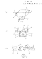
従来の電流検出装置としては図7〜図9に示すようなものが知られている(特許文献1参照)。図7(a)は従来の電流検出装置の外観斜視図を示したもので、この電流検出装置は樹脂製のケース1のトンネル部分2に導体3を通した後、ケース1ごとフランジ4で車両(図示せず)のボディ等に取り付け固定される。図7(b)は図7(a)におけるA−A線断面図を示したもので、補償電流線5と磁気抵抗素子部6および永久磁石7が所定の位置関係を保つように樹脂成形によって形成されたホルダー8で固定されている。9は前記導体3に流れる電流から発生した磁束を収束するための磁気ヨークで、磁性材などからなる。10は回路を構成する回路部品を搭載した回路基板である。   As conventional current detection devices, those shown in FIGS. 7 to 9 are known (see Patent Document 1). FIG. 7A shows an external perspective view of a conventional current detection device. The current detection device passes a conductor 3 through a tunnel portion 2 of a resin-made case 1, and then the vehicle is moved by the flange 4 together with the case 1. It is attached and fixed to a body or the like (not shown). FIG. 7B is a cross-sectional view taken along the line AA in FIG. 7A, and is formed by resin molding so that the compensation current line 5, the magnetoresistive element portion 6, and the permanent magnet 7 maintain a predetermined positional relationship. It is fixed by the formed holder 8. Reference numeral 9 denotes a magnetic yoke for converging the magnetic flux generated from the current flowing through the conductor 3, and is made of a magnetic material or the like. Reference numeral 10 denotes a circuit board on which circuit components constituting the circuit are mounted.

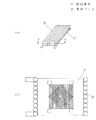
図8(a)は磁気抵抗素子部の構造と印加される磁界の方向を示すものである。図8(a)に示す磁気抵抗素子部6は絶縁基板11上に磁気抵抗薄膜をつづら折りに複数回折り返して磁気指向性を持たせた磁気抵抗素子6a,6b,6c,6dをそれぞれ図のように互いに電流の流れる方向を直交させて配置し、ブリッジ構成となるように接続して外部への引出し電極A、B、C、Dを設けて構成されている。ベクトルαは永久磁石7により発生されるバイアス磁界を示し、磁気抵抗素子6a,6b,6c,6dの磁気−抵抗特性における動作点を決定している。ベクトルβ、γは各々導体3、補償電流線5に流れる電流により磁気抵抗素子6a,6b,6c,6dに印加される磁界を示したものである。また、図8(b)は磁気抵抗素子部6の電気的等価回路図を示したものである。   FIG. 8A shows the structure of the magnetoresistive element portion and the direction of the applied magnetic field. In the magnetoresistive element section 6 shown in FIG. 8A, the magnetoresistive elements 6a, 6b, 6c, and 6d, each of which has a magnetic directivity by bending a plurality of magnetoresistive thin films back on the insulating substrate 11, are shown in the figure. Are arranged so that the directions of current flow are orthogonal to each other, connected to form a bridge configuration, and lead-out electrodes A, B, C, and D are provided to the outside. A vector α indicates a bias magnetic field generated by the permanent magnet 7 and determines an operating point in the magneto-resistance characteristics of the magnetoresistive elements 6a, 6b, 6c, and 6d. The vectors β and γ indicate the magnetic fields applied to the magnetoresistive elements 6a, 6b, 6c and 6d by the current flowing through the conductor 3 and the compensation current line 5, respectively. FIG. 8B shows an electrical equivalent circuit diagram of the magnetoresistive element section 6.

図9は上記従来の電流検出装置の動作を説明するための回路図である。前記磁気抵抗素子部6における磁気抵抗素子6a,6bの結合点Aと磁気抵抗素子6c,6dの結合点D間には定電圧を印加する電源12が接続されている。13は磁気抵抗素子6a,6dの結合点Cと、磁気抵抗素子6b,6cの結合点Bの電位差を検出する検出部で、この検出部13の出力信号によって電流制御部14が補償電流線5に流れる電流を制御している。15は出力変換部で、この出力変換部15は補償電流線5に流れる電流による負荷抵抗16での電圧降下を増幅して出力端子17に出力するものである。   FIG. 9 is a circuit diagram for explaining the operation of the conventional current detecting device. A power supply 12 for applying a constant voltage is connected between a coupling point A of the magnetoresistive elements 6a and 6b and a coupling point D of the magnetoresistive elements 6c and 6d in the magnetoresistive element section 6. Reference numeral 13 denotes a detection unit that detects a potential difference between the coupling point C of the magnetoresistive elements 6a and 6d and the coupling point B of the magnetoresistive elements 6b and 6c. The current control unit 14 uses the output signal of the detection unit 13 to make the compensation current line 5 The current that flows in the is controlled. Reference numeral 15 denotes an output converter, which amplifies a voltage drop at the load resistor 16 due to a current flowing through the compensation current line 5 and outputs the amplified voltage drop to the output terminal 17.

導体3に流れる電流が零の時、図8(a)に示したバイアス磁界αのみが磁気抵抗素子6a,6b,6c,6dに対して一定の角度(45度)をなすよう印加されるため、磁気抵抗素子6a,6b,6c,6dは実質的に同一の抵抗値となる。このため、磁気抵抗素子ブリッジは平衡し、磁気抵抗素子6a,6dの結合点Cと、磁気抵抗素子6b,6cの結合点Bは同電位となり、検出部13から信号は出力されない。これにより、補償電流線5と負荷抵抗16に電流が流れないため、出力端子17に出力電圧は現れないことになる。   When the current flowing through the conductor 3 is zero, only the bias magnetic field α shown in FIG. 8A is applied so as to form a certain angle (45 degrees) with respect to the magnetoresistive elements 6a, 6b, 6c and 6d. The magnetoresistive elements 6a, 6b, 6c and 6d have substantially the same resistance value. For this reason, the magnetoresistive element bridge is balanced, and the coupling point C of the magnetoresistive elements 6 a and 6 d and the coupling point B of the magnetoresistive elements 6 b and 6 c have the same potential, and no signal is output from the detection unit 13. As a result, no current flows through the compensation current line 5 and the load resistor 16, so that no output voltage appears at the output terminal 17.

一方、導体3に電流が流れると、図8(a)に示した磁界βが発生して磁気抵抗素子6a,6b,6c,6dに印加されるため、磁気抵抗素子6a,6cの抵抗は大きくなるとともに、磁気抵抗素子6b,6dの抵抗は小さくなる。このため、磁気抵抗素子ブリッジの平衡が破れ、磁気抵抗素子6a,6dの結合点Cと、磁気抵抗素子6b,6cの結合点Bとの間に電位差が発生する。この電位差は検出部13で検出されて電流制御部14に入力される。そして、この電流制御部14はこの電位差に基づいて補償電流線5に電流を流して、図8(a)に示した磁界γを発生させ、導体3から受ける磁界βを相殺し、磁気抵抗素子6a,6b,6c,6dに印加される正味の磁界を永久磁石7により発生される磁界αのみとすることにより、磁気抵抗素子ブリッジの電位差を零にするように動作する。このようにして再び磁気抵抗素子ブリッジが平衡した時、負荷抵抗16の両端に発生する電圧をモニターし適度に増幅すれば、導体3に流れる電流に対応した信号が出力端子17に出力されることになる。   On the other hand, when a current flows through the conductor 3, the magnetic field β shown in FIG. 8A is generated and applied to the magnetoresistive elements 6a, 6b, 6c, and 6d. Therefore, the resistance of the magnetoresistive elements 6a and 6c is large. At the same time, the resistances of the magnetoresistive elements 6b and 6d are reduced. For this reason, the balance of the magnetoresistive element bridge is broken, and a potential difference is generated between the coupling point C of the magnetoresistive elements 6a and 6d and the coupling point B of the magnetoresistive elements 6b and 6c. This potential difference is detected by the detection unit 13 and input to the current control unit 14. Then, the current control unit 14 causes a current to flow through the compensation current line 5 based on this potential difference, generates the magnetic field γ shown in FIG. 8A, cancels out the magnetic field β received from the conductor 3, and magnetoresistive element The net magnetic field applied to 6a, 6b, 6c, and 6d is only the magnetic field α generated by the permanent magnet 7, thereby operating the magnetoresistive element bridge to have a potential difference of zero. When the magnetoresistive element bridge is balanced again in this way, a signal corresponding to the current flowing through the conductor 3 is output to the output terminal 17 if the voltage generated at both ends of the load resistor 16 is monitored and amplified appropriately. become.

一般に磁気抵抗素子は磁気感度が高いという特徴を有する反面、磁気抵抗素子に印加される磁界の変化に対する磁気抵抗の変化が非直線的であるとともに、温度や経時等に伴い特性劣化が発生する場合があるという課題があった。これに対し、上記従来の電流検出装置においては、導体3に電流が流れている時であっても磁気抵抗素子6a,6b,6c,6dに印加される磁界は実質的に永久磁石7により発生される一定の磁界αのみとなるため、磁気抵抗素子の有する非直線的な磁気−抵抗特性および温度、経時等による特性劣化は電流検出装置としての特性にまったく関与せず、導体3に流れる電流と電流検出装置の出力信号との間の直線性が良好に保たれることになる。   In general, magnetoresistive elements are characterized by high magnetic sensitivity, but changes in magnetoresistance with respect to changes in the magnetic field applied to the magnetoresistive elements are non-linear, and characteristic deterioration occurs with temperature, time, etc. There was a problem that there was. On the other hand, in the conventional current detection device, the magnetic field applied to the magnetoresistive elements 6a, 6b, 6c and 6d is substantially generated by the permanent magnet 7 even when a current is flowing through the conductor 3. Therefore, the non-linear magneto-resistance characteristic of the magnetoresistive element and the characteristic deterioration due to temperature, time, etc. are not involved in the characteristic as the current detection device at all, and the current flowing through the conductor 3 And the linearity between the output signals of the current detectors are kept good.

なお、この出願の発明に関する先行技術文献情報としては、例えば、特許文献1が知られている。   As prior art document information relating to the invention of this application, for example, Patent Document 1 is known.

特開平7−92199号公報Japanese Unexamined Patent Publication No. 7-92199

しかしながら、上記図7〜図9に示した従来の電流検出装置においては、導体3に大電流が流れると、それに応じて補償電流線5に流すべき電流が大きくなるためセンサの消費電流が大きくなってしまうという問題点があった。図7(b)を用いてこの問題点を説明する。一般に電流線路の周りに発生する磁界の強さHは電流線路に流れる電流に比例し、電流線路からの距離に反比例する。よって、仮に図7(b)において、10Aの電流が流れている導体3と磁気抵抗素子部6との実効的な距離が20mmであり、補償電流線5と磁気抵抗素子部6との距離が1mmとすれば、補償電流線5には0.5Aという大きな電流を流さなければならないことになる。導体3と磁気抵抗素子部6との実効的な距離を大きくすれば、補償電流線5に流す電流を小さくすることができるが、この場合はセンサ自体の形状寸法が大きくなってしまうことになる。   However, in the conventional current detection apparatus shown in FIGS. 7 to 9, when a large current flows through the conductor 3, the current to be passed through the compensation current line 5 increases accordingly, so that the current consumption of the sensor increases. There was a problem that it was. This problem will be described with reference to FIG. In general, the strength H of the magnetic field generated around the current line is proportional to the current flowing through the current line and inversely proportional to the distance from the current line. Therefore, in FIG. 7B, the effective distance between the conductor 3 through which a current of 10 A flows and the magnetoresistive element unit 6 is 20 mm, and the distance between the compensation current line 5 and the magnetoresistive element unit 6 is If it is 1 mm, a large current of 0.5 A must flow through the compensation current line 5. If the effective distance between the conductor 3 and the magnetoresistive element portion 6 is increased, the current flowing through the compensation current line 5 can be reduced. In this case, however, the shape of the sensor itself is increased. .

本発明は上記従来の問題点を解決するもので、消費電流が小さく、かつ小形で、出力の直線性が良好な電流検出装置を提供することを目的とするものである。   SUMMARY OF THE INVENTION The present invention solves the above-described conventional problems, and an object of the present invention is to provide a current detection device that consumes less current, is small, and has excellent output linearity.

上記目的を達成するために、本発明は以下の構成を有するものである。   In order to achieve the above object, the present invention has the following configuration.

本発明の請求項1に記載の発明は、導体に流れる電流を検出する電流検出装置であって、絶縁基板と、前記絶縁基板上に配設され、かつ隣接する磁気抵抗素子の磁気検出方向が互いに直交する状態でブリッジ状に結合された4個の磁気抵抗素子と、前記磁気抵抗素子に近接して前記絶縁基板上に配設され、かつ前記磁気抵抗素子の磁気検出方向に対して略45度をなす方向にバイアス磁界を与える磁界発生手段と、前記磁気抵抗素子に近接して前記絶縁基板上に配設された補償電流線とからなる磁気抵抗素子センサと、前記磁気抵抗素子の相対向する2つの結合部間に定電圧を印加する電源と、前記電源により定電圧が印加されている結合部間以外の相対向する結合部間の電位差を検出する検出手段と、前記検出手段からの出力信号に基づいて前記電位差を零にするように前記補償電流線に流れる電流を制御する電流制御手段と、前記補償電流線に流れる電流を変換して出力する回路部とを備え、前記バイアス磁界方向と前記導体に流れる電流の方向とを平行とし、かつ前記導体に流れる電流によって生ずる磁界の方向に対して前記絶縁基板の法線方向を傾斜させたもので、この構成によれば、前記導体に流れる電流によって生ずる磁界が磁気抵抗素子に対して傾斜して印加されるため、前記導体に流れる電流によって生ずる磁界の磁気抵抗素子に作用する成分を等価的に減少させることができ、これにより、検出装置の形状を大きくすることなく、被測定電流を直線性よく低消費電流で測定することができるという作用効果を有するものである。   According to a first aspect of the present invention, there is provided a current detecting device for detecting a current flowing through a conductor, wherein an insulating substrate and a magnetic detection direction of an adjacent magnetoresistive element disposed on the insulating substrate are set. Four magnetoresistive elements coupled in a bridge shape orthogonal to each other, and disposed on the insulating substrate in the vicinity of the magnetoresistive element, and approximately 45 with respect to the magnetic detection direction of the magnetoresistive element. A magnetoresistive element sensor comprising a magnetic field generating means for applying a bias magnetic field in a direction in which the magnetoresistive element is disposed; a compensation current line disposed on the insulating substrate in the vicinity of the magnetoresistive element; A power source that applies a constant voltage between the two coupling portions, a detection means that detects a potential difference between opposing coupling portions other than between the coupling portions to which a constant voltage is applied by the power source, and Based on output signal Current control means for controlling the current flowing through the compensation current line so as to make the potential difference zero, and a circuit unit for converting and outputting the current flowing through the compensation current line, and the bias magnetic field direction and the conductor The direction of the flowing current is parallel, and the normal direction of the insulating substrate is inclined with respect to the direction of the magnetic field generated by the current flowing through the conductor. According to this configuration, the direction of current flowing through the conductor is generated. Since the magnetic field is applied with an inclination to the magnetoresistive element, the component acting on the magnetoresistive element of the magnetic field generated by the current flowing through the conductor can be reduced equivalently, thereby reducing the shape of the detection device. The effect is that the current to be measured can be measured with good linearity and low current consumption without increasing it.

本発明の請求項2に記載の発明は、導体に流れる電流を検出する電流検出装置であって、絶縁基板と、前記絶縁基板上に配設され、かつ隣接する磁気抵抗素子の磁気検出方向が互いに直交する状態でブリッジ状に結合された4個の磁気抵抗素子と、前記磁気抵抗素子に近接して前記絶縁基板上に配設され、かつ前記磁気抵抗素子の磁気検出方向に対して略45度をなす方向にバイアス磁界を与える磁界発生手段と、前記磁気抵抗素子に近接して前記絶縁基板上に配設された補償電流線とからなる2個以上の磁気抵抗素子センサと、前記2個以上の磁気抵抗素子センサのうちから選択されたいずれかの磁気抵抗素子センサにおける磁気抵抗素子の相対向する2つの結合部間だけに定電圧を印加する電源と、前記選択された磁気抵抗素子センサにおける前記電源により定電圧が印加されている結合部間以外の相対向する結合部間の電位差を検出する検出手段と、前記選択された磁気抵抗素子センサにおける前記検出手段からの出力信号に基づいて前記電位差を零にするように前記補償電流線に流れる電流を制御する電流制御手段とを備え、前記磁気抵抗素子センサの1つは、前記バイアス磁界方向と前記導体に流れる電流の方向とを平行とし、かつ前記導体に流れる電流によって生ずる磁界の方向に対して前記磁気抵抗素子センサにおける絶縁基板の法線方向を直交させるとともに、他の磁気抵抗素子センサは、前記導体に流れる電流によって生ずる磁界の方向に対して前記磁気抵抗素子センサにおける絶縁基板の法線方向を傾斜させたもので、この構成によれば、前記導体に流れる電流が小さい時には、磁気抵抗素子の絶縁基板の法線方向と、導体に流れる電流によって生ずる磁界とが直交するように配置された磁気抵抗素子センサを選択し、一方、前記導体に流れる電流が大きい時には、磁気抵抗素子の絶縁基板の法線方向と、導体に流れる電流によって生ずる磁界が傾斜するように配置された磁気抵抗素子センサを選択することにより、検出装置の形状を大きくすることなく、広い範囲の被測定電流を直線性よく低消費電流で測定することができるという作用効果を有するものである。   According to a second aspect of the present invention, there is provided a current detecting device for detecting a current flowing through a conductor, wherein an insulating substrate and a magnetic detection direction of an adjacent magnetoresistive element disposed on the insulating substrate are set. Four magnetoresistive elements coupled in a bridge shape orthogonal to each other, and disposed on the insulating substrate in the vicinity of the magnetoresistive element, and approximately 45 with respect to the magnetic detection direction of the magnetoresistive element. Two or more magnetoresistive element sensors comprising magnetic field generating means for applying a bias magnetic field in a direction in which the magnetic field is generated; and a compensation current line disposed on the insulating substrate in the vicinity of the magnetoresistive element; A power supply that applies a constant voltage only between two opposing coupling portions of the magnetoresistive element in any one of the magnetoresistive element sensors selected from the above magnetoresistive element sensors, and the selected magnetoresistive element sensor In Detecting means for detecting a potential difference between opposite coupling portions other than between the coupling portions to which a constant voltage is applied by the power source, and based on an output signal from the detection means in the selected magnetoresistive element sensor Current control means for controlling the current flowing through the compensation current line so that the potential difference becomes zero, and one of the magnetoresistive element sensors has the bias magnetic field direction parallel to the direction of the current flowing through the conductor. And the normal direction of the insulating substrate in the magnetoresistive element sensor is orthogonal to the direction of the magnetic field generated by the current flowing in the conductor, and the other magnetoresistive element sensors have a magnetic field generated by the current flowing in the conductor. The normal direction of the insulating substrate in the magnetoresistive element sensor is inclined with respect to the direction. According to this configuration, the current flowing in the conductor is Is selected, the magnetoresistive element sensor arranged so that the normal direction of the insulating substrate of the magnetoresistive element and the magnetic field generated by the current flowing through the conductor are orthogonal to each other, while the current flowing through the conductor is large By selecting a magnetoresistive element sensor arranged so that the normal direction of the insulating substrate of the magnetoresistive element and the magnetic field generated by the current flowing through the conductor are inclined, a wide range without increasing the shape of the detection device The current to be measured can be measured with good linearity and low current consumption.

本発明の請求項3に記載の発明は、特に、磁界発生手段として薄膜磁石を用いたもので、この構成によれば、薄膜磁石を磁気抵抗素子上にスパッタ等の手段で形成し、そして、フォトリソグラフィ技術を用いてパターニングして形成することにより、磁界発生手段と磁気抵抗素子とを一体的に互いにきわめて近接させて、かつ精度よく配置することができるため、被測定電流をさらに高精度で測定することができるという作用効果を有するものである。   The invention described in claim 3 of the present invention particularly uses a thin film magnet as the magnetic field generating means. According to this configuration, the thin film magnet is formed on the magnetoresistive element by means such as sputtering, and By patterning using photolithography technology, the magnetic field generating means and the magnetoresistive element can be integrally and extremely close to each other, and can be arranged with high precision, so that the current to be measured can be further accurately It has the effect that it can be measured.

本発明の請求項4に記載の発明は、特に、補償電流線として巻線コイルを用いたもので、この構成によれば、補償電流線に流れる電流により発生させる磁界を巻線のターン数倍だけ増大させることができるため、補償電流線に流す電流をさらに小さくでき、これにより、被測定電流を直線性よくさらに低消費電流で測定することができるという作用効果を有するものである。   The invention described in claim 4 of the present invention uses a winding coil as the compensation current line. According to this configuration, the magnetic field generated by the current flowing through the compensation current line is multiplied by the number of turns of the winding. Since the current flowing through the compensation current line can be further reduced, the current to be measured can be measured with good linearity and low current consumption.

以上のように本発明の物理量センサは、導体に流れる電流を検出する電流検出装置であって、絶縁基板と、前記絶縁基板上に配設され、かつ隣接する磁気抵抗素子の磁気検出方向が互いに直交する状態でブリッジ状に結合された4個の磁気抵抗素子と、前記磁気抵抗素子に近接して前記絶縁基板上に配設され、かつ前記磁気抵抗素子の磁気検出方向に対して略45度をなす方向にバイアス磁界を与える磁界発生手段と、前記磁気抵抗素子に近接して前記絶縁基板上に配設された補償電流線とからなる磁気抵抗素子センサと、前記磁気抵抗素子の相対向する2つの結合部間に定電圧を印加する電源と、前記電源により定電圧が印加されている結合部間以外の相対向する結合部間の電位差を検出する検出手段と、前記検出手段からの出力信号に基づいて前記電位差を零にするように前記補償電流線に流れる電流を制御する電流制御手段と、前記補償電流線に流れる電流を変換して出力する回路部とを備え、前記バイアス磁界方向と前記導体に流れる電流の方向とを平行とし、かつ前記導体に流れる電流によって生ずる磁界の方向に対して前記絶縁基板の法線方向を傾斜させたもので、前記導体に流れる電流によって生ずる磁界が磁気抵抗素子に対して傾斜して印加されるため、前記導体に流れる電流によって生ずる磁界の磁気抵抗素子に作用する成分を等価的に減少させることができ、これにより、検出装置の形状を大きくすることなく、被測定電流を直線性よく低消費電流で測定することができるという優れた効果を奏するものである。   As described above, the physical quantity sensor of the present invention is a current detection device that detects a current flowing through a conductor, and the magnetic detection directions of the insulating substrate and the adjacent magnetoresistive elements disposed on the insulating substrate are mutually Four magnetoresistive elements coupled in a bridge shape in an orthogonal state, and disposed on the insulating substrate in the vicinity of the magnetoresistive element, and approximately 45 degrees with respect to the magnetic detection direction of the magnetoresistive element. A magnetoresistive element sensor comprising a magnetic field generating means for applying a bias magnetic field in the direction of forming a magnetic field, a compensation current line disposed on the insulating substrate in the vicinity of the magnetoresistive element, and the magnetoresistive element facing each other. A power source for applying a constant voltage between two coupling portions; a detecting means for detecting a potential difference between opposing coupling portions other than between the coupling portions to which a constant voltage is applied by the power source; and an output from the detecting means Based on signal Current control means for controlling the current flowing through the compensation current line so as to make the potential difference zero, and a circuit unit for converting and outputting the current flowing through the compensation current line, the bias magnetic field direction and the conductor The direction of the current flowing through the conductor is parallel, and the normal direction of the insulating substrate is inclined with respect to the direction of the magnetic field generated by the current flowing through the conductor. Applied to the magnetic field, the component acting on the magnetoresistive element of the magnetic field generated by the current flowing in the conductor can be equivalently reduced, and without increasing the shape of the detection device, This provides an excellent effect that the current to be measured can be measured with good linearity and low current consumption.

(a)本発明の実施の形態1における電流検出装置の斜視図、(b)(a)におけるB−B線断面図(A) Perspective view of current detection device according to embodiment 1 of the present invention, (b) Cross-sectional view along line BB in (a) (a)同電流検出装置における磁気抵抗素子センサの上面図、(b)(a)におけるC−C線断面図(A) Top view of magnetoresistive element sensor in the same current detection device, (b) CC sectional view in (a) 同電流検出装置における磁気抵抗素子センサ近傍の拡大断面図Enlarged sectional view of the vicinity of the magnetoresistive element sensor in the same current detection device 同電流検出装置の動作を説明するための回路図Circuit diagram for explaining the operation of the current detection device (a)本発明の実施の形態2における電流検出装置の斜視図、(b)(a)におけるD−D線断面図、(c)(b)におけるA部拡大図(A) Perspective view of current detection device according to embodiment 2 of the present invention, (b) A sectional view taken along the line DD in (a), and an enlarged view of portion A in (c) and (b) (a)本発明の実施の形態3における電流検出装置の磁気抵抗素子センサを示す斜視図、(b)(a)におけるE−E線断面図(A) The perspective view which shows the magnetoresistive element sensor of the electric current detection apparatus in Embodiment 3 of this invention, (b) The EE sectional view taken on the line in (a) (a)従来の電流検出装置の斜視図、(b)(a)におけるA−A線断面図(A) Perspective view of conventional current detection device, (b) AA line sectional view in (a) (a)同電流検出装置における磁気抵抗素子部の構造と印加される磁界の方向を示す図、(b)同磁気抵抗素子部の電気的等価回路図(A) The figure which shows the structure of the magnetoresistive element part in the same electric current detection apparatus, and the direction of the applied magnetic field, (b) The electrical equivalent circuit schematic of the magnetoresistive element part 同電流検出装置の動作を説明するための回路図Circuit diagram for explaining the operation of the current detection device

(実施の形態1)
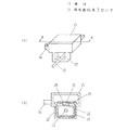
以下、実施の形態1を用いて、本発明の特に請求項1,3に記載の発明について説明する。図1(a)は本発明の実施の形態1における電流検出装置の斜視図を示したもので、この電流検出装置は樹脂製のケース21のトンネル部分22に導体23を通した後、ケース21ごとフランジ24で車両(図示せず)のボディ等に取り付け固定される。図1(b)は図1(a)におけるB−B線断面図を示したもので、磁気抵抗素子センサ25が樹脂成形によって形成された台座26の上に固定されている。27は被測定電流から発生した磁束を収束するための磁気ヨークで、この磁気ヨーク27は磁性薄膜などからなり、そして、前記磁気抵抗素子センサ25はこの磁気ヨーク27内に形成されたギャップ28内に配置されている。また、29は回路部品(図示せず)が搭載された回路基板である。そして、前記導体23に被測定電流が流れると、導体23の周囲に磁界が発生する。この磁界は磁気ヨーク27内に閉じ込められ、ギャップ28内に均一に放射される。また、前記磁気抵抗素子センサ25はこうしてギャップ28内に形成された磁界に対してその絶縁基板の法線方向を傾斜して配置されているものである。
(Embodiment 1)
Hereinafter, the first and third aspects of the present invention will be described with reference to the first embodiment. FIG. 1A shows a perspective view of a current detection device according to Embodiment 1 of the present invention. This current detection device passes a conductor 23 through a tunnel portion 22 of a resin case 21, and then the case 21 Each flange 24 is attached and fixed to the body of a vehicle (not shown). FIG. 1B is a sectional view taken along line BB in FIG. 1A, and a magnetoresistive element sensor 25 is fixed on a pedestal 26 formed by resin molding. Reference numeral 27 denotes a magnetic yoke for converging the magnetic flux generated from the current to be measured. The magnetic yoke 27 is made of a magnetic thin film and the like, and the magnetoresistive element sensor 25 is placed in a gap 28 formed in the magnetic yoke 27. Is arranged. Reference numeral 29 denotes a circuit board on which circuit components (not shown) are mounted. When a current to be measured flows through the conductor 23, a magnetic field is generated around the conductor 23. This magnetic field is confined in the magnetic yoke 27 and radiated uniformly in the gap 28. The magnetoresistive element sensor 25 is arranged so that the normal direction of the insulating substrate is inclined with respect to the magnetic field formed in the gap 28 in this way.

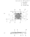
図2(a)は前記磁気抵抗素子センサ25の上面図、図2(b)は図2(a)におけるC−C線断面図である。図2(a)(b)において、30a,30b,30c,30dはセラミック等の絶縁基板31上に形成された磁気抵抗素子であり、これらはNi−Co等の強磁性体からなる厚み約0.1μmの磁気抵抗薄膜である。そして、前記磁気抵抗素子30a,30bおよび磁気抵抗素子30c,30dは各々直列に接続され、磁気検出方向であるパターンの長手方向が互いに直交している。入力電極32aは絶縁基板31上に形成されているもので、前記磁気抵抗素子30aおよび磁気抵抗素子30dと電気的に接続されている。第1の出力電極32bも絶縁基板31上に形成されており、前記磁気抵抗素子30aおよび磁気抵抗素子30bと電気的に接続されている。同様にしてグランド電極32c、第2の出力電極32dも絶縁基板31上に形成されており、各々前記磁気抵抗素子30bおよび磁気抵抗素子30c、前記磁気抵抗素子30cおよび磁気抵抗素子30dと電気的に接続されている。   2A is a top view of the magnetoresistive element sensor 25, and FIG. 2B is a cross-sectional view taken along line CC in FIG. 2A. 2A and 2B, 30a, 30b, 30c, and 30d are magnetoresistive elements formed on an insulating substrate 31 such as ceramic, and these have a thickness of about 0 made of a ferromagnetic material such as Ni-Co. .1 μm magnetoresistive thin film. The magnetoresistive elements 30a and 30b and the magnetoresistive elements 30c and 30d are connected in series, and the longitudinal directions of the patterns, which are the magnetic detection directions, are orthogonal to each other. The input electrode 32a is formed on the insulating substrate 31, and is electrically connected to the magnetoresistive element 30a and the magnetoresistive element 30d. The first output electrode 32b is also formed on the insulating substrate 31, and is electrically connected to the magnetoresistive element 30a and the magnetoresistive element 30b. Similarly, the ground electrode 32c and the second output electrode 32d are also formed on the insulating substrate 31, and are electrically connected to the magnetoresistive element 30b and the magnetoresistive element 30c, and the magnetoresistive element 30c and the magnetoresistive element 30d, respectively. It is connected.

33aは第1の絶縁層で、この第1の絶縁層33aは厚みが約1μmのSiO2薄膜からなり、前記磁気抵抗素子30a,30b,30c,30dを覆うことにより後述する薄膜磁石34からなるバイアス磁界発生手段との電気的絶縁を行うものである。 Reference numeral 33a denotes a first insulating layer, and the first insulating layer 33a is made of a SiO 2 thin film having a thickness of about 1 μm, and is made of a thin film magnet 34 described later by covering the magnetoresistive elements 30a, 30b, 30c, 30d. It electrically insulates from the bias magnetic field generating means.

34は薄膜磁石で、この薄膜磁石34は厚みが約0.6μmのCoPt等からなり、前記第1の絶縁層33aの上に蒸着、スパッタ法等により形成した後、露光、エッチングによりパターニングすることにより、前記磁気抵抗素子30a,30b,30c,30dの磁気検出方向と45度をなす方向に長手方向を有する複数の略長方体に分割されているものである。そして、この複数の略長方体形状の薄膜の幅方向にきわめて大きな磁界を印加することにより、略長方体形状の薄膜が幅方向に磁化されて、薄膜磁石34を得ることができる。XYZ軸を図2(a)に示すように規定した時、薄膜磁石34からはY軸方向の磁界が発生し、磁気抵抗素子30a,30b,30c,30dの磁気検出方向に対して45度をなす方向にバイアス磁界が印加されることになる。   Reference numeral 34 denotes a thin film magnet. The thin film magnet 34 is made of CoPt or the like having a thickness of about 0.6 μm. The thin film magnet 34 is formed on the first insulating layer 33a by vapor deposition or sputtering, and then patterned by exposure and etching. Thus, the magnetic resistance elements 30a, 30b, 30c, and 30d are divided into a plurality of substantially rectangular parallelepipeds having a longitudinal direction in a direction that forms 45 degrees with the magnetic detection direction. Then, by applying an extremely large magnetic field in the width direction of the plurality of substantially rectangular thin films, the thin film having a substantially rectangular shape is magnetized in the width direction, and the thin film magnet 34 can be obtained. When the XYZ axes are defined as shown in FIG. 2A, a magnetic field in the Y-axis direction is generated from the thin film magnet 34, and 45 degrees with respect to the magnetic detection direction of the magnetoresistive elements 30a, 30b, 30c, 30d. A bias magnetic field is applied in the direction formed.

33bは第2の絶縁層で、この第2の絶縁層33bは厚みが約1μmのSiO2薄膜からなり、前記薄膜磁石34を覆うことにより後述する補償電流線35との電気的絶縁を行うものである。 Reference numeral 33b denotes a second insulating layer, and the second insulating layer 33b is made of a SiO 2 thin film having a thickness of about 1 μm, and electrically insulates from a compensation current line 35 described later by covering the thin film magnet 34. It is.

35は補償電流線で、この補償電流線35は厚みが約0.6μmの銅薄膜からなり、前記第2の絶縁層33bの上に蒸着法等により形成した後、露光、エッチングによりパターニングすることにより形成している。   Reference numeral 35 denotes a compensation current line. This compensation current line 35 is made of a copper thin film having a thickness of about 0.6 μm, and is formed on the second insulating layer 33b by vapor deposition or the like, and then patterned by exposure and etching. It is formed by.

上記したような構成とすることにより、絶縁基板31の上に磁気抵抗素子30a,30b,30c,30d、薄膜磁石34、補償電流線35を一体的に互いにきわめて近接させて、かつ精度よく配置することができるものである。   With the above-described configuration, the magnetoresistive elements 30a, 30b, 30c, and 30d, the thin film magnet 34, and the compensation current line 35 are integrally and extremely close to each other on the insulating substrate 31 with high accuracy. It is something that can be done.

図3は図1(b)の磁気抵抗素子センサ25の近傍を拡大して示したもので、この図3において、HIは導体23に流れる電流により磁気ヨーク27のギャップ28内に発生した磁界を示し、前記磁気抵抗素子センサ25はこの磁界HIに対して前記磁気抵抗素子センサにおける絶縁基板の法線方向を角度θだけ傾斜させている。磁気抵抗素子センサ25に対してXYZ軸を図2(a)と同様に規定すると、薄膜磁石34から発生するバイアス磁界HBはY軸方向に印加される。また、Hcは補償電流線35に流れる電流により発生する磁界であり、X軸方向内にある。 Figure 3 is an illustration on an enlarged scale the vicinity of the magnetoresistive element sensor 25 of FIG. 1 (b), the magnetic field in FIG. 3, H I is generated in the gap 28 of the magnetic yoke 27 by the current flowing in the conductor 23 are shown, the magnetoresistive element sensor 25 is a normal direction of the insulating substrate is inclined by an angle θ in the magnetoresistive element sensor relative to the magnetic field H I. When the XYZ axes are defined for the magnetoresistive element sensor 25 in the same manner as in FIG. 2A, the bias magnetic field H B generated from the thin film magnet 34 is applied in the Y axis direction. H c is a magnetic field generated by the current flowing through the compensation current line 35 and is in the X-axis direction.

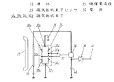
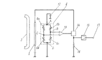
図4は本発明の実施の形態1における電流検出装置の動作を説明するための回路図を示したもので、この図4に示すように、前記磁気抵抗素子センサ25の入力電極32aとグランド電極32cとの間には定電圧を印加する電源36が接続されている。また、この図4において、37は第1の出力電極32bと第2の出力電極32dの電位差を検出する検出部で、この検出部37の出力信号によって電流制御部38が補償電流線35に流れる電流を制御している。39は出力変換部で、この出力変換部39は前記補償電流線35に流れる電流による負荷抵抗40での電圧降下を増幅して出力端子41に出力するものである。   FIG. 4 is a circuit diagram for explaining the operation of the current detecting device according to the first embodiment of the present invention. As shown in FIG. 4, the input electrode 32a and the ground electrode of the magnetoresistive element sensor 25 are shown. A power source 36 for applying a constant voltage is connected between the power source 32c and the terminal 32c. In FIG. 4, reference numeral 37 denotes a detection unit that detects a potential difference between the first output electrode 32 b and the second output electrode 32 d, and the current control unit 38 flows to the compensation current line 35 by the output signal of the detection unit 37. The current is controlled. Reference numeral 39 denotes an output conversion unit, which amplifies a voltage drop at the load resistor 40 due to a current flowing through the compensation current line 35 and outputs the amplified voltage drop to the output terminal 41.

導体23に流れる電流が零の時、図3に示したバイアス磁界HBのみが磁気抵抗素子30a,30b,30c,30dに対して一定の角度(45度)をなすように印加されるため、磁気抵抗素子30a,30b,30c,30dは実質的に同一の抵抗値となる。このため、磁気抵抗素子ブリッジは平衡し、第1の出力電極32bと第2の出力電極32dは同電位となり、検出部37から信号は出力されない。これにより、補償電流線35と負荷抵抗40に電流が流れないため、出力端子41には出力電圧は現れないことになる。 When the current flowing through the conductor 23 is zero, only the bias magnetic field H B shown in FIG. 3 is applied at a certain angle (45 degrees) with respect to the magnetoresistive elements 30a, 30b, 30c, and 30d. The magnetoresistive elements 30a, 30b, 30c, and 30d have substantially the same resistance value. For this reason, the magnetoresistive element bridge is balanced, the first output electrode 32 b and the second output electrode 32 d have the same potential, and no signal is output from the detection unit 37. As a result, no current flows through the compensation current line 35 and the load resistor 40, so that no output voltage appears at the output terminal 41.

導体23に電流が流れると、図3に示した磁界HIが発生して磁気抵抗素子センサ25に印加され、磁気抵抗素子30a,30cの抵抗が小さくなるとともに、磁気抵抗素子30b,30dの抵抗が大きくなる。このため、磁気抵抗素子ブリッジの平衡が破れ、第1の出力電極32bと第2の出力電極32dとの間に電位差が発生する。この電位差は検出部37で検出されて電流制御部38に入力される。電流制御部38はこの電位差に基づいて補償電流線35に電流を流して、図3に示した磁界Hcを発生させ、磁気抵抗素子30a,30b,30c,30dに印加される正味の磁界を薄膜磁石34から発生するバイアス磁界HBのみとすることにより、磁気抵抗素子ブリッジの電位差を零にするように動作する。こうして再び磁気抵抗素子ブリッジが平衡した時、負荷抵抗40の両端に発生する電圧をモニターして適度に増幅すれば、導体23に流れる電流に対応した信号が出力端子41に出力されることになる。 When a current flows through the conductor 23, is applied to the magnetoresistive element sensor 25 a magnetic field H I shown is generated in FIG. 3, the magneto-resistive element 30a, with 30c of resistance decreases, the magnetoresistive element 30b, 30d of the resistor Becomes larger. For this reason, the balance of the magnetoresistive element bridge is broken, and a potential difference is generated between the first output electrode 32b and the second output electrode 32d. This potential difference is detected by the detection unit 37 and input to the current control unit 38. Based on this potential difference, the current control unit 38 causes a current to flow through the compensation current line 35 to generate the magnetic field H c shown in FIG. 3, and the net magnetic field applied to the magnetoresistive elements 30a, 30b, 30c, and 30d. By using only the bias magnetic field H B generated from the thin film magnet 34, the magnetoresistive element bridge operates to make the potential difference zero. Thus, when the magnetoresistive element bridge is balanced again, if the voltage generated at both ends of the load resistor 40 is monitored and amplified appropriately, a signal corresponding to the current flowing through the conductor 23 is output to the output terminal 41. .

このように、本発明の実施の形態1における電流検出装置においては、導体23に電流が流れている時であっても磁気抵抗素子30a,30b,30c,30dに印加される磁界は実質的に薄膜磁石34から発生する一定の磁界HBのみとなるため、磁気抵抗素子の有する非直線的な磁気−抵抗特性および温度、経時等による特性劣化が電流検出装置としての特性にまったく関与せず、導体23に流れる電流と電流検出装置の出力信号との間の直線性が良好に保たれることになる。 Thus, in the current detection device according to the first embodiment of the present invention, the magnetic field applied to the magnetoresistive elements 30a, 30b, 30c, and 30d is substantially equal even when a current is flowing through the conductor 23. Since only the constant magnetic field H B generated from the thin-film magnet 34 is present, the nonlinear magneto-resistance characteristics of the magnetoresistive element and the characteristics degradation due to temperature, time, etc. are not involved in the characteristics of the current detection device at all. The linearity between the current flowing through the conductor 23 and the output signal of the current detection device is kept good.

この場合、上記したように前記磁気抵抗素子センサ25は磁界HIに対して前記磁気抵抗素子センサにおける絶縁基板の法線方向を角度θだけ傾斜させているため、磁気抵抗素子30a,30b,30c,30dの磁気検出方向に印加される磁界の強さはHIcosθとなりHIよりも小さくなる。そのため、この磁界の強さHIcosθを相殺するために補償電流線35に流すべき電流は小さくてすむことになる。これにより、検出装置の形状を大きくすることなく、被測定電流を直線性よく低消費電流で測定することができるものである。 In this case, since the above as described above magnetoresistive element sensor 25 is inclined in the normal direction of the insulating substrate in the magnetoresistive element sensor relative to the magnetic field H I by an angle theta, magnetoresistive elements 30a, 30b, 30c , 30d, the strength of the magnetic field applied in the magnetic detection direction is H I cos θ, which is smaller than H I. For this reason, the current to be passed through the compensation current line 35 in order to cancel out this magnetic field strength H I cos θ is small. Thus, the current to be measured can be measured with good linearity and low current consumption without increasing the shape of the detection device.

(実施の形態2)
以下、実施の形態2を用いて、本発明の特に請求項2に記載の発明について説明する。図5(a)は本発明の実施の形態2における電流検出装置の斜視図、図5(b)は図5(a)におけるD−D線断面図、図5(c)は図5(b)のA部拡大図である。なお、この本発明の実施の形態2においては、上記した本発明の実施の形態1の構成と同様の構成を有するものについては、同一符号を付しており、その説明は省略する。
(Embodiment 2)
The second aspect of the present invention will be described below with reference to the second embodiment. 5A is a perspective view of the current detection device according to Embodiment 2 of the present invention, FIG. 5B is a cross-sectional view taken along the line DD in FIG. 5A, and FIG. 5C is FIG. FIG. In the second embodiment of the present invention, components having the same configuration as the configuration of the first embodiment of the present invention described above are denoted by the same reference numerals, and the description thereof is omitted.

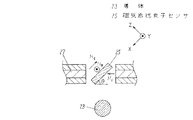
図5(a)(b)(c)において、本発明の実施の形態2が上記した本発明の実施の形態1と相違する点は、磁気ヨーク27内に形成されたギャップ28内において、図2で示した構成を有する複数の磁気抵抗素子センサ45,46が樹脂成形によって形成された台座47の上に配置され、そして前記磁気抵抗素子センサ45は導体23に流れる電流によって前記ギャップ28内に発生する磁界HIに対して前記磁気抵抗素子センサ45における絶縁基板の法線方向を角度θだけ傾斜させているとともに、前記磁気抵抗素子センサ46は磁界HIに対して前記磁気抵抗素子センサ46における絶縁基板の法線方向を直交させた点である。前記磁気抵抗素子センサ45,46における絶縁基板上に形成した薄膜磁石から発生するバイアス磁界HB1,HB2はともに紙面の垂直方向に印加されている。また、HC1,HC2は各々の磁気抵抗素子センサ45,46における絶縁基板上に形成した補償電流線に流れる電流により発生する磁界であり、各々の絶縁基板の表面に沿う方向に印加される。 5A, 5B, and 5C, the second embodiment of the present invention is different from the first embodiment of the present invention described above in the gap 28 formed in the magnetic yoke 27. FIG. 2 are arranged on a base 47 formed by resin molding, and the magnetoresistive element sensor 45 is placed in the gap 28 by a current flowing through the conductor 23. The normal direction of the insulating substrate in the magnetoresistive element sensor 45 is inclined by an angle θ with respect to the generated magnetic field H I , and the magnetoresistive element sensor 46 is in contact with the magnetic field H I. The normal line direction of the insulating substrate in FIG. Bias magnetic fields H B1 and H B2 generated from a thin film magnet formed on an insulating substrate in the magnetoresistive element sensors 45 and 46 are applied in a direction perpendicular to the paper surface. H C1 and H C2 are magnetic fields generated by a current flowing through a compensation current line formed on the insulating substrate in each of the magnetoresistive element sensors 45 and 46, and are applied in a direction along the surface of each insulating substrate. .

導体23に流れる電流が小さい時には、磁気抵抗素子センサ46の入力電極とグランド電極との間のみに定電圧が印加されるとともに、検出部37bの出力が電流制御部38に接続される。電流制御部38は磁気抵抗素子センサ46に印加される正味の磁界がバイアス磁界HB2のみとなるように補償電流線35に流れる電流を制御する。この電流によって負荷抵抗40の両端に発生する電圧をモニターして適度に増幅すれば、導体23に流れる電流に対応した信号が出力端子41に出力されることになる。被測定電流に流れる電流が大きくなると、磁気抵抗素子センサ45の入力電極とグランド電極との間のみに定電圧が印加されるとともに、検出部37aの出力が電流制御部38に接続される。電流制御部38は磁気抵抗素子センサ45に印加される正味の磁界がバイアス磁界HB1のみとなるように補償電流線35に流れる電流を制御する。この電流によって負荷抵抗40の両端に発生する電圧をモニターして適度に増幅すれば、導体23に流れる電流に対応した信号が出力端子41に出力されることになる。このような構成とすることにより、検出装置の形状を大きくすることなく、広い範囲の被測定電流を直線性よく低消費電流で測定することができるという効果が得られるものである。 When the current flowing through the conductor 23 is small, a constant voltage is applied only between the input electrode of the magnetoresistive element sensor 46 and the ground electrode, and the output of the detection unit 37b is connected to the current control unit 38. The current control unit 38 controls the current flowing through the compensation current line 35 so that the net magnetic field applied to the magnetoresistive element sensor 46 is only the bias magnetic field H B2 . If the voltage generated at both ends of the load resistor 40 is monitored and amplified appropriately by this current, a signal corresponding to the current flowing through the conductor 23 is output to the output terminal 41. When the current flowing through the current to be measured increases, a constant voltage is applied only between the input electrode of the magnetoresistive element sensor 45 and the ground electrode, and the output of the detection unit 37a is connected to the current control unit 38. The current control unit 38 controls the current flowing through the compensation current line 35 so that the net magnetic field applied to the magnetoresistive element sensor 45 is only the bias magnetic field H B1 . If the voltage generated at both ends of the load resistor 40 is monitored and amplified appropriately by this current, a signal corresponding to the current flowing through the conductor 23 is output to the output terminal 41. With such a configuration, it is possible to obtain an effect that a wide range of currents to be measured can be measured with high linearity and low current consumption without increasing the shape of the detection device.

なお、本発明の実施の形態1,2において使用した磁気ヨーク27を削除しても本発明の目的を達成することは可能であるが、磁気ヨーク27を使用しない場合には導体23から発生した磁界が外部に漏れないようにケース21を覆う磁気シールドを設けることが望ましい。   Although the object of the present invention can be achieved even if the magnetic yoke 27 used in the first and second embodiments of the present invention is deleted, it is generated from the conductor 23 when the magnetic yoke 27 is not used. It is desirable to provide a magnetic shield that covers the case 21 so that the magnetic field does not leak outside.

(実施の形態3)
以下、実施の形態3を用いて、本発明の特に請求項4に記載の発明について説明する。図6(a)は本発明の実施の形態3における電流検出装置の磁気抵抗素子センサを示す斜視図、図6(b)は図6(a)におけるE−E線断面図である。
(Embodiment 3)
The third embodiment of the present invention will be described below in particular. FIG. 6A is a perspective view showing a magnetoresistive element sensor of the current detection device according to Embodiment 3 of the present invention, and FIG. 6B is a cross-sectional view taken along line EE in FIG.

図6(a)(b)において、本発明の実施の形態3における電流検出装置の磁気抵抗素子センサが図2に示した本発明の実施の形態1,2における電流検出装置の磁気抵抗素子センサと相違する点は、巻線コイル50を絶縁基板31の周囲に巻回して補償電流線とした点である。このような構成とすることにより、補償電流線に流れる電流により発生する磁界を巻線のターン数倍だけ増大させることができるため、補償電流線に流す電流をさらに小さくでき、これにより、被測定電流を直線性よくさらに低消費電流で測定することができるという効果が得られるものである。   6A and 6B, the magnetoresistive element sensor of the current detecting device according to the third embodiment of the present invention is the magnetoresistive element sensor of the current detecting device according to the first and second embodiments of the present invention shown in FIG. The difference is that the winding coil 50 is wound around the insulating substrate 31 to form a compensation current line. By adopting such a configuration, the magnetic field generated by the current flowing through the compensation current line can be increased by the number of turns of the winding, so that the current flowing through the compensation current line can be further reduced. The effect is obtained that the current can be measured with good linearity and with low current consumption.

本発明の電流検出装置は、導体に流れる電流によって生ずる磁界の磁気抵抗素子に作用する成分を等価的に減少させることができ、これにより、検出装置の形状を大きくすることなく、被測定電流を直線性よく低消費電流で測定することができるという効果を有するものであり、特に、車両、産業機器等内における電流を検出する電流検出装置として有用なものである。   The current detection device of the present invention can equivalently reduce the component acting on the magnetoresistive element of the magnetic field generated by the current flowing through the conductor, thereby reducing the current to be measured without increasing the shape of the detection device. It has the effect of being able to measure with low current consumption with good linearity, and is particularly useful as a current detection device for detecting current in vehicles, industrial equipment and the like.

23 導体
25 磁気抵抗素子センサ
30a,30b,30c,30d 磁気抵抗素子
31 絶縁基板
34 薄膜磁石
35 補償電流線
36 電源
45,46 磁気抵抗素子センサ
50 巻線コイル
23 conductor 25 magnetoresistive element sensor 30a, 30b, 30c, 30d magnetoresistive element 31 insulating substrate 34 thin film magnet 35 compensating current line 36 power supply 45, 46 magnetoresistive element sensor 50 winding coil

Claims (4)

導体に流れる電流を検出する電流検出装置であって、絶縁基板と、前記絶縁基板上に配設され、かつ隣接する磁気抵抗素子の磁気検出方向が互いに直交する状態でブリッジ状に結合された4個の磁気抵抗素子と、前記磁気抵抗素子に近接して前記絶縁基板上に配設され、かつ前記磁気抵抗素子の磁気検出方向に対して略45度をなす方向にバイアス磁界を与える磁界発生手段と、前記磁気抵抗素子に近接して前記絶縁基板上に配設された補償電流線とからなる磁気抵抗素子センサと、前記磁気抵抗素子の相対向する2つの結合部間に定電圧を印加する電源と、前記電源により定電圧が印加されている結合部間以外の相対向する結合部間の電位差を検出する検出手段と、前記検出手段からの出力信号に基づいて前記電位差を零にするように前記補償電流線に流れる電流を制御する電流制御手段と、前記補償電流線に流れる電流を変換して出力する回路部とを備え、前記バイアス磁界方向と前記導体に流れる電流の方向とを平行とし、かつ前記導体に流れる電流によって生ずる磁界の方向に対して前記絶縁基板の法線方向を傾斜させた電流検出装置。 4 is a current detection device for detecting a current flowing in a conductor, and is connected in a bridge shape in a state where an insulating substrate and magnetic detection directions of adjacent magnetoresistive elements disposed on the insulating substrate are orthogonal to each other. A plurality of magnetoresistive elements, and a magnetic field generating means that is disposed on the insulating substrate in the vicinity of the magnetoresistive elements and applies a bias magnetic field in a direction that forms approximately 45 degrees with respect to the magnetic detection direction of the magnetoresistive elements A constant voltage is applied between the magnetoresistive element sensor comprising a compensation current line disposed on the insulating substrate in proximity to the magnetoresistive element, and two coupling portions of the magnetoresistive element facing each other. Detecting a potential difference between a power source, a coupling portion facing each other other than a coupling portion to which a constant voltage is applied by the power source, and setting the potential difference to zero based on an output signal from the detection unit To the above A current control means for controlling the current flowing through the compensation current line, and a circuit unit for converting and outputting the current flowing through the compensation current line, wherein the bias magnetic field direction and the direction of the current flowing through the conductor are parallel, And a current detection device in which a normal direction of the insulating substrate is inclined with respect to a direction of a magnetic field generated by a current flowing through the conductor. 導体に流れる電流を検出する電流検出装置であって、絶縁基板と、前記絶縁基板上に配設され、かつ隣接する磁気抵抗素子の磁気検出方向が互いに直交する状態でブリッジ状に結合された4個の磁気抵抗素子と、前記磁気抵抗素子に近接して前記絶縁基板上に配設され、かつ前記磁気抵抗素子の磁気検出方向に対して略45度をなす方向にバイアス磁界を与える磁界発生手段と、前記磁気抵抗素子に近接して前記絶縁基板上に配設された補償電流線とからなる2個以上の磁気抵抗素子センサと、前記2個以上の磁気抵抗素子センサのうちから選択されたいずれかの磁気抵抗素子センサにおける磁気抵抗素子の相対向する2つの結合部間だけに定電圧を印加する電源と、前記選択された磁気抵抗素子センサにおける前記電源により定電圧が印加されている結合部間以外の相対向する結合部間の電位差を検出する検出手段と、前記選択された磁気抵抗素子センサにおける前記検出手段からの出力信号に基づいて前記電位差を零にするように前記補償電流線に流れる電流を制御する電流制御手段とを備え、前記磁気抵抗素子センサの1つは、前記バイアス磁界方向と前記導体に流れる電流の方向とを平行とし、かつ前記導体に流れる電流によって生ずる磁界の方向に対して前記磁気抵抗素子センサにおける絶縁基板の法線方向を直交させるとともに、他の磁気抵抗素子センサは、前記導体に流れる電流によって生ずる磁界の方向に対して前記磁気抵抗素子センサにおける絶縁基板の法線方向を傾斜させた電流検出装置。 4 is a current detection device for detecting a current flowing in a conductor, and is connected in a bridge shape in a state where an insulating substrate and magnetic detection directions of adjacent magnetoresistive elements disposed on the insulating substrate are orthogonal to each other. A plurality of magnetoresistive elements, and a magnetic field generating means that is disposed on the insulating substrate in the vicinity of the magnetoresistive elements and applies a bias magnetic field in a direction that forms approximately 45 degrees with respect to the magnetic detection direction of the magnetoresistive elements And two or more magnetoresistive element sensors comprising compensation current lines disposed on the insulating substrate in proximity to the magnetoresistive element, and the two or more magnetoresistive element sensors. A power source that applies a constant voltage only between two opposing coupling portions of the magnetoresistive element in any one of the magnetoresistive element sensors, and a constant voltage that is applied by the power source in the selected magnetoresistive element sensor Detecting means for detecting a potential difference between opposing coupling parts other than between the coupled parts, and setting the potential difference to zero based on an output signal from the detecting means in the selected magnetoresistive element sensor. Current control means for controlling a current flowing through the compensation current line, wherein one of the magnetoresistive element sensors is configured such that the direction of the bias magnetic field is parallel to the direction of the current flowing through the conductor, and the current flowing through the conductor The normal direction of the insulating substrate in the magnetoresistive element sensor is orthogonal to the direction of the magnetic field generated by the other magnetoresistive element sensor. A current detection device in which the normal direction of the insulating substrate in the sensor is inclined. 磁界発生手段として薄膜磁石を用いた請求項1または2記載の電流検出装置。 3. A current detecting device according to claim 1, wherein a thin film magnet is used as the magnetic field generating means. 補償電流線として巻線コイルを用いた請求項1〜3のいずれかに記載の電流検出装置。 The current detection device according to claim 1, wherein a winding coil is used as the compensation current line.
JP2010060600A 2010-03-17 2010-03-17 Current detector Pending JP2011196698A (en)

Priority Applications (1)

Application Number Priority Date Filing Date Title
JP2010060600A JP2011196698A (en) 2010-03-17 2010-03-17 Current detector

Applications Claiming Priority (1)

Application Number Priority Date Filing Date Title
JP2010060600A JP2011196698A (en) 2010-03-17 2010-03-17 Current detector

Publications (1)

Publication Number Publication Date
JP2011196698A true JP2011196698A (en) 2011-10-06

Family

ID=44875141

Family Applications (1)

Application Number Title Priority Date Filing Date
JP2010060600A Pending JP2011196698A (en) 2010-03-17 2010-03-17 Current detector

Country Status (1)

Country Link
JP (1) JP2011196698A (en)

Cited By (1)

* Cited by examiner, † Cited by third party
Publication number Priority date Publication date Assignee Title
KR20150030463A (en) * 2013-09-12 2015-03-20 엘지이노텍 주식회사 Micro electro mechanical systems current sensor

Cited By (2)

* Cited by examiner, † Cited by third party
Publication number Priority date Publication date Assignee Title
KR20150030463A (en) * 2013-09-12 2015-03-20 엘지이노텍 주식회사 Micro electro mechanical systems current sensor
KR102052967B1 (en) 2013-09-12 2019-12-09 엘지이노텍 주식회사 Micro electro mechanical systems current sensor

Similar Documents

Publication Publication Date Title
US8269492B2 (en) Magnetic balance type current sensor
US8519704B2 (en) Magnetic-balance-system current sensor
US7737678B2 (en) Magnetic sensor and current sensor
JP6255902B2 (en) Magnetic field detector
US8754642B2 (en) Magnetic balance type current sensor
US7355382B2 (en) Current sensor and mounting method thereof
US11397225B2 (en) Current sensor, magnetic sensor and circuit
JP5888402B2 (en) Magnetic sensor element
JP2012078232A (en) Current detection device
JP2017072375A (en) Magnetic sensor
JP2013200253A (en) Power measurement device
JP6394740B2 (en) Magnetic field detector
US11009569B2 (en) Magnetic field sensing device
JP5161055B2 (en) Magnetic field detector
CN111693911A (en) Magnetic sensor device
JP5631378B2 (en) Magnetic field detection method
JP2019219294A (en) Magnetic sensor
JP2011196698A (en) Current detector
JP2013047610A (en) Magnetic balance type current sensor
WO2015125699A1 (en) Magnetic sensor
JP2006156661A (en) Thin film magnetoresistive element, its manufacturing method, and magnetic sensor using the same
JP2013200252A (en) Power measurement device
JP2013200250A (en) Power measurement device
JP2020041869A (en) Magnetic sensor
JP2012225894A (en) Method for installing current sensor