JP2011187906A - Solar cell element and method of manufacturing the same - Google Patents
Solar cell element and method of manufacturing the same Download PDFInfo
- Publication number
- JP2011187906A JP2011187906A JP2010072709A JP2010072709A JP2011187906A JP 2011187906 A JP2011187906 A JP 2011187906A JP 2010072709 A JP2010072709 A JP 2010072709A JP 2010072709 A JP2010072709 A JP 2010072709A JP 2011187906 A JP2011187906 A JP 2011187906A
- Authority
- JP
- Japan
- Prior art keywords
- electrode
- semiconductor substrate
- solar cell
- silver
- cell element
- Prior art date
- Legal status (The legal status is an assumption and is not a legal conclusion. Google has not performed a legal analysis and makes no representation as to the accuracy of the status listed.)
- Pending
Links
- 238000004519 manufacturing process Methods 0.000 title claims abstract description 26
- 239000004065 semiconductor Substances 0.000 claims abstract description 160
- 239000000758 substrate Substances 0.000 claims abstract description 130
- RYGMFSIKBFXOCR-UHFFFAOYSA-N Copper Chemical compound [Cu] RYGMFSIKBFXOCR-UHFFFAOYSA-N 0.000 claims abstract description 110
- 239000010949 copper Substances 0.000 claims abstract description 110
- 229910052709 silver Inorganic materials 0.000 claims abstract description 110
- 239000004332 silver Substances 0.000 claims abstract description 110
- 229910052802 copper Inorganic materials 0.000 claims abstract description 108
- BQCADISMDOOEFD-UHFFFAOYSA-N Silver Chemical compound [Ag] BQCADISMDOOEFD-UHFFFAOYSA-N 0.000 claims description 112
- 238000000034 method Methods 0.000 claims description 59
- 239000000945 filler Substances 0.000 claims description 54
- 238000010304 firing Methods 0.000 claims description 24
- 239000004020 conductor Substances 0.000 claims description 7
- 230000000149 penetrating effect Effects 0.000 claims description 3
- 238000000605 extraction Methods 0.000 abstract description 63
- 238000006243 chemical reaction Methods 0.000 abstract description 13
- 238000005304 joining Methods 0.000 abstract description 2
- 230000002708 enhancing effect Effects 0.000 abstract 1
- 239000010410 layer Substances 0.000 description 95
- XAGFODPZIPBFFR-UHFFFAOYSA-N aluminium Chemical compound [Al] XAGFODPZIPBFFR-UHFFFAOYSA-N 0.000 description 35
- 229910052782 aluminium Inorganic materials 0.000 description 32
- 238000000576 coating method Methods 0.000 description 25
- 238000007650 screen-printing Methods 0.000 description 24
- 229910052710 silicon Inorganic materials 0.000 description 24
- 239000010703 silicon Substances 0.000 description 24
- XUIMIQQOPSSXEZ-UHFFFAOYSA-N Silicon Chemical compound [Si] XUIMIQQOPSSXEZ-UHFFFAOYSA-N 0.000 description 23
- 239000011521 glass Substances 0.000 description 22
- 238000000926 separation method Methods 0.000 description 16
- 239000011248 coating agent Substances 0.000 description 15
- 238000001035 drying Methods 0.000 description 14
- 230000015572 biosynthetic process Effects 0.000 description 13
- HEMHJVSKTPXQMS-UHFFFAOYSA-M Sodium hydroxide Chemical compound [OH-].[Na+] HEMHJVSKTPXQMS-UHFFFAOYSA-M 0.000 description 12
- 239000002904 solvent Substances 0.000 description 12
- 230000000694 effects Effects 0.000 description 11
- 230000002093 peripheral effect Effects 0.000 description 11
- 229910021420 polycrystalline silicon Inorganic materials 0.000 description 9
- KRHYYFGTRYWZRS-UHFFFAOYSA-N Fluorane Chemical compound F KRHYYFGTRYWZRS-UHFFFAOYSA-N 0.000 description 8
- 239000000969 carrier Substances 0.000 description 8
- 239000007789 gas Substances 0.000 description 8
- 238000002360 preparation method Methods 0.000 description 7
- 229910052581 Si3N4 Inorganic materials 0.000 description 6
- WUOACPNHFRMFPN-UHFFFAOYSA-N alpha-terpineol Chemical compound CC1=CCC(C(C)(C)O)CC1 WUOACPNHFRMFPN-UHFFFAOYSA-N 0.000 description 6
- QVGXLLKOCUKJST-UHFFFAOYSA-N atomic oxygen Chemical compound [O] QVGXLLKOCUKJST-UHFFFAOYSA-N 0.000 description 6
- SQIFACVGCPWBQZ-UHFFFAOYSA-N delta-terpineol Natural products CC(C)(O)C1CCC(=C)CC1 SQIFACVGCPWBQZ-UHFFFAOYSA-N 0.000 description 6
- 238000009792 diffusion process Methods 0.000 description 6
- 239000012535 impurity Substances 0.000 description 6
- 239000001301 oxygen Substances 0.000 description 6
- 229910052760 oxygen Inorganic materials 0.000 description 6
- HQVNEWCFYHHQES-UHFFFAOYSA-N silicon nitride Chemical compound N12[Si]34N5[Si]62N3[Si]51N64 HQVNEWCFYHHQES-UHFFFAOYSA-N 0.000 description 6
- 229940116411 terpineol Drugs 0.000 description 6
- IJGRMHOSHXDMSA-UHFFFAOYSA-N Atomic nitrogen Chemical compound N#N IJGRMHOSHXDMSA-UHFFFAOYSA-N 0.000 description 5
- OAICVXFJPJFONN-UHFFFAOYSA-N Phosphorus Chemical compound [P] OAICVXFJPJFONN-UHFFFAOYSA-N 0.000 description 5
- 229910004205 SiNX Inorganic materials 0.000 description 5
- 239000000463 material Substances 0.000 description 5
- 229910021421 monocrystalline silicon Inorganic materials 0.000 description 5
- 230000003647 oxidation Effects 0.000 description 5
- 238000007254 oxidation reaction Methods 0.000 description 5
- 229910052698 phosphorus Inorganic materials 0.000 description 5
- 239000011574 phosphorus Substances 0.000 description 5
- 239000012298 atmosphere Substances 0.000 description 4
- 230000000052 comparative effect Effects 0.000 description 4
- 230000007423 decrease Effects 0.000 description 4
- BHEPBYXIRTUNPN-UHFFFAOYSA-N hydridophosphorus(.) (triplet) Chemical compound [PH] BHEPBYXIRTUNPN-UHFFFAOYSA-N 0.000 description 4
- XHXFXVLFKHQFAL-UHFFFAOYSA-N phosphoryl trichloride Chemical compound ClP(Cl)(Cl)=O XHXFXVLFKHQFAL-UHFFFAOYSA-N 0.000 description 4
- 238000001020 plasma etching Methods 0.000 description 4
- 238000000623 plasma-assisted chemical vapour deposition Methods 0.000 description 4
- ZOXJGFHDIHLPTG-UHFFFAOYSA-N Boron Chemical compound [B] ZOXJGFHDIHLPTG-UHFFFAOYSA-N 0.000 description 3
- 229910021417 amorphous silicon Inorganic materials 0.000 description 3
- 229910052796 boron Inorganic materials 0.000 description 3
- 229910001873 dinitrogen Inorganic materials 0.000 description 3
- 239000012808 vapor phase Substances 0.000 description 3
- 229910000838 Al alloy Inorganic materials 0.000 description 2
- QGZKDVFQNNGYKY-UHFFFAOYSA-N Ammonia Chemical compound N QGZKDVFQNNGYKY-UHFFFAOYSA-N 0.000 description 2
- 229910000881 Cu alloy Inorganic materials 0.000 description 2
- 108091006149 Electron carriers Proteins 0.000 description 2
- BLRPTPMANUNPDV-UHFFFAOYSA-N Silane Chemical compound [SiH4] BLRPTPMANUNPDV-UHFFFAOYSA-N 0.000 description 2
- VYPSYNLAJGMNEJ-UHFFFAOYSA-N Silicium dioxide Chemical compound O=[Si]=O VYPSYNLAJGMNEJ-UHFFFAOYSA-N 0.000 description 2
- 239000000853 adhesive Substances 0.000 description 2
- 230000001070 adhesive effect Effects 0.000 description 2
- PNEYBMLMFCGWSK-UHFFFAOYSA-N aluminium oxide Inorganic materials [O-2].[O-2].[O-2].[Al+3].[Al+3] PNEYBMLMFCGWSK-UHFFFAOYSA-N 0.000 description 2
- 238000005266 casting Methods 0.000 description 2
- 239000011231 conductive filler Substances 0.000 description 2
- 239000007772 electrode material Substances 0.000 description 2
- 238000005530 etching Methods 0.000 description 2
- 239000002223 garnet Substances 0.000 description 2
- 239000002245 particle Substances 0.000 description 2
- RLOWWWKZYUNIDI-UHFFFAOYSA-N phosphinic chloride Chemical compound ClP=O RLOWWWKZYUNIDI-UHFFFAOYSA-N 0.000 description 2
- 239000000843 powder Substances 0.000 description 2
- 238000010248 power generation Methods 0.000 description 2
- 238000007788 roughening Methods 0.000 description 2
- 229910052814 silicon oxide Inorganic materials 0.000 description 2
- 238000005476 soldering Methods 0.000 description 2
- 239000000243 solution Substances 0.000 description 2
- 238000004544 sputter deposition Methods 0.000 description 2
- 238000007740 vapor deposition Methods 0.000 description 2
- 229910052727 yttrium Inorganic materials 0.000 description 2
- VWQVUPCCIRVNHF-UHFFFAOYSA-N yttrium atom Chemical compound [Y] VWQVUPCCIRVNHF-UHFFFAOYSA-N 0.000 description 2
- 229910004298 SiO 2 Inorganic materials 0.000 description 1
- 229910006404 SnO 2 Inorganic materials 0.000 description 1
- 229910010413 TiO 2 Inorganic materials 0.000 description 1
- GWEVSGVZZGPLCZ-UHFFFAOYSA-N Titan oxide Chemical compound O=[Ti]=O GWEVSGVZZGPLCZ-UHFFFAOYSA-N 0.000 description 1
- 238000005422 blasting Methods 0.000 description 1
- 238000000151 deposition Methods 0.000 description 1
- 238000001312 dry etching Methods 0.000 description 1
- 238000011156 evaluation Methods 0.000 description 1
- 230000001747 exhibiting effect Effects 0.000 description 1
- 238000010438 heat treatment Methods 0.000 description 1
- 239000011261 inert gas Substances 0.000 description 1
- 238000004898 kneading Methods 0.000 description 1
- 229910052751 metal Inorganic materials 0.000 description 1
- 239000002184 metal Substances 0.000 description 1
- 239000011259 mixed solution Substances 0.000 description 1
- 238000002156 mixing Methods 0.000 description 1
- 239000000203 mixture Substances 0.000 description 1
- 229910052757 nitrogen Inorganic materials 0.000 description 1
- 230000035515 penetration Effects 0.000 description 1
- 239000012071 phase Substances 0.000 description 1
- 230000001443 photoexcitation Effects 0.000 description 1
- 238000005268 plasma chemical vapour deposition Methods 0.000 description 1
- 238000007639 printing Methods 0.000 description 1
- 238000003672 processing method Methods 0.000 description 1
- 230000000630 rising effect Effects 0.000 description 1
- 238000005488 sandblasting Methods 0.000 description 1
- 150000003376 silicon Chemical class 0.000 description 1
- 239000002344 surface layer Substances 0.000 description 1
- 238000010301 surface-oxidation reaction Methods 0.000 description 1
- OGIDPMRJRNCKJF-UHFFFAOYSA-N titanium oxide Inorganic materials [Ti]=O OGIDPMRJRNCKJF-UHFFFAOYSA-N 0.000 description 1
- QWVYNEUUYROOSZ-UHFFFAOYSA-N trioxido(oxo)vanadium;yttrium(3+) Chemical compound [Y+3].[O-][V]([O-])([O-])=O QWVYNEUUYROOSZ-UHFFFAOYSA-N 0.000 description 1
- XLYOFNOQVPJJNP-UHFFFAOYSA-N water Substances O XLYOFNOQVPJJNP-UHFFFAOYSA-N 0.000 description 1
- 238000001039 wet etching Methods 0.000 description 1
Images


Classifications
-
- H—ELECTRICITY
- H01—ELECTRIC ELEMENTS
- H01L—SEMICONDUCTOR DEVICES NOT COVERED BY CLASS H10
- H01L31/00—Semiconductor devices sensitive to infrared radiation, light, electromagnetic radiation of shorter wavelength or corpuscular radiation and specially adapted either for the conversion of the energy of such radiation into electrical energy or for the control of electrical energy by such radiation; Processes or apparatus specially adapted for the manufacture or treatment thereof or of parts thereof; Details thereof
- H01L31/02—Details
- H01L31/0224—Electrodes
- H01L31/022408—Electrodes for devices characterised by at least one potential jump barrier or surface barrier
- H01L31/022425—Electrodes for devices characterised by at least one potential jump barrier or surface barrier for solar cells
- H01L31/022441—Electrode arrangements specially adapted for back-contact solar cells
- H01L31/02245—Electrode arrangements specially adapted for back-contact solar cells for metallisation wrap-through [MWT] type solar cells
-
- Y—GENERAL TAGGING OF NEW TECHNOLOGICAL DEVELOPMENTS; GENERAL TAGGING OF CROSS-SECTIONAL TECHNOLOGIES SPANNING OVER SEVERAL SECTIONS OF THE IPC; TECHNICAL SUBJECTS COVERED BY FORMER USPC CROSS-REFERENCE ART COLLECTIONS [XRACs] AND DIGESTS
- Y02—TECHNOLOGIES OR APPLICATIONS FOR MITIGATION OR ADAPTATION AGAINST CLIMATE CHANGE
- Y02E—REDUCTION OF GREENHOUSE GAS [GHG] EMISSIONS, RELATED TO ENERGY GENERATION, TRANSMISSION OR DISTRIBUTION
- Y02E10/00—Energy generation through renewable energy sources
- Y02E10/50—Photovoltaic [PV] energy
Abstract
Description
本発明は太陽電池素子とその製造方法に関する。 The present invention relates to a solar cell element and a manufacturing method thereof.
半導体基板を使用した太陽電池素子において、受光面側およびその裏面側に、銀を主成分とする導電ペーストを、スクリーン印刷法を用いて所定のパターン形状に塗布することにより、銀を主成分とする電極を形成することがある。 In a solar cell element using a semiconductor substrate, a conductive paste mainly composed of silver is applied to a light receiving surface side and a back surface side thereof in a predetermined pattern shape by using a screen printing method, so that silver is a main component. Electrode may be formed.
例えば、シリコンの基板の裏面上に、アルミニウムを主成分とする導電ペーストを、スクリーン印刷法を用いて塗布し、これを焼成して集電電極を形成する。その後、この集電電極上に銀を主成分とする導電ペーストを塗布後、これを焼成して取出電極を形成する(下記の特許文献1〜3等を参照)。
For example, a conductive paste mainly composed of aluminum is applied on the back surface of a silicon substrate using a screen printing method, and this is baked to form a collecting electrode. Thereafter, a conductive paste containing silver as a main component is applied onto the current collecting electrode and then fired to form an extraction electrode (see
しかしながら、シリコンの基板と銀を主成分とする電極とはオーミックコンタクト性が悪い。このため、この部分でのキャリアの取り出しができないので、太陽電池素子の光電変換効率低下の一因となっていた。 However, the ohmic contact property between the silicon substrate and the silver-based electrode is poor. For this reason, since the carrier cannot be taken out at this portion, it has been a cause of a decrease in photoelectric conversion efficiency of the solar cell element.
本発明は、このような問題に鑑みなされたものであり、その目的は基板側と発電電力を取り出すための電極との接合およびキャリアの取り出しの改善を図ることにより、信頼性が高く光電変換効率の優れた太陽電池素子およびその製造方法を提供することにある。 The present invention has been made in view of such problems, and the object thereof is to improve the reliability and photoelectric conversion efficiency by improving the bonding between the substrate side and the electrode for taking out the generated power and the taking out of the carrier. It is providing the solar cell element excellent in, and its manufacturing method.
本発明の一形態に係る太陽電池素子は、一導電型の半導体層と逆導電型の半導体層とを有する半導体基板を備え、該半導体基板の少なくとも一方主面が逆導電型の半導体層であり、前記半導体基板の一方主面に対向する他方主面および前記逆導電型の半導体層のそれぞれの上に、発電電力を取り出すための電極が形成された太陽電池素子であって、前記逆導電型の半導体層の上に形成された電極が少なくとも銀と銅を含有していることを特徴とする。 A solar cell element according to an embodiment of the present invention includes a semiconductor substrate having a one-conductivity-type semiconductor layer and a reverse-conductivity-type semiconductor layer, and at least one main surface of the semiconductor substrate is a reverse-conductivity-type semiconductor layer. A solar cell element in which an electrode for taking out generated power is formed on each of the other main surface opposite to the one main surface of the semiconductor substrate and the reverse conductivity type semiconductor layer, wherein the reverse conductivity type The electrode formed on the semiconductor layer contains at least silver and copper.
また、本発明の一形態に係る太陽電池素子の製造方法は、前記逆導電型の半導体層の上に形成した電極は、銀を表面にコーティングした銅フィラーを多数含有する導電ペーストを塗布して、焼成することにより形成したことを特徴とする。 Further, in the method for manufacturing a solar cell element according to one aspect of the present invention, the electrode formed on the reverse conductivity type semiconductor layer is formed by applying a conductive paste containing a large number of copper fillers coated with silver on the surface. It is characterized by being formed by firing.
さらに、本発明の一形態に係る太陽電池素子の製造方法は、前記逆導電型の半導体層の上に形成した電極は、銀フィラーおよび銅フィラーを多数含有する導電ペーストを塗布して、焼成することにより形成したことを特徴とする。 Furthermore, in the method for manufacturing a solar cell element according to one embodiment of the present invention, the electrode formed on the reverse conductivity type semiconductor layer is applied with a conductive paste containing a large number of silver fillers and copper fillers and fired. It was formed by this.
本発明の一形態に係る太陽電池素子およびその製造方法によれば、電極と半導体基板側との接合強度を向上させることができ、信頼性が高く光電変換効率の優れた太陽電池素子
を提供できる。
According to the solar cell element and the manufacturing method thereof according to one embodiment of the present invention, it is possible to improve the bonding strength between the electrode and the semiconductor substrate side, and it is possible to provide a solar cell element with high reliability and excellent photoelectric conversion efficiency. .
以下、本発明の一形態に係る太陽電池素子の例について、図面を参照しながら説明する。 Hereinafter, an example of a solar cell element according to one embodiment of the present invention will be described with reference to the drawings.
<<太陽電池素子の基本的な構成およびその製造方法>>
本実施形態の太陽電池素子の基本構成(以下、タイプ1)は、一導電型の半導体層と逆導電型の半導体層とを有する半導体基板を備え、この半導体基板の少なくとも一方主面が逆導電型の半導体層であり、この半導体基板の少なくとも一方主面に逆導電型の半導体層が形成され、半導体基板の一方主面(以下、第1面という)に対向する他方主面(以下、第2面という)および逆導電型の半導体層のそれぞれの上に、発電電力を取り出すための電極が形成されたものとする。そして、例えば、半導体基板の第2面および逆導電型の半導体層の少なくとも一方の上に形成された電極が銀と銅を含有している。
<< Basic configuration of solar cell element and manufacturing method thereof >>
The basic configuration (hereinafter referred to as type 1) of the solar cell element of this embodiment includes a semiconductor substrate having a one-conductivity-type semiconductor layer and a reverse-conductivity-type semiconductor layer, and at least one main surface of the semiconductor substrate is reverse-conductivity. A reverse-conductivity type semiconductor layer is formed on at least one main surface of the semiconductor substrate, and the other main surface (hereinafter referred to as the first surface) facing the one main surface (hereinafter referred to as the first surface) of the semiconductor substrate. It is assumed that an electrode for taking out the generated power is formed on each of the semiconductor layers of the second surface and the reverse conductivity type. For example, the electrode formed on at least one of the second surface of the semiconductor substrate and the semiconductor layer of the reverse conductivity type contains silver and copper.
なお、上記タイプ1に含まれる以下の構成(以下、タイプ2)を採用してもよい。例えば、一導電型の半導体基板と、この半導体基板の少なくとも第1面に形成した逆導電型の半導体層等とを備えた場合、つまり、全体としてタイプ1の半導体基板とみなし、一導電型の半導体層と逆導電型の半導体層とを有する半導体基板(一導電型の半導体基板+逆導電型の半導体層等)を備えた場合でもよく、この場合でも上記と同様な作用・効果を期待できる。
In addition, you may employ | adopt the following structures (henceforth, type 2) included in the said
ここで、特に、半導体基板の第2面の上に形成された電極のみが銀と銅を含有していてもよい。また、逆導電型の半導体層の上に形成された電極は、半導体基板の第1面側にのみ形成されていてもよい。また、逆導電型の半導体層の上に形成された電極は、半導体基板の第2面側にも形成されていてもよく、この場合、半導体基板の両主面を貫通する貫通孔を多数有し、逆導電型の半導体層は貫通孔にも形成されており、貫通孔内には導体が設けられ、かつ半導体層の上に形成された電極は、導体を介して、半導体基板の第2面側にも導出されて形成されていてもよい。そして、この場合に、特に貫通孔内に設けた導体が少なくとも銀と銅を含有していてもよい。 Here, in particular, only the electrode formed on the second surface of the semiconductor substrate may contain silver and copper. The electrode formed on the reverse conductivity type semiconductor layer may be formed only on the first surface side of the semiconductor substrate. In addition, the electrode formed on the reverse conductivity type semiconductor layer may also be formed on the second surface side of the semiconductor substrate. In this case, there are many through holes penetrating both main surfaces of the semiconductor substrate. The reverse conductivity type semiconductor layer is also formed in the through hole, a conductor is provided in the through hole, and the electrode formed on the semiconductor layer is connected to the second of the semiconductor substrate via the conductor. It may be led out and formed also on the surface side. In this case, the conductor provided in the through hole may contain at least silver and copper.
また、上記構成の太陽電池素子を製造するために、逆導電型の半導体層の上に形成した
電極は、例えば銀を表面にコーティングした銅フィラーを多数含有する導電ペーストを塗布して、焼成することにより形成する。あるいは、例えば銀フィラー、銅フィラーおよび有機ビヒクル等を混練して、所定の粘度に調整した導電ペーストを塗布して、焼成することにより形成してもよい。
Moreover, in order to manufacture the solar cell element having the above-described configuration, the electrode formed on the reverse conductivity type semiconductor layer is applied with a conductive paste containing a large number of copper fillers coated on the surface of silver, for example, and fired. To form. Or you may form, for example by knead | mixing a silver filler, a copper filler, an organic vehicle, etc., apply | coating the electrically conductive paste adjusted to the predetermined viscosity, and baking.
以下に、太陽電池素子を、半導体基板の受光面である第1面とこれと対向する裏面である第2面に異なる極性の電極を設けた両面電極型太陽電池素子と、裏面側に異なる両極性の電極を設けたバックコンタクト型太陽電池素子とに分けて説明する。 Below, a solar cell element is a double-sided electrode type solar cell element in which electrodes having different polarities are provided on a first surface which is a light-receiving surface of a semiconductor substrate and a second surface which is a back surface opposite to the first surface. A back contact solar cell element provided with a conductive electrode will be described separately.
なお、太陽電池素子の発電部分に使用する材料は、その発電部分からの電力を取り出すための電極の材料を焼結する温度(500℃以上)でも作製が可能なものであれば限定されないが、簡単のため本実施形態ではシリコン系太陽電池素子のタイプ1について説明する。
The material used for the power generation part of the solar cell element is not limited as long as it can be produced even at a temperature (500 ° C. or higher) at which the electrode material for extracting power from the power generation part is sintered, For the sake of simplicity, this embodiment will describe
<<両面電極型太陽電池素子>>
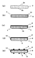
図1(a),(b)に示すように、両面電極型の太陽電池素子1は、光が入射する受光面である第1面2aとこれに対向する裏面である第2面2bとを有する半導体基板2と、この半導体基板2の第1面2a上に設けられたバスバー電極3およびフィンガー電極4と、第2面2b上に設けられた集電電極5と、出力取出電極6と、を有する。
<< Double-sided electrode type solar cell element >>
As shown in FIGS. 1A and 1B, a double-sided electrode type
半導体基板2は、例えば単結晶シリコンまたは多結晶シリコンなどから成るシリコンウエハなどから構成され、例えば1辺が150〜160mm程度の矩形の平板状をなす。また、半導体基板2は一導電型の半導体層と逆導電型の半導体層とを有する。すなわち、このシリコンウエハの内部には、p型シリコンの層とn型シリコンの層とがあり、これらの接合(pn接合)部が形成されている。このシリコンウエハは後で説明するように、例えば、一導電型のバルク層と逆導電型の表面層とでpn接合部が形成される。このように、太陽電池素子1は、主に一導電型の半導体基板2を備え、この半導体基板2の少なくとも一方主面に逆導電型の半導体層が形成されている。
The
第1面2a上に形成される電極は、幅1mm〜3mm程度の幅の広いバスバー電極3と、バスバー電極3に対して略垂直に交わるように設けられており、幅50〜200μm程度の細いフィンガー電極4とから成る。このようなバスバー電極3およびフィンガー電極4の厚みは、10〜20μm程度である。また、第1面2aの全面には、予め反射防止膜8を形成しておくことが望ましい。
The electrodes formed on the
第2面2b上に形成される電極は、集電電極5および出力取出電極6である。この出力取出電極6の厚みは10μm〜20μm程度であり、幅は3.5mm〜7mm程度である。また、集電電極5の厚みは15μm〜50μm程度である。
The electrodes formed on the
このようなフィンガー電極4および集電電極5は、発生したキャリアを集電する役割を有し、バスバー電極3および出力取出電極6は、フィンガー電極4および集電電極5で集めたキャリア(電力)を集め、外部に出力する役割を有している。
The
次に、太陽電池素子1の作用について説明する。太陽電池素子1の第1面2a側から光が入射すると、この光は半導体基板2で吸収・光電変換(電子−正孔対(電子キャリアおよび正孔キャリア)が生成される)。この光励起起源の電子キャリアおよび正孔キャリア(光生成キャリア)が上述のpn接合の働きにより、太陽電池素子1の第1面2aおよび第2面2bのそれぞれに設けられた電極に集められ、両電極間に電位差が生ずる。
Next, the operation of the
<<太陽電池素子の製造方法>>
次に、このタイプの太陽電池素子1の製造方法の一例について説明する。
<< Method for Manufacturing Solar Cell Element >>
Next, an example of a method for manufacturing this type of
まず、図2(a)に示すように、一導電型の単結晶または多結晶のシリコンから成る半導体基板2を準備する。この半導体基板2は、例えばボロン(B)などのp型の導電型を呈する比抵抗0.2〜2.0Ω・cm程度のp型基板が好適に用いられる。なお、場合によっては一導電型としてn型を呈する基板を用いてもよいが、以下、p型基板を例にとり説明する。
First, as shown in FIG. 2A, a
半導体基板2が単結晶シリコンウエハの場合は、チョクラルスキー法などの引き上げ法などによって作製される。半導体基板2が多結晶シリコンウエハの場合は鋳造法などによって作製される。
When the
多結晶シリコンウエハは大量生産が可能であり、製造コスト面で単結晶シリコンウエハよりも有利であるので、以下、半導体基板2として多結晶シリコンを用いた例を説明する。
Since a polycrystalline silicon wafer can be mass-produced and is more advantageous than a single crystal silicon wafer in terms of manufacturing cost, an example in which polycrystalline silicon is used as the
多結晶シリコンのインゴットは、例えばワイヤーソーなどを用いて350μm以下、より好ましくは200μm以下の厚みにスライスして半導体基板2とする。なお、半導体基板2の表面に付着したスライス時の汚染層を清浄化するために、表面をNaOH、KOH、またはフッ酸とフッ硝酸の混合溶液などを用いて、ごく微量エッチングすることが望ましい。
The polycrystalline silicon ingot is sliced to a thickness of 350 μm or less, more preferably 200 μm or less, using a wire saw, for example, to form the
次に、半導体基板2の第1面2a側に、ドライエッチング方法またはウェットエッチング方法などを用いて、RIE(リアクティブイオンエッチング)装置などを用いて光反射率低減機能を有する凹凸(粗面化)構造を形成するのが好ましい。
Next, on the
その後、図2(b)に示すように、半導体基板2の表面全体にn型層9を形成する。n型化ドーピング元素としてはP(リン)を用いることが好ましく、シート抵抗が30〜300Ω/□程度のn型とする。これによって、n型層9とp型バルク領域10との間にpn接合部が形成される。
Thereafter, as shown in FIG. 2B, an n-
n型層9の形成は、例えば、半導体基板2を700〜900℃程度に昇温して、この温度に維持しながら、拡散源22として用いるガス状態にしたPOCl3(オキシ塩化リン)雰囲気中で、気相熱拡散法などによって20〜40分程度処理することにより行う。これにより、n型層9は0.2〜0.7μm程度の厚みに形成される。この際に、半導体基板2の表面全体にリンガラスが形成される。そこで、このリンガラスを除去するために、この半導体基板2をフッ酸に浸漬し、洗浄乾燥することが必要になる。
The n-
その後、図2(c)に示すように、半導体基板2の第2面2bの端面外周部に形成されているn型層9の部分を除去して、この除去部7によりpn分離を行う。このn型層9の部分の除去は、アルミナまたは酸化シリコンの粒子を高圧でシリコンウエハの第2面2bの端面外周部に吹きつけるサンドブラスト法、またはYAG(イットリウム・アルミニウム・ガーネット)レーザーなどにより、pn接合部に達する分離溝を形成することで行う。これにより、pn分離を行うことができる。
After that, as shown in FIG. 2C, the portion of the n-
さらに、このpn分離後に、図2(c)に示すように、第1面2aに反射防止膜8を形成する。反射防止膜8の材料としては、SiNx膜(ただし、組成比「x」はSi3N4ストイキオメトリを中心にして幅がある。)、TiO2膜、SiO2膜、MgO膜、ITO膜、SnO2膜またはZnO膜などを用いることができる。反射防止膜8の厚さは、材料によって適宜選択されて、適当な入射光に対して無反射条件を実現できるようにする。例えば半導体基板2の場合、屈折率は1.8〜2.3程度、厚み500〜1200Å程度にすればよい。反射防止膜8の製法としては、PECVD法、蒸着法またはスパッタ法な
どを用いることができる。
Further, after this pn separation, an
次に図2(d)に示すように、半導体基板2の第2面2b側に集電電極5を形成する。集電電極5は、アルミニウムを主成分とするペーストを第2面2bの外周辺部1〜5mm程度を除いて、第2面2bの略全面に塗布することで形成する。この塗布法としては、スクリーン印刷法などを用いることができる。この集電電極5の形成に用いるペーストは、アルミニウム粉末と有機ビヒクルなどからなるものであり、これを塗布した後、温度700〜850℃程度で熱処理(焼成)してアルミニウムを半導体基板2に焼き付ける。このアルミニウムペーストを印刷し、焼成する。これにより、p型不純物であるアルミニウムを半導体基板2の塗布部分に高濃度に拡散させることができ、裏面側にも形成されているn型層をp+型とすることができる。
Next, as shown in FIG. 2D, the
次に図2(e)に示すように、第1面2aの電極(バスバー電極3およびフィンガー電極4)と第2面2bの出力取出電極6を形成する。
Next, as shown in FIG. 2E, electrodes (
このようにして、第2面2bの出力取出電極6は、導電ペーストを塗布することにより形成することができる。
Thus, the
以下に、上記導電ペーストとして、コーティングフィラーを用いる場合および混合フィラーを用いる場合のそれぞれについて説明する。 Hereinafter, the case where a coating filler is used and the case where a mixed filler is used as the conductive paste will be described.
<コーティングフィラーを用いた例>
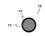
銀を表面にコーティングした銅フィラーを用いる例について説明する。図3に示すように、銅フィラー13は、銀層15を銅本体14の表面にコーティングしている。ここで、銅フィラー13は、例えば直径0.1〜10μm程度の球状であるが、この形状に限定されるものではなく、例えば断面が楕円となるラグビーボール状、または角部を持つ多面体形状でもよい。なお、銅本体14の表面には微細な凹凸が形成されていてもよい。この銅フィラー14の材料としては、純度99.9質量%以上の銅とすると好適である。特に、太陽電池素子1の直列抵抗成分を低下させるために、抵抗の低い無酸素銅をより好適に用いることができる。
<Example using coating filler>
The example using the copper filler which coated silver on the surface is demonstrated. As shown in FIG. 3, the
銅本体14の表面には、銀層15を0.005μm〜0.1μm程度の厚みでコーティングする。このコーティングは、均一の厚みでコーティングできるため、置換法で行うことが望ましい。このコーティングする銀層15は、99.9質量%以上の純度を持ったものが望ましい。
The surface of the
第2面2bの出力取出電極6を形成する導電ペーストは、銀層15を表面にコーティングした銅フィラー13の多数と有機ビヒクルとガラスフリットとを、銀層15を表面にコーティングした銅フィラー13の多数からなる100質量部に対して、有機ビヒクルを10〜20質量部とし、ガラスフリットを5〜15質量部としたものを添加したものである。さらに、テレピネオールなどの溶剤を用いて、50〜200Pa・sの程度の粘度に調節したものを用いることができる。
The conductive paste forming the
塗布法としては、スクリーン印刷法などを用いることができ、塗布後所定の温度で溶剤を蒸散させて乾燥させることが好ましい。 As the coating method, a screen printing method or the like can be used, and it is preferable that the solvent is evaporated and dried at a predetermined temperature after coating.
集電電極5上に銀層15を表面にコーティングした銅フィラー13を含有する導電ペーストを塗布後、焼成炉内にて最高温度が500〜650℃で数十秒〜数十分程度焼成することにより裏面電極(集電電極5、出力取出電極6)を形成する。銀層15を表面にコーティングした銅フィラー13を含有する導電ペーストの焼成においては、銅フィラー13
の酸化を抑制するため、炉内のピーク温度付近の位置の酸素濃度が100ppm〜500ppmになるように、窒素ガスなど不活性ガスを炉内部に導入することが望ましい。
After applying a conductive paste containing a
In order to suppress the oxidation, it is desirable to introduce an inert gas such as nitrogen gas into the furnace so that the oxygen concentration near the peak temperature in the furnace becomes 100 ppm to 500 ppm.
通常、太陽電池素子1の出力取出電極6の形成において、銀を主成分とする導電ペーストを用いた場合、アルミニウムを主成分とする集電電極5と出力取出電極6の接合強度が弱い。なぜなら、アルミニウムを主成分とする集電電極5のアルミニウムの表面酸化により充分な接着力が得られないからである。
Usually, in the formation of the
このため、太陽電池素子1の完成後の太陽電池モジュール製造工程において、太陽電池素子同士を繋ぐための接続タブの出力取出電極6へのハンダ付けなどで、出力取出電極6の剥離が発生する心配があった。そこで、この対策として、集電電極5を形成するためのアルミニウムを主成分とするペーストを第2面2bに塗布する際、出力取出電極6が配置される箇所に、部分的にアルミニウムを主成分とするペーストが塗布されない部分を故意に作製していた。これにより、半導体基板2と出力取出電極6が直接接する部分を作製し、この部分の強固な接合強度を利用して、後工程での出力取出電極6の剥離を抑制していた。
For this reason, in the solar cell module manufacturing process after the completion of the
しかしながら、このような構造にすると、p型シリコンと銀電極はオーミックコンタクト性が悪いため、この部分での光発生キャリアの取り出しができないので、ロスが発生し太陽電池素子の光電変換効率低下の一因となっていた。 However, with such a structure, the p-type silicon and the silver electrode have poor ohmic contact properties, so that the photogenerated carriers cannot be taken out at this portion, so that loss occurs and the photoelectric conversion efficiency of the solar cell element decreases. It was a cause.
これに対して、本実施形態の太陽電池素子においては、第2面2bの出力取出電極6は、銀層15を表面にコーティングした銅フィラー13を含有する導電ペーストを塗布することにより形成する。このため、集電電極5の主成分であるアルミニウムと銅の接合強度を、上述の太陽電池モジュール工程においても、出力取出電極6の剥離の心配が無いほど十分強固にすることが可能になる。これにより、信頼性を向上させることができる。また、集電電極5を形成するときに、部分的にアルミニウムを主成分とするペーストが塗布されない部分を設ける必要が無い。これにより、半導体基板2と出力取出電極6が直接接する部分を無くすことができ、太陽電池素子の光電変換効率を向上させることが可能となる。さらに、導電ペーストにおける高価な銀の使用量を減らせる。
On the other hand, in the solar cell element of the present embodiment, the
また、第2面2b側の電極形成の工程は、上述のようにアルミニウムペーストを塗布・焼成して集電電極5を形成し、その後、銀を表面にコーティングした銅フィラーを多数含有する導電ペーストを塗布・焼成し出力取出電極6を形成して、焼成工程を別々にしてもよい。あるいは、アルミニウムペーストを塗布・乾燥した後、銀を表面にコーティングした銅フィラーを多数含有する導電ペーストを塗布し、両者を同時に焼成してもよい。
In addition, the electrode forming step on the
次に、半導体基板2の第1面2aの電極(バスバー電極3とフィンガー電極4)の形成は、同様にして銀層15を表面にコーティングした銅フィラー13を含有する導電ペーストを用いることで可能である。すなわち、反射防止膜8の上にバスバー電極3とフィンガー電極4を、銀層15を表面にコーティングした銅フィラー13を含有する導電ペーストで直接塗布し焼き付けて形成する。この結果、第1面2aの電極の焼成時に電極中のガラス成分が反射防止膜8を突き破ることになり、この電極の直下はn型層9になる。これにより、第1面2aのバスバー電極3およびフィンガー電極4と、n型層9とを電気的に接触させることができる。第1面2aの電極にも、銀層15を表面にコーティングした銅フィラー13を含有する導電ペーストを用いると製造コストの面でよい。
Next, the electrodes (
また、第1面2aの電極を通常の銀を主成分とした導電ペーストで形成することも可能である。銀を主成分とした導電ペーストは、銀からなる金属粉末銀100質量部に対して、有機ビヒクルを5〜30質量部、およびガラスフリットを0.1〜10質量部、それぞ
れを添加して、ペースト状にした銀ペーストを所定の電極形状に塗布し、最高温度が600〜850℃で数十秒〜数十分程度焼成することにより形成可能である。塗布法としては、スクリーン印刷法などの周知の方法を用いることができる。
Moreover, it is also possible to form the electrode of the
<混合フィラーを用いた電極形成>
出力取出電極6を形成するための導電ペーストは、例えば、多数の銀フィラーと多数の銅フィラーと有機ビヒクルとガラスフリットを銀と銅の合計100質量部に対してそれぞれ5〜30質量部、0.1〜15質量部配合、混練し、溶剤を用いて、50〜200Pa・sの程度の粘度に調節したものを用いてもよい。
<Electrode formation using mixed filler>
The conductive paste for forming the
この混練は、多数の銀フィラーと有機ビヒクルとガラスフリットを上記の割合で混練しペースト状にする。この作業と並行して多数の銅フィラーと有機ビヒクルとガラスフリットを上記の割合で混練しペースト状にする。そして、これら2つのペーストを予め用意しておき、これらペーストを所定の割合で混練し、その後溶剤を用いて所定の粘度の調整する。これにより、銀と銅のフィラーがより均一に混ざり合うため好ましい。 In this kneading, a large number of silver fillers, an organic vehicle, and glass frit are kneaded in the above ratio to form a paste. In parallel with this operation, a large number of copper fillers, organic vehicle, and glass frit are kneaded at the above ratios to form a paste. Then, these two pastes are prepared in advance, these pastes are kneaded at a predetermined ratio, and then a predetermined viscosity is adjusted using a solvent. Thereby, since the filler of silver and copper mixes more uniformly, it is preferable.
塗布法としては、スクリーン印刷法などを用いることができ、塗布後所定の温度で溶剤を蒸散させて乾燥させることが好ましい。 As the coating method, a screen printing method or the like can be used, and it is preferable that the solvent is evaporated and dried at a predetermined temperature after coating.
集電電極5上に銀と銅を含有する導電ペーストを塗布、乾燥後、焼成炉内にて最高温度が500〜650℃で数十秒〜数十分程度焼成することにより出力取出電極6を形成する。この銀と銅を含有する導電ペーストの焼成においては、含有している銅フィラーの酸化を防止するため、炉内のピーク温度付近の位置の酸素濃度が500ppm未満になるように、窒素ガスなど不活性ガスを炉内部に導入することが望ましい。
After applying and drying a conductive paste containing silver and copper on the collecting
通常、太陽電池素子の出力取出電極6形成において、銀のみを主成分とする導電ペーストを用いた場合、アルミニウムを主成分とする集電電極5と出力取出電極6の接合強度が弱くなる。このため該太陽電池素子の完成後の太陽電池モジュール製造工程において、太陽電池素子同士を繋ぐための接続タブの出力取出電極6へのハンダ付けなどで、出力取出電極6の剥離が発生する心配があった。このための対策として、集電電極5を形成するためのアルミニウムを主成分とするペーストを第2面2bに塗布するときに、出力取出電極6が配置されるところに、部分的にアルミニウムを主成分とするペーストが塗布されない部分を故意に造っていた。これにより半導体基板2と出力取出電極6が直接接する部分を作製し、この部分の強固な接合強度を利用して、後工程での出力取出電極6の剥離を防止していた。
Usually, in the formation of the
しかしながらこのような構造にすると、p型シリコンと銀電極はオーミックコンタクト性が悪いため、この部分での光発生キャリアの取り出しができないので、ロスが発生し太陽電池素子の光電変換効率低下の一因となっていた。 However, with such a structure, the p-type silicon and the silver electrode have poor ohmic contact properties, so that the photogenerated carriers cannot be taken out at this portion, causing a loss and a factor in reducing the photoelectric conversion efficiency of the solar cell element. It was.
これに対し本発明に係る太陽電池素子においては、第2面2bの出力取出電極6は、銀と銅を含有する導電ペーストを塗布することにより形成するため、集電電極5の主成分であるアルミニウムと銅の接合強度を、上述の太陽電池モジュール工程においても出力取出電極6の剥離の心配が無いほど十分強固にすることが可能となり、その信頼性を向上させることができる。
On the other hand, in the solar cell element according to the present invention, the
また、集電電極5を形成するときに、部分的にアルミニウムを主成分とするペーストが塗布されない部分を故意に造る必要が無く、半導体基板2と出力取出電極6が直接接する部分を無くすことができ、太陽電池素子の光電変換効率を向上させることが可能となる。さらに導電ペーストにおける銀の使用量を減らせるため、製造コストの面でよい。
Further, when forming the
さらに、発明者らが繰り返し行ったテストの結果では、この導電ペーストに含有される銀と銅の質量比は、銀:銅=2:8〜7:3の範囲であることが望ましい。 Furthermore, as a result of tests repeatedly conducted by the inventors, it is desirable that the mass ratio of silver and copper contained in the conductive paste is in the range of silver: copper = 2: 8 to 7: 3.
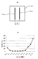
図4(a)は、半導体基板2上に上記のようにアルミニウムを主成分とするペーストを、スクリーン印刷法を用いて第2面2bの略全面に塗布、焼成することで形成した集電電極5上に、銀と銅の質量比を変えた導電ペーストをスクリーン印刷法を用いて所定の電極パターンに塗布し、最高温度約600℃程度で焼成することで形成した出力取出電極6の集電電極5との接合強度を測定した結果である。
FIG. 4A shows a collector electrode formed by applying and baking a paste mainly composed of aluminum as described above on the
図4(a)に示すように、第2面2bの集電極5上の出力取出電極6においては、銀と銅の質量比である銀:銅が、10:0から8:2の範囲では接合強度は銅とアルミニウムの合金の生成が不充分のため弱く、銀:銅が10:0から7:3までは、銅とアルミニウムの合金の生成が増加するために急激な上昇がみられるものと考えられる。さらに銀:銅=2:8から0:10の範囲では、酸化した銅の割合が大きくなるため、銀:銅=2:8から0:10まで急激に低下するものと思われる。
As shown in FIG. 4A, in the
またこの第2面2b側の電極形成の工程は、上述のようにアルミニウムペーストを塗布・焼成して集電電極5を形成し、その後銀と銅を含有する導電ペーストを塗布・焼成して出力取出電極6を形成して焼成工程を別々にしても良いし、アルミニウムペーストを塗布・乾燥した後、銀を表面にコーティングした銅フィラーを含有する導電ペーストを塗布し、両者を同時に焼成してもよい。
Further, in the electrode forming step on the
次に半導体基板2の第1面2aの電極(バスバー電極3とフィンガー電極4)を形成する。このバスバー電極3とフィンガー電極4の形成においても、本発明に係る銀と銅を含有する導電ペーストを塗布することにより形成することが望ましい。
Next, electrodes (
バスバー電極3とフィンガー電極4を形成するための導電ペーストは、例えば銀のフィラーと銅のフィラーと有機ビヒクルとガラスフリットを銀と銅の合計100質量部に対してそれぞれ5〜30質量部、0.1〜15質量部配合、混練し、溶剤を用いて、50〜200Pa・sの程度の粘度に調節したものである。
The conductive paste for forming the
塗布法としては、スクリーン印刷法などを用いることができ、塗布後所定の温度で溶剤を蒸散させて乾燥させることが好ましい。 As the coating method, a screen printing method or the like can be used, and it is preferable that the solvent is evaporated and dried at a predetermined temperature after coating.
バスバー電極3とフィンガー電極4を形成するための導電ペーストを塗布、乾燥後、焼成炉内にて最高温度が500〜650℃で数十秒〜数十分程度焼成することによりバスバー電極3とフィンガー電極4を形成する。この銀と銅を含有する導電ペーストの焼成においては、含有している銅フィラーの酸化を防止するため、炉内のピーク温度付近の位置の酸素濃度が500ppm未満になるように、窒素ガスなど不活性ガスを炉内部に導入することが望ましい。
After applying and drying a conductive paste for forming the
また、バスバー電極3とフィンガー電極4を形成するための導電ペーストの焼成は、上述の出力取出電極6を形成するための導電ペーストの焼成と同時に行うことが、別々に焼成するよりもバスバー電極3、フィンガー電極4と出力取出電極6とも焼成が1回になり、銅の酸化を抑制できるため望ましい。
In addition, the baking of the conductive paste for forming the
このように反射防止膜8の上にバスバー電極3とフィンガー電極4の所定形状に銀と銅を含有する導電ペーストを直接塗布し、焼成することによって第1面のバスバー電極3、フィンガー電極4とn型層9を電気的に接触させる。
In this way, the conductive paste containing silver and copper is directly applied to the predetermined shape of the
これにより銀と銅の両方の粒子がn型層9と接触することにより、オーミックコンタクト性が改善され、完成した太陽電池素子の光電変換効率を向上させることが可能となる。さらに銀と銅を含有する導電ペーストを用いることにより、製造コストの面で望ましい。
As a result, both silver and copper particles come into contact with the n-
また、銀と銅を含有する導電ペーストを、バスバー電極3とフィンガー電極4の形成に用いる場合、発明者らが繰り返し行ったテストの結果では、図4(b)に示すように、導電ペーストに含有される銀と銅の質量比は、銀:銅=9:1〜3:7の範囲であることが望ましい。
In addition, when a conductive paste containing silver and copper is used for forming the
図4(b)は、半導体基板2上に反射防止膜として厚さ700〜900Å程度の窒化シリコン膜をプラズマCVD装置を用いて成膜し、この反射防止膜上に銀と銅の質量比を変えた導電ペーストをスクリーン印刷法を用いて所定の電極パターンに塗布し、最高温度約600℃程度で焼成することで形成した出力取出電極6の集電電極5との接合強度を測定した結果である。
In FIG. 4B, a silicon nitride film having a thickness of about 700 to 900 mm is formed as an antireflection film on the
図4(b)に示すように、第1面2aのバスバー電極3とフィンガー電極4においては、銀と銅の質量比である銀:銅が、10:0では接合強度はガラスフリットのシリコンへの浸透が不充分のため弱く、銀:銅が10:0から9:1の範囲では銅によりガラスフリットのシリコンへの浸透が促進されるために急激な上昇がみられるものと考えられる。さらに銀:銅=3:7から0:10の範囲では、酸化した銅の割合が大きくなるため、銀:銅=3:7から0:10まで急激に低下するものと思われる。
As shown in FIG. 4B, in the
図5(a)は、この電極とn型層9との接合部の抵抗を測定するために作製したテストピースの平面図である。これは、約150mm角のp型多結晶シリコン基板2の表面に、リンをシート抵抗が50〜100Ω/□程度になるように拡散させてn型層9とし、そのほぼ中央部に約50mmの間隔Dを開けて、長さ約130mm、幅約2mmで銀と銅の質量比を変えた導電ペーストをスクリーン印刷し、その後焼成して、電極12a,12bを形成したものである。焼成後、電極12a,12bのそれぞれの厚みは、約13μmであった。その後に、電極12a,12b間の抵抗を測定した。
FIG. 5A is a plan view of a test piece prepared for measuring the resistance of the junction between this electrode and the n-
図5(b)は、使用した導電ペーストに含有される銀と銅の質量比と、導電ペーストの焼成後の抵抗値との関係を示すグラフである。 FIG.5 (b) is a graph which shows the relationship between the mass ratio of silver and copper contained in the used electrically conductive paste, and the resistance value after baking of an electrically conductive paste.
これより明確なように、銀と銅の質量比が、9:1〜3:7の範囲では、抵抗値は100mΩ未満の小さい値であり、オーミックコンタクト性は良好であるが、この範囲外では急激に上昇していることがわかる。 As is clear from this, when the mass ratio of silver and copper is in the range of 9: 1 to 3: 7, the resistance value is a small value of less than 100 mΩ and the ohmic contact property is good, but outside this range, It turns out that it is rising rapidly.
その理由は、銀と銅の質量比が0:10〜2:8の範囲では酸化した銅の割合が大きくなるための影響と考えられ、また、銀と銅の質量比10:0では銅によるオーミックコンタクト性の改善の効果が見られないためと考えられる。 The reason for this is thought to be the effect of increasing the proportion of oxidized copper when the mass ratio of silver to copper is in the range of 0:10 to 2: 8, and also due to copper at the mass ratio of silver to copper of 10: 0. This is probably because the effect of improving the ohmic contact property is not seen.
<<バックコンタクト型太陽電池素子>>
次に、バックコンタクト型の太陽電池素子について説明する。
<< Back contact solar cell element >>
Next, a back contact type solar cell element will be described.
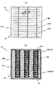
図6,7に示すように、本実施形態の太陽電池素子21は、太陽光の受光面となる第1面21aと、その裏面となる第2面21bとを含み、第1面21aと第2面21bとを貫通する複数の貫通孔28を有する半導体基板25から成る。
As shown in FIGS. 6 and 7, the
また、この貫通孔28の内部には導体である導電性充填材Gが充填され、貫通孔電極2
2bが形成されている。
Further, the inside of the through
2b is formed.
太陽電池素子21の第1面21a上に形成された受光面電極22aは、図6(a)に示すように、複数本の直線細線状の電極がほぼ等間隔に設けられ、さらに各々1本の受光面電極22aには貫通孔電極22bをほぼ同じ位置にそれぞれ1〜5個程度接続されている。このように、一本の受光面電極22aに一つ以上の貫通孔電極22bを備えることになり、一つの貫通孔電極22bにおける光電流の密度を小さくすることができ、太陽電池素子の抵抗成分を下げることができる。
As shown in FIG. 6 (a), the light receiving
この第1面21aの電極に対応する第2面21bに形成された電極の形状は、図6(b)に示すように、まず貫通孔電極22bの直下に、これと電気的に接続された矩形状の第1電極22cが複数個、一直線上にほぼ一定間隔で配置される。この第1電極22cの一つには、貫通孔電極22bが一つまたは複数個、接続されている。
The shape of the electrode formed on the
さらに、第2面21bには、第1電極22cとは異なる極性を持った第2電極23が設けられる。この第2電極23は集電電極23aと出力取出電極23bから成る。
Further, the
すなわち、上記の直線状に配置された第1電極22cとその周辺部以外の部分に、集電電極23aが配置され、この集電電極23a上に出力取出電極23bが形成される。
That is, the
出力取出電極23bは、各々集電電極23a上の対向する位置に設けられる。この対向する出力取出電極23bの2つの領域は、第3電極24で電気的に接続されている。
The
半導体基板25は一導電型を有し、この半導体基板25の第1面21aおよび裏面1bには、図7(a),(b)に示すように、半導体基板25の導電型と異なる逆導電型半導体層26(第1逆導電型層26a、第3逆導電型層26c)を有する。また半導体基板25の電極用貫通孔28の内面には、第2逆導電型層26bが設けられている。
The
一導電型を示す半導体基板25としてp型のシリコン基板を使用する場合、このような逆導電型層26はn型となり、例えばリンなどのn型不純物を半導体基板25表面と電極用貫通孔28の内面に拡散することで形成される。
When a p-type silicon substrate is used as the
また図7(a),(b)において、集電電極23aの電極材料として主としてアルミニウムが用いられた場合、これを塗布、焼成して集電電極23aを形成する際に、高濃度ドープ層30を同時に形成することができる。すなわち集電電極23aは、高濃度ドープ層30上に形成されることになる。これにより、半導体基板25中で生成されたキャリアが効率よく集電される。ここで、高濃度とは半導体基板25における一導電型不純物の濃度よりも不純物濃度が大きいことを意味する。
7A and 7B, when aluminum is mainly used as the electrode material of the
このように、本実施形態の太陽電池素子21では、その第1面21aおよび貫通孔28内部には、受光面電極22aと貫通孔電極22bが設けられ、その第2面21b上においては、逆導電型半導体層26上に第1電極22cが設けられ、また逆導電型半導体層26の非形成部には、第2電極23として集電電極23aと出力取出電極23bが設けられる。
As described above, in the
また、半導体基板25の一導電型(例えばp型)と逆導電型層(例えばn型)を電気的に分離(pn分離)するため、図4(a)に示すように、第1電極22cを取り囲むように、その周辺部に分離溝29aが設けられ、さらに半導体基板25の裏面21bの外周端部に分離溝29bが設けられる。
Further, in order to electrically isolate (pn-separate) one conductivity type (for example, p-type) and reverse conductivity type layer (for example, n-type) of the
本実施形態の集電電極23a上の出力取出電極23bは、銀を表面にコーティングした銅フィラーを多数含有する導電ペーストをプリント印刷法などにより塗布し、焼成することで形成される。これにより、集電電極2と出力取出電極23bの接合強度を向上することができ、より信頼性の高い太陽電池素子21を提供することが可能となる。
The
<<バックコンタクト型太陽電池素子の製造方法>>
次に、本実施形態の太陽電池素子21の製造方法について説明する。
<< Method for Manufacturing Back-Contact Solar Cell Element >>
Next, the manufacturing method of the
<半導体基板の準備工程>
まず、一導電型を示す半導体基板25として、例えばボロンなどがドープされたp型のシリコン基板を準備する。このシリコン基板は、シリコンインゴットから切り出された単結晶シリコン基板や多結晶シリコン基板からなるシリコン基板を用いればよく、シリコン基板の大きさは例えば一辺140〜180mm程度の正方形または矩形で、その厚みは150μm〜300μm程度にすればよい。
<Preparation process of semiconductor substrate>
First, as a
<貫通孔の形成工程>
次に、半導体基板25の第1面21aと裏面21bとの間に貫通孔28を形成する。この貫通孔28は、機械的ドリル、ウォータージェットあるいはレーザー装置等を用いて、例えば半導体基板25の第2面21b側から第1面21a側に向けて形成される。特に、貫通孔28の形成時またはその形成後のマイクロクラックの発生抑制のために、レーザーなどが好適に用いられる。このようなレーザーとしては、例えばエキシマレーザー、YAG(イットリウム・アルミニウム・ガーネット)レーザーまたはYVO4(イットリウム・バナデイト)レーザー等を使用することができる。なお形成される貫通孔28の直径は20〜50μm程度が好ましい。
<Through-hole formation process>
Next, a through
<表面エッチング>
貫通孔28を設けた半導体基板25を、水酸化ナトリウムが10〜30質量%程度で、60〜90℃の水酸化ナトリウム水溶液で5〜20μm程度エッチングする。これにより、貫通孔28内部の側面もエッチングされ、その表面が粗面化される。この粗面化により導電性充填材Gとの接触面積を増加させることができ、両者の接着強度を向上せせることが可能となる。また、このエッチングにより、上述のシリコンインゴットから切り出し時に生じたダメージ層をも除去することができる。さらに、第1面21aも粗面化でき、太陽電池素子21に入射した光の反射を抑えることができ、その光電変換効率をより向上させることができる。
<Surface etching>
The
<逆導電型層の形成工程>
次に、半導体基板25の表面に逆導電型層26を形成する。逆導電型層26を形成するためのn型化ドーピング元素としてはリン(P)を用い、シート抵抗が60〜300Ω/□程度のn+型とする。これにより、逆導電型層26とp型バルク領域との間にpn接合部が形成される。
<Reverse conductivity type layer formation process>
Next, the reverse
さらに、この逆導電型層26に例えば気相拡散法が用いられた場合、半導体基板25の両面および貫通孔28内壁に、同時に逆導電型層26を形成することができる。この貫通孔28の内壁に逆導電型層26bが形成されたことにより、この部分のリーク電流を抑えることが可能になる。
Furthermore, for example, when the vapor phase diffusion method is used for the reverse
<反射防止膜の形成工程>
次に、第1逆導電型層26aの上に、反射防止膜27を形成することが好ましい。この反射防止膜27の材料としては、窒化珪素膜または酸化チタン膜などを用いることができる。反射防止膜27の形成方法としては、PECVD法、蒸着法またはスパッタ法などを
用いることができる。
<Antireflection film formation process>
Next, it is preferable to form the
<受光面電極と貫通孔電極の形成工程>
次に、半導体基板25に、受光面電極22aと貫通孔電極22bを形成する。これらの電極は、半導体基板5の第1面1cにスクリーン印刷法などの塗布法を用いて銀を表面にコーティングした銅フィラーを多数含有する導電ペーストを塗布し、焼成することにより形成される。
<Step of forming light-receiving surface electrode and through-hole electrode>
Next, the light receiving
また、通常の銀を主成分とする導電ペーストを用いて、これを塗布、焼成することで受光面電極22aと貫通孔電極22bを形成してもよい。
Moreover, you may form the light-receiving
<集電電極の形成工程>
次に、半導体基板25の裏面21b上に、集電電極23aを形成する。これは、スクリーン印刷法を用いて、半導体基板25の裏面21b上にアルミニウムを主成分とする導電性ペーストを所定の電極形状に塗布し、その後、上述のように焼成することにより集電電極23aを形成する。また、これにより一導電型半導体不純物が高濃度に拡散された高濃度ドープ層30を形成することも可能となる。
<Formation process of current collecting electrode>
Next, the
<第1電極と出力取出電極と第3電極の形成工程>
次に、半導体基板25の第2面21b上に第1電極22cと出力取出電極23bと第3電極24とを形成する。本実施形態の太陽電池素子21においては、第1電極22cと出力取出電極23bと第3電極24を、両面電極型太陽電池素子で説明したように、銀層を表面にコーティングした銅フィラーを多数含有する導電ペーストを用いて行う。
<Formation process of 1st electrode, output extraction electrode, and 3rd electrode>
Next, the
すなわちスクリーン印刷法を用いて、半導体基板25の裏面21bに、例えば、図1(a)に示されたような第1電極22cと出力取出電極23bと第3電極24の形状に、図3に示すように、銀層15を表面にコーティングした銅フィラー13を多数含有する導電ペーストを塗布し、その後上述のように焼成することで第1電極2cと出力取出電極3bと第3電極4とを形成する。
That is, by using the screen printing method, the shape of the
<pn分離工程>
例えば、上述の気相拡散法を用いて逆導電型層の形成を行った場合、半導体基板25の両面および貫通孔28内壁に、同時に逆導電型層26が形成される。このため、半導体基板25の第1面21aと裏面21bの逆導電型層を分離(pn分離)する。このpn分離は、裏面21bの周辺部のみに酸化珪素やアルミナなどの粉末を高圧で吹きつけ裏面21bの周辺部の逆導電型層を削り取るブラスト加工法や裏面21bの周辺端部に分離溝29bを形成するレーザー加工法で可能である。
<Pn separation step>
For example, when the reverse conductivity type layer is formed using the above-mentioned vapor phase diffusion method, the reverse
次に、第1電極22c周囲部分のpn分離を行う。第1電極22cの周辺部、すなわち第1電極22cと集電電極23a、第3電極24の間にできた半導体基板25の部分にYAGレーザー(波長1064nm)などを用いてレーザー光を照射し、矩形状に分離溝29aを形成することで行う。
Next, pn separation is performed around the
以上により、両面電極型太陽電池素子と同様な効果を奏することができるバックコンタクト型太陽電池素子が完成する。なお、バックコンタクト型太陽電池素子は上述の太陽電池素子に限定されるものではなく、貫通孔を形成しないIBC(Interdigitated Back Contact)構造のバックコンタクト型太陽電池素子においても応用可能である。 As described above, a back contact type solar cell element capable of producing the same effect as the double-sided electrode type solar cell element is completed. The back contact solar cell element is not limited to the solar cell element described above, and can be applied to a back contact solar cell element having an IBC (Interdigitated Back Contact) structure in which no through hole is formed.
<<タイプ2について>>
タイプ2の場合については詳しく述べなかったが、例えば、n型のシリコン基板の一方
主面上に、i型およびp型のアモルファスシリコン層をこの順で製膜し、他方主面上に例えばi型およびn型のアモルファスシリコン層をこの順で製膜して、全体として1つの半導体基板を構成するような場合、いわゆるヘテロ構造を有する太陽電池素子に対しても、本実施形態を適用することは可能であり、タイプ1と同様な作用・効果を期待することができる。
<< About
Although the case of
以下に、両面電極型太陽電池素子の実施例について説明する。 Below, the Example of a double-sided electrode type solar cell element is described.
<実施品1の作製>
まず、鋳造法で作製した多結晶シリコンからなる半導体基板2を準備した。この半導体基板2は、p型不純物であるボロン(B)を1×10¹⁶〜1018atoms/cm3程度含有したものであり、その大きさは約150mm角、厚さは約0.2mm程度のものである。
<Preparation of Example 1>
First, a
この半導体基板2の表面を清浄化するために、その表面を濃度が20%程度の水酸化ナトリウム水溶液でごく微量エッチングし洗浄した。
In order to clean the surface of the
次に、光入射面となる半導体基板2の第1面2a側に、RIE(リアクティブイオンエッチング)装置を用いて、光反射率低減機能を有する微細な凹凸(粗面化)構造を形成した。
Next, a fine unevenness (roughening) structure having a light reflectance reduction function was formed on the
その後、半導体基板2の表面全体にn型層9を形成した。n型化ドーピング元素としてはリン(P)を用い、シート抵抗が50〜100Ω/□程度のn型とした。これによって、上述のn型層9とp型バルク領域との間にpn接合部が形成された。
Thereafter, the n-
このn型層9の形成は、次のようにして行った。半導体基板2を700〜900℃程度に昇温して維持しながら、拡散源としてガス状態にしたオキシ塩化リン(POCl3)雰囲気中で20〜40分程度処理する気相熱拡散法によって、n型層9が0.3〜0.6μm程度の深さに形成した。この場合、半導体基板2の表面全体にリンガラスが形成されるので、このリンガラスを除去するために、この半導体基板2をフッ酸に10秒程度浸漬し、洗浄乾燥した。
The n-
次に、反射防止膜5を形成した。すなわち第1面2a側の表面に反射防止膜8として、窒化シリコン(SiNx)膜をPECVD装置で、約450℃程度の温度でモノシランガスまたはアンモニアガスを用いて成膜した。この窒化シリコン(SiNx)膜は、反射防止効果を発現させるために、屈折率は2.0程度、膜厚は80nm程度とした。
Next, an
その後、pn分離を行うため、半導体基板2の第2面2b側の外周端部にレーザービームを照射し、pn接合部に達する深さ以上に分離溝を形成した。このレーザー装置はYAGレーザー装置で行った。 その後、半導体基板2の第2面2b側に集電電極5を形成した。この集電電極5は、アルミニウムを主成分とするペーストを第2面2bの外周辺部1〜3mm程度を除いて、第2面2bの略全面にスクリーン印刷法を用い塗布することで形成した。
Thereafter, in order to perform pn separation, the outer peripheral end of the
この集電電極5の形成に用いるペーストは、アルミニウム粉末と有機ビヒクルからなるものであり、これを塗布した後、温度800〜850℃程度で焼成してアルミニウムを半導体基板(シリコンウエハ)2に焼き付けた。焼成後の集電電極5の厚みは約30〜50μmであった。
The paste used for forming the
次に、反射防止膜8の上に、導電ペーストをスクリーン印刷法を用いて、所定のパターンに直接塗布し、焼成することによって受光面側バスバー電極3と受光面側フィンガー電極4を形成した。
Next, the light receiving surface side
これに使用する導電ペーストは、銀粉末と有機ビヒクルとガラスフリットを銀100質量部に対してそれぞれ5〜30質量部、0.1〜10質量部を添加したものである。焼成は、導電ペーストを塗布・乾燥させた後、焼成炉内にて最高温度が700〜850℃で数秒程度焼成することにより行った。このような焼成後の受光面側バスバー電極3および受光面側フィンガー電極4の厚みは、10〜20μm程度であった。
The conductive paste used for this is obtained by adding 5 to 30 parts by mass and 0.1 to 10 parts by mass of silver powder, organic vehicle and glass frit, respectively, with respect to 100 parts by mass of silver. Firing was carried out by applying and drying the conductive paste, followed by firing for several seconds at a maximum temperature of 700 to 850 ° C. in a firing furnace. The thickness of the light-receiving surface side
次に、第2面2b側の集電電極5上に、銀層を表面にコーティングした銅フィラーを多数含有する導電ペーストを所定のパターンに塗布し、焼成することによって、出力取出電極6を形成した。
Next, an
この導電ペーストは、上述の通り銀層を表面にコーティングした銅フィラーと有機ビヒクルとガラスフリットを、銀を表面にコーティングした銅フィラー13を100質量部に対して、有機ビヒクル15質量部、ガラスフリット12質量部を添加したものである。さらにテルピネオールを用いて、150Pa・s程度の粘度に調節したものを用いた。
As described above, this conductive paste has a copper filler coated with a silver layer, an organic vehicle, and a glass frit, and 100 parts by mass of
塗布法としては、スクリーン印刷法を用い、塗布後乾燥炉で80〜120℃程度で10〜20分程度、溶剤を蒸散させて乾燥させた。 As a coating method, a screen printing method was used. After coating, the solvent was evaporated and dried in a drying furnace at about 80 to 120 ° C. for about 10 to 20 minutes.
集電電極5上に銀層を表面にコーティングした銅フィラーを多数含有する導電ペーストを塗布後、焼成炉内にて最高温度が500〜600℃で数十秒〜数十分程度焼成した。この銀を表面にコーティングした銅フィラーを多数含有する導電ペーストの焼成においては、銅フィラーの酸化を抑制するため、炉内のピーク温度付近の位置の酸素濃度が180ppm〜370ppmになるように、窒素ガスを炉内部に導入した。焼成後の出力取出電極6の厚みは約10〜20μmであった。
After applying a conductive paste containing a large number of copper fillers coated on the surface with a silver layer on the
<実施品2の作製>
半導体基板2の準備から集電電極5の形成までは、実施品1と同一の工程で行った。集電電極5の形成後、反射防止膜5を形成した。すなわち第1面2a側表面に反射防止膜8として、窒化シリコン(SiNx)膜をPECVD装置で、約450℃程度の温度でモノシランガスやアンモニアガスを用いて成膜した。この窒化シリコン(SiNx)膜は、反射防止効果を発現させるために、屈折率は2.0程度、膜厚は80nm程度とした。
<Preparation of
The process from the preparation of the
その後、pn分離を行うため、半導体基板2の第2面2b側外周端部にレーザービームを照射し、PN接合部に達する深さ以上に分離溝を形成する。このレーザー装置はYAGレーザー装置で行った。
Thereafter, in order to perform pn separation, a laser beam is irradiated to the outer peripheral end of the
その後、半導体基板2の第2面2b側に集電電極5を形成した。この集電電極5は、アルミニウムを主成分とするペーストを第2面2bの外周辺部1mm程度を除いて、第2面2bの略全面にスクリーン印刷法を用い塗布することで形成した。
Thereafter, the
この集電電極5の形成に用いるペーストは、アルミニウム粉末と有機ビヒクルからなるもので、これを塗布した後、最高温度800〜850℃程度で焼成してアルミニウムを半導体基板(シリコンウエハ)2に焼き付けた。焼成後の集電電極5の厚みは約30〜50μmであった。
The paste used for forming the
次に、反射防止膜8の上に、導電ペーストを所定のパターンに直接塗布し、焼成することによって受光面側バスバー電極3と受光面側フィンガー電極4を形成した。
Next, the light receiving surface side
これに使用する導電ペーストは、銀と銅の質量比が6:4であり、銀と銅の合計量100質量部に対して、有機ビヒクル15質量部、ガラスフリット12質量部を添加したものである。さらにテレピネオールを用いて、150Pa・sの程度の粘度に調節したものを用いた。塗布法としては、スクリーン印刷法を用い、塗布後乾燥炉で約80〜90℃程度で20分程度、溶剤を蒸散させて乾燥させた。 The conductive paste used for this has a mass ratio of silver and copper of 6: 4, with 15 parts by mass of organic vehicle and 12 parts by mass of glass frit added to 100 parts by mass of the total amount of silver and copper. is there. Furthermore, what adjusted the viscosity of about 150 Pa.s using terpineol was used. As a coating method, a screen printing method was used. After coating, the solvent was evaporated and dried in a drying furnace at about 80 to 90 ° C. for about 20 minutes.
次に、第2面2b側の集電電極5上に、導電ペーストを所定のパターンに塗布し、焼成することによって、出力取出電極6を形成した。
Next, an
これに使用する導電ペーストは、銀と銅の質量比が5:5であり、銀と銅の合計量100質量部に対して、有機ビヒクル15質量部、ガラスフリット12質量部を添加したものである。さらにテレピネオールを用いて、150Pa・sの程度の粘度に調節したものを用いた。塗布法としては、スクリーン印刷法を用い、塗布後乾燥炉で約80〜90℃程度で20分程度、溶剤を蒸散させて乾燥させた。 The conductive paste used for this has a mass ratio of silver and copper of 5: 5, with 15 parts by mass of organic vehicle and 12 parts by mass of glass frit added to 100 parts by mass of the total amount of silver and copper. is there. Furthermore, what adjusted the viscosity of about 150 Pa.s using terpineol was used. As a coating method, a screen printing method was used. After coating, the solvent was evaporated and dried in a drying furnace at about 80 to 90 ° C. for about 20 minutes.
その後反射防止膜8上に塗布した導電ペーストと集電電極5上に塗布した導電ペーストを焼成した。この焼成は、導電ペーストを塗布・乾燥させた後、焼成炉内にて最高温度が500〜600℃で数分程度、炉内のピーク温度付近の位置の酸素濃度が180ppm〜370ppmの雰囲気で焼成することにより行った。この焼成後の受光面側バスバー電極3および受光面側フィンガー電極4、出力取出電極6の厚みは、10〜20μm程度であった。
Thereafter, the conductive paste applied on the
<実施品3の作製>
半導体基板2の準備から集電電極5の形成までは、実施品1と同一の工程で行った。集電電極5の形成後、反射防止膜8の上に、導電ペーストをスクリーン印刷法を用いて、所定のパターンに直接塗布し、焼成することによって受光面側バスバー電極3と受光面側フィンガー電極4を形成した。
<Preparation of
The process from the preparation of the
これに使用する導電ペーストは、銀粉末と有機ビヒクルとガラスフリットを銀100質量部に対してそれぞれ15質量部、12質量部を添加したものであり、さらにテレピネオールを用いて、150Pa・sの程度の粘度に調節したものを用いた。塗布後乾燥炉で約80〜90℃程度で20分程度、溶剤を蒸散させて乾燥させた。 The conductive paste used for this is obtained by adding 15 parts by mass and 12 parts by mass of silver powder, an organic vehicle and glass frit to 100 parts by mass of silver, respectively, and further using terpineol to a degree of 150 Pa · s. What was adjusted to the viscosity of was used. After coating, the solvent was evaporated and dried in a drying oven at about 80 to 90 ° C. for about 20 minutes.
次に、第2面2b側の集電電極5上に、導電ペーストを所定のパターンに塗布し、焼成することによって、出力取出電極6を形成した。
Next, an
これに使用する導電ペーストは、銀と銅の質量比が5:5であり、銀と銅の合計量100質量部に対して、有機ビヒクル15質量部、ガラスフリット12質量部を添加したものである。さらにテレピネオールを用いて、150Pa・sの程度の粘度に調節したものを用いた。塗布法としては、スクリーン印刷法を用い、塗布後乾燥炉で約80〜90℃程度で20分程度、溶剤を蒸散させて乾燥させた。 The conductive paste used for this has a mass ratio of silver and copper of 5: 5, with 15 parts by mass of organic vehicle and 12 parts by mass of glass frit added to 100 parts by mass of the total amount of silver and copper. is there. Furthermore, what adjusted the viscosity of about 150 Pa.s using terpineol was used. As a coating method, a screen printing method was used. After coating, the solvent was evaporated and dried in a drying furnace at about 80 to 90 ° C. for about 20 minutes.
その後、反射防止膜8上に塗布した導電ペーストと集電電極5上に塗布した導電ペーストを焼成した。この焼成は、導電ペーストを塗布・乾燥させた後、焼成炉内にて最高温度が500〜600℃で数分程度、炉内のピーク温度付近の位置の酸素濃度が180ppm〜370ppmの雰囲気で焼成することにより行った。この焼成後の受光面側バスバー電極3および受光面側フィンガー電極4、出力取出電極6の厚みは、10〜20μm程度であった。
Thereafter, the conductive paste applied on the
すなわち実施品2と実施品3の差異は、第1面2a側に配置される受光面側バスバー電極3と受光面側フィンガー電極4が、実施品2では銀と銅を含有する導電ペーストにより形成されるのに対し、実施品3では銀のみを含有する導電ペーストにより形成されることである。
That is, the difference between the
<比較品の作製>
半導体基板2の準備からpn分離まで、上述した実施品1の場合と同一の工程で行った。
<Production of comparison product>
The steps from the preparation of the
集電電極5は、テスト品2,3と同様のアルミニウムを主成分とするペーストを用い、第2面2bの外周辺部1〜3mm程度と、出力取出電極6の剥離防止のためにシリコンウエ2と出力取出電極6が直接接する部分を作る為の部分を除いて、第2面2bの略全面にスクリーン印刷法を用い塗布、焼成することで形成した。この半導体基板2と出力取出電極6が直接接する部分の面積は半導体基板2の第2面2b側の全面積の7〜8%程度である。
The
次に反射防止膜8の上に、銀を主成分とする導電ペーストをスクリーン印刷法を用いて、所定のパターンに直接塗布し、焼成することによって受光面側バスバー電極3と受光面側フィンガー電極4を形成した。
Next, a conductive paste containing silver as a main component is directly applied to a predetermined pattern on the
次に集電電極5上に、銀を主成分とする導電ペーストを所定のパターンに塗布し、焼成することによって、出力取出電極6を形成した。
Next, an
これらの導電ペーストは、銀粉末と有機ビヒクルとガラスフリットを銀100質量部に対してそれぞれ15質量部、8質量部を添加したものである。焼成は、導電ペーストを塗布・乾燥させた後、焼成炉内にて最高温度が500〜600℃で数分程度焼成することにより行った。このような焼成後の受光面側バスバー電極3および受光面側フィンガー電極4の厚みは、10〜20μm程度であった。
These conductive pastes are obtained by adding 15 parts by mass and 8 parts by mass of silver powder, an organic vehicle, and glass frit to 100 parts by mass of silver, respectively. Firing was performed by baking the conductive paste at a maximum temperature of 500 to 600 ° C. for several minutes after applying and drying the conductive paste. The thickness of the light-receiving surface side
<実施品と比較品の評価>
このようにして作製した実施品1、実施品2、実施品3および比較品の4種の太陽電池素子の出力特性を、25℃の素子温度、AM1.5、100mW/cm2の擬似太陽光で測定したところ、表1の通りであった。なお、表1においては、短絡電流(Isc)、開放電圧(Voc)、曲線因子(FF)、光電変換効率(η)について、テスト品を100としたときの指数として表したものである。
<Evaluation of implemented products and comparative products>
The output characteristics of the four types of solar cell elements of

表1に示すように、実施品1〜3の太陽電池素子では、比較品に比べ短絡電流、開放電圧、曲線因子で向上が観られ、これにより光電変換効が向上し、その効果が確認された。 As shown in Table 1, in the solar cell elements of Examples 1 to 3, improvements were observed in the short-circuit current, the open-circuit voltage, and the fill factor compared to the comparative products, thereby improving the photoelectric conversion effect and confirming the effect. It was.
また、実施品1のように、集電電極5上に、銀を表面にコーティングした銅フィラーを
多数含有する導電ペーストにより形成した出力取出電極6では剥離は一切無く、十分な接合強度を有していることを確認した。
In addition, the
また、実施品2と実施品3の比較において、実施品2が、特に曲線因子で向上が観られ、第1面2a側に配置されるバスバー電極3とフィンガー電極4を銀と銅を含有する導電ペーストにより形成することによるオーミックコンタクト性の改善の効果が確認された。
Moreover, in the comparison of the
実施品3の太陽電池素子では、比較品に比べ特に曲線因子の向上が観られ、これにより光電変換効率が向上し、その効果が確認された。 In the solar cell element of Example 3, the improvement of the fill factor was particularly observed as compared with the comparative product, thereby improving the photoelectric conversion efficiency and confirming the effect.
また、実施品2および実施品3のように、集電電極5上に、銀フィラーと銅フィラーを多数含有する導電ペーストにより形成した出力取出電極6でも、剥離は一切無く、十分な接合強度を有してことを確認した。
In addition, the
1、21:太陽電池素子
2、25:半導体基板
2a、21a:第1面
2b、21b:第2面
3:バスバー電極
4,22a:フィンガー電極
5、23a:集電電極
6、23b:出力取出電極
7:除去部
8、27:反射防止膜
9、26:逆導電型層(半導体層)
10:p型バルク領域
13:銅フィラー
14:銅本体
15:銀層
22b:貫通孔電極
22c:第1電極
23:第2電極
24:第3電極
26a:第1逆導電型層
26b:第2逆導電型層
26c:第3逆導電型層
28:電極用貫通孔
29a、29b:分離溝
30:高濃度ドープ層
DESCRIPTION OF
10: p-type bulk region 13: copper filler 14: copper body 15:
Claims (8)
Priority Applications (1)
| Application Number | Priority Date | Filing Date | Title |
|---|---|---|---|
| JP2010072709A JP2011187906A (en) | 2010-02-15 | 2010-03-26 | Solar cell element and method of manufacturing the same |
Applications Claiming Priority (3)
| Application Number | Priority Date | Filing Date | Title |
|---|---|---|---|
| JP2010030002 | 2010-02-15 | ||
| JP2010030002 | 2010-02-15 | ||
| JP2010072709A JP2011187906A (en) | 2010-02-15 | 2010-03-26 | Solar cell element and method of manufacturing the same |
Publications (2)
| Publication Number | Publication Date |
|---|---|
| JP2011187906A true JP2011187906A (en) | 2011-09-22 |
| JP2011187906A5 JP2011187906A5 (en) | 2012-08-30 |
Family
ID=44793784
Family Applications (1)
| Application Number | Title | Priority Date | Filing Date |
|---|---|---|---|
| JP2010072709A Pending JP2011187906A (en) | 2010-02-15 | 2010-03-26 | Solar cell element and method of manufacturing the same |
Country Status (1)
| Country | Link |
|---|---|
| JP (1) | JP2011187906A (en) |
Cited By (2)
| Publication number | Priority date | Publication date | Assignee | Title |
|---|---|---|---|---|
| JP2016048807A (en) * | 2015-12-25 | 2016-04-07 | デクセリアルズ株式会社 | Conductive adhesive and solar cell module using the same, and manufacturing method thereof |
| EP2682990B1 (en) | 2012-07-02 | 2021-03-24 | Meyer Burger (Germany) GmbH | Hetero-junction solar cells with edge isolation and methods of manufacturing same |
Citations (3)
| Publication number | Priority date | Publication date | Assignee | Title |
|---|---|---|---|---|
| WO2008078374A1 (en) * | 2006-12-25 | 2008-07-03 | Namics Corporation | Conductive paste for solar cell |
| WO2009123149A1 (en) * | 2008-03-31 | 2009-10-08 | 京セラ株式会社 | Solar cell element and solar cell module |
| JP2010021424A (en) * | 2008-07-11 | 2010-01-28 | Mitsubishi Electric Corp | Method of manufacturing diffusion layer for solar cell, and method of manufacturing solar cell |
-
2010
- 2010-03-26 JP JP2010072709A patent/JP2011187906A/en active Pending
Patent Citations (3)
| Publication number | Priority date | Publication date | Assignee | Title |
|---|---|---|---|---|
| WO2008078374A1 (en) * | 2006-12-25 | 2008-07-03 | Namics Corporation | Conductive paste for solar cell |
| WO2009123149A1 (en) * | 2008-03-31 | 2009-10-08 | 京セラ株式会社 | Solar cell element and solar cell module |
| JP2010021424A (en) * | 2008-07-11 | 2010-01-28 | Mitsubishi Electric Corp | Method of manufacturing diffusion layer for solar cell, and method of manufacturing solar cell |
Cited By (2)
| Publication number | Priority date | Publication date | Assignee | Title |
|---|---|---|---|---|
| EP2682990B1 (en) | 2012-07-02 | 2021-03-24 | Meyer Burger (Germany) GmbH | Hetero-junction solar cells with edge isolation and methods of manufacturing same |
| JP2016048807A (en) * | 2015-12-25 | 2016-04-07 | デクセリアルズ株式会社 | Conductive adhesive and solar cell module using the same, and manufacturing method thereof |
Similar Documents
| Publication | Publication Date | Title |
|---|---|---|
| JP5172480B2 (en) | Photoelectric conversion device and manufacturing method thereof | |
| JP5091161B2 (en) | Solar cell element and method for manufacturing solar cell element | |
| JP6189971B2 (en) | Solar cell and solar cell module | |
| CN105247686B (en) | Solar battery cell and its manufacture method, solar module | |
| JP5460860B2 (en) | Solar cell element and manufacturing method thereof | |
| JPWO2005109524A1 (en) | Solar cell and manufacturing method thereof | |
| JP2007266262A (en) | Solar cell with interconnector, solar cell module, and method for manufacturing solar cell module | |
| WO2015190024A1 (en) | Solar cell and method for manufacturing solar cell | |
| US9691918B2 (en) | Solar battery cell and manufacturing method for the solar battery cell | |
| JP2007134387A (en) | Photoelectric conversion element and its method for forming electrode | |
| JP2009158575A (en) | Photoelectric conversion device and method for manufacturing photoelectric conversion device | |
| JPWO2015030199A1 (en) | Solar cell element and manufacturing method thereof | |
| JP6644884B2 (en) | Solar cell, solar cell manufacturing system, and solar cell manufacturing method | |
| JP2013048126A (en) | Photovoltaic device and manufacturing method thereof | |
| JP6141342B2 (en) | Back junction solar cell | |
| WO2013031751A1 (en) | Conductive paste, electrode for semiconductor devices, semiconductor device, and method for manufacturing semiconductor device | |
| JP2005353851A (en) | Solar cell module | |
| JP2011187906A (en) | Solar cell element and method of manufacturing the same | |
| JP5806395B2 (en) | Solar cell element and manufacturing method thereof | |
| JP2011146678A (en) | Method of manufacturing solar cell device | |
| JP2014146553A (en) | Conductive paste for electrode of solar battery and method of producing the same | |
| JP6336139B2 (en) | Solar cell element and manufacturing method thereof | |
| JP4144241B2 (en) | Solar cell | |
| JP5920130B2 (en) | Manufacturing method of solar cell | |
| JP2011018748A (en) | Method of manufacturing solar battery cell |
Legal Events
| Date | Code | Title | Description |
|---|---|---|---|
| A521 | Request for written amendment filed |
Free format text: JAPANESE INTERMEDIATE CODE: A523 Effective date: 20120711 |
|
| A621 | Written request for application examination |
Free format text: JAPANESE INTERMEDIATE CODE: A621 Effective date: 20130314 |
|
| A131 | Notification of reasons for refusal |
Free format text: JAPANESE INTERMEDIATE CODE: A131 Effective date: 20131022 |
|
| A977 | Report on retrieval |
Free format text: JAPANESE INTERMEDIATE CODE: A971007 Effective date: 20131023 |
|
| A521 | Request for written amendment filed |
Free format text: JAPANESE INTERMEDIATE CODE: A523 Effective date: 20131220 |
|
| A131 | Notification of reasons for refusal |
Free format text: JAPANESE INTERMEDIATE CODE: A131 Effective date: 20140121 |
|
| A521 | Request for written amendment filed |
Free format text: JAPANESE INTERMEDIATE CODE: A523 Effective date: 20140324 |
|
| A02 | Decision of refusal |
Free format text: JAPANESE INTERMEDIATE CODE: A02 Effective date: 20140415 |