JP2011181663A - Mask for solder printing - Google Patents
Mask for solder printing Download PDFInfo
- Publication number
- JP2011181663A JP2011181663A JP2010044133A JP2010044133A JP2011181663A JP 2011181663 A JP2011181663 A JP 2011181663A JP 2010044133 A JP2010044133 A JP 2010044133A JP 2010044133 A JP2010044133 A JP 2010044133A JP 2011181663 A JP2011181663 A JP 2011181663A
- Authority
- JP
- Japan
- Prior art keywords
- solder
- mask
- pad
- cylindrical portion
- solder printing
- Prior art date
- Legal status (The legal status is an assumption and is not a legal conclusion. Google has not performed a legal analysis and makes no representation as to the accuracy of the status listed.)
- Pending
Links
Images
Landscapes
- Electric Connection Of Electric Components To Printed Circuits (AREA)
Abstract
【課題】 ペースト状のはんだを基板に転写するのに使われるはんだ印刷用マスクに関する。電子部品を基板に実装する際に、電子部品の端子間でのショート欠陥或いはパッドと電子部品との未接合欠陥等を防ぐことを目的としている。
【解決手段】 はんだ印刷用マスクは、複数のパッドが形成された基板にペースト状のはんだを供給するための複数の開口を備えている。開口は全周を囲む筒状部を有していて、筒状部はパッドと対向する面に、他の開口とは独立して設けられているものである。筒状部の外寸法はパッドよりも小さくてもよい。また、筒状部の内寸法はパッドよりも大きくしてもよい。
【選択図】 図1PROBLEM TO BE SOLVED: To provide a mask for solder printing used for transferring paste solder to a substrate. An object of the present invention is to prevent short-circuit defects between terminals of an electronic component or unbonded defects between a pad and an electronic component when the electronic component is mounted on a substrate.
A solder printing mask includes a plurality of openings for supplying paste-like solder to a substrate on which a plurality of pads are formed. The opening has a cylindrical portion that surrounds the entire circumference, and the cylindrical portion is provided on the surface facing the pad independently of the other openings. The outer dimension of the cylindrical portion may be smaller than the pad. Moreover, you may make the internal dimension of a cylindrical part larger than a pad.
[Selection] Figure 1
Description
この発明は、電子部品を基板に実装する際に使われるはんだ印刷用マスクに関する。 The present invention relates to a solder printing mask used when an electronic component is mounted on a substrate.
最近の電子機器の製造工程では、パッドが形成されたプリント配線板にクリームはんだを印刷し、電子部品を搭載後、クリームはんだを加熱溶融してパッドと電子部品を接合するという手順が踏まれる。クリームはんだをプリント基板に印刷する際、クリームはんだの転写にはんだ印刷用マスクが使われる。クリームはんだが滲んだ状態で塗布された場合、プリント配線板を加熱すると、溶融したクリームはんだは、隣接するパッドの開口部間で互いに接続して、はんだブリッジが形成される。特許文献1が開示するはんだ印刷用マスクは、プリント配線板と対向する面にクリームはんだの滲みを防止するための遮蔽壁が設けられている。遮蔽壁は、プリント配線板側に突出していて、マスク開口部を囲んでいる。
In recent manufacturing processes of electronic devices, cream solder is printed on a printed wiring board on which pads are formed, and after mounting electronic components, the cream solder is heated and melted to join the pads and electronic components. When printing cream solder on a printed circuit board, a solder printing mask is used to transfer the cream solder. When the cream solder is applied in a blurred state, when the printed wiring board is heated, the melted cream solder is connected to each other between the openings of adjacent pads to form a solder bridge. The solder printing mask disclosed in
はんだ印刷用マスクに設けられる遮蔽壁の厚さは、ソルダーレジストやシンボルプリント印刷の厚さと同等である。ソルダーレジストやシンボルプリント印刷の厚さと遮蔽壁の高さによりマスクとパッドの間に隙間が発生する。この隙間から、マスクに配置した孔の周囲にクリームはんだが滲み出し、パッド周辺に印刷されたクリームはんだが部分的に凝集して、はんだボールが発生する。加熱によりはんだが溶融した状態では、このはんだボールは流動するので、電子部品の端子間でショート欠陥が発生する。 The thickness of the shielding wall provided on the solder printing mask is equal to the thickness of the solder resist or symbol printing. A gap is generated between the mask and the pad depending on the thickness of the solder resist or symbol print and the height of the shielding wall. From this gap, cream solder oozes out around the hole arranged in the mask, and the cream solder printed around the pad partially aggregates to generate solder balls. In a state where the solder is melted by heating, the solder ball flows, so that a short defect occurs between the terminals of the electronic component.
はんだ印刷用マスクの孔はプリント配線板に配置されたパッドに対応する位置に開口されている。この孔にスキージを用いてクリームはんだを充填しても、孔径が小さくなるとはんだはパッドまで到達しにくくなる。この場合、はんだ転写量不足による電子部品との未接合欠陥が発生する。 The holes of the solder printing mask are opened at positions corresponding to pads arranged on the printed wiring board. Even if this hole is filled with cream solder using a squeegee, the solder will hardly reach the pad if the hole diameter decreases. In this case, an unjoined defect with the electronic component due to insufficient solder transfer amount occurs.
本発明は、以上のような課題を鑑みて考案された。はんだ印刷用マスクを用いて電子部品を基板に実装する際に、パッドと電子部品との未接合欠陥や電子部品の端子間でのショート欠陥等を防ぐことを目的としている。 The present invention has been devised in view of the above problems. An object of the present invention is to prevent unbonded defects between pads and electronic components, short-circuit defects between terminals of electronic components, and the like when mounting electronic components on a substrate using a solder printing mask.
本発明に係わるはんだ印刷用マスクは、複数のパッドが形成されている基板にペースト状のはんだを供給するための複数の開口を備えたはんだ印刷用マスクであって、開口は全周を囲む筒状部を有していて、筒状部はパッドと対向する面に他の開口とは独立して設けられているものである。 A mask for solder printing according to the present invention is a mask for solder printing having a plurality of openings for supplying paste-like solder to a substrate on which a plurality of pads are formed, and the openings are cylinders surrounding the entire circumference. The cylindrical part is provided independently of the other openings on the surface facing the pad.
この発明により、充填したクリームはんだはマスクに配置した開口を通してパッドにまで到達するようになる。その結果、クリームはんだの転写不足が解消され、電子部品との未接合欠陥の発生が無くなる。また、クリームはんだの滲みも発生せず、パッド間でのショート欠陥を抑制できる効果が得られる。 According to the present invention, the filled cream solder reaches the pad through the opening arranged in the mask. As a result, the lack of transfer of cream solder is eliminated, and the occurrence of unbonded defects with electronic components is eliminated. In addition, cream solder bleeding does not occur, and an effect of suppressing a short defect between pads can be obtained.
実施の形態1.
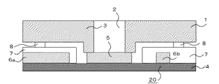
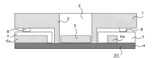
図1〜図4に基づいて本発明の実施の形態1を説明する。図1に示す断面図は、はんだ印刷用に使われるマスク1がプリント配線板20に対向配置されている状態を表している。この状態で、ペースト状のクリームはんだをスキージを用いてプリント配線板20に印刷する。マスク1は、SUS304やSUS301といったステンレス等の金属薄板から形成されることが多い。マスク1には、筒状のポスト3を有する開口2が穿設されている。ポスト3は、プリント配線板20に向かって凸に設けられている。開口2の内寸法は、マスク1の上面(下端)からポスト3の先端まで、マスクの厚さ方向に一定である。
A first embodiment of the present invention will be described with reference to FIGS. The cross-sectional view shown in FIG. 1 shows a state in which a
ベース基材4はプリント配線板20のベースとなる基板材料である。パッド5にはクリームはんだが転写される。パッド5と配線パターン6a、6bは、リソグラフィで得られ、高さが揃っている。ソルダーレジスト7はベース基材4の特定領域に施される耐熱性被覆材料で、クリームはんだを塗布する際にこの特定領域にはんだが付着しないようにカバーする樹脂である。配線パターン6a、6bはソルダーレジスト7で被覆されているが、電子部品が接合されるパッド5にはソルダーレジスト7は塗布されていない。ベース基材4には、パッド5、配線パターン6、ソルダーレジスト7、シンボルプリント8が配置されていて、プリント配線板20を構成している。
The base substrate 4 is a substrate material that becomes the base of the printed
シンボルプリント8は、ソルダーレジスト7の上部に、特定の文字をプリント配線板用語で印刷したものである。文字は、部品No、極性、ピンNo等を表していて、プリント配線板20の最上面に印刷される。クリームはんだ印刷用のマスク1はシンボルプリント8に接触する。シンボルプリント8が無いプリント配線板20の場合、マスク1はソルダーレジスト7に接するため、ポスト3の高さはソルダーレジスト7の厚さのみにする必要がある。
The
開口2はマスク1をプリント配線板20に設定した際、パッド5の上に来るように穿設されている。ポスト3の高さは、ソルダーレジスト7とシンボルプリント8の厚さを加算した厚さ以上とし、少なくともパッド5とポスト3との隙間ははんだの粒子径(例えば20μm)以下にする。これにより、スキージングにより開口2を充満したクリームはんだは、マスク1に配置した開口2から僅かにしか吐出しない場合でも確実にパッド5に接触する。マスク1をプリント配線板20から離すことで、パッド5上にクリームはんだのパターンを転写できる。一般的にソルダーレジスト7とシンボルプリント8の厚さを加算した厚さは5〜50μmであり、ポスト3の高さをこれと同等以上の高さにする。
The
マスク1とパッド5の間に隙間があると、この隙間から、マスク1に配置した開口2の周囲にクリームはんだが滲み出す。パッド5の周辺に印刷されたクリームはんだは部分的に凝集し、はんだボールを発生させる。加熱によりはんだが溶融した状態になるとこのはんだボールは流動し、電子部品の端子間でショート欠陥が発生する。本実施の形態にかかわるマスクでは、マスク1とパッド5に隙間が生じないので、電子部品の端子間でショート欠陥を防止できる。
If there is a gap between the
開口2の内寸法は、マスク1の上面(下端)からポスト3の先端まで一定であることが好ましい。開口2の内寸法が、マスクの厚さ方向に一定であると、開口2の内側に、突出しているところ或いはへこんでいるところがない。特許文献1のように遮断壁をマスクの開口部から少し内側に後退したところに形成すると、遮断壁ははんだの吹き溜まりとして作用する。クリームはんだを開口に充填する際、この吹き溜まりにはんだが取られるので、はんだとパッドの接触が不十分になる。吹き溜まりに残ったはんだは、拭き取りにくいので清掃が不完全になるが、本願に係わるマスクは、清掃が容易である。
The inner dimension of the
また、開口2に半田が途中で吹き溜まる所がなくなると、マスク1をプリント配線板20から剥がしたとき、開口2の内側に充填したクリームはんだやポスト3で囲まれたクリームはんだが、途中で、或いはポスト3のエッジで、切れることがなくなり、電子部品との未接合欠陥が減少する。
Further, when there is no place where the solder is sprayed in the middle of the
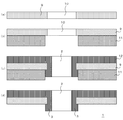
図2は、実施の形態1〜3に係わる平面図で、ポスト3と、パッド5と、配線パターン6の関係を一枚の図にまとめて提示している。プリント配線板20の上にマスク1が間隔をあけて配置されている。マスク1には3種類の形態のポスト3が形成されている。上段が実施の形態1に、中段が実施の形態2に、下段が実施の形態3にそれぞれ対応する。プリント配線板20には図1と同様に配線パターン6a、6bが設けられている。下段では配線パターン6aとパッド5の間は引き出し線14で接続されている。開口2は、マスク1に複数個設けられている。開口2の全周を囲む筒状のポスト3は、周囲のポストおよび開口とは互いに無関係に独立している。独立しているため、隣接する開口部間に設けられる遮断壁とは異なり、隣接する開口と無関係にポスト3の高さ、厚み、形状を設計できる。
FIG. 2 is a plan view according to the first to third embodiments and presents the relationship among the
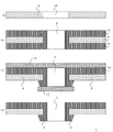
実施の形態1に係わるポスト3を配置したマスク1は図3(a)〜図3(d)に示す方法で得られる。図3(a)はステンレス合金等の金属板9に例えばCO2レーザやエッチング、或いはパンチングやドリル加工で孔10を形成した状態を表している。その後、図3(b)のようにめっきレジスト11をフォトリソグラフィで所望の位置に形成し、図3(c)のように金属めっき12(例えばNi合金)をポスト3が所望の高さになる厚さまでめっきする。その後めっきレジスト11を剥離除去することで図3(d)に示すポスト3を配置したマスク1が得られる。この方法で得られるマスク1は、開口2の内寸法が先端から下端までマスク1の厚さ方向に一定である。金属板9は金属層15で片面が被覆され、開口2の内側も金属層15で被覆され、ポスト3と繋がっている。
The
図4(a)〜図4(d)はマスク1の別の制作方法を示している。図4(a)ではステンレス合金等の金属板9にCO2レーザ等で孔10を形成している。図4(b)のように金属めっき(例えばNi合金)12をポスト3が所望の高さになる厚さまで全面にめっきする。その後図4(c)のようにエッチングレジスト13をフォトリソグラフィで所望の位置に形成する。エッチング液(例えば塩化第二鉄)でウェットエッチング後、レジスト13を剥離除去すれば、図4(d)に示すポスト3を配置したマスク1が得られる。
4A to 4D show another production method of the
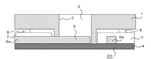
実施の形態2.
図5は実施の形態2に係わるマスクを示す断面図である。マスク1に設けられているポスト3の内寸法は、パッド5の外寸法よりも大きく取られている。開口2の形状は、ここでは方形であるが、パッド5が円柱状であれば円形にすることができる。実施の形態2に関わるパッドとポストの関係を表すのが、図2の中段に示された平面図である。ポスト3はパッド5の上面に接触するのではなく、パッド5の周辺のベース基材4にまで達している。この場合も実施の形態1と同様の効果が得られる。
FIG. 5 is a sectional view showing a mask according to the second embodiment. The inner dimension of the
実施の形態3.
図6は実施の形態3に係わるマスクを示す図である。配線パターン6aとパッド5の間は引き出し線14で接続されている。実施の形態3に関わるパッドとポストの関係を表すのが、図2の下段に示された平面図である。引き出し配線14の上部にポスト3の先端が接触するように高さを一部変更して切り欠き15を設けることで実施形態1と同様の効果を奏する。
FIG. 6 shows a mask according to the third embodiment. The
1 マスク、2 開口、3 ポスト、4 ベース基材、5 パッド、6 パターン、7 ソルダーレジスト、8 シンボルプリント、9 金属板、10 加工孔、11 めっきレジスト、12 金属めっき、13 エッチングレジスト、14 引き出し配線、15 切り欠き、20 プリント配線板 1 mask, 2 openings, 3 posts, 4 base substrate, 5 pads, 6 patterns, 7 solder resist, 8 symbol print, 9 metal plate, 10 processed holes, 11 plating resist, 12 metal plating, 13 etching resist, 14 drawer Wiring, 15 notches, 20 printed wiring board
Claims (8)
Priority Applications (1)
| Application Number | Priority Date | Filing Date | Title |
|---|---|---|---|
| JP2010044133A JP2011181663A (en) | 2010-03-01 | 2010-03-01 | Mask for solder printing |
Applications Claiming Priority (1)
| Application Number | Priority Date | Filing Date | Title |
|---|---|---|---|
| JP2010044133A JP2011181663A (en) | 2010-03-01 | 2010-03-01 | Mask for solder printing |
Publications (1)
| Publication Number | Publication Date |
|---|---|
| JP2011181663A true JP2011181663A (en) | 2011-09-15 |
Family
ID=44692885
Family Applications (1)
| Application Number | Title | Priority Date | Filing Date |
|---|---|---|---|
| JP2010044133A Pending JP2011181663A (en) | 2010-03-01 | 2010-03-01 | Mask for solder printing |
Country Status (1)
| Country | Link |
|---|---|
| JP (1) | JP2011181663A (en) |
Cited By (1)
| Publication number | Priority date | Publication date | Assignee | Title |
|---|---|---|---|---|
| US10332865B2 (en) | 2016-08-22 | 2019-06-25 | Samsung Electronics Co., Ltd. | Method of fabricating light emitting diode module |
-
2010
- 2010-03-01 JP JP2010044133A patent/JP2011181663A/en active Pending
Cited By (1)
| Publication number | Priority date | Publication date | Assignee | Title |
|---|---|---|---|---|
| US10332865B2 (en) | 2016-08-22 | 2019-06-25 | Samsung Electronics Co., Ltd. | Method of fabricating light emitting diode module |
Similar Documents
| Publication | Publication Date | Title |
|---|---|---|
| TW200906245A (en) | Printed circuit board and manufacturing method thereof | |
| US7586754B2 (en) | Printed wiring board and process for manufacturing the same | |
| JP2007214534A (en) | Manufacturing method of circuit board having conductive structure | |
| TW201426932A (en) | Circuit board and manufacturing method thereof | |
| JP2020109836A (en) | Circuit board structure and manufacturing method of the same | |
| TWI545709B (en) | Semiconductor package manufacturing method | |
| CN101287331B (en) | Conductive structure of electric connection pad of circuit board | |
| JP2011181663A (en) | Mask for solder printing | |
| JP2011040720A (en) | Printed circuit board and manufacturing method thereof | |
| JP4512772B2 (en) | Method for manufacturing conductive ball mounting mask | |
| KR200465585Y1 (en) | Mask for various type | |
| JP5500373B2 (en) | Manufacturing method of terminal connection | |
| JP5308689B2 (en) | Local solder amount increasing type metal mask and manufacturing method thereof | |
| US8105644B2 (en) | Manufacturing method of printed circuit board | |
| JP2006287060A (en) | Circuit board and chip component soldering structure | |
| JP2009010257A (en) | Solder printing method, mask for the same, and solder printed circuit board | |
| US20090080170A1 (en) | Electronic carrier board | |
| CN101370356B (en) | Circuit board and its manufacturing method | |
| JP2008041848A (en) | Soldering structure | |
| JP2005243723A (en) | Mask for settling conductive ball | |
| JP2024036232A (en) | wiring board | |
| JP4872736B2 (en) | How to connect electronic devices | |
| JP2008066344A (en) | Multilayer board, and printing method of metal bonding material | |
| JP2005219381A (en) | Screen printing mask and method of manufacturing printed circuit board using the same | |
| JP6763607B2 (en) | Lead frame and its manufacturing method |