JP2011134581A - Plasma display panel - Google Patents
Plasma display panel Download PDFInfo
- Publication number
- JP2011134581A JP2011134581A JP2009292885A JP2009292885A JP2011134581A JP 2011134581 A JP2011134581 A JP 2011134581A JP 2009292885 A JP2009292885 A JP 2009292885A JP 2009292885 A JP2009292885 A JP 2009292885A JP 2011134581 A JP2011134581 A JP 2011134581A
- Authority
- JP
- Japan
- Prior art keywords
- transparent
- electrode
- bus
- electrodes
- plate
- Prior art date
- Legal status (The legal status is an assumption and is not a legal conclusion. Google has not performed a legal analysis and makes no representation as to the accuracy of the status listed.)
- Pending
Links
Images


Abstract
Description
本発明は、プラズマディスプレイパネル(以下、PDPとよぶ。)に関し、特に交流駆動面放電型PDPにおける電極構造の改良に関する。 The present invention relates to a plasma display panel (hereinafter referred to as “PDP”), and more particularly to improvement of an electrode structure in an AC driven surface discharge type PDP.
PDPは、Ne、XeやAr等のガスをプラズマ放電させ、発生した紫外線により蛍光体を励起発光させ可視光に変換して、画像表示を行う表示装置である。このPDPには、交流(以下、ACとよぶ。)駆動型と直流(以下、DCとよぶ。)駆動型がある。AC駆動型は、輝度、発光効率および寿命の各性能面でDC駆動型より優れており、PDPでは主流の駆動方式となっている。 The PDP is a display device that displays an image by causing plasma discharge of a gas such as Ne, Xe, or Ar, and exciting and emitting phosphors with generated ultraviolet rays to convert them into visible light. This PDP includes an alternating current (hereinafter referred to as AC) drive type and a direct current (hereinafter referred to as DC) drive type. The AC drive type is superior to the DC drive type in terms of performance in terms of luminance, light emission efficiency, and lifetime, and the PDP is the main driving method.
AC駆動型として代表的な交流面放電型PDPの構成の一例を、図7及び図8に示す。図7は、前面板1と背面板8を分離した状態でPDPの一部を示した斜視図である。図8は、図7の前面板1と背面板8が合体された状態を示し、図7における走査電極3および維持電極4を横切る方向に沿った断面図である。
An example of the configuration of an AC surface discharge type PDP representative as an AC drive type is shown in FIGS. FIG. 7 is a perspective view showing a part of the PDP in a state where the
前面板1は、透明で絶縁性を有する前面側基板2の表面上に、面放電を行う走査電極3および維持電極4からなる表示電極対5が平行に配列された構成を有する。走査電極3および維持電極4はそれぞれ、前面側基板2の表面上に形成された透明電極3a、4aと、その上に形成されたバス電極3b、4bとにより構成される。バス電極3b、4bは、例えば、銀(Ag)とその結着材であるガラスフリット材料からなる。そして表示電極対5を覆うように前面側誘電体層6が形成され、その上に保護膜7が形成されている。
The
一方、背面板8は、透明で絶縁性を有する背面側基板9の表面上に、画像データを書き込むためのアドレス電極10が、前面側基板2の表示電極対5に対して直交する方向に配列され、その上が背面側誘電体層11で覆われた構成を有する。背面側誘電体層11上には、隔壁12が形成されている。隔壁12は、アドレス電極10に平行な方向に伸びて形成された縦隔壁12aと、それと直交する方向に形成された横隔壁12bとで形成された井桁形状をしている。縦隔壁12aと横隔壁12bとで囲まれた領域により、各画素が規定される。各画素の領域における、隔壁12の側面と背面側誘電体層11の表面とには、アドレス電極10に対応して赤色(R)蛍光体層13r、緑色(G)蛍光体層13g、青色(B)蛍光体層13b(総称して「蛍光体層13」とも記す)が塗布形成されている。
On the other hand, on the
前面板1と背面板8とは、表示電極対5とアドレス電極10とがマトリックスを形成するように対向している。前面板1と背面板8の間で縦隔壁12aと横隔壁12bとで囲まれた空間が、各画素の放電空間14となる。各放電空間14に対応して、表示電極対5とアドレス電極10とが立体交差することにより、放電セル15が形成される。前面板1の表示電極対5の間には、横隔壁12bの上部に対向するようにブラックストライプ16が形成されている。
The
前面板1と背面板8との外周部はガラスフリットなどの封着材によって封着され(図示せず)、放電空間14に、ネオン(Ne)とキセノン(Xe)の混合ガスからなる放電ガスが封入されている。放電ガスは、例えば、Xeの割合が10%のものが用いられ、約450Torr(約60kPa)の圧力で封入される。
The outer peripheral portions of the
上記構成のPDPにおいて、ガス放電により紫外線を発生させ、発生した紫外線でR、G、Bの各色の蛍光体層13を励起して発光させることによりカラー表示を行う。すなわち、バス電極3b、4bを介して維持電極4と走査電極3間に数十〜数百kHzの交流電圧を印加して放電させると、励起されたXe原子が基底状態に戻る際に発生する紫外線により蛍光体層13を励起することができる。この励起により蛍光体層13は、塗布された材料に応じた色光を発生する。アドレス電極10により発光させる画素および色の選択を行えば、所定の画素部で必要な色を発光させることができ、カラー画像を表示することが可能となる。
In the PDP having the above configuration, ultraviolet light is generated by gas discharge, and the
このような構成のAC駆動型のPDPでは、表示電極対5上に形成された前面側誘電体層6が特有の電流制限機能を発揮するので、DC駆動型のPDPに比べて長寿命である。前面側誘電体層6は、表示電極対5とブラックマトリクス16の形成後で、しかも、これらを確実に覆うように形成することが必要とされる。そのため、一般的には低融点ガラスの層を、印刷・焼成方式により形成している。また、保護膜7はプラズマ放電により前面側誘電体層6がスパッタリングされないようにするために設けるもので、耐スパッタリング性に優れた材料であることが要求される。このために、酸化マグネシウム(MgO)が多く用いられている。
In the AC drive type PDP having such a configuration, the front-side
以上のようなPDPにおいて、表示電極対5と放電空間との間に介在させる前面側誘電体層6を、図9に示すように、マイクロシート等の誘電体用薄板17に置き換えた構成が知られている。
In the PDP as described above, a configuration is known in which the front-side
この場合、誘電体用薄板17には、その放電空間14側に保護膜7が形成される。また、前面側である他方の面に、透明電極3a、4a及びバス電極3b、4bからなる表示電極対5が設けられる。更に、表示電極対5を被覆して、透明な絶縁膜18が形成される。そして、誘電体用薄板17の放電空間14側が、低融点ガラス等のシール材で背面側基板9に封着される。一方、誘電体用薄板17上には一定の間隙19を設けて、透明保護基板としての前面側基板2が接合される。
In this case, the
このように、前面側誘電体層6に代えて誘電体用薄板17を使用することにより、誘電体層を形成するための従来の煩雑な製造プロセスを簡略化することができる。また、誘電体用薄板17を低融点ガラス等のシール材で背面側基板9に封着することにより、前面側基板2は、製造工程中に高温に曝されることがなくなる。
Thus, by using the dielectric
ここで、マイクロシートとは、例えば二酸化シリコン(SiO2)と三酸化硼素(B2O3)を主成分とする硼珪酸ガラスなどの薄い誘電体シートである。厚みは、30μm程度、最大でも50μm程度である。このようなマイクロシートは、例えば液晶表示装置のシートとして広く利用されており、耐熱性が高く線膨張係数が小さい。 Here, the microsheet is a thin dielectric sheet such as borosilicate glass mainly composed of silicon dioxide (SiO 2 ) and boron trioxide (B 2 O 3 ). The thickness is about 30 μm and at most about 50 μm. Such a microsheet is widely used, for example, as a sheet for a liquid crystal display device, and has high heat resistance and a low linear expansion coefficient.
このように、誘電体用薄板にバス電極と透明電極が形成された構成は、例えば特許文献1に開示されている。また、例えば特許文献2には、誘電体用薄板を用いたPDPであって、前面基板にバス電極と透明電極が形成された構成が開示されている。
Thus, the structure in which the bus electrode and the transparent electrode are formed on the dielectric thin plate is disclosed in, for example,
一般的なPDP表示装置では、PDPのバス電極と駆動回路の接続工程において、フレキシブル基板を用いてPDPの前面板のバス電極と駆動回路とが接続される。その際のフレキシブル基板とバス電極との接続は、両者間に異方性導電フィルムを介在させて、フレキシブル基板の電極部とバス電極を位置合わせして、加熱しながら加圧する方法により行われる。その後、接続部は、水分による影響を抑制するための樹脂でモールドされる。 In a general PDP display device, the bus electrode on the front plate of the PDP and the drive circuit are connected using a flexible substrate in the connection process of the bus electrode of the PDP and the drive circuit. In this case, the flexible substrate and the bus electrode are connected by a method in which an anisotropic conductive film is interposed therebetween, the electrode portion of the flexible substrate and the bus electrode are aligned, and pressure is applied while heating. Thereafter, the connecting portion is molded with a resin for suppressing the influence of moisture.
特許文献1に記載されたような、誘電体用薄板にバス電極と透明電極が形成されたPDPの構成の場合、誘電体用薄板上のバス電極とフレキシブル基板の電極部を接続するときの加熱、加圧に際して、誘電体薄板が割れ易い。この割れの問題を解決するためには、誘電体用薄板のバス電極を背面基板に延長すればよいが、バス電極を背面基板に延長する工程は難しく、また新たな工程が追加されることになる。従って、根本的に、PDPのバス電極とフレキシブル基板の接続工程を排除することは困難である。
In the case of a PDP configuration in which a bus electrode and a transparent electrode are formed on a dielectric thin plate as described in
また、特許文献2に記載されたような、誘電体用薄板を用い、前面基板にバス電極と透明電極が設けられた構成の場合でも、前面基板のバス電極とフレキシブル基板の接続工程が必要であった。
In addition, even in the case of using a dielectric thin plate as described in
以上のとおり、従来のPDPの構成では、フレキシブル基板とパネルのバス電極の接続工程が必要であるため、製造工程が長くなる。 As described above, the conventional PDP configuration requires a process of connecting the flexible substrate and the bus electrode of the panel, and therefore the manufacturing process becomes long.
また、誘電体用薄板を用いたPDPであって、前面基板に透明電極とバス電極が形成された構成の場合、光の取り出し効率を上げるためにバス電極を細く厚くすることが困難であった。 Further, in the case of a PDP using a dielectric thin plate, in which a transparent electrode and a bus electrode are formed on the front substrate, it is difficult to make the bus electrode thin and thick in order to increase the light extraction efficiency. .
すなわち、光の取り出し効率を上げるには、バス電極による発光の遮蔽をできるだけ減らすために、バス電極を細くする必要がある。ところが、バス電極は各セルに放電電流を供給する機能を求められているにもかかわらず、バス電極が細くなるとバス電極の抵抗値が上昇するので、電圧降下が生じて各セルに所定の電圧を印加することが困難になる。そのため、バス電極を細くしてもバス電極の抵抗値を同等以下にすべく、バス電極を厚くする必要がある。 That is, in order to increase the light extraction efficiency, it is necessary to make the bus electrode thinner in order to reduce the light shielding by the bus electrode as much as possible. However, the bus electrode is required to have a function of supplying a discharge current to each cell, but if the bus electrode becomes thin, the resistance value of the bus electrode increases, so that a voltage drop occurs and a predetermined voltage is applied to each cell. Is difficult to apply. Therefore, even if the bus electrode is thinned, it is necessary to increase the thickness of the bus electrode so that the resistance value of the bus electrode is equal to or less.
ここで、誘電体用薄板を用いたPDPに適応した構造を考えると、前面基板の上に透明電極を形成し、さらにその上にバス電極を形成することになる。従って、光の取り出し効率を上げるためにバス電極を厚くすると、放電の制御に重要な透明電極が誘電体から離間した状態になる。その結果、透明電極で形成される電界による放電空間への作用が弱くなるので、バス電極の形状、位置が放電を支配するようになる。 Here, considering a structure suitable for a PDP using a dielectric thin plate, a transparent electrode is formed on the front substrate, and a bus electrode is further formed thereon. Therefore, when the bus electrode is made thicker in order to increase the light extraction efficiency, the transparent electrode important for the discharge control is separated from the dielectric. As a result, the action of the electric field formed by the transparent electrode on the discharge space is weakened, so that the shape and position of the bus electrode dominate the discharge.
ところが、フォトリソグラフィとエッチングによりバス電極のパターンを形成するとき、バス電極が厚いと、バラツキが生れやすい。特に、バス電極間の距離で決まる放電ギャップは放電開始電圧を決める重要なパラメータであり、バス電極間の距離にバラツキが生じると、放電開始電圧がバラツキ、画像にムラが生じる。また、バス電極が形成される前面基板と背面基板の組み立て精度により、バス電極の位置が変わると、隔壁とバス電極の位置関係のずれによって、放電開始電圧のバラツキが大きくなり、画像にムラが生じる。 However, when the bus electrode pattern is formed by photolithography and etching, variation is likely to occur if the bus electrode is thick. In particular, the discharge gap determined by the distance between the bus electrodes is an important parameter for determining the discharge start voltage, and when the distance between the bus electrodes varies, the discharge start voltage varies and the image becomes uneven. Also, if the position of the bus electrode changes due to the assembly accuracy of the front substrate and the rear substrate on which the bus electrode is formed, the variation in the discharge start voltage increases due to the positional relationship between the barrier rib and the bus electrode, and the image is uneven. Arise.
以上の問題を考慮して、本発明は、バス電極とフレキシブル基板の接続工程を不要とし、製造時間の短縮、製造エネルギーの減少を可能とする環境に良好な構成を有するプラズマディスプレイパネルを提供することを目的とする。 In view of the above problems, the present invention provides a plasma display panel having a favorable configuration in an environment that eliminates the step of connecting a bus electrode and a flexible substrate, reduces manufacturing time, and reduces manufacturing energy. For the purpose.
また、光の取り出し効率を上げて、低消費電力化を可能とした構成においても、透明電極で形成される電界による放電空間への作用を十分に大きくできるプラズマディスプレイパネルを提供することを目的とする。 It is another object of the present invention to provide a plasma display panel that can sufficiently increase the effect of an electric field formed by a transparent electrode on a discharge space even in a configuration capable of increasing light extraction efficiency and reducing power consumption. To do.
上記課題を解決するために、本発明のプラズマディスプレイパネルは、前面側基板上に走査電極および維持電極からなる複数の表示電極対を構成するためのバス電極が設けられた前面板と、背面側基板上に前記表示電極対と立体交差する複数のアドレス電極が設けられ、前記アドレス電極と前記表示電極対の交差部に各々放電セルを区画する隔壁が設けられ、前記隔壁間に蛍光体層が設けられた背面板と、前記前面板と前記背面板の間に配置された誘電体用薄板と、前記複数の表示電極対を構成するように前記バス電極に対応させて、前記前面側基板上の前記バス電極の下層として配置された透明電極、または前記前面板と前記誘電体用薄板との間に配置された透明電極とを備え、前記前面側基板は表示領域の外部に延在する接続配線部を有し、前記バス電極は前記接続配線部に延在して接続配線を形成しており、前記接続配線の端部は駆動回路と接続可能な端子部として機能することを特徴とする。 In order to solve the above-described problems, a plasma display panel according to the present invention includes a front plate provided with bus electrodes for forming a plurality of display electrode pairs including scan electrodes and sustain electrodes on a front substrate, and a rear side. A plurality of address electrodes that are three-dimensionally crossed with the display electrode pair are provided on a substrate, and a partition wall that partitions discharge cells is provided at an intersection of the address electrode and the display electrode pair, and a phosphor layer is provided between the partition walls. The back plate provided, the dielectric thin plate disposed between the front plate and the back plate, and the bus electrodes so as to form the plurality of display electrode pairs, A connection wiring portion including a transparent electrode disposed as a lower layer of a bus electrode, or a transparent electrode disposed between the front plate and the dielectric thin plate, wherein the front substrate extends outside a display region. Have , The bus electrode forms a connection wiring extending to the connection wiring part, the ends of the connection line may be functioning as a terminal portion connectable to a drive circuit.
上記構成によれば、前面側基板が表示領域の外部に延在する接続配線部を有し、バス電極に繋がっている接続配線により駆動回路と接続可能であるため、前面側基板は駆動回路用ケーブルの機能を兼用し、フレキシブル基板とバス電極との接続工程を不要とすることができる。 According to the above configuration, the front substrate has the connection wiring portion extending outside the display area, and can be connected to the drive circuit by the connection wiring connected to the bus electrode. The function of the cable is also used, and the connection process between the flexible substrate and the bus electrode can be eliminated.
本発明のプラズマディスプレイパネルは上記構成を基本として、以下のような態様をとることができる。 The plasma display panel of the present invention can take the following modes based on the above-described configuration.
すなわち、前記透明電極は、前記誘電体用薄板の前記前面板に対向する面上に設けられた構成とすることが好ましい。この構成によれば、放電空間に対して透明電極がバス電極よりも近接し、透明電極で形成される電界による放電空間への作用を十分に大きく確保できる。しかも、透明電極を、バス電極と同様にフォトリソグラフィとエッチングにより形成したとしても、透明電極は薄いので、形状バラツキが小さくなるため、放電開始電圧のバラツキが抑えられ、画像にムラがなくなる。 That is, it is preferable that the transparent electrode is provided on a surface of the dielectric thin plate facing the front plate. According to this configuration, the transparent electrode is closer to the discharge space than the bus electrode, and a sufficiently large action on the discharge space by the electric field formed by the transparent electrode can be ensured. Moreover, even if the transparent electrode is formed by photolithography and etching in the same manner as the bus electrode, since the transparent electrode is thin, the variation in shape is reduced, so that the variation in discharge start voltage is suppressed and the image is not uneven.
この構成において、前記透明電極と前記バス電極との間に絶縁性接着層が設けられている構成とすることができる。 In this configuration, an insulating adhesive layer may be provided between the transparent electrode and the bus electrode.
あるいは、前記透明電極と前記バス電極との間に導電性接着層が設けられている構成としてもよい。 Alternatively, a conductive adhesive layer may be provided between the transparent electrode and the bus electrode.
これらの構成において、前記前面側基板上の前記バス電極及び前記透明電極の間に透明絶縁層が形成され、前記誘電体用薄板の周縁部が接着剤により前記前面板に接合されている構成とすることができる。 In these configurations, a transparent insulating layer is formed between the bus electrode and the transparent electrode on the front substrate, and a peripheral portion of the dielectric thin plate is bonded to the front plate by an adhesive. can do.
あるいは、前記前面側基板上の前記バス電極及び前記透明電極の間に絶縁性透明接着層が形成され、前記誘電体用薄板の全面が、前記絶縁性透明接着層により前記前面板に接合されている構成とすることができる。 Alternatively, an insulating transparent adhesive layer is formed between the bus electrode and the transparent electrode on the front substrate, and the entire surface of the dielectric thin plate is bonded to the front plate by the insulating transparent adhesive layer. It can be set as a structure.
また、前記バス電極は、前記前面側基板上に形成された絶縁性透明樹脂層中に先端部を露出させて埋め込まれ、前記透明電極は、前記バス電極を含む前記絶縁性透明樹脂層の面上に形成されている構成とすることができる。この構成の場合も、上述の、透明電極が誘電体用薄板の前面板に対向する面上に設けられた構成と同様、放電開始電圧のバラツキが抑えられ、画像にムラがなくなる効果を得ることができる。 Further, the bus electrode is embedded in an insulating transparent resin layer formed on the front substrate with the tip portion exposed, and the transparent electrode is a surface of the insulating transparent resin layer including the bus electrode. It can be set as the structure currently formed on the top. In the case of this configuration as well as the above-described configuration in which the transparent electrode is provided on the surface facing the front plate of the dielectric thin plate, the variation in the discharge starting voltage is suppressed, and the effect of eliminating the unevenness in the image is obtained. Can do.
この構成において、前記絶縁性透明樹脂層上の前記透明電極の間に透明絶縁層が形成され、前記誘電体用薄板の周縁部が接着剤により前記前面板に接合されている構成とすることができる。 In this configuration, a transparent insulating layer is formed between the transparent electrodes on the insulating transparent resin layer, and a peripheral portion of the dielectric thin plate is bonded to the front plate by an adhesive. it can.
あるいは、前記絶縁性透明樹脂層上の前記透明電極の間に絶縁性透明接着層が形成され、前記誘電体用薄板の全面が、前記絶縁性透明接着層により前記前面板に接合されている構成とすることができる。 Alternatively, an insulating transparent adhesive layer is formed between the transparent electrodes on the insulating transparent resin layer, and the entire surface of the dielectric thin plate is joined to the front plate by the insulating transparent adhesive layer. It can be.
以下、本発明の実施の形態について図面を参照しながら説明する。なお、本発明の実施の形態のPDPの基本的な構成要素は、図9に示した従来例のPDPと同様である。従って、図9に示した要素と同一の要素については、同一の参照符号を付して説明し、重複した説明を簡略にする。 Hereinafter, embodiments of the present invention will be described with reference to the drawings. The basic components of the PDP according to the embodiment of the present invention are the same as those of the conventional PDP shown in FIG. Therefore, the same elements as those shown in FIG. 9 are described with the same reference numerals, and the overlapping description is simplified.
(実施の形態1)
実施の形態1におけるPDPの構成について、図1A及び図1Bを参照して説明する。図1A及び図1Bはそれぞれ、実施の形態1におけるPDPの2つの構成例の一部を示す断面図である。
(Embodiment 1)
The configuration of the PDP in
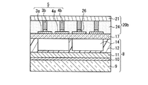
本実施の形態のPDPの第1構成例について、図1Aを参照して説明する。まず、背面板8は、図7〜図9に示した従来例と同様の構造である。更に、前面板20aと背面板8の間に、誘電体用薄板17が配置されている。すなわち、背面板8の上部は誘電体用薄板17により封止され、背面板8と誘電体用薄板17により「背面側構造体」が形成されている。
A first configuration example of the PDP according to the present embodiment will be described with reference to FIG. 1A. First, the
前面板20aは、基本構成として、透明で絶縁性を有する前面側基板21と、その内面側に設けられたバス電極3b、4bとを含む。バス電極3b、4bの各々の間には、透明絶縁層22が形成されている。透明絶縁層22は、バス電極3b、4bの表面上で起こる沿面放電抑制のために設けられる。前面板20aと誘電体用薄板17は、周縁部で接着剤23により接合されている。
The
透明電極とバス電極3b、4bは、従来例と同様、走査電極3および維持電極4からなる複数の表示電極対を構成する。背面板8では、背面側基板9上に表示電極対と立体交差する複数のアドレス電極10が設けられている。更に、アドレス電極10と表示電極対の交差部に各々放電セルを形成するための放電空間14を区画する隔壁12が設けられ、隔壁12間に蛍光体層(図示せず。図7〜図9参照)が設けられている。
The transparent electrodes and the
本実施の形態の特徴として、前面側基板21は、図2に示すような平面構造を有する。すなわち、前面側基板21は、表示領域21aの外部に延在する接続配線部21bを有する。バス電極3b、4bは、接続配線部21bに延在して接続配線3c、4cを形成している。接続配線3c、4cの端部は、接続配線部21bの周縁端部である端子部21cに配置されて、駆動回路(図示せず)と接続される。接続配線3c、4cは、表示領域21a及び端子部21c以外では透明基材で覆われていることが望ましい。
As a feature of the present embodiment, the
この構成によれば、前面側基板21が表示領域21aの外部に延在する接続配線部21bを有し、バス電極3b、4bに繋がっている接続配線3c、4cにより駆動回路と接続可能であるため、前面側基板21は駆動回路用ケーブルの機能を兼用し、フレキシブル基板とバス電極との接続工程を省略することが可能となる。従って、製造時間の短縮、簡略化に寄与し、製造エネルギーの低減を図ることができる。
According to this configuration, the
なお、図1Aには図示が省略されているが、実際には、複数の表示電極対を構成するようにバス電極3b、4bに対応させて透明電極が設けられている。透明電極は、前面側基板21上のバス電極3b、4bの下層として、または誘電体用薄板17の前面板20aに対向する面上に配置される。
In addition, although illustration is abbreviate | omitted in FIG. 1A, the transparent electrode is actually provided corresponding to the
図1Bに示す本実施の形態のPDPの第2構成例の前面板20bでは、透明絶縁層22に代えて絶縁性透明接着層24が用いられる。それにより、周縁部で接着剤23により接合するのではなく、全面で絶縁性透明接着層24により接合される。
In the
以上のように、実施の形態1のPDPの基本構成は、前面板(前面側基板+バス電極++接続配線部+絶縁層)と、(背面板+誘電体用薄板)が組合わされたものである。 As described above, the basic configuration of the PDP according to the first embodiment is a combination of a front plate (front substrate + bus electrode + + connection wiring part + insulating layer) and (back plate + dielectric thin plate). is there.
上記構成のPDPを作製するためには、従来周知の製造工程を一部変更して適用することができる。先ず、背面板8を作製するために、背面側基板9にアドレス電極10、隔壁12、及び蛍光体層を、それぞれスクリーン印刷法により形成する。また、誘電体用薄板17の上にMgO保護膜(図示せず)を形成する。MgO保護膜は、誘電体用薄板17の保護膜を付けるべき範囲に電子線蒸着法により形成する。さらに、前面板20aを作製するために、前面側基板21の内部側の面にバス電極3b、4bを形成する。この工程については後述する。
In order to fabricate the PDP having the above-described configuration, it is possible to apply a modification of a part of a conventionally known manufacturing process. First, in order to manufacture the
その後、MgO保護膜が形成された誘電体用薄板17を、背面板8の隔壁12と密着させて低融点ガラス(図示せず)により封着し、放電ガスを満たしてチップオフする。その後、背面板8上に封着された誘電体用薄板17と前面板20aとを、例えば、常温下で接着剤により貼り合わせてパネル化する。
Thereafter, the dielectric
前面板20aと誘電体用薄板17(+背面板8)の接着は、例えば、以下のようにして行うことができる。前面板20aを構成する前面側基板21は透明基板で形成されているため、高温プロセスに耐えることができない。従って、前面板20aと誘電体用薄板17の接着は低温プロセスで行わなければならない。
The
すなわち、図1Aに示した第1構成例のように、前面板20aと誘電体用薄板17の周縁部のみを接続する場合は、絶縁性接着剤23を用いることができる(透明である必要はない)。また、図1Bに示した第2構成例のように、前面板20aと誘電体用薄板17を面全体で接続する場合は、エポキシ接着剤、アクリル接着剤等の絶縁性透明接着層24を用いる。
That is, as in the first configuration example shown in FIG. 1A, the insulating
次に、前面板20aを作製するための工程について、以下に説明する。まず、前面基板21としては、例えば、ポリエチレンテレフタレート(PET)、ポリカーボネート(PC)、ポリエチレンナフタレート(PEN)、ポリイミド(PI)等を用いることができる。特に、誘電率の低い材料が望ましい。無効電力を削減できるからである。
Next, the process for producing the
バス電極3b、4bを細く、厚く形成するために、アディティブ工法(特に、セミアディティブ工法)を用いることができる。あるいは、サブトラクティブ工法を用いてもよい。アディティブ工法とは、絶縁樹脂上に、必要な部分だけに金属メッキを施して配線パターンを作成する方法である。サブトラクティブ工法とは、絶縁樹脂の全面に金属膜を形成した後、不要な金属の部分を除去し、配線パターンを作成する方法である。
In order to form the
セミアディティブ工法によるバス電極3b、4bの形成工程では、まず、無電解メッキにより前面基板21の全面に、シールド層として、金属メッキを施す(例えば銅メッキ)。その上にレジストを貼り付けて、配線パターン以外の部分にレジストが残るように、露光・現像する。次に、電解メッキにより、レジスト以外の部分に金属メッキを施し、レジストを剥離した後、シールド層をエッチングにより除去する。セミアディティブ工法によれば、高アスペクト比のバス電極3b、4bの形成が可能である。バス電極の厚さは10μm以上とする。他の電極材料としては、銀、金、Ni等を用いることができる。
In the process of forming the
透明絶縁層22は、以下のような方法により形成することができる。第1例は、バス電極に、例えば有機珪素系のオーバーコート剤を塗布・乾燥・熱処理することで、絶縁被膜を形成する方法である。
The transparent insulating
第2例は、前面板20aと誘電体用薄板17の間の空間を絶縁性透明液体で満たす方法である。絶縁性透明液体としては、例えば、シリコンオイル、鉱油、シリコンゴム、エポキシ樹脂、紫外線硬化樹脂、低分子の液状樹脂等を用いることができる。絶縁性透明液体の充填には、例えば、以下のような方法を用いることができる。
The second example is a method of filling the space between the
すなわち、前面板20a上の一カ所にバス電極3b、4bを横切る様に一定量のシリコーンオイル等の液状の絶縁性透明液体を、ディスペンサ法(注射針のような細い管から液体を塗布する方法)により塗布する。そして、前面板20aと誘電体用薄板17とを貼り合わせる。例えばシリコーンオイルは、ガラス面に対して濡れやすい性質をもつので、前面板20aと誘電体用薄板17との間に充填されると、毛細管現象により、バス電極3b、4b間の空間にも濡れ広がる。このようにして、必要な量のシリコーンオイルを前面板20aの中央部に最適な面積だけ塗布することにより、前面板20aの端部からあふれることなく、前面板20aの全面に均一に充填される。シリコーンオイルを一定量塗布してから、前面板20aと誘電体用薄板17とを重ね、一定の重量の重りをおいて、全面に加重をかけることにより、シリコーンオイルは全面に均一に充填される。
That is, a certain amount of liquid insulating transparent liquid such as silicone oil is applied to one place on the
透明絶縁層22を形成する第3例の方法は、前面板20aと誘電体用薄板17の間の空間を絶縁性気体で満たす方法である。絶縁性気体としては、例えば空気、窒素、六フッ化イオウ等の無色透明な気体を用いることができる。
The third example method for forming the transparent insulating
誘電体用薄板17としては、例えば、二酸化シリコン(SiO2)と三酸化硼素(B2O3)を主成分とする硼珪酸ガラス、BaOとAl2O3を多く含んだ硼珪酸系無アルカリガラスなどの薄い誘電体シートを用いることができる。厚みは、10〜40μm程度で最大でも50μm程度である。あるいは、厚い誘電体シートを使用して、封着し、その後、研磨して薄く(10〜40um)して誘電体用薄板17としてもよい。
Examples of the dielectric
上記構成において、前面板20aに他の機能も持たせることができる。例えば、外部の衝撃から保護するための保護基板、カラーフィルタ、ブラックストライプ、反射防止フィルム、電磁波シールド等である。
In the above configuration, the
(実施の形態2)
実施の形態2におけるPDPについて、図3A〜図3Bを参照して説明する。図3A〜図3Bは、本実施の形態における2つの構成例のPDPの一部を示す断面図である。
(Embodiment 2)
The PDP in
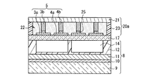
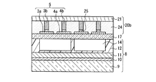
本実施の形態のPDPの基本構成について、図3Aを参照して説明する。このPDPの構成は、概ね図1Aに示した実施の形態1におけるPDPと同様である。従って、図1Aに示した要素と同様の要素については同一の参照符号を付して、重複する説明は省略する。
A basic configuration of the PDP according to the present embodiment will be described with reference to FIG. 3A. The configuration of this PDP is generally the same as that of the PDP in
前面板20aは、実質的に実施の形態1の場合と同様の構成であり、前面側基板21と、その内面側に設けられたバス電極3b、4bと、バス電極3b、4bの間に形成された透明絶縁層22からなる。
The
背面板8と誘電体用薄板17が組合された背面側構造体の構成は、実施の形態1と同様である。但し、誘電体用薄板17の前面板20aと対向する面に、透明電極3a、4aが設けられている。前面板20aと誘電体用薄板17は、周縁部で接着剤23により接合されている。
The configuration of the back side structure in which the
図3Bに示す第2構成例の前面板20bでは、図1Bに示した構成例と同様、透明絶縁層22に代えて絶縁性透明接着層24が用いられる。それにより、周縁部で接着剤23により接合するのではなく、全面で絶縁性透明接着層24により接合される。
In the
以上のように、実施の形態2のPDPの基本構成は、前面板(前面側基板+バス電極++接続配線部+絶縁層)と、(背面板+(誘電体用薄板+透明電極))が組合わされたものである。本実施の形態の構成は、次のような課題を解決するために用いられる。 As described above, the basic configuration of the PDP of the second embodiment is that the front plate (front substrate + bus electrode + + connection wiring part + insulating layer) and (back plate + (thin dielectric plate + transparent electrode)). It is a combination. The configuration of the present embodiment is used to solve the following problems.
(1)輝度を確保するにはある程度の電極面積が必要となる。しかし、バス電極3b、4bの面積が広がると光の取り出し効率が悪くなり、輝度が低下する。これに対して本実施の形態では、透明電極3a、4aを誘電体用薄板17の前面板20aと対向する面に設けることによって、光を遮光するバス電極3b、4bの面積は小さくして、透明電極3a、4aで電極面積を確保する。透明電極3a、4aは光の遮光はほとんどないので、光の取り出し効率があがる。
(1) A certain amount of electrode area is required to ensure luminance. However, when the area of the
(2)フォトリソグラフィーとエッチングによりバス電極3b、4bのパターンを形成する際には、バス電極3b、4bが厚いため、電極形状及び位置のバラツキが発生し易い。特に、バス電極間の距離で決まる放電ギャップは放電開始電圧を決める重要なパラメータであり、バス電極間の距離にバラツキが生じると、放電開始電圧がバラツキ、画像にムラが生じる。透明電極3a、4aを誘電体用薄板17の前面板20aと対向する面に設けることによって、この問題も解決できる。すなわち、バス電極3b、4bと同じエッチングにより透明電極3a、4aを形成したとしても、透明電極3a、4aは薄いので、形状バラツキが小さく、電極間の距離のバラツキが小さいので、放電開始電圧のバラツキが抑えられ、画像にムラがなくなる。
(2) When the patterns of the
(3)バス電極3b、4bが形成される前面基板21と、背面板8の組み立て精度により、バス電極3b、4bの位置が変動する。隔壁12とバス電極3b、4bの位置関係のずれによって、放電開始電圧のバラツキが大きくなり、画像にムラが生じる。透明電極3a、4aを誘電体用薄板17の前面板20aと対向する面に設けた場合、透明電極3a、4aを封着後に形成すれば、前面基板21と背面板8の組立て精度による放電開始電圧のバラツキが抑えられ、画像にムラがなくなる。
(3) The position of the
上記構成のPDPを作製するためには、概ね実施の形態1のPDPと同様のプロセスを用いることができる。実施の形態1のプロセス異なるのは、透明電極3a、4aを形成するプロセスである。透明電極3a、4aは、誘電体用薄板17を用意するプロセスにおいて、保護膜形成前に保護膜面の反対側にITO膜を真空蒸着して、フォトリソグラフィー法によりエッチングでパターン形成する。
In order to manufacture the PDP having the above structure, a process similar to that of the PDP in
または、背面板8と誘電体用薄板17を封着、排気、ガス封入、チップオフした後、インクジェットによる直描により誘電体用薄板17に透明電極パターンを形成し、低温加熱した後、前面板20bと張り合わせる。封着後に透明電極3a、4aを形成するので、封着による位置ずれを、透明電極3a、4aの形成時に補正できる。
Alternatively, the
絶縁層は、バス電極3b、4b、透明電極3a、4aともに設ける。絶縁層の形成は、実施の形態1と同様の方法で行なうことができる。また、絶縁性透明接着層24を用いて、前面板20bと(誘電体用薄板17+背面板8)を面全体で接合する場合は、バス電極3b、4b、透明電極3a、4aに絶縁層を設けなくてもよい。
The insulating layer is provided for both the
透明電極3a、4aとしては、例えば、インジウム錫酸化物(ITO)、酸化錫(SnO2)、酸化亜鉛(ZnO)等を用いることができる。
As the
また、透明電極以外に、ブラックストライプ、及びカラーフィルタを、透明電極と同じようにチップオフ後、直描で形成することもできる。また、全面あるいは一部に紫外線防止層(350nm以下を通さない)を形成することもできる。紫外線防止層の役割は、有機物系の劣化を防ぐこと、例えば、前面基板21の透明基板、カラーフィルタ、ブラックストライプ等の劣化を防ぐことである。
In addition to the transparent electrode, the black stripe and the color filter can be formed by direct drawing after chip-off in the same manner as the transparent electrode. Further, an ultraviolet ray preventing layer (not passing through 350 nm or less) can be formed on the entire surface or a part thereof. The role of the ultraviolet ray preventing layer is to prevent deterioration of organic materials, for example, deterioration of the transparent substrate, the color filter, the black stripe, etc. of the
透明電極3a、4aをチップオフ後に形成する場合は、その後のプロセスは低温プロセスのみとなる。従って、ブラックストライプ、カラーフィルタ、紫外線防止層の材質として、高温プロセスには耐えられない、低温プロセスのみ使用できる特性の良い材料(例:有機物)を使うことができる。
When the
(実施の形態3)
実施の形態3におけるPDPについて、図4A〜図4Bを参照して説明する。図4A〜図4Bは、本実施の形態における2つの構成例のPDPの一部を示す断面図である。
(Embodiment 3)
A PDP according to
本実施の形態のPDPの基本構成について、図4Aを参照して説明する。このPDPの構成は、概ね図3Aに示した実施の形態2におけるPDPと同様である。従って、図3Aに示した要素と同様の要素については同一の参照符号を付して、重複する説明は省略する。 A basic configuration of the PDP according to the present embodiment will be described with reference to FIG. 4A. The configuration of this PDP is substantially the same as the PDP in the second embodiment shown in FIG. 3A. Therefore, the same elements as those shown in FIG. 3A are denoted by the same reference numerals, and redundant description is omitted.
前面板20a、及び背面板8と誘電体用薄板17が組合された背面側構造体の構成、及び誘電体用薄板17に設けられた透明電極3a、4aは、実施の形態2と同様である。但し、透明電極3a、4aとバス電極3b、4bの間に、絶縁性接着層25が設けられている。前面板20aと誘電体用薄板17は、周縁部で接着剤23により接合されている。
The configuration of the
一方、図4Bに示す第2構成例の前面板20bでは、図1Bに示した構成例と同様、透明絶縁層22に代えて絶縁性透明接着層24が用いられる。それにより、周縁部で接着剤23により接合するのではなく、全面で絶縁性透明接着層24により接合される。
On the other hand, in the
以上のように、実施の形態3のPDPの基本構成は、前面板(前面側基板+バス電極++接続配線部+絶縁層)と、絶縁性接着層と、(背面板+(誘電体用薄板+透明電極))が組合わされたものである。本実施の形態の構成では、透明電極3a、4aとバス電極3b、4bの間に絶縁性接着層25を設け、容量結合することで透明電極3a、4aに電圧が印加される。
As described above, the basic configuration of the PDP according to the third embodiment includes the front plate (front substrate + bus electrode + + connection wiring part + insulating layer), the insulating adhesive layer, and (back plate + (dielectric thin plate). + Transparent electrode)). In the configuration of the present embodiment, an insulating
すなわち、実施の形態2の構成では、接触接合及び容量結合の両方が同一パネル内に存在するため、透明電極3a、4aに印加される電圧が不均一になり易い。そのため、放電開始電圧が異なり、画像にムラが生じる場合がある。
That is, in the configuration of the second embodiment, since both the contact junction and the capacitive coupling are present in the same panel, the voltage applied to the
これに対して、バス電極3b、4bまたは透明電極3a、4aに絶縁性接着層25を塗布してから接着し、容量結合のみに制限することによって、透明電極3a、4aに印加される電圧を均一にすることができ、画像のムラを解消することができる。
On the other hand, by applying the insulating
上記構成のPDPを作製するためには、概ね実施の形態1のPDPと同様のプロセスを用いることができる。但し、本実施の形態では、透明電極3a、4aまたはバス電極3b、4bに、印刷またはインクジェットによる直描により絶縁性接着層25を塗布してから、前面板20aまたは20bと、(誘電体用薄板17+背面板8)とを接合する。
In order to manufacture the PDP having the above structure, a process similar to that of the PDP in
透明絶縁層22は、バス電極3b、4b及び透明電極3a、4aともに設ける。透明絶縁層22の形成には実施の形態1と同じ方法を用いることができる。
The transparent insulating
バス電極3b、4bと透明電極3a、4aの接続とは別に、前面板と(誘電体用薄板+背面板)を面全体で接続する場合は、絶縁性透明接着層を用いる。この場合、図4Bに示したように、絶縁層の代わりに絶縁性透明接着層24のみで絶縁層の代用をしてもよい。
In addition to the connection between the
また、前面板と(誘電体用薄板+背面板)とを全面で接着する絶縁性透明接着層24と、透明電極3a、4aまたはバス電極3b、4bに塗布する絶縁性接着層25が同じでもよい。
Further, even if the insulating transparent
(実施の形態4)
実施の形態4におけるPDPについて、図5A〜図5Bを参照して説明する。図5A〜図5Bは、本実施の形態における2つの構成例のPDPの一部を示す断面図である。
(Embodiment 4)
The PDP in Embodiment 4 will be described with reference to FIGS. 5A to 5B. FIG. 5A to FIG. 5B are cross-sectional views showing a part of PDPs of two configuration examples in the present embodiment.
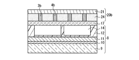
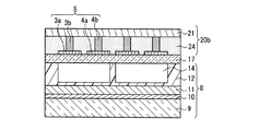
本実施の形態のPDPの基本構成について、図5Aを参照して説明する。このPDPの構成は、概ね図4Aに示した実施の形態3におけるPDPと同様である。但し、透明電極3a、4aとバス電極3b、4bの間に、絶縁性接着層25に代えて導電性接着層26が設けられている。前面板20aと誘電体用薄板17は、周縁部で接着剤23により接合されている。
A basic configuration of the PDP according to the present embodiment will be described with reference to FIG. 5A. The configuration of this PDP is almost the same as that of the PDP in the third embodiment shown in FIG. 4A. However, a conductive
図5Bに示す第2構成例の前面板20bでは、図1Bに示した構成例と同様、透明絶縁層22に代えて絶縁性透明接着層24が用いられる。それにより、周縁部で接着剤23により接合するのではなく、全面で絶縁性透明接着層24により接合される。
In the
以上のように、実施の形態4のPDPの基本構成は、前面板(前面側基板+バス電極++接続配線部+絶縁層)と、導電性接着層と、(背面板+(誘電体用薄板+透明電極))が組合わされたものである。本実施の形態の構成では、透明電極3a、4aとバス電極3b、4bの間に導電性接着層26を設けて、電気伝導により透明電極3a、4aに電圧が印加される。
As described above, the basic configuration of the PDP according to the fourth embodiment includes the front plate (front substrate + bus electrode + + connection wiring portion + insulating layer), the conductive adhesive layer, and (back plate + (dielectric thin plate). + Transparent electrode)). In the configuration of the present embodiment, a conductive
本実施の形態の構成は、実施の形態3と同様の課題を解決するものである。すなわち、バス電極3b、4bまたは透明電極3a、4aに導電性接着層26を塗布してから接着し、容量結合を排除することによって、透明電極3a、4aに印加される電圧を均一にすることができ、画像のムラを解消することができる。
The configuration of the present embodiment solves the same problem as that of the third embodiment. That is, by applying the conductive
上記構成のPDPを作製するためには、概ね実施の形態3のPDPと同様のプロセスを用いることができる。すなわち、実施の形態3の絶縁性接着層25と同様にして導電性接着層26を設けることができる。また、絶縁層の配置、絶縁層の形成方法、あるいは絶縁性透明接着層を用いる構成等も、実施の形態3と同様である。
In order to manufacture the PDP having the above configuration, a process similar to that of the PDP in
導電性接着層26としては、バス電極3b、4bの下部のみに形成する場合、透明である必要はないので、例えば、銀ペースト(銀フィラー+エポキシ樹脂)等を使用することができる。また、バス電極3b、4bの下部からはみ出す可能性が高い場合は、できるだけ透明である必要がある。例えば、上記と同じ銀ペーストでも、銀フィラーの量をできるだけ減らしたものを使用する、または銀フィラーの代わりにITOフィラーを混ぜたITOペーストを使用する。
When the conductive
(実施の形態5)
実施の形態5におけるPDPについて、図6A〜図6Bを参照して説明する。図6A〜図6Bは、本実施の形態における2つの構成例のPDPの一部を示す断面図である。
(Embodiment 5)
A PDP according to
本実施の形態のPDPの基本構成について、図6Aを参照して説明する。このPDPの構成は、基本的な形態としては、図3Aに示した実施の形態2におけるPDPと同様であるが、透明電極3a、4aの配置が図3Aの構成とは相違し、前面板20c上に設けられている。
A basic configuration of the PDP according to the present embodiment will be described with reference to FIG. 6A. The basic configuration of this PDP is the same as that of the PDP in the second embodiment shown in FIG. 3A, but the arrangement of the
すなわち、前面基板21上の絶縁性透明樹脂層27中にバス電極3b、4bが埋め込まれ、バス電極3b、4bの端面を含む絶縁性透明樹脂層27上に透明電極3a、4aが形成されている。透明電極3a、4aの各々の間には透明絶縁層22が設けられ、前面板20cと誘電体用薄板17は、周縁部で接着剤23により接合されている。
That is, the
図6Bに示す第2構成例の前面板20dでは、図1Bに示した構成例と同様、透明絶縁層22に代えて絶縁性透明接着層24が用いられる。それにより、周縁部で接着剤23により接合するのではなく、全面で絶縁性透明接着層24により接合される。
In the
以上のように、実施の形態5のPDPの基本構成は、前面板(前面側基板+バス電極+透明電極+接続配線部+絶縁層)と、(背面板+誘電体用薄板)が組合わされたものである。本実施の形態の構成は、透明電極3a、4aをバス電極3b、4bよりも放電空間14の側に配置するために、実施の形態2とは異なる形態を用いたものであり、その目的は実施の形態2の場合と同様、放電開始電圧のバラツキを抑え、画像のムラを解消することである。
As described above, the basic configuration of the PDP of the fifth embodiment is a combination of the front plate (front substrate + bus electrode + transparent electrode + connection wiring part + insulating layer) and (back plate + dielectric thin plate). It is a thing. The configuration of the present embodiment uses a form different from that of the second embodiment in order to dispose the
上記構成のPDPを作製するためには、前面板20cあるいは20dの作製を次のように行なう。すなわち、セミアディティブ法で、バス電極パターンまで形成した前面基板21上のバス電極3b、4b間に絶縁性透明樹脂を流し込み、平坦化する。その後、インクジェット等で透明電極3a、4aを印刷して、低温で焼成して透明電極3a、4aを完成する。前面板20c、20dと背面板8の接続方法は、上記実施の形態と同様に行なうことができる。
In order to manufacture the PDP having the above configuration, the
本発明のPDPは、前面側基板が駆動回路用ケーブルの機能を兼用し、フレキシブル基板とバス電極との接続工程を省略することが可能となるので、壁掛けテレビや大型モニターとして有用である。 The PDP of the present invention is useful as a wall-mounted television or a large monitor because the front substrate also serves as a drive circuit cable and the connection process between the flexible substrate and the bus electrode can be omitted.
1、20a、20b、20c、20d 前面板
2、21 前面側基板
3 走査電極
3a、4a 透明電極
3b、4b バス電極
3c、4c 接続配線
4 維持電極
5 表示電極対
6 前面側誘電体層
7 保護膜
8 背面板
9 背面側基板
10 アドレス電極
11 背面側誘電体層
12 隔壁
12a 縦隔壁
12b 横隔壁
13 蛍光体層
13r 赤色(R)蛍光体層
13g 緑色(G)蛍光体層
13b 青色(B)蛍光体層
14 放電空間
15 放電セル
16 ブラックストライプ
17 誘電体用薄板
18 絶縁被覆膜
19 間隙
21a 表示領域
21b 接続配線部
21c 端子部
22 透明絶縁層
23 接着剤
24 絶縁性透明接着層
25 絶縁性接着層
26 導電性接着層
27 絶縁性透明樹脂層
1, 20a, 20b, 20c,
Claims (9)
背面側基板上に前記表示電極対と立体交差する複数のアドレス電極が設けられ、前記アドレス電極と前記表示電極対の交差部に各々放電セルを区画する隔壁が設けられ、前記隔壁間に蛍光体層が設けられた背面板と、
前記前面板と前記背面板の間に配置された誘電体用薄板と、
前記複数の表示電極対を構成するように前記バス電極に対応させて、前記前面側基板上の前記バス電極の下層として配置された透明電極、または前記前面板と前記誘電体用薄板との間に配置された透明電極とを備え、
前記前面側基板は表示領域の外部に延在する接続配線部を有し、前記バス電極は前記接続配線部に延在して接続配線を形成しており、前記接続配線の端部は駆動回路と接続可能な端子部として機能することを特徴とするプラズマディスプレイパネル。 A front plate provided with bus electrodes for constituting a plurality of display electrode pairs consisting of scan electrodes and sustain electrodes on a front substrate;
A plurality of address electrodes that are three-dimensionally crossed with the display electrode pair are provided on a back side substrate, and a partition that partitions discharge cells is provided at the intersection of the address electrode and the display electrode pair, and a phosphor is provided between the partitions. A back plate provided with a layer;
A dielectric thin plate disposed between the front plate and the back plate;
A transparent electrode disposed as a lower layer of the bus electrode on the front substrate, or between the front plate and the dielectric thin plate, corresponding to the bus electrode so as to constitute the plurality of display electrode pairs And a transparent electrode disposed on the
The front-side substrate has a connection wiring portion extending outside the display area, the bus electrode extends to the connection wiring portion to form a connection wiring, and an end portion of the connection wiring is a drive circuit A plasma display panel that functions as a terminal portion that can be connected to a plasma display panel.
Priority Applications (1)
| Application Number | Priority Date | Filing Date | Title |
|---|---|---|---|
| JP2009292885A JP2011134581A (en) | 2009-12-24 | 2009-12-24 | Plasma display panel |
Applications Claiming Priority (1)
| Application Number | Priority Date | Filing Date | Title |
|---|---|---|---|
| JP2009292885A JP2011134581A (en) | 2009-12-24 | 2009-12-24 | Plasma display panel |
Publications (2)
| Publication Number | Publication Date |
|---|---|
| JP2011134581A true JP2011134581A (en) | 2011-07-07 |
| JP2011134581A5 JP2011134581A5 (en) | 2013-01-31 |
Family
ID=44347094
Family Applications (1)
| Application Number | Title | Priority Date | Filing Date |
|---|---|---|---|
| JP2009292885A Pending JP2011134581A (en) | 2009-12-24 | 2009-12-24 | Plasma display panel |
Country Status (1)
| Country | Link |
|---|---|
| JP (1) | JP2011134581A (en) |
Cited By (3)
| Publication number | Priority date | Publication date | Assignee | Title |
|---|---|---|---|---|
| KR101624101B1 (en) | 2015-02-17 | 2016-05-25 | (주)레온 | Flexible led display device based on transparent pcb |
| WO2016186468A1 (en) * | 2015-05-20 | 2016-11-24 | (주)레온 | Transparent pcb-based flexible led display device |
| KR101764409B1 (en) * | 2017-01-13 | 2017-08-02 | 주식회사 라임디스플레이 | A Flexible LED Display Device with Transparent PCB And Manufacturing Method Thereof |
Citations (5)
| Publication number | Priority date | Publication date | Assignee | Title |
|---|---|---|---|---|
| JPH05250992A (en) * | 1992-03-04 | 1993-09-28 | Nec Corp | Plasma display panel |
| JPH0816131A (en) * | 1994-06-28 | 1996-01-19 | Sharp Corp | Image display device |
| JPH10340676A (en) * | 1997-04-10 | 1998-12-22 | Fujitsu Ltd | Plasma display panel and its manufacture |
| JP2002202752A (en) * | 2000-12-28 | 2002-07-19 | Gendai Plasma Kk | Ac-type pdp device having small number of wires between signal processing board and panel |
| JP2007234282A (en) * | 2006-02-28 | 2007-09-13 | Matsushita Electric Ind Co Ltd | Plasma display panel and method for fabrication thereof |
-
2009
- 2009-12-24 JP JP2009292885A patent/JP2011134581A/en active Pending
Patent Citations (5)
| Publication number | Priority date | Publication date | Assignee | Title |
|---|---|---|---|---|
| JPH05250992A (en) * | 1992-03-04 | 1993-09-28 | Nec Corp | Plasma display panel |
| JPH0816131A (en) * | 1994-06-28 | 1996-01-19 | Sharp Corp | Image display device |
| JPH10340676A (en) * | 1997-04-10 | 1998-12-22 | Fujitsu Ltd | Plasma display panel and its manufacture |
| JP2002202752A (en) * | 2000-12-28 | 2002-07-19 | Gendai Plasma Kk | Ac-type pdp device having small number of wires between signal processing board and panel |
| JP2007234282A (en) * | 2006-02-28 | 2007-09-13 | Matsushita Electric Ind Co Ltd | Plasma display panel and method for fabrication thereof |
Cited By (3)
| Publication number | Priority date | Publication date | Assignee | Title |
|---|---|---|---|---|
| KR101624101B1 (en) | 2015-02-17 | 2016-05-25 | (주)레온 | Flexible led display device based on transparent pcb |
| WO2016186468A1 (en) * | 2015-05-20 | 2016-11-24 | (주)레온 | Transparent pcb-based flexible led display device |
| KR101764409B1 (en) * | 2017-01-13 | 2017-08-02 | 주식회사 라임디스플레이 | A Flexible LED Display Device with Transparent PCB And Manufacturing Method Thereof |
Similar Documents
| Publication | Publication Date | Title |
|---|---|---|
| US8634040B2 (en) | Multi display device | |
| JP2011134581A (en) | Plasma display panel | |
| KR100858810B1 (en) | Plasma display panel and method of manufacturing the same | |
| KR100383056B1 (en) | Plasma display panel and method for manufacturing the same | |
| JP2003338246A (en) | Plasma display device and its manufacturing method | |
| JP2006120618A (en) | Panel assembly, assembly of plasma display device using this, and manufacturing method of plasma display device assembly | |
| JP2003007218A (en) | Plasma display panel | |
| KR100863911B1 (en) | Plasma display panel | |
| US20070228918A1 (en) | Plasma display module | |
| JPWO2006112419A1 (en) | Plasma display panel | |
| KR100962436B1 (en) | Display Panel | |
| US20080157670A1 (en) | Plasma display panel and method of manufacturing the same | |
| KR100701943B1 (en) | Plasma display panel and method of fabricating the same | |
| JP4333086B2 (en) | Plasma display device | |
| JP2004356039A (en) | Plasma display panel | |
| KR100615193B1 (en) | Plasma display panel | |
| JP2011044355A (en) | Plasma display panel | |
| KR100416082B1 (en) | Plasma display panel | |
| JP2009211062A (en) | Display panel | |
| KR100708703B1 (en) | Plasma display apparatus | |
| KR101070920B1 (en) | Method for forming electrode of plasma display panel | |
| KR20070107272A (en) | Plasma display panel device | |
| US20110221338A1 (en) | Front plate for plasma display panel and method for manufacturing the same, as well as plasma display panel | |
| KR100879471B1 (en) | Plasma display panel and the aligning method thereof | |
| KR100844838B1 (en) | Plasma Display Panel and Method of Fabricating a pair of Sustain Electrodes Thereof |
Legal Events
| Date | Code | Title | Description |
|---|---|---|---|
| A711 | Notification of change in applicant |
Free format text: JAPANESE INTERMEDIATE CODE: A711 Effective date: 20120110 |
|
| A521 | Written amendment |
Free format text: JAPANESE INTERMEDIATE CODE: A821 Effective date: 20120110 |
|
| A521 | Written amendment |
Free format text: JAPANESE INTERMEDIATE CODE: A523 Effective date: 20121210 |
|
| A621 | Written request for application examination |
Free format text: JAPANESE INTERMEDIATE CODE: A621 Effective date: 20121210 |
|
| A977 | Report on retrieval |
Free format text: JAPANESE INTERMEDIATE CODE: A971007 Effective date: 20130422 |
|
| A131 | Notification of reasons for refusal |
Free format text: JAPANESE INTERMEDIATE CODE: A131 Effective date: 20130611 |
|
| A521 | Written amendment |
Free format text: JAPANESE INTERMEDIATE CODE: A523 Effective date: 20130704 |
|
| A131 | Notification of reasons for refusal |
Free format text: JAPANESE INTERMEDIATE CODE: A131 Effective date: 20131212 |
|
| A02 | Decision of refusal |
Free format text: JAPANESE INTERMEDIATE CODE: A02 Effective date: 20140513 |