JP2011108252A - Memory card, data processor, and control method and setting method for memory card - Google Patents
Memory card, data processor, and control method and setting method for memory card Download PDFInfo
- Publication number
- JP2011108252A JP2011108252A JP2010285813A JP2010285813A JP2011108252A JP 2011108252 A JP2011108252 A JP 2011108252A JP 2010285813 A JP2010285813 A JP 2010285813A JP 2010285813 A JP2010285813 A JP 2010285813A JP 2011108252 A JP2011108252 A JP 2011108252A
- Authority
- JP
- Japan
- Prior art keywords
- memory card
- error correction
- data
- read
- memory
- Prior art date
- Legal status (The legal status is an assumption and is not a legal conclusion. Google has not performed a legal analysis and makes no representation as to the accuracy of the status listed.)
- Granted
Links
- 238000000034 method Methods 0.000 title claims abstract description 81
- 230000006870 function Effects 0.000 claims abstract description 70
- 230000004044 response Effects 0.000 claims description 6
- 230000008569 process Effects 0.000 abstract description 62
- 230000005540 biological transmission Effects 0.000 abstract 1
- 238000007726 management method Methods 0.000 description 38
- 230000005856 abnormality Effects 0.000 description 5
- 238000013500 data storage Methods 0.000 description 4
- 101100328887 Caenorhabditis elegans col-34 gene Proteins 0.000 description 3
- 230000002159 abnormal effect Effects 0.000 description 3
- 238000010586 diagram Methods 0.000 description 2
- RRLHMJHRFMHVNM-BQVXCWBNSA-N [(2s,3r,6r)-6-[5-[5-hydroxy-3-(4-hydroxyphenyl)-4-oxochromen-7-yl]oxypentoxy]-2-methyl-3,6-dihydro-2h-pyran-3-yl] acetate Chemical compound C1=C[C@@H](OC(C)=O)[C@H](C)O[C@H]1OCCCCCOC1=CC(O)=C2C(=O)C(C=3C=CC(O)=CC=3)=COC2=C1 RRLHMJHRFMHVNM-BQVXCWBNSA-N 0.000 description 1
- 230000008901 benefit Effects 0.000 description 1
- 230000008859 change Effects 0.000 description 1
- 230000002950 deficient Effects 0.000 description 1
- 238000012986 modification Methods 0.000 description 1
- 230000004048 modification Effects 0.000 description 1
Images


Classifications
-
- G—PHYSICS
- G06—COMPUTING; CALCULATING OR COUNTING
- G06F—ELECTRIC DIGITAL DATA PROCESSING
- G06F13/00—Interconnection of, or transfer of information or other signals between, memories, input/output devices or central processing units
- G06F13/38—Information transfer, e.g. on bus
- G06F13/382—Information transfer, e.g. on bus using universal interface adapter
- G06F13/385—Information transfer, e.g. on bus using universal interface adapter for adaptation of a particular data processing system to different peripheral devices
-
- G—PHYSICS
- G06—COMPUTING; CALCULATING OR COUNTING
- G06F—ELECTRIC DIGITAL DATA PROCESSING
- G06F11/00—Error detection; Error correction; Monitoring
- G06F11/07—Responding to the occurrence of a fault, e.g. fault tolerance
- G06F11/0703—Error or fault processing not based on redundancy, i.e. by taking additional measures to deal with the error or fault not making use of redundancy in operation, in hardware, or in data representation
- G06F11/0706—Error or fault processing not based on redundancy, i.e. by taking additional measures to deal with the error or fault not making use of redundancy in operation, in hardware, or in data representation the processing taking place on a specific hardware platform or in a specific software environment
- G06F11/073—Error or fault processing not based on redundancy, i.e. by taking additional measures to deal with the error or fault not making use of redundancy in operation, in hardware, or in data representation the processing taking place on a specific hardware platform or in a specific software environment in a memory management context, e.g. virtual memory or cache management
-
- G—PHYSICS
- G06—COMPUTING; CALCULATING OR COUNTING
- G06F—ELECTRIC DIGITAL DATA PROCESSING
- G06F11/00—Error detection; Error correction; Monitoring
- G06F11/07—Responding to the occurrence of a fault, e.g. fault tolerance
- G06F11/08—Error detection or correction by redundancy in data representation, e.g. by using checking codes
- G06F11/10—Adding special bits or symbols to the coded information, e.g. parity check, casting out 9's or 11's
- G06F11/1008—Adding special bits or symbols to the coded information, e.g. parity check, casting out 9's or 11's in individual solid state devices
- G06F11/1048—Adding special bits or symbols to the coded information, e.g. parity check, casting out 9's or 11's in individual solid state devices using arrangements adapted for a specific error detection or correction feature
- G06F11/1052—Bypassing or disabling error detection or correction
-
- G—PHYSICS
- G06—COMPUTING; CALCULATING OR COUNTING
- G06F—ELECTRIC DIGITAL DATA PROCESSING
- G06F11/00—Error detection; Error correction; Monitoring
- G06F11/07—Responding to the occurrence of a fault, e.g. fault tolerance
- G06F11/0703—Error or fault processing not based on redundancy, i.e. by taking additional measures to deal with the error or fault not making use of redundancy in operation, in hardware, or in data representation
- G06F11/0793—Remedial or corrective actions
-
- G—PHYSICS
- G11—INFORMATION STORAGE
- G11C—STATIC STORES
- G11C29/00—Checking stores for correct operation ; Subsequent repair; Testing stores during standby or offline operation
- G11C29/04—Detection or location of defective memory elements, e.g. cell constructio details, timing of test signals
- G11C2029/0409—Online test
Abstract
Description
本発明は、書き換え可能な不揮発性メモリを備え、ホストに装着して使用されるメモリカードであって、特に、データ書き込み時のリトライ機能またはデータ読み出し時のエラー訂正機能を有するメモリカード及びそのようなメモリカードにアクセスするデータ処理装置(ホスト)に関する。 The present invention relates to a memory card that includes a rewritable nonvolatile memory and is used by being mounted on a host, and in particular, a memory card having a retry function at the time of data writing or an error correction function at the time of data reading, and the like The present invention relates to a data processing apparatus (host) that accesses a simple memory card.
近年、デジタル情報を保存する記憶装置として、書き換え可能な不揮発性メモリを搭載したメモリカードや機器が普及してきている。特にメモリカードは、小型かつ耐震性に優れるため、今後、益々携帯機器で多用されることが期待されている。 In recent years, memory cards and devices equipped with a rewritable nonvolatile memory have become widespread as storage devices for storing digital information. In particular, since memory cards are small and have excellent earthquake resistance, it is expected that they will be increasingly used in portable devices in the future.
書き換え可能な不揮発性メモリの代表的なものにNAND型フラッシュメモリ(以下、「フラッシュメモリ」と称す。)がある。フラッシュメモリは、ブロック単位でその使用、未使用が管理されており、例えば、未使用のブロックに関して、管理データにおいて“1”が書き込まれ、データの書き込みを行った場合に、管理データを“1”から“0”に書き換える。 A typical rewritable nonvolatile memory is a NAND flash memory (hereinafter referred to as “flash memory”). In the flash memory, use and non-use are managed in units of blocks. For example, “1” is written in the management data for unused blocks, and when the data is written, the management data is set to “1”. Rewrite from “0” to “0”.
また、一般的に、フラッシュメモリは、正常に書き込まれない場合が希に存在する。このため、フラッシュメモリには、正常書き込みであったか、または異常書き込みであったかを示すステータスをリード(読み出し)する機能が備わっており、データの書き込み後、このステータスをリードすることによって、書き込みが正常に行なわれたか否かを判別することが必要である。メモリカードによっては、フラッシュメモリを制御するコントローラが内蔵されており、コントローラがデータ書き込み後にステータスリードを行い、書き込みエラーが発生した場合は、そのブロックが再び書き込みブロックとして選択されないようにするために、コントローラに内蔵された、エラーが発生したブロックに対応する管理データを“1”から“0”に書き換える。 In general, there are rare cases where flash memory is not normally written. For this reason, the flash memory has a function of reading (reading) the status indicating whether it was normal writing or abnormal writing. By writing this status after writing data, the writing can be performed normally. It is necessary to determine whether it has been done. Some memory cards have a built-in controller that controls the flash memory.If the controller performs a status read after writing data and a write error occurs, the block is not selected as a write block again. The management data corresponding to the block in which an error has occurred is rewritten from “1” to “0”.
また、正常にデータが書き込まれなかった場合すなわち書き込み時にエラーが発生した場合、そのデータを再度別のブロックに書き込みを行う処理(以下「リトライ処理」と称す。)も提案されている。なお、書き込み時のエラーは、フラッシュメモリの空き容量がない場合、データを書き込もうとしたフラッシュメモリの領域が不良であるため書き込みが行えない場合、書き込み時のイレース処理の失敗時等に発生する。 In addition, there has been proposed a process (hereinafter referred to as “retry process”) in which data is not written normally, that is, when an error occurs during writing, the data is written again into another block. Note that an error at the time of writing occurs when there is no free space in the flash memory, when writing cannot be performed because the area of the flash memory to which data is written is defective, or when the erase process at the time of writing fails.
また、フラッシュメモリに書き込まれたデータにおいて、他ブロックへのデータ書き込みによって、また、経年変化によって、希にデータ化けが発生する。このため、メモリカードとして所望のデータ信頼性を確保するために、データ読み出し時は、例えば、ブロック単位で、フラッシュメモリの信頼性に応じた誤り訂正符号を生成し、ブロックのデータに付加して、フラッシュメモリに書き込む。また、データ読み出し時には、読み出されたデータに対して誤り訂正処理を行った後、ホストへ転送する。 In addition, in the data written in the flash memory, data corruption occurs rarely due to data writing to other blocks or due to secular change. Therefore, in order to ensure the desired data reliability as a memory card, when reading data, for example, an error correction code corresponding to the reliability of the flash memory is generated and added to the block data in units of blocks. Write to flash memory. At the time of data reading, error correction processing is performed on the read data and then transferred to the host.
以上のように、フラッシュメモリに希に発生する書き込みエラー、読み出しエラーは、殆どの場合、メモリカードに内蔵されたコントローラによってリトライ処理、及び誤り訂正処理を行うことによって回避される。このため、ホスト機器はフラッシュメモリのデータ信頼性を考慮することなくメモリカードを使用することができる。 As described above, write errors and read errors that rarely occur in the flash memory are avoided in most cases by performing retry processing and error correction processing by a controller built in the memory card. Therefore, the host device can use the memory card without considering the data reliability of the flash memory.
以上のような、フラッシュメモリの書き込みエラーに対するリトライ処理に関する技術として特許文献1に記載されたものが知られている。
A technique described in
しかしながら、近年、メモリカードは、民生用途のみならず、業務用途の様々なホスト機器に用いられ始め、ホストによっては、従来のメモリカードの信頼性では、不十分な場合もある。 However, in recent years, memory cards have begun to be used not only for consumer use but also for various host devices for business use, and depending on the host, the reliability of conventional memory cards may be insufficient.
書き込みエラーが発生しやすいフラッシュメモリにおいて、書き込みエラーが発生した場合のリトライ処理により、ホストに対して書き込みエラーとして通知される頻度が低減される。これにより、ホストによっては、書き込みエラーとして通知された場合の特別な処理を考慮することが無く、ホストの処理負担が軽減するという長所がある。しかしながら、リトライ処理はフラッシュメモリの内部で行われるため、フラッシュメモリ上で書き込みエラーが発生しているのか、リトライ処理が行われているのかどうか、ホスト側では全く分からない。リトライ処理によって書き込み時間が非常に長くなり、更に、リトライ処理においても書き込みエラーが発生した場合、リトライ処理の間、書き込み完了の通知を待たされたあげく、書き込みエラーになることもあった。 In a flash memory in which a write error is likely to occur, the frequency of being notified as a write error to the host is reduced by retry processing when a write error occurs. As a result, there is an advantage that the processing load of the host is reduced without considering special processing when notified as a write error depending on the host. However, since the retry process is performed inside the flash memory, the host side does not know at all whether a write error has occurred in the flash memory or the retry process is being performed. When the retry process makes the write time very long, and when a write error occurs in the retry process, a write completion notification may be waited during the retry process, and a write error may occur.
静止画を記録するデジタルスチルカメラの場合は、リアルタイムでの処理が要求されないため、書き込みエラー通知された後でもホストによる対応は可能である。しかし、動画を記録するビデオカメラの場合、リアルタイムでの処理が要求される。メモリカードにおいてリトライ処理が実行されると、書き込み時間が長くなる場合があるため、ビデオカメラ(ホスト)側で書き込み時間を見積もりにくく、ビデオカメラ(ホスト)でのデータ処理が非常に難しくなるという課題がある。このように、メモリカードにおけるリトライ処理は、リアルタイム処理を要求するホストにおいては、有効な機能とならない場合もある。 In the case of a digital still camera that records a still image, real-time processing is not required, and the host can respond even after a write error is notified. However, a video camera that records a moving image requires real-time processing. When retry processing is executed on a memory card, the write time may become long, so it is difficult to estimate the write time on the video camera (host) side, and the data processing on the video camera (host) becomes very difficult There is. As described above, the retry processing in the memory card may not be an effective function in a host that requests real-time processing.
また、従来のメモリカードは、メモリカードとして所望のデータ信頼性となるように、フラッシュメモリの信頼性に応じて、誤り訂正符号を付加している。例えば、高信頼性のフラッシュメモリを内蔵したメモリカードには1ビット訂正回路が、また、低信頼性のフラッシュメモリを内蔵したメモリカードには3ビット訂正回路が搭載される。メモリカードとしては、何れも同等の信頼性を確保している。3ビット訂正回路を搭載したメモリカードは、3ビットまでの誤りは訂正可能であるが、4ビット以上の誤りが発生した場合には訂正不能となり、ホストに対してエラー通知をするが、場合によっては、誤訂正となり、誤ったデータをホストに返すことになる。通常、このようなケースに陥る確率は非常に低くなるように設定されている。しかし、エラーが通知されたり、或いは誤ったデータが正常データとして読み出されたりする以上、例えば、業務用のホスト等のように、非常に高い信頼性を要求するホストの場合、業務用ホスト側の工夫で、メモリカードの誤り訂正能力以上の信頼性を上げることはできないという課題があった。 Further, the conventional memory card is added with an error correction code according to the reliability of the flash memory so as to obtain desired data reliability as the memory card. For example, a 1-bit correction circuit is mounted on a memory card incorporating a high-reliability flash memory, and a 3-bit correction circuit is mounted on a memory card incorporating a low-reliability flash memory. As memory cards, all have the same reliability. A memory card equipped with a 3-bit correction circuit can correct errors up to 3 bits, but if an error of 4 bits or more occurs, it cannot be corrected and an error is notified to the host. Will be erroneously corrected and return incorrect data to the host. Usually, the probability of falling into such a case is set to be very low. However, since an error is notified or erroneous data is read as normal data, for example, in the case of a host that requires extremely high reliability, such as a business host, the business host side However, there is a problem that the reliability beyond the error correction capability of the memory card cannot be improved.
本発明は上記の課題を解決するためになされたものであり、メモリカードにおけるリトライ処理に起因する弊害や、メモリカードの誤り訂正処理に起因する問題を解決するメモリカード及びメモリカードに対する制御方法等を提供する。 The present invention has been made in order to solve the above-mentioned problems. A memory card and a control method for the memory card that solve problems caused by retry processing in the memory card and problems caused by error correction processing of the memory card, etc. I will provide a.
(1)本発明の第1の態様において、データ処理装置からデータの書き込み、読み出しが可能なメモリカードが提供される。メモリカードは、データ処理装置との間でコマンドやデータの送受信を行うホストインタフェースと、データを格納する不揮発性メモリと、メモリカードの動作を制御するコントローラと、所定の管理情報を格納する記憶手段とを備える。管理情報は、不揮発性メモリへの書き込み動作時にエラーが発生したときにリトライ機能を実行するか否かを指定するためのリトライ設定情報を含む。 (1) In the first aspect of the present invention, a memory card capable of writing and reading data from a data processing device is provided. The memory card includes a host interface that transmits and receives commands and data to and from the data processing device, a nonvolatile memory that stores data, a controller that controls the operation of the memory card, and storage means that stores predetermined management information With. The management information includes retry setting information for designating whether to execute the retry function when an error occurs during a write operation to the nonvolatile memory.
コントローラは、データ書き込み動作時に、リトライ設定情報を参照し、リトライ設定情報がリトライ機能の停止を示す場合は、データ書き込み動作時のエラー発生時にリトライ機能を動作させないように、また、リトライ設定情報がリトライ機能の作動を示す場合は、データ書き込み動作時のエラー発生時にリトライ機能を動作させるように、書き込み動作を制御する。 The controller refers to the retry setting information during the data write operation, and if the retry setting information indicates that the retry function is stopped, the retry function is not operated when an error occurs during the data write operation. When the retry function is activated, the write operation is controlled so that the retry function is activated when an error occurs during the data write operation.
上記のメモリカードにおいて、管理情報はさらにメモリカード固有の特性情報を含んでもよい。そのとき、コントローラはデータ処理装置からの要求に応じて特性情報をデータ処理装置に送信してもよい。 In the above memory card, the management information may further include characteristic information unique to the memory card. At that time, the controller may transmit the characteristic information to the data processing device in response to a request from the data processing device.
特性情報には、メモリカードにおいてデータ書き込みに要する最大の所要時間に関する情報や、メモリカードにおいてリトライ処理が発生する頻度に関する情報が含まれてもよい。 The characteristic information may include information on the maximum required time required for data writing in the memory card and information on the frequency of retry processing occurring in the memory card.
(2)本発明の第2の態様において、データの読み出し、書き込みが可能で、かつ、書き込み動作時にエラーが発生したときにリトライ機能を実行するか否かを指定するためのリトライ設定情報及びメモリカード固有の特性情報を管理情報として格納するメモリカードにアクセス可能なデータ処理装置が提供される。 (2) Retry setting information and memory for specifying whether or not to execute a retry function when an error occurs during a write operation in the second aspect of the present invention. Provided is a data processing device that can access a memory card that stores characteristic information unique to the card as management information.
データ処理装置は、メモリカードとの間でコマンドやデータの送受信を行うカードインタフェースと、データ処理装置の動作を制御するコントローラとを備える。
コントローラは、メモリカードがデータ処理装置に装着されたとき又はデータ処理装置の電源投入時に、メモリカードから特性情報を読み出し、読み出した特性情報に基づき、メモリカードにおいてリトライ機能を実行させるか否かの判断を行い、その判断結果にしたがい、リトライ設定情報を設定するためのコマンドをカードインタフェースを介してメモリカードに送信する。
The data processing device includes a card interface that transmits and receives commands and data to and from the memory card, and a controller that controls the operation of the data processing device.
The controller reads the characteristic information from the memory card when the memory card is inserted in the data processing apparatus or when the data processing apparatus is turned on, and determines whether or not to execute the retry function in the memory card based on the read characteristic information. A determination is made, and a command for setting retry setting information is transmitted to the memory card via the card interface according to the determination result.
(3)本発明の第3の態様において、データの読み出し、書き込みが可能で、かつ、書き込み動作時にエラーが発生したときにリトライ機能を実行するか否かを指定するためのリトライ設定情報を管理情報として格納するメモリカードの制御方法が提供される。その制御方法は、データ書き込み動作時に、リトライ設定情報を参照し、リトライ設定情報がリトライ機能の停止を示す場合は、データ書き込み動作時のエラー発生時にリトライ機能を動作させず、リトライ設定情報がリトライ機能の作動を示す場合は、データ書き込み動作時のエラー発生時にリトライ機能を動作させる。 (3) In the third aspect of the present invention, management of retry setting information for designating whether or not to execute a retry function when an error occurs during a write operation is possible. A method for controlling a memory card to be stored as information is provided. The control method refers to the retry setting information during the data write operation. If the retry setting information indicates that the retry function is stopped, the retry function is not operated when an error occurs during the data write operation, and the retry setting information is retried. When the function is activated, the retry function is activated when an error occurs during the data write operation.
(4)本発明の第4の態様において、データの読み出し、書き込みが可能で、かつ、書き込み動作時にエラーが発生したときにリトライ機能を実行するか否かを指定するためのリトライ設定情報及びメモリカード固有の特性情報を管理情報として格納するメモリカードに対する設定方法が提供される。その設定方法は、メモリカードから前記特性情報を読み出し、読み出した特性情報に基づいて、メモリカードにおいてリトライ処理を実行させるか否かの判断を行い、その判断結果にしたがい、リトライ設定情報を設定するためのコマンドをカードインタフェースを介してメモリカードに送信する。 (4) In the fourth aspect of the present invention, retry setting information and memory for designating whether or not to execute a retry function when an error occurs during a write operation and data can be read and written A setting method is provided for a memory card that stores card-specific characteristic information as management information. The setting method reads the characteristic information from the memory card, determines whether or not to execute a retry process in the memory card based on the read characteristic information, and sets the retry setting information according to the determination result. The command is transmitted to the memory card via the card interface.
(5)本発明の第5の態様において、データ処理装置からデータの書き込み、読み出しが可能なメモリカードが提供される。メモリカードは、データ処理装置との間でコマンドやデータの送受信を行うホストインタフェースと、データを格納する不揮発性メモリと、メモリカードの動作を制御するコントローラと、所定の管理情報を格納する記憶手段とを備える。
管理情報は、不揮発性メモリからのデータの読み出し時に誤り訂正機能を実行するか否かを指定するための誤り訂正設定情報を含む。
コントローラは、データ読み出し動作時に、誤り訂正設定情報を参照し、誤り訂正設定情報が誤り訂正機能の停止を示す場合は、読み出したデータに対して誤り訂正を行わないように、また、誤り訂正設定情報が誤り訂正機能の作動を示す場合は、読み出したデータに対して誤り訂正を行うように、読み出し動作を制御する。
(5) In a fifth aspect of the present invention, there is provided a memory card capable of writing and reading data from a data processing device. The memory card includes a host interface that transmits and receives commands and data to and from the data processing device, a nonvolatile memory that stores data, a controller that controls the operation of the memory card, and storage means that stores predetermined management information With.
The management information includes error correction setting information for designating whether or not to execute the error correction function when reading data from the nonvolatile memory.
The controller refers to the error correction setting information during the data reading operation. When the information indicates the operation of the error correction function, the read operation is controlled so that error correction is performed on the read data.
管理情報はさらにメモリカード固有の特性情報を含み、コントローラはデータ処理装置からの要求に応じて特性情報をデータ処理装置に送信してもよい。
特性情報は、不揮発性メモリの誤り率に関する情報を含んでもよい。
The management information may further include characteristic information unique to the memory card, and the controller may transmit the characteristic information to the data processing apparatus in response to a request from the data processing apparatus.
The characteristic information may include information on the error rate of the nonvolatile memory.
(6)本発明の第6の態様において、データの読み出し、書き込みが可能で、かつ、読み出したデータに対して誤り訂正を実行可能なメモリカードであって、読み出し動作時に誤り訂正機能を実行するか否かを指定するための誤り訂正設定情報及びメモリカード固有の特性情報を管理情報として格納するメモリカードにアクセス可能なデータ処理装置が提供される。データ処理装置は、メモリカードとの間でコマンドやデータの送受信を行うカードインタフェースと、データ処理装置の動作を制御するコントローラとを備える。 (6) In the sixth aspect of the present invention, the memory card is capable of reading and writing data and capable of executing error correction on the read data, and executes the error correction function during the read operation. There is provided a data processing apparatus capable of accessing a memory card that stores, as management information, error correction setting information for specifying whether or not and characteristic information specific to the memory card. The data processing device includes a card interface that transmits and receives commands and data to and from the memory card, and a controller that controls the operation of the data processing device.
コントローラは、メモリカードがデータ処理装置に装着されたとき又はデータ処理装置の電源投入時に、メモリカードから特性情報を読み出し、読み出した特性情報に基づき、メモリカードにおいて誤り訂正機能を実行するか否かの判断を行い、その判断結果にしたがい、誤り訂正設定情報を設定するためのコマンドをカードインタフェースを介してメモリカードに送信する。 The controller reads the characteristic information from the memory card when the memory card is inserted into the data processing apparatus or when the data processing apparatus is turned on, and whether or not to execute the error correction function in the memory card based on the read characteristic information According to the determination result, a command for setting error correction setting information is transmitted to the memory card via the card interface.
(7)本発明の第7の態様において、データの書き込み、読み出しが可能で、かつ、読み出したデータに対して誤り訂正を実行可能なメモリカードであって、読み出し動作時に誤り訂正機能を実行するか否かを指定するための誤り訂正設定情報を管理情報として格納するメモリカードの制御方法が提供される。 (7) In the seventh aspect of the present invention, the memory card is capable of writing and reading data and capable of executing error correction on the read data, and executes the error correction function during the read operation. A memory card control method for storing error correction setting information for specifying whether or not as management information is provided.
その制御方法は、データ読み出し動作時に、誤り訂正設定情報を参照し、誤り訂正設定情報が誤り訂正機能の停止を示す場合は、読み出したデータに対して誤り訂正を行わず、一方、誤り訂正設定情報が誤り訂正機能の作動を示す場合は、読み出したデータに対して誤り訂正を行う。 The control method refers to the error correction setting information at the time of data reading operation, and if the error correction setting information indicates that the error correction function is stopped, the error correction setting is not performed on the read data. If the information indicates the operation of the error correction function, error correction is performed on the read data.
(8)本発明の第8の態様において、データの読み出し、書き込みが可能で、かつ、読み出したデータに対して誤り訂正を実行可能なメモリカードであって、読み出し動作時に誤り訂正機能を実行するか否かを指定するための誤り訂正設定情報及びメモリカード固有の特性情報を管理情報として格納するメモリカードに対する設定方法が提供される。 (8) In the eighth aspect of the present invention, the memory card is capable of reading and writing data and capable of performing error correction on the read data, and executes the error correction function during the read operation. There is provided a setting method for a memory card that stores error correction setting information for specifying whether or not and characteristic information specific to the memory card as management information.
その設定方法は、メモリカードから特性情報を読み出し、読み出した特性情報に基づいて、メモリカードにおいて誤り訂正機能を実行するか否かの判断を行い、その判断結果にしたがい、誤り訂正設定情報を設定するためのコマンドをカードインタフェースを介してメモリカードに送信する。 The setting method reads the characteristic information from the memory card, determines whether to execute the error correction function in the memory card based on the read characteristic information, and sets the error correction setting information according to the determination result. A command to transmit to the memory card via the card interface.
以上のように本発明によれば、メモリカードにおけるリトライ機能や誤り訂正機能の作動/停止をホスト側から設定可能とする。これにより、ホスト側から、メモリカードにおけるリトライ機能を必要に応じてキャンセルし、ホスト側での書き込み時間に関する見積もりが容易になる。すなわち、リアルタイム性が要求されるアプリケーションにおいて、書き込みエラー時に、リトライ処理を実施せず、速やかにホストに通知されるようにすることにより、ホスト側での対処が容易となり、リアルタイム動作を保証することが可能となる。また、ホストが高いデータの信頼性を要求するが、メモリカードがそれを満たさない場合は、ホスト側からメモリカードにおける誤り訂正機能をキャンセルすることで、ホストの有する高い誤り訂正機能を用いて、読み出しデータの誤り訂正を行うことが可能となり、一定のデータの信頼性を確保することが可能となる。 As described above, according to the present invention, the operation / stop of the retry function and error correction function in the memory card can be set from the host side. As a result, the retry function in the memory card is canceled from the host side as necessary, and the estimation on the write time on the host side becomes easy. In other words, in applications that require real-time performance, it is easy to deal with the host side and guarantee real-time operation by notifying the host promptly when a write error occurs without performing retry processing. Is possible. In addition, if the host requires high data reliability, but the memory card does not satisfy it, canceling the error correction function in the memory card from the host side, using the host's high error correction function, It becomes possible to perform error correction of read data, and to ensure certain data reliability.
以下、添付の図面を参照して本発明の実施の形態について説明する。 Hereinafter, embodiments of the present invention will be described with reference to the accompanying drawings.
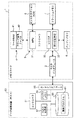
図1は、本発明の実施形態におけるメモリカード及びデータ処理装置(以下「ホスト」と称する。)の構成を示すブロック図である。 FIG. 1 is a block diagram showing a configuration of a memory card and a data processing apparatus (hereinafter referred to as “host”) in an embodiment of the present invention.
(ホストの構成)
ホスト(データ処理装置)50は、例えばディジタルスチルカメラ、ディジタルビデオカメラ、各種携帯端末機器、パーソナルコンピュータ等の電子機器を含む。
(Host configuration)
The host (data processing device) 50 includes electronic devices such as a digital still camera, a digital video camera, various portable terminal devices, and a personal computer.
ホスト50は、コントローラ51、データ格納部53、カードインタフェース55、入出力処理部57及びバッファメモリ59を含む。データ格納部53は制御プログラム61を格納する。
The
カードインタフェース55は、メモリカード1のホストインタフェース2との間でデータのやりとりを行う。すなわち、カードインタフェース55は、メモリカード1に読み書きするデータや各種制御のためのコマンドやクロック信号をホストインタフェース2との間で送受信する。
The
コントローラ51はホスト50全体の動作制御を行い、データ格納部53に格納されている制御プログラム61と協働して後述する所定の機能を実現する。
The
入出力処理部57は、ユーザがホスト50に対して行う設定や操作に関する情報やデータを入力する入力手段と、映像、音声等の出力を行う出力手段とを含む。
The input /
バッファメモリ59は、メモリカード1に書き込むデータを一時的に格納するメモリであり、メモリカード1に書き込みエラーが発生した場合でも、そのエラーを吸収できるように、ある程度大きな容量を有している。
The
(メモリカードの構成)
メモリカード1はホスト50に装着されて使用され、ホスト50からデータの書き込み、読み出しが可能な記録媒体である。メモリカード1は、書き込み時にエラーが生じたときに再試行するリトライ機能と、データの誤り訂正を行う誤り訂正機能とを有する。
(Memory card configuration)
The
メモリカード1は、ホストインタフェース2と、コントローラ3と、RAM4と、インストラクションROM5と、バッファメモリ6と、書き換え可能な不揮発性メモリであるフラッシュメモリ7とから構成される。
The
ホストインタフェース2は、メモリカード1が装着されるホスト50とのインタフェースを行うブロックであり、フラッシュメモリ7に読み書きするデータや各種制御のためのコマンドやクロック信号を送受信する。
The
コントローラ3は、メモリカード1全体を制御するブロックであり、マイクロプロセッサ(以下、「MPU」と称する。)31と、レジスタ32と、誤り訂正手段33を有している。
The
MPU31は、インストラクションROM5に格納されている制御プログラムを実行し、RAM4、フラッシュメモリ7及びバッファメモリ6の制御を行う。
The
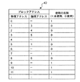
レジスタ32はメモリカード1に対する管理情報を保持する記憶手段である。管理情報には、ホストインタフェース2を通してホスト50から転送される設定値及びメモリカード1の固有の特性値が含まれる。図2にレジスタ32に格納される管理情報の例を示す。
The
図2において、管理情報は、ホスト50から転送される設定値として、リトライイネーブルビットと、誤り訂正イネーブルビットとを含む。リトライイネーブルビットは、メモリカード1においてデータ書き込み時にリトライ処理を実行するか否かを指定する「リトライ設定情報」である。訂正イネーブルビットは、メモリカード1においてデータ読み出し時に、誤り訂正処理を実行するか否かを指定する「誤り訂正設定情報」である。
In FIG. 2, the management information includes a retry enable bit and an error correction enable bit as setting values transferred from the
さらに、管理情報は、メモリカード1に固有の特性値として、データ書き込みの最大所要時間と、リトライ発生頻度と、エラー発生頻度と、誤り率とを保持している。データ書き込みの最大所要時間については、リトライ処理を行う場合と、行わない場合とのそれぞれについての値が格納されている。リトライ発生頻度は、リトライ処理が発生する頻度すなわち確率である。エラー発生頻度は、リトライ処理が行われない場合に、書き込み時にエラーが発生する頻度すなわち確率である。誤り率については、誤り訂正処理を行う場合と、行わない場合とのそれぞれについての値が格納されている。何れの情報もホストインタフェース2を通してホスト50から読み出すことが可能である。なお、メモリカード固有の特性値として管理情報に格納される情報には、上記以外に、メモリ種別、消去ブロックサイズ、管理ブロックサイズ、使用温度条件、消費電力等が含まれてもよい。
Further, the management information holds the maximum required time for data writing, the retry occurrence frequency, the error occurrence frequency, and the error rate as characteristic values unique to the
図1に戻り、誤り訂正手段33は、データ書き込み時に、ホスト50から転送されたデータに対して、誤り訂正符号を生成して、付加し、さらに、データ読み出し時に、フラッシュメモリ7から読み出したデータに誤りがあるか否かを検出し、誤りがある場合には訂正処理を行う。
Returning to FIG. 1, the error correction means 33 generates and adds an error correction code to the data transferred from the
インストラクションROM5は、読み出し専用の不揮発性メモリであり、MPU31の制御プログラムが格納されている。バッファメモリ6は、ホストから転送されてきたデータを一時的に保持する。フラッシュメモリ7は、ホストから転送されたデータを格納する。
The
RAM4は揮発性メモリであり、コントローラ3の作業用領域であるワークRAM41と、ブロック管理テーブル42とから構成されている。ブロック管理テーブル42はフラッシュメモリ7の使用状態を管理するテーブルである。図3に、ブロック管理テーブル42の一例を示す。
The
一般にフラッシュメモリ7の物理的なブロック(以下「物理ブロック」と称す。)への読み書きは、ホスト50から与えられる論理的なブロック(以下「論理ブロック」と称す。)のアドレスを指定して行われる。ブロック管理テーブル42の1つの役割は、論理ブロックのアドレス(論理アドレス)を物理ブロックのアドレス(物理アドレス)に変換する(あるいは、割り当てる)ことである。
In general, reading and writing to a physical block (hereinafter referred to as “physical block”) of the
図3のブロック管理テーブル42は、ブロックアドレスである物理アドレスと論理アドレスの対応関係と、その物理アドレス(すなわち、その物理アドレスが指定するブロック)の使用の有無を管理している。 The block management table 42 in FIG. 3 manages the correspondence between a physical address and a logical address, which are block addresses, and whether or not the physical address (that is, the block specified by the physical address) is used.
例えば、図3に示すように、物理ブロックの使用の有無、及び各物理ブロックに割り当てられた論理アドレスの番号が書かれている。使用済み(使用の有無を示す欄の値が“0”)であるにもかかわらず、論理アドレスが書かれていない物理アドレス(図2の例では、物理アドレス「6」)が指定する物理ブロックは、その物理ブロックが不良ブロックであることを意味しており、書き込みアドレスとして選択されることはない。 For example, as shown in FIG. 3, the presence / absence of use of a physical block and the number of a logical address assigned to each physical block are written. A physical block designated by a physical address (in the example of FIG. 2, physical address “6”) in which a logical address is not written even though it has been used (the value in the column indicating whether or not used is “0”) Means that the physical block is a bad block and is not selected as a write address.
(ホスト側の処理)
図4に示すフローチャートを参照し、ホスト50がメモリカード1の初期化時に行う処理について説明する。図4に示す処理は、ホスト50のコントローラ51により実行され、メモリカード1がホスト50に新たに装着されたときや、メモリカード1が装着された状態でホスト50の電源が投入された時等に実行される。
(Host side processing)
With reference to the flowchart shown in FIG. 4, processing performed by the
最初に、コントローラ51はメモリカード1に対し、メモリカード1を初期化するためのコマンドを発行する(S51)。メモリカード1はこのコマンドを受けると、所定の初期化処理を実行する。次に、コントローラ51は、メモリカード1において初期化処理の完了を確認するためのコマンドをメモリカード1に発行する(S52)。メモリカード1はこのコマンドを受けると、初期化処理が完了したか否かを示す応答をホスト50に送信する。コントローラ51はメモリカード1からの応答を受け、初期化処理の完了を判断する(S53)。
First, the
初期化処理が完了していれば(ステップS53でYES)、コントローラ51はメモリカード1に対して、「リトライ発生頻度」と、「エラー発生頻度」と、リトライ処理を行う場合と行わない場合のそれぞれに対する「書き込み時間の最大所要時間」とを要求する(S54)。この要求にしたがい、メモリカード1は、レジスタ32に格納されているそれらの情報をホスト50に送信する。コントローラ51は、メモリカード1から受信した情報にしたがい、メモリカード1の使用の可否を判断する(S55)。この判断は例えば以下のように行う。
If the initialization process has been completed (YES in step S53), the
すなわち、データ処理装置50はメモリカード1に書き込みエラーが発生してもある程度は許容できるようにバッファメモリ59を搭載している。コントローラ51は、メモリカード1から受信した情報にもとづき得られる判定条件がバッファメモリ59の許容量を超えるか否かに基づき、メモリカード1の使用の可否を判断する。判定条件として以下の2点を考慮する。
判定条件1: リトライ発生頻度×リトライ処理を行う場合の書き込み時間の最大所要時間
判定条件2: エラー発生頻度×リトライ処理を行わない場合の書き込み時間の最大所要時間
In other words, the
Judgment condition 1: Retry occurrence frequency × maximum required time of write time when retry process is performed Judgment condition 2: Error occurrence frequency × maximum required time of write time when retry process is not performed
コントローラ51は、上記の判定条件1、2が双方とも基準値を超える場合は、バッファメモリ59の許容量を超え、システムとして破綻すると判断し、メモリカード1は使用不可であると判断する。判定条件1、2の少なくともいずれかが基準値内であれば、メモリカード1は使用可能であると判断する。メモリカード1が使用不可能であると判断された場合(ステップS55でNO)、エラーとして処理し(S63)、処理を終了する。
If both of the
一方、メモリカード1が使用可能であると判断された場合(ステップS55でYES)、コントローラ1は、判定条件1に基づいて、さらにメモリカード1のリトライ機能を作動させるか、停止させるかについて判断する(S56)。すなわち、判定条件1を、リトライ機能の作動/停止を判断するための基準値と比較し、判定条件1がその基準値よりも大きい場合、メモリカード1のリトライ機能を停止させるようにする。これは、書き込み時間の最大所要時間が大きいと、ホスト50が動画記録等のリアルタイム処理を要求する場合に、リトライ処理の実行によりデータ記録に時間がかかり、リアルタイム処理が実現できない場合があるからである。
On the other hand, when it is determined that the
このように、ホスト50はメモリカード1のリトライ機能のON/OFFを設定できるため、リトライ機能が不要な場合はOFFすることで、書き込み時間の見積もり等が容易になる。すなわち、書き込みエラー時に、リトライ処理を実施せず、速やかにホスト50に通知されるようにすることにより、ホスト50側での対処が容易となる。
As described above, the
リトライ機能を停止させると判断した場合(ステップS57でYES)、コントローラ51は、メモリカード1に対し、レジスタ32内のリトライイネーブルビットをOFFに設定するためのコマンドを発行する(S58)。メモリカード1はこのコマンドを受けると、レジスタ32内のリトライイネーブルビットをOFFに設定する。
If it is determined that the retry function is to be stopped (YES in step S57), the
次に、コントローラ51は、メモリカード1に対し、誤り訂正を行う場合と行わない場合のそれぞれについての誤り率を要求する(S59)。
Next, the
そして、受信した誤り訂正を行わない場合の誤り率に基づいてメモリカード1の使用の可否を判断する(S60)。例えば、メモリカード1の誤り訂正を行わない場合の誤り率が非常に高く、ホスト側の誤り訂正機能を用いても訂正不能で、許容できるデータ品質が得られないと考えられる場合は、メモリカード1は使用不可能であると判断する。具体的には、メモリカード1の誤り訂正を行わない場合の誤り率を、所定の基準値(第1の基準値)と比較し、そのメモリカード1の誤り率が、第1の基準値よりも大きい場合、そのメモリカード1は使用不可能であると判断する。なお、第1の基準値は、ホスト50側で訂正可能な誤り率よりも高い値に設定する。
Then, based on the error rate when the received error correction is not performed, it is determined whether or not the
メモリカード1が使用不可能であると判断した場合(ステップS60でNO)、エラーとして処理し(S63)、処理を終了する。
If it is determined that the
メモリカード1が使用可能であると判断した場合(ステップS60でYES)、コントローラ1は、メモリカード1の誤り訂正を行う場合の誤り率に基づいて、メモリカード1の誤り訂正機能を作動させるか、停止させるかについて判断する(S61)。メモリカード1は使用可能であると判断されるが、メモリカード1の誤り訂正機能では十分なデータ品質が得られないと判断される場合は、ホスト50側で誤り訂正を実行する。このため、メモリカード1の誤り訂正機能を停止させる。具体的には、誤り訂正を行う場合のメモリカード1の誤り率が、訂正機能の作動/停止を判断するための基準値(第2の基準値、第2の基準値<第1の基準値)より大きいときは、メモリカード1において誤り訂正機能を停止させるようにする。
If it is determined that the
メモリカード1の誤り訂正機能を停止させると判断した場合(ステップS61でYES)、コントローラ51は、メモリカード1に対し、レジスタ32内の誤り訂正イネーブルビットをOFFに設定するためのコマンドを発行する(S62)。メモリカード1はこのコマンドを受けると、レジスタ32内の誤り訂正イネーブルビットをOFFに設定する。
If it is determined to stop the error correction function of the memory card 1 (YES in step S61), the
このように、ホスト側からメモリカード1の誤り訂正機能のON/OFFを設定できる。このため、高い誤り訂正能力を有するホスト50は、メモリカード1の誤り訂正能力が要求する能力より低いと判断したときは、メモリカード1の誤り訂正機能を停止させ、ホスト側で誤り訂正することが可能となり、これによりデータ信頼性を向上できる。
Thus, ON / OFF of the error correction function of the
以上のように、ホスト50は、メモリカード1の初期化処理時において、メモリカード1からそのメモリカードに固有の特性値を読み出し、その特性値に基づき、必要に応じてメモリカード1のリトライ機能及び誤り訂正機能のON/OFFを設定することができる。
As described above, the
(データ書き込み処理)
メモリカード1のデータ書き込み処理について、図5に示すフローチャートを参照して説明する。図5に示すフローチャートは、メモリカード1のコントローラ3により実行される。また、本処理はメモリカード1がホスト50から書き込みコマンドを受信したときに開始される。なお、以下では説明の便宜上、フラッシュメモリ7におけるデータ書き込み単位であるページとデータ消去単位であるブロックとを同じサイズに設定している。よって、データはブロック単位で書き込まれる。
(Data writing process)
The data writing process of the
まず、MPU31は、ホストインタフェース2を介して、ホスト50から書き込みコマンドを受信すると、ホスト50から送られてくる書き込みデータをバッファメモリ6に一時的に格納する(S1)。
First, when receiving a write command from the
次に、MPU31は、図3に示すブロック管理テーブル42に書き込まれている情報を参照し、書き込み可能な物理アドレスすなわち未使用(”1”)の物理アドレスをサーチして求める(S2)。
Next, the
次に、バッファメモリ6からブロック単位でデータを読み出すとともに、誤り訂正手段33によって誤り訂正符号を付加し、フラッシュメモリ7内のレジスタへデータを転送する(S3)。
Next, data is read out from the
次に、フラッシュメモリ7に対して書き込みコマンドを発行し、サーチした物理アドレスにデータの書き込みを行う(S4)。書き込み動作後、フラッシュメモリ7においてデータ書き込みの処理ステータスが正常であるか否かを判断する(S5)。そのため、フラッシュメモリ7に対してステータスリードコマンドを発行し、フラッシュメモリ7においてデータ書き込みが正常に完了したか否かを示す状態をフラッシュメモリ7から取得する。ステータスリードにおいて、エラーが返信される場合としては、書き込みエラーに加えて、フラッシュメモリに特有のイレース処理による異常終了した場合等が含まれる。
Next, a write command is issued to the
MPU31は、フラッシュメモリ7からのステータスリードコマンドに対する応答により、データ書き込みが正常に行われたと判断した場合(ステップS5でYES)、ブロック管理テーブル42上の対応するアドレスについて、使用の有無に関する情報を未使用“1”から使用“0”に書き換え、それとともに、論理アドレス(論理ブロック番号)を書き込み(S6)、書き込み処理を正常終了する(S7)。書き込み処理が正常終了すると、その旨がホスト50に通知される。
When the
一方、ステップS5において、データ書き込みが正常に行われなかったと判断された場合(ステップS5でNO)、データ書き込みを行ったアドレスに関し、ブロック管理テーブル42上の使用の有無に関する管理情報を未使用“1”から使用“0”に書き換える(S8)。 On the other hand, if it is determined in step S5 that the data writing has not been performed normally (NO in step S5), the management information regarding the presence / absence of use on the block management table 42 is not used for the address where the data is written. It is rewritten from “1” to use “0” (S8).
次に、レジスタ32に保持されたリトライイネーブルビットを参照し、その値が、ON(イネーブル(enable))かOFF(ディセーブル(disable))かを判断する(S9)。
Next, referring to the retry enable bit held in the
リトライイネーブルビットがOFFのとき(ステップS9でNO)、これはリトライ機能の停止を意味することから、リトライ処理を実行せずに、所定のエラー処理を実行後(S11)、処理を終了する。所定のエラー処理は、例えば、ホスト50へエラーの発生を通知する。この場合、ブロック管理テーブル42への論理アドレスの書き込みは行われない。すなわち、その物理アドレスは不良ブロックとなる。
When the retry enable bit is OFF (NO in step S9), this means that the retry function is stopped. Therefore, after executing a predetermined error process without executing the retry process (S11), the process is terminated. For example, the predetermined error process notifies the
一方、リトライイネーブルビットがON(イネーブル)のとき(ステップS9でYES)、その書き込み処理がリトライ処理(2回目の処理)であるか否かを判断する(S10)。リトライ処理であると判断された場合、所定のエラー処理を実行後(S11)、処理を終了する。この場合、ブロック管理テーブル42への論理アドレスの書き込みは行われない。すなわち、その物理アドレスは不良ブロックとなる。 On the other hand, when the retry enable bit is ON (enabled) (YES in step S9), it is determined whether or not the writing process is a retry process (second process) (S10). If it is determined that the process is a retry process, a predetermined error process is executed (S11), and the process ends. In this case, the logical address is not written to the block management table 42. That is, the physical address becomes a bad block.
ステップS10においてリトライ処理でなかった場合は、リトライ処理を実行するためにステップS12に進む。ステップS12においては、ステップS2と同様に、ブロック管理テーブル42を参照し、書き込み可能な物理アドレスすなわち未使用(“1”)の物理アドレスをサーチして決定した後、ステップS4に移行する。その後の処理は前述したとおりである。 If it is not the retry process in step S10, the process proceeds to step S12 to execute the retry process. In step S12, as in step S2, the block management table 42 is referred to and a writable physical address, that is, an unused (“1”) physical address is searched and determined. Then, the process proceeds to step S4. Subsequent processing is as described above.
以上のような手順にしたがい、バッファメモリ6に保持されたデータはブロック単位でフラッシュメモリ7への書き込み(転送)が繰り返され、全てのデータの書き込みが正常終了した時点で、書き込みが完了したことがホスト50に通知される。また、データ書き込み時に異常が発生した場合、リトライ機能がOFFであれば、それ以降のデータの書き込みは行われず、異常発生時点で、ホスト50に通知される。
According to the above procedure, the data held in the
以上のように本実施の形態によれば、ステップS9において、リトライイネーブルビットがイネーブルの場合(ステップS9でYES)にのみ、リトライ処理が実施される。このため、ホスト50からリトライイネーブルビットをOFF(ディセーブル)に設定しておくことで、書き込み異常があった場合に、リトライ処理を待たずに、異常がホスト50に通知されるようにすることができる。更に、事前にレジスタ32から読み出した、書き込み時間の最大所要時間、リトライ発生頻度を参照することで、それらの値に応じたエラー処理をホスト50側で実施することができる。
As described above, according to the present embodiment, in step S9, the retry process is performed only when the retry enable bit is enabled (YES in step S9). Therefore, by setting the retry enable bit to OFF (disabled) from the
なお、上記実施の形態では、リトライ処理時に書き込みデータをホスト50から再度転送しない場合について説明したが、書き込みデータを再度転送するようにしても良い。
In the above embodiment, the case where the write data is not transferred again from the
(データ読み出し処理)
次にメモリカード1のデータ読み出し処理について、図6に示すフローチャートを参照して説明する。図6に示される処理は、コントローラ3により実行されるものである。また、本処理はメモリカード1がホスト50から読み出しコマンドを受信したときに開始される。
(Data read processing)
Next, the data reading process of the
コントローラ3は、ホストインタフェース2を介してホスト50から読み出しコマンドを受信すると、MPU31はブロック管理テーブル42に書き込まれている情報を参照し、ホスト50から読み出しアドレスとして指定された論理アドレスに対応する物理アドレスをサーチして求める(S21)。
When the
次に、サーチした物理アドレスが指定するブロックからデータの読み出しを行う(S22)。このため、MPU31はフラッシュメモリ7に対して読み出しコマンドを発行し、これにより、フラッシュメモリ7内のレジスタに読み出したデータが保持される。
Next, data is read from the block designated by the searched physical address (S22). For this reason, the
次に、フラッシュメモリ7のレジスタからデータが読み出され、誤り訂正手段33を経由して誤りが検出された後、バッファメモリ6に転送され、一時的に格納される(S23)。
Next, data is read from the register of the
次に、レジスタ32に保持された誤り訂正イネーブルビットがON(イネーブル)か否かを判断する(S24)。誤り訂正イネーブルビットがON(イネーブル)すなわち誤り訂正処理をする場合(ステップS24でYES)は、誤りが検出されたか否かを判断する(S25)。誤りが検出されていない場合(ステップS25でNO)、正常終了する。誤りが検出された場合(ステップS25でYES)は、誤りの位置、大きさを算出し(S26)、それらの情報に基づいて誤り訂正可能か否かを判断する(S27)。
Next, it is determined whether or not the error correction enable bit held in the
ステップS27において、検出された誤りがメモリカード1の誤り訂正能力以内の場合、バッファメモリ6に保持されたデータの訂正を行い(S28)、正常終了する(S29)。検出された誤りがメモリカード1の訂正能力を超えており、訂正不能と判断した場合(ステップS27でNO)、異常終了する(ステップS30)。
If the detected error is within the error correction capability of the
また、誤り訂正イネーブルビットがOFF(ディセーブル)の場合(ステップS24でNO)、誤り訂正を行うことなく正常終了する(S29)。 If the error correction enable bit is OFF (disabled) (NO in step S24), the process ends normally without error correction (S29).
正常終了(S29)の場合、フラッシュメモリ7からバッファメモリ6へのブロック単位の読み出しが繰り返され、バッファメモリ6上のデータがホストインタフェース2を通してホスト50へ転送される。異常終了(S30)の場合、その旨がホスト50に通知され、異常発生後のフラッシュメモリ7からのデータの読み出しは停止する。
In the case of normal termination (S29), the block unit reading from the
以上のように本実施の形態によれば、ステップS24において、誤り訂正イネーブルビットがイネーブル(ON)の場合のみ誤り訂正処理を行うため、誤り訂正イネーブルビットをディセーブルにしておくことで、たとえ、データの読み出し時に訂正能力を超える誤りがあったとしても、フラッシュメモリ7内の全てのデータを読み出し、出力することが可能となる。
As described above, according to the present embodiment, in step S24, error correction processing is performed only when the error correction enable bit is enabled (ON). Therefore, by disabling the error correction enable bit, Even if there is an error exceeding the correction capability at the time of reading data, all the data in the
つまり、ホスト50は、レジスタ32から誤り訂正処理を行う場合の誤り率を予め読み出し、それに基づいて誤り訂正イネーブルビットの設定を決定することで、メモリカード1における誤り訂正機能が不要な場合は、その機能を停止させることが可能となる。例えば、ホスト50がメモリカード1よりも強力な誤り訂正機能を有し、かつ、高いデータ信頼性を望む場合は、誤り訂正イネーブルビットをディセーブル(OFF)に設定し、誤り訂正機能を停止させておくことで、データの書き込み時には、ホスト側で強力な誤り訂正符号を付加した後、データの書き込みを行うことが可能となり、また、データ読み出し時には、ホスト側で誤り訂正を行うことが可能となり、これにより、データアクセス時の誤り率を低下させることが可能となる。
That is, the
なお、上記実施の形態では、不揮発性メモリを搭載したメモリカードに実施した場合について説明したが、その他、例えば電子機器が内蔵する不揮発性メモリに対しても、同様に実施可能であり、本発明の思想の適用はメモリカードに限られるものではないことは言うまでもない。 In the above-described embodiment, the case where the present invention is applied to a memory card equipped with a nonvolatile memory has been described. However, the present invention can be similarly applied to, for example, a nonvolatile memory built in an electronic device. Needless to say, application of this idea is not limited to memory cards.
本発明は、リトライ処理または誤り訂正処理を実施可能なメモリカードや、そのようなメモリカードに対してアクセスするデータ処理装置に適用できる。特に、本発明は、リトライ処理または誤り訂正処理が可能なメモリカードにおいて、ホスト側から必要に応じて、メモリカードにおけるリトライ処理または誤り訂正処理の作動/停止の設定を可能とするため、高い処理能力を有し、メモリカード側の能力に頼らないデータ処理装置(ホスト)及びそれに接続するメモリカードに有用である。 The present invention can be applied to a memory card that can perform a retry process or an error correction process, and a data processing apparatus that accesses such a memory card. In particular, according to the present invention, in a memory card capable of retry processing or error correction processing, it is possible to set operation / stop of retry processing or error correction processing in the memory card as necessary from the host side. This is useful for a data processing device (host) that has the capability and does not depend on the capability on the memory card side, and a memory card connected thereto.
なお、本発明は、特定の実施形態について説明されてきたが、当業者にとっては他の多くの変形例、修正、他の利用が明らかである。それゆえ、本発明は、ここでの特定の開示に限定されず、添付の請求の範囲によってのみ限定され得る。本出願は日本国特許出願、特願2004−026413号(2004年2月3日提出)に関連し、それらの内容は参照することにより本文中に組み入れられる。 While the present invention has been described with respect to particular embodiments, many other variations, modifications, and other uses will be apparent to those skilled in the art. Accordingly, the invention is not limited to the specific disclosure herein, but can be limited only by the scope of the appended claims. This application is related to Japanese Patent Application No. 2004-026413 (filed on Feb. 3, 2004), the contents of which are incorporated herein by reference.
1 メモリカード
2 ホストインタフェース
3 コントローラ
4 RAM
5 インストラクションROM
6 バッファメモリ
7 フラッシュメモリ
31 マイクロプロセッサ(MPU)
32 レジスタ
33 誤り訂正手段
41 ワークRAM
42 ブロック管理テーブル
50 ホスト(データ処理装置)
51 コントローラ
53 データ格納部
55 カードインタフェース
57 入出力処理部
59 バッファメモリ
1
5 Instruction ROM
6
32
42 Block management table 50 Host (data processing device)
51
Claims (5)
データ処理装置との間でコマンドやデータの送受信を行うホストインタフェースと、
データを格納する不揮発性メモリと、
メモリカードの動作を制御するコントローラと、
所定の管理情報を格納する記憶手段とを備え、
前記管理情報は、不揮発性メモリからのデータの読み出し時に誤り訂正機能を実行するか否かを指定するための誤り訂正設定情報を含み、
前記コントローラは、データ読み出し動作時に、誤り訂正設定情報を参照し、誤り訂正設定情報が誤り訂正機能の停止を示す場合は、読み出したデータに対して誤り訂正を行わないように、また、誤り訂正設定情報が誤り訂正機能の作動を示す場合は、読み出したデータに対して誤り訂正を行うように、読み出し動作を制御する、
メモリカード。 A memory card capable of writing and reading data from a data processing device,
A host interface for sending and receiving commands and data to and from the data processing device;
Non-volatile memory for storing data;
A controller that controls the operation of the memory card;
Storage means for storing predetermined management information,
The management information includes error correction setting information for designating whether to execute an error correction function when reading data from the nonvolatile memory,
The controller refers to the error correction setting information during the data reading operation, and if the error correction setting information indicates that the error correction function is stopped, the controller does not perform error correction on the read data, and the error correction. When the setting information indicates the operation of the error correction function, the read operation is controlled so that error correction is performed on the read data.
Memory card.
請求項1記載のメモリカード。 The management information further includes characteristic information specific to the memory card, and the controller transmits the characteristic information to the data processing device in response to a request from the data processing device.
The memory card according to claim 1.
メモリカードとの間でコマンドやデータの送受信を行うカードインタフェースと、
データ処理装置の動作を制御するコントローラとを備え、
前記コントローラは、メモリカードがデータ処理装置に装着されたとき又はデータ処理装置の電源投入時に、メモリカードから特性情報を読み出し、読み出した特性情報に基づき、メモリカードにおいて誤り訂正機能を実行するか否かの判断を行い、その判断結果にしたがい、誤り訂正設定情報を設定するためのコマンドをカードインタフェースを介してメモリカードに送信する、
データ処理装置。 Error correction setting information for specifying whether or not to execute an error correction function during a read operation, which is a memory card that can read and write data and can perform error correction on the read data And a data processing device accessible to a memory card that stores characteristic information unique to the memory card as management information,
A card interface for sending and receiving commands and data to and from the memory card;
A controller for controlling the operation of the data processing device,
The controller reads the characteristic information from the memory card when the memory card is inserted into the data processing apparatus or when the data processing apparatus is turned on, and whether to execute the error correction function in the memory card based on the read characteristic information And according to the result of the determination, a command for setting error correction setting information is transmitted to the memory card via the card interface.
Data processing device.
データ読み出し動作時に、誤り訂正設定情報を参照し、
誤り訂正設定情報が誤り訂正機能の停止を示す場合は、読み出したデータに対して誤り訂正を行わず、
一方、誤り訂正設定情報が誤り訂正機能の作動を示す場合は、読み出したデータに対して誤り訂正を行う、
メモリカードの制御方法。 Error correction setting information for specifying whether or not to execute an error correction function during a read operation, which is a memory card that can write and read data and can perform error correction on the read data Is a memory card control method for storing as management information,
Refer to the error correction setting information during the data read operation.
When the error correction setting information indicates that the error correction function is stopped, error correction is not performed on the read data.
On the other hand, when the error correction setting information indicates the operation of the error correction function, error correction is performed on the read data.
Memory card control method.
前記メモリカードから特性情報を読み出し、読み出した特性情報に基づいて、メモリカードにおいて誤り訂正機能を実行するか否かの判断を行い、その判断結果にしたがい、誤り訂正設定情報を設定するためのコマンドをカードインタフェースを介してメモリカードに送信する、
メモリカードに対する設定方法。 Error correction setting information for specifying whether or not to execute an error correction function during a read operation, which is a memory card that can read and write data and can perform error correction on the read data And a setting method for the memory card that stores characteristic information unique to the memory card as management information,
A command for reading characteristic information from the memory card, determining whether or not to execute an error correction function in the memory card based on the read characteristic information, and setting error correction setting information according to the determination result To the memory card via the card interface,
Setting method for memory card.
Priority Applications (1)
| Application Number | Priority Date | Filing Date | Title |
|---|---|---|---|
| JP2010285813A JP5079868B2 (en) | 2004-02-03 | 2010-12-22 | Memory card, data processing device, memory card control method and setting method |
Applications Claiming Priority (3)
| Application Number | Priority Date | Filing Date | Title |
|---|---|---|---|
| JP2004026413 | 2004-02-03 | ||
| JP2004026413 | 2004-02-03 | ||
| JP2010285813A JP5079868B2 (en) | 2004-02-03 | 2010-12-22 | Memory card, data processing device, memory card control method and setting method |
Related Parent Applications (1)
| Application Number | Title | Priority Date | Filing Date |
|---|---|---|---|
| JP2005517700A Division JP4679370B2 (en) | 2004-02-03 | 2005-02-02 | Data processing apparatus and memory card setting method |
Publications (2)
| Publication Number | Publication Date |
|---|---|
| JP2011108252A true JP2011108252A (en) | 2011-06-02 |
| JP5079868B2 JP5079868B2 (en) | 2012-11-21 |
Family
ID=34835848
Family Applications (2)
| Application Number | Title | Priority Date | Filing Date |
|---|---|---|---|
| JP2005517700A Expired - Fee Related JP4679370B2 (en) | 2004-02-03 | 2005-02-02 | Data processing apparatus and memory card setting method |
| JP2010285813A Expired - Fee Related JP5079868B2 (en) | 2004-02-03 | 2010-12-22 | Memory card, data processing device, memory card control method and setting method |
Family Applications Before (1)
| Application Number | Title | Priority Date | Filing Date |
|---|---|---|---|
| JP2005517700A Expired - Fee Related JP4679370B2 (en) | 2004-02-03 | 2005-02-02 | Data processing apparatus and memory card setting method |
Country Status (4)
| Country | Link |
|---|---|
| US (1) | US7624298B2 (en) |
| JP (2) | JP4679370B2 (en) |
| CN (1) | CN100535933C (en) |
| WO (1) | WO2005076203A1 (en) |
Cited By (3)
| Publication number | Priority date | Publication date | Assignee | Title |
|---|---|---|---|---|
| JP2015518994A (en) * | 2012-06-07 | 2015-07-06 | マイクロン テクノロジー, インク. | Improved address bus integrity |
| US9323608B2 (en) | 2012-06-07 | 2016-04-26 | Micron Technology, Inc. | Integrity of a data bus |
| KR20190113080A (en) * | 2018-03-27 | 2019-10-08 | 삼성전자주식회사 | Memory system including memory module, memory module, and operating method of memory module |
Families Citing this family (27)
| Publication number | Priority date | Publication date | Assignee | Title |
|---|---|---|---|---|
| US8327068B2 (en) * | 2005-03-03 | 2012-12-04 | Panasonic Corporation | Memory module, memory controller, nonvolatile storage, nonvolatile storage system, and memory read/write method |
| US7831882B2 (en) | 2005-06-03 | 2010-11-09 | Rambus Inc. | Memory system with error detection and retry modes of operation |
| US9459960B2 (en) | 2005-06-03 | 2016-10-04 | Rambus Inc. | Controller device for use with electrically erasable programmable memory chip with error detection and retry modes of operation |
| US8291295B2 (en) | 2005-09-26 | 2012-10-16 | Sandisk Il Ltd. | NAND flash memory controller exporting a NAND interface |
| US20090277965A1 (en) * | 2005-10-28 | 2009-11-12 | Panasonic Corporation | Semiconductor memory card |
| US7562285B2 (en) | 2006-01-11 | 2009-07-14 | Rambus Inc. | Unidirectional error code transfer for a bidirectional data link |
| US8352805B2 (en) | 2006-05-18 | 2013-01-08 | Rambus Inc. | Memory error detection |
| US20070271495A1 (en) * | 2006-05-18 | 2007-11-22 | Ian Shaeffer | System to detect and identify errors in control information, read data and/or write data |
| US7809899B2 (en) * | 2007-05-29 | 2010-10-05 | Lsi Corporation | System for integrity protection for standard 2n-bit multiple sized memory devices |
| CN101354754B (en) * | 2007-07-26 | 2011-03-16 | 上海瀚银信息技术有限公司 | Intelligent memory card built-in with CPU IC and uses thereof |
| US8443260B2 (en) * | 2007-12-27 | 2013-05-14 | Sandisk Il Ltd. | Error correction in copy back memory operations |
| JP2009252036A (en) * | 2008-04-08 | 2009-10-29 | Panasonic Corp | Memory card |
| US9594679B2 (en) * | 2008-05-01 | 2017-03-14 | Sandisk Il Ltd. | Flash cache flushing method and system |
| WO2010137178A1 (en) | 2009-05-25 | 2010-12-02 | Hitachi,Ltd. | Storage subsystem |
| TWI416523B (en) * | 2009-06-10 | 2013-11-21 | Silicon Motion Inc | Method for writing fail retry for a non-volatile memory, non-volatile memory, controller, and memory card |
| US20110041005A1 (en) * | 2009-08-11 | 2011-02-17 | Selinger Robert D | Controller and Method for Providing Read Status and Spare Block Management Information in a Flash Memory System |
| TWI424435B (en) | 2009-08-31 | 2014-01-21 | Phison Electronics Corp | Method for giving program commands to flash memory chips, and controller and storage system using the same |
| CN102023811B (en) * | 2009-09-10 | 2012-11-28 | 群联电子股份有限公司 | Method for transmitting programming command to flash memory, controller and storage system |
| KR101279710B1 (en) * | 2011-04-01 | 2013-06-27 | 엘에스산전 주식회사 | Plc data log module and method for storing data in the same |
| US8656251B2 (en) * | 2011-09-02 | 2014-02-18 | Apple Inc. | Simultaneous data transfer and error control to reduce latency and improve throughput to a host |
| EP3425507B1 (en) * | 2012-12-21 | 2020-04-08 | Hewlett Packard Enterprise Development L.P. | Memory module having error correction logic |
| JP6184121B2 (en) * | 2013-02-08 | 2017-08-23 | 株式会社メガチップス | Storage device inspection system, storage device inspection method, and nonvolatile semiconductor storage device |
| CN103546638B (en) * | 2013-10-29 | 2016-02-03 | 广东欧珀移动通信有限公司 | A kind of flash memory cards fall card restoration methods and mobile terminal thereof |
| US11361839B2 (en) | 2018-03-26 | 2022-06-14 | Rambus Inc. | Command/address channel error detection |
| US10990463B2 (en) | 2018-03-27 | 2021-04-27 | Samsung Electronics Co., Ltd. | Semiconductor memory module and memory system including the same |
| US10691377B2 (en) | 2018-09-21 | 2020-06-23 | Micron Technology, Inc. | Adjusting scan event thresholds to mitigate memory errors |
| US11537464B2 (en) * | 2019-06-14 | 2022-12-27 | Micron Technology, Inc. | Host-based error correction |
Citations (2)
| Publication number | Priority date | Publication date | Assignee | Title |
|---|---|---|---|---|
| JPH01209552A (en) * | 1988-02-17 | 1989-08-23 | Hitachi Maxell Ltd | Semiconductor file memory device |
| JPH0728690A (en) * | 1993-07-14 | 1995-01-31 | Hitachi Ltd | Flash memory system |
Family Cites Families (14)
| Publication number | Priority date | Publication date | Assignee | Title |
|---|---|---|---|---|
| US4706190A (en) * | 1983-09-22 | 1987-11-10 | Digital Equipment Corporation | Retry mechanism for releasing control of a communications path in digital computer system |
| US5369532A (en) * | 1991-11-12 | 1994-11-29 | Storage Technology Corporation | Method and apparatus for managing data on rewritable media to define read/write operational status |
| US5828583A (en) * | 1992-08-21 | 1998-10-27 | Compaq Computer Corporation | Drive failure prediction techniques for disk drives |
| US6078520A (en) * | 1993-04-08 | 2000-06-20 | Hitachi, Ltd. | Flash memory control method and information processing system therewith |
| KR970008188B1 (en) * | 1993-04-08 | 1997-05-21 | 가부시끼가이샤 히다찌세이사꾸쇼 | Control method of flash memory and information processing apparatus using the same |
| JPH0714392A (en) | 1993-06-14 | 1995-01-17 | Toshiba Corp | Nonvolatile semiconductor memory and semiconductor disk device using the same |
| JP3576625B2 (en) | 1995-02-28 | 2004-10-13 | 株式会社東芝 | Data management method for flash memory card and data processing device using the data management method |
| JP3242890B2 (en) * | 1998-12-16 | 2001-12-25 | 株式会社ハギワラシスコム | Storage device |
| JP4031190B2 (en) | 2000-09-29 | 2008-01-09 | 株式会社東芝 | MEMORY CARD, NONVOLATILE MEMORY, NONVOLATILE MEMORY DATA WRITE METHOD AND DATA WRITE DEVICE |
| EP1354450A2 (en) * | 2001-01-17 | 2003-10-22 | Broadcom Corporation | System and method for a guaranteed delay jitter bound when scheduling bandwidth grants for voice calls via a cable network |
| US7076604B1 (en) * | 2002-12-24 | 2006-07-11 | Western Digital Technologies, Inc. | Disk drive employing a disk command data structure for tracking a write verify status of a write command |
| US7177989B1 (en) * | 2003-12-31 | 2007-02-13 | Intel Corporation | Retry of a device read transaction |
| US7360713B2 (en) * | 2004-09-24 | 2008-04-22 | Renesas Technology Corp. | Semiconductor device |
| JP2006209525A (en) * | 2005-01-28 | 2006-08-10 | Matsushita Electric Ind Co Ltd | Memory system |
-
2005
- 2005-02-02 WO PCT/JP2005/001496 patent/WO2005076203A1/en active Application Filing
- 2005-02-02 JP JP2005517700A patent/JP4679370B2/en not_active Expired - Fee Related
- 2005-02-02 CN CNB2005800039528A patent/CN100535933C/en not_active Expired - Fee Related
- 2005-02-02 US US10/597,650 patent/US7624298B2/en not_active Expired - Fee Related
-
2010
- 2010-12-22 JP JP2010285813A patent/JP5079868B2/en not_active Expired - Fee Related
Patent Citations (2)
| Publication number | Priority date | Publication date | Assignee | Title |
|---|---|---|---|---|
| JPH01209552A (en) * | 1988-02-17 | 1989-08-23 | Hitachi Maxell Ltd | Semiconductor file memory device |
| JPH0728690A (en) * | 1993-07-14 | 1995-01-31 | Hitachi Ltd | Flash memory system |
Cited By (6)
| Publication number | Priority date | Publication date | Assignee | Title |
|---|---|---|---|---|
| JP2015518994A (en) * | 2012-06-07 | 2015-07-06 | マイクロン テクノロジー, インク. | Improved address bus integrity |
| US9323608B2 (en) | 2012-06-07 | 2016-04-26 | Micron Technology, Inc. | Integrity of a data bus |
| US9557926B2 (en) | 2012-06-07 | 2017-01-31 | Micron Technology, Inc. | Integrity of an address bus |
| US9639422B2 (en) | 2012-06-07 | 2017-05-02 | Micron Technology, Inc. | Synchronized transfer of data and corresponding error correction data |
| US10152373B2 (en) | 2012-06-07 | 2018-12-11 | Micron Technology, Inc. | Methods of operating memory including receipt of ECC data |
| KR20190113080A (en) * | 2018-03-27 | 2019-10-08 | 삼성전자주식회사 | Memory system including memory module, memory module, and operating method of memory module |
Also Published As
| Publication number | Publication date |
|---|---|
| CN100535933C (en) | 2009-09-02 |
| JP4679370B2 (en) | 2011-04-27 |
| US7624298B2 (en) | 2009-11-24 |
| WO2005076203A1 (en) | 2005-08-18 |
| JPWO2005076203A1 (en) | 2007-10-18 |
| US20070186040A1 (en) | 2007-08-09 |
| JP5079868B2 (en) | 2012-11-21 |
| CN1914627A (en) | 2007-02-14 |
Similar Documents
| Publication | Publication Date | Title |
|---|---|---|
| JP5079868B2 (en) | Memory card, data processing device, memory card control method and setting method | |
| EP2162822B1 (en) | Emerging bad block detection | |
| US7280416B2 (en) | Nonvolatile memory system | |
| JP4110000B2 (en) | Storage device | |
| US20080049504A1 (en) | Memory Control Circuit, Nonvolatile Storage Apparatus, and Memory Control Method | |
| KR20190022987A (en) | Data storage device and operating method thereof | |
| US20150052415A1 (en) | Data storage device, operating method thereof and data processing system including the same | |
| US11138080B2 (en) | Apparatus and method for reducing cell disturb in an open block of a memory system during a recovery procedure | |
| US11068177B2 (en) | Data storage devices and data processing methods for shortening time required for a host device to wait for initialization of the data storage device | |
| US10083114B2 (en) | Data storage device and operating method thereof | |
| KR20160074025A (en) | Operating method for data storage device | |
| KR102444606B1 (en) | Data storage device and operating method thereof | |
| US8151136B2 (en) | Method and device for correcting code data error | |
| KR20170086840A (en) | Data storage device and operating method thereof | |
| JP2004220068A (en) | Memory card and method for writing data in memory | |
| TWI779046B (en) | A memory device and memory system including the same | |
| JP2009176147A (en) | Electronic equipment and method for determining permission of access to memory of electronic equipment | |
| US20210026736A1 (en) | Memory system re-performing access operation and operating method thereof | |
| US11392310B2 (en) | Memory system and controller | |
| US10628067B2 (en) | Memory system and operating method thereof | |
| US8627157B2 (en) | Storing apparatus | |
| KR20200019513A (en) | Controller, memory system and operating method thereof | |
| US20230214151A1 (en) | Memory system and operating method thereof | |
| JP3444988B2 (en) | Nonvolatile semiconductor disk device and control method therefor | |
| JP2010079371A (en) | Storage device and electronic equipment |
Legal Events
| Date | Code | Title | Description |
|---|---|---|---|
| A131 | Notification of reasons for refusal |
Free format text: JAPANESE INTERMEDIATE CODE: A131 Effective date: 20120605 |
|
| A521 | Request for written amendment filed |
Free format text: JAPANESE INTERMEDIATE CODE: A523 Effective date: 20120802 |
|
| TRDD | Decision of grant or rejection written | ||
| A01 | Written decision to grant a patent or to grant a registration (utility model) |
Free format text: JAPANESE INTERMEDIATE CODE: A01 Effective date: 20120821 |
|
| A01 | Written decision to grant a patent or to grant a registration (utility model) |
Free format text: JAPANESE INTERMEDIATE CODE: A01 |
|
| A61 | First payment of annual fees (during grant procedure) |
Free format text: JAPANESE INTERMEDIATE CODE: A61 Effective date: 20120829 |
|
| FPAY | Renewal fee payment (event date is renewal date of database) |
Free format text: PAYMENT UNTIL: 20150907 Year of fee payment: 3 |
|
| R150 | Certificate of patent or registration of utility model |
Free format text: JAPANESE INTERMEDIATE CODE: R150 |
|
| LAPS | Cancellation because of no payment of annual fees |