JP2011106951A - Electric field layer forming method, electric field layer forming device, and magnetic field measuring system - Google Patents
Electric field layer forming method, electric field layer forming device, and magnetic field measuring system Download PDFInfo
- Publication number
- JP2011106951A JP2011106951A JP2009261969A JP2009261969A JP2011106951A JP 2011106951 A JP2011106951 A JP 2011106951A JP 2009261969 A JP2009261969 A JP 2009261969A JP 2009261969 A JP2009261969 A JP 2009261969A JP 2011106951 A JP2011106951 A JP 2011106951A
- Authority
- JP
- Japan
- Prior art keywords
- electric field
- field layer
- layer forming
- cell
- wall portion
- Prior art date
- Legal status (The legal status is an assumption and is not a legal conclusion. Google has not performed a legal analysis and makes no representation as to the accuracy of the status listed.)
- Pending
Links
Images

Abstract
Description
本発明は、電界層形成方法、電界層形成装置および磁場計測システムに関する。 The present invention relates to an electric field layer forming method, an electric field layer forming apparatus, and a magnetic field measurement system.
光ポンピングを利用した測定装置においては、セルの内部空間に封入された媒体の原子がセルの内壁面に衝突すると、媒体の原子の原子スピンが緩和されてしまい、この結果、測定対象の検出感度が低下してしまう。そこで、特許文献1には、セルの内壁面に衝突した媒体の原子スピンを強制的に復帰させる事により、媒体の原子の原子スピンが緩和されてしまうことを抑制することを目的として、内壁面に非磁性物質がコーティングされたセルを光ポンピング磁束計に用いることが記載されている。 In a measurement device using optical pumping, when the atoms of the medium enclosed in the internal space of the cell collide with the inner wall surface of the cell, the atomic spin of the atoms of the medium is relaxed, resulting in the detection sensitivity of the measurement target. Will fall. Therefore, in Patent Document 1, for the purpose of suppressing the atomic spin of the atoms of the medium from being relaxed by forcibly returning the atomic spin of the medium colliding with the inner wall surface of the cell, the inner wall surface is disclosed. Describes the use of a cell coated with a non-magnetic material for an optical pumping magnetometer.
しかしながら、上記技術では、コーティングの状態が場所によって均一でないと、媒体の原子の原子スピンの緩和を抑制する効果を、場所によって均一に得ることができない。また、コーティングが経年変化してしまうので、媒体の原子の原子スピンの緩和を抑制する効果を、長期間継続して得ることができない。そこで、本発明は、上記課題を解決することで、光ポンピングを利用した測定装置が備えるセルの内部空間に封入された媒体の原子スピンの緩和を抑制する効果を、均一かつ長期間継続して得ることができる、電界層形成方法、電界層形成装置および磁場計測システムを提供するものである。 However, in the above technique, if the coating state is not uniform depending on the location, the effect of suppressing the relaxation of the atomic spin of the atoms in the medium cannot be obtained uniformly depending on the location. In addition, since the coating changes over time, the effect of suppressing the relaxation of the atomic spin of the atoms in the medium cannot be obtained continuously for a long time. Therefore, the present invention solves the above-mentioned problems, and maintains the effect of suppressing the relaxation of atomic spin of the medium enclosed in the internal space of the cell provided in the measuring device using optical pumping uniformly and for a long time. An electric field layer forming method, an electric field layer forming apparatus, and a magnetic field measurement system that can be obtained are provided.
上記課題を解決するため、本発明の第1の態様の電界層形成方法は、光ポンピングを利用した測定装置が備える内部空間を有するセルに対して、電界層形成用ビームを照射して、前記セルの壁部内に前記電界層形成用ビームを全反射させながら通過させることにより、前記壁部の前記内部空間側の表面を覆う電界層を形成することを特徴とする。係る構成によれば、セルの壁部の内部空間側の表面において、電界層形成用ビームの進行方向の全域に亘って均一な電界層を形成することができる。したがって、セルの内部空間に封入された媒体の原子の原子スピンの緩和を抑制する効果を、電界層形成用ビームの進行方向の全域に亘って得ることができる。また、経年変化の多い物理的なコーティングを施さずに、経年変化の少ない電界層を形成するため、電界層形成用ビームを照射し続けることで、媒体の原子の原子スピンの緩和を抑制する効果を、長期間継続して得ることができる。 In order to solve the above-described problem, the electric field layer forming method according to the first aspect of the present invention is configured to irradiate a cell having an internal space provided in a measuring apparatus using optical pumping with an electric field layer forming beam, An electric field layer that covers the surface of the wall portion on the inner space side is formed by allowing the electric field layer forming beam to pass through the wall portion of the cell while being totally reflected. According to such a configuration, a uniform electric field layer can be formed over the entire region in the traveling direction of the electric field layer forming beam on the surface of the cell wall on the inner space side. Therefore, the effect of suppressing the relaxation of the atomic spins of the atoms of the medium enclosed in the internal space of the cell can be obtained over the entire traveling direction of the electric field layer forming beam. In addition, the effect of suppressing the atomic spin relaxation of atoms in the medium by continuously irradiating the electric field layer forming beam to form the electric field layer with little secular change without applying physical coating with much secular change. Can be obtained continuously for a long period of time.
上記電界層形成方法において、前記壁部の端面において、前記壁部の端面を包含する面形状となる前記電界層形成用ビームを、前記壁部の端面に対して照射してもよい。係る構成によれば、セルの壁部の内部空間側の表面において、セルの壁部の周方向の全域に亘って均一な電界層を形成することができる。したがって、セルの内部空間に封入された媒体の原子の原子スピンの緩和を抑制する効果を、セルの壁部の周方向の全域に亘って得ることができる。 In the electric field layer forming method, the end surface of the wall portion may be irradiated with the electric field layer forming beam having a surface shape including the end surface of the wall portion at the end surface of the wall portion. According to such a configuration, a uniform electric field layer can be formed over the entire area in the circumferential direction of the cell wall on the surface of the cell wall on the inner space side. Therefore, the effect of suppressing the relaxation of the atomic spins of the atoms of the medium enclosed in the internal space of the cell can be obtained over the entire circumferential direction of the wall of the cell.
上記電界層形成方法において、前記測定装置が備える光ポンピングビーム照射装置が前記セルに照射する光ポンピングビームと同一の波長の前記電界層形成用ビームを、前記セルに対して照射してもよい。係る構成によれば、セルの壁部へ衝突した媒体の原子を、生成した電界層で励起し、強制的に原子スピンを復帰することができる。また、電界層形成用ビームの照射源と、光ポンピングビームの照射源とを共用することができるため、電界層形成用ビームの照射源にかかる部品コストを削減することができる。 In the electric field layer forming method, the electric field layer forming beam having the same wavelength as that of the optical pumping beam applied to the cell may be applied to the cell by the optical pumping beam irradiation device provided in the measuring device. According to such a configuration, atoms of the medium colliding with the cell wall can be excited by the generated electric field layer, and the atomic spin can be forcibly restored. In addition, since the irradiation source of the electric field layer forming beam and the irradiation source of the optical pumping beam can be shared, it is possible to reduce the cost of components related to the irradiation source of the electric field layer forming beam.
また、本発明の第2の態様の電界層形成装置は、光ポンピングを利用した測定装置が備える内部空間を有するセルに対して、電界層形成用ビームを照射して、前記セルの壁部内に前記電界層形成用ビームを全反射させながら通過させることにより、前記壁部の前記内部空間側の表面を覆う電界層を形成することを特徴とする。係る構成によれば、セルの壁部の内部空間側の表面において、電界層形成用ビームの進行方向の全域に亘って均一な電界層を形成することができる。したがって、セルの内部空間に封入された媒体の原子の原子スピンの緩和を抑制する効果を、電界層形成用ビームの進行方向の全域に亘って得ることができる。また、経年変化の多い物理的なコーティングを施さずに、経年変化の少ない電界層を形成するため、電界層形成用ビームを照射し続けることで、媒体の原子の原子スピンの緩和を抑制する効果を、長期間継続して得ることができる。 Moreover, the electric field layer forming apparatus according to the second aspect of the present invention irradiates a cell having an internal space provided in a measuring apparatus using optical pumping with an electric field layer forming beam, and enters the cell wall. An electric field layer that covers the surface of the wall portion on the inner space side is formed by allowing the electric field layer forming beam to pass through while being totally reflected. According to such a configuration, a uniform electric field layer can be formed over the entire region in the traveling direction of the electric field layer forming beam on the surface of the cell wall on the inner space side. Therefore, the effect of suppressing the relaxation of the atomic spins of the atoms of the medium enclosed in the internal space of the cell can be obtained over the entire traveling direction of the electric field layer forming beam. In addition, the effect of suppressing the atomic spin relaxation of atoms in the medium by continuously irradiating the electric field layer forming beam to form the electric field layer with little secular change without applying physical coating with much secular change. Can be obtained continuously for a long period of time.
また、本発明の第3の態様の磁場計測システムは、光ポンピングを利用した測定装置と、上記電界層形成装置とを備えることを特徴とする。係る構成によれば、セルの内部空間に封入された媒体の原子の原子スピンの緩和を抑制する効果を、均一かつ長期間継続して得ることができるため、均一かつ長期間安定した検出感度で、測定対象を測定することができる。 A magnetic field measurement system according to a third aspect of the present invention is characterized by including a measurement device using optical pumping and the electric field layer forming device. According to such a configuration, the effect of suppressing the relaxation of atomic spins of the atoms of the medium enclosed in the internal space of the cell can be obtained continuously for a long period of time. The measurement object can be measured.
上記磁場計測システムにおいて、前記測定装置は、複数の前記セルを有し、当該磁場計測システムは、前記複数のセルのそれぞれに対して、前記電界層形成装置が設けられていてもよい。係る構成によれば、測定装置が備える複数のセルのそれぞれに対して、セルの壁部の内部空間側の表面において、電界層形成用ビームの進行方向の全域に亘って均一な電界層を形成することができる。したがって、測定装置が備える複数のセルのそれぞれに対して、セルの内部空間に封入された媒体の原子の原子スピンの緩和を抑制する効果を、電界層形成用ビームの進行方向の全域に亘って得ることができる。また、経年変化の多い物理的なコーティングを施さずに、経年変化の少ない電界層を形成するため、測定装置が備える複数のセルのそれぞれに対して、電界層形成用ビームを照射し続けることで、測定装置が備える複数のセルのそれぞれに対して、媒体の原子の原子スピンの緩和を抑制する効果を、長期間継続して得ることができる。 In the magnetic field measurement system, the measurement device may include a plurality of the cells, and the magnetic field measurement system may include the electric field layer forming device for each of the plurality of cells. According to such a configuration, for each of the plurality of cells included in the measurement apparatus, a uniform electric field layer is formed over the entire area in the traveling direction of the electric field layer forming beam on the inner space side surface of the cell wall. can do. Therefore, for each of the plurality of cells included in the measurement apparatus, the effect of suppressing the relaxation of atomic spins of the atoms of the medium enclosed in the internal space of the cell is exerted over the entire traveling direction of the electric field layer forming beam. Obtainable. In addition, in order to form an electric field layer with little secular change without applying physical coating with much aging, it is possible to continue irradiating each of a plurality of cells included in the measuring device with an electric field layer forming beam. The effect of suppressing the relaxation of the atomic spin of the atoms of the medium can be continuously obtained for each of the plurality of cells included in the measuring apparatus.
上記磁場計測システムにおいて、前記測定装置は、複数の前記セルを有し、当該磁場計測システムは、前記電界層形成装置から出力された前記電界層形成用ビームを、複数の前記電界層形成用ビームに分岐し、前記複数のセルのそれぞれに対して、前記電界層形成用ビームを照射して、前記セルの壁部内に前記電界層形成用ビームを全反射させながら通過させる光スプリッターをさらに備えてもよい。係る構成によれば、測定装置が備える複数のセルのそれぞれに対して、セルの壁部の内部空間側の表面において、電界層形成用ビームの進行方向の全域に亘って均一な電界層を形成することができる。したがって、測定装置が備える複数のセルのそれぞれに対して、セルの内部空間に封入された媒体の原子の原子スピンの緩和を抑制する効果を、電界層形成用ビームの進行方向の全域に亘って得ることができる。また、経年変化の多い物理的なコーティングを施さずに、経年変化の少ない電界層を形成するため、測定装置が備える複数のセルのそれぞれに対して、電界層形成用ビームを照射し続けることで、測定装置が備える複数のセルのそれぞれに対して、媒体の原子の原子スピンの緩和を抑制する効果を、長期間継続して得ることができる。特に、電界層形成装置から出力された電界層形成用ビームを複数の電界層形成用ビームに分岐して、複数のセルに照射するので、複数のセルに照射される電界層形成用ビームのプロファイルのばらつきを容易に抑えることができる。また、複数のセルに照射される電界層形成用ビームのプロファイルを変更する場合、電界層形成装置から出力される電界層形成用ビームのプロファイルを変更すればよいため、複数のセルに照射される電界層形成用ビームのプロファイルを容易に変更することができる。 In the magnetic field measurement system, the measurement device includes a plurality of the cells, and the magnetic field measurement system uses the electric field layer formation beam output from the electric field layer formation device as a plurality of the electric field layer formation beams. And an optical splitter for irradiating each of the plurality of cells with the electric field layer forming beam and allowing the electric field layer forming beam to pass through the wall of the cell while being totally reflected. Also good. According to such a configuration, for each of the plurality of cells included in the measurement apparatus, a uniform electric field layer is formed over the entire area in the traveling direction of the electric field layer forming beam on the inner space side surface of the cell wall. can do. Therefore, for each of the plurality of cells included in the measurement apparatus, the effect of suppressing the relaxation of atomic spins of the atoms of the medium enclosed in the internal space of the cell is exerted over the entire traveling direction of the electric field layer forming beam. Obtainable. In addition, in order to form an electric field layer with little secular change without applying physical coating with much aging, it is possible to continue irradiating each of a plurality of cells included in the measuring device with an electric field layer forming beam. The effect of suppressing the relaxation of the atomic spin of the atoms of the medium can be continuously obtained for each of the plurality of cells included in the measuring apparatus. Particularly, since the electric field layer forming beam output from the electric field layer forming apparatus is branched into a plurality of electric field layer forming beams and irradiated to a plurality of cells, the profile of the electric field layer forming beam irradiated to the plurality of cells. Can be easily suppressed. In addition, when changing the profile of the electric field layer forming beam irradiated to a plurality of cells, it is only necessary to change the profile of the electric field layer forming beam output from the electric field layer forming apparatus. The profile of the electric field layer forming beam can be easily changed.
<第1実施例>
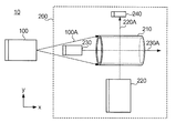
図1は、第1実施例に係る磁場計測システム10の構成を示す。磁場計測システム10は、測定対象の測定位置での磁場を計測する。たとえば、磁場計測システム10は、脳磁計、心磁計などの、数fT(フェムトテスラ)以下の非常に微弱な磁場を測定する生体計測システムに用いられる。磁場計測システム10は、光ポンピングを利用した測定装置である光ポンピング磁力計200を備える。光ポンピング磁力計200は、セル210、プローブ光照射装置220、光ポンピングビーム照射装置230、および検出装置240を有する。
<First embodiment>
FIG. 1 shows a configuration of a magnetic
セル210は、内部空間を有する筒形状を有する。図1に示す例では、セル210は、円筒形状を有している。セル210の内部空間には、媒体の一例としてアルカリ金属ガスの一つであるセシウムガスが封入されている。
The
光ポンピングビーム照射装置230は、セル210に対して光ポンピングビーム230Aを照射する。具体的には、光ポンピングビーム照射装置230は、セル210の内部空間に封入されている媒体の光ポンピングに適した波長の円偏光を、光ポンピングビーム230Aとしてx軸方向(セル210の中心軸方向)からセル210へ照射して、セル210の内部空間を通過させる。これにより、セル210の内部空間に封入されている媒体の原子が励起され、電子スピンの向きが揃えられる。
The optical pumping
プローブ光照射装置220は、セル210に対してプローブ光220Aを照射する。具体的には、プローブ光照射装置220は、セル210の内部空間に封入されている媒体の原子の電子スピンの向きが揃えられた状態で、直線偏光を、プローブ光220Aとしてy軸方向(x軸方向と直交する方向)からセル210へ照射して、セル210の内部空間を通過させる。セル210の内部空間を通過したプローブ光220Aは、測定対象の測定位置での磁場の強度に応じて、偏光面が回転される。
The probe
検出装置240は、セル210から出射されたプローブ光220Aから、測定対象の測定位置における磁場の強度を検出する。たとえば、検出装置240は、偏光板によって、セル210から出射されたプローブ光220Aから特定の回転角度の偏光を透過する。そして、検出装置240は、フォトダイオードによって、偏光板を透過した偏光の強度を検出する。さらに、検出装置240は、検出した偏光の強度および回転角度に基づいて、セル210から出射されたプローブ光220Aの偏光回転角を算出する。そのうえ、検出装置240は、検出された偏光回転角に基づいて、測定対象の測定位置における磁場の強度を算出する。
The
本実施形態の磁場計測システム10は、電界層形成装置100をさらに備える。電界層形成装置100は、セル210に対して、電界層形成用ビーム100Aを照射して、セル210の壁部内(セル210の壁部のうちのx軸方向に延伸する壁部内)に電界層形成用ビーム100Aを全反射させながら通過させることにより、セル210の壁部の内部空間側の表面を覆う電界層を形成する。具体的には、電界層形成装置100は、光ポンピングビーム230Aの波長と同一の波長の電界層形成用ビーム100Aをx軸方向からセル210の壁部の端面へ照射して、セル210の壁部内に電界層形成用ビーム100Aを全反射させながら通過させる。これにより、電界層形成装置100は、セル210の壁部の内部空間側の表面を覆う電界層であって、セル210に封入されている媒体の原子を励起する電界層を、セル210の壁部の内部空間側の表面における電界層形成用ビーム100Aの進行方向の全域に亘って均一に形成する。
The magnetic
電界層形成装置100は、セル210の壁部の端面において、セル210の壁部の端面を包含する面形状となる電界層形成用ビーム100Aを、セル210の壁部の端面に対して照射することで、セル210の壁部の内部空間側の表面において、セル210の壁部の周方向の全域に亘って均一な電界層を形成する。たとえば、電界層形成装置100は、セル210の壁部の端面において、セル210の壁部の端面の形状と同一の面形状となる電界層形成用ビーム100Aを、セル210の壁部の端面に対して照射する。図1に示す例では、セル210の壁部の端面は円形状を有しているので、電界層形成装置100は、セル210の壁部の端面において円形状となる電界層形成用ビーム100Aを、セル210の壁部の端面に対して照射する。このようにして、電界層形成装置100は、セル210の壁部の内部空間側の表面の全域に亘って、均一かつ経年変化の少ない電界層を効率的に形成する。
The electric field
セル210の壁部の内部空間側の表面が電界層で覆われることで、セル210の壁部へ向衝突した媒体の原子は、セル210の壁部の手前にある電界層で励起され、強制的に原子スピンが復帰される。このように、電界層形成装置100は、セル210の内壁面に対して、不均一かつ経年変化の多い物理的なコーティングを施さずに、均一かつ経年変化の少ない電界層を形成するため、媒体の原子の原子スピンの緩和を抑制する効果を、均一かつ長期間継続して得ることができる。
By covering the inner space side surface of the wall part of the
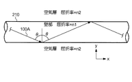
図2は、電界層形成用ビーム100Aの全反射条件を模式的に示す。電界層形成装置100は、以下の全反射条件(1)を満たす電界層形成用ビーム100Aを、セル210の壁部の端面に対して照射する。全反射条件(1)において、θcは臨界角を示す。また、n1は、セル210の壁部の屈折率を示す。また、n2は、セル210の壁部の表面に接する空気層の屈折率を示す。また、θは、セル210の壁部の表面に対する電界層形成用ビーム100Aの入射角を示す。このように、全反射条件を満たす電界層形成用ビーム100Aは、セル210の壁部内を全反射しながらセル210を通過する。この際に生じるエバネッセント波によって、セル210の壁部の両表面(内部空間側の表面および外部空間側の表面)を覆う電界層が形成される。
FIG. 2 schematically shows the total reflection conditions of the electric field
Sinθc=n2/n1(θ>θc)・・・(1) Sin θc = n2 / n1 (θ> θc) (1)
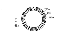
図3は、電界層が形成された状態のセル210の壁部の断面を示す。図3では、電界層が形成された状態のセル210の壁部を、電界層形成用ビーム100Aの進行方向であるx軸方向から見たときの断面を示す。電界層形成装置100は、セル210の壁部の端面において、セル210の壁部の周方向の全域に亘って、電界層形成用ビーム100Aを照射する。これにより、図3に示すように、セル210の壁部の両表面には、セル210の壁部の周方向の全域に亘って、セル210の壁部の表面を覆う電界層210Aが形成される。
FIG. 3 shows a cross-section of the wall of the
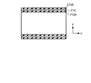
図4は、電界層が形成された状態のセル210の壁部の断面を示す。図4では、電界層が形成された状態のセル210壁部を、電界層形成用ビーム100Aの進行方向と直交する方向から見たときの断面を示す。電界層形成装置100は、セル210の壁部内を全反射しながらセル210を通過するための全反射条件を満たす電界層形成用ビーム100Aを、セル210の壁部の端面に対してx軸方向から照射する。電界層形成装置100から照射された電界層形成用ビーム100Aは、セル210の壁部内を全反射しながらセル210をx軸方向に通過する。これにより、図4に示すように、セル210の壁部の両表面には、x軸方向(電界層形成用ビーム100Aの進行方向)の全域に亘って、セル210の壁部の表面を覆う電界層210Aが形成される。
FIG. 4 shows a cross section of the wall portion of the
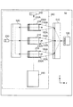
<第2実施例>
図5は、第2実施例に係る磁場計測システム10の構成を示す。図5に示す磁場計測システム10は、角筒形状のセル210が、プローブ光220Aの照射方向(y軸方向)に複数設けられており、複数のセル210のそれぞれに対して、光ポンピングビーム照射装置230と、電界層形成装置100とが設けられている点で、第1実施例で説明した磁場計測システム10と異なる。複数の電界層形成装置100のそれぞれは、第1実施例で説明した電界層形成装置100と同様に動作する。すなわち、複数の電界層形成装置100のそれぞれは、対応するセル210に電界層形成用ビーム100Aを照射することで、対応するセル210の壁部の表面に電界層を形成する。
<Second embodiment>
FIG. 5 shows a configuration of the magnetic
第2実施例に係る磁場計測システム10によれば、複数のセル210のそれぞれに対して、セル210の壁部の内部空間側の表面において、セル210の壁部の周方向の全域、および電界層形成用ビーム100Aの進行方向の全域に亘って、均一な電界層を形成することができる。したがって、複数のセル210のそれぞれに対して、セルの内部空間に封入された媒体の原子の原子スピンの緩和を抑制する効果を、セル210の壁部の周方向の全域、電界層形成用ビーム100Aの進行方向の全域に亘って得ることができる。また、複数のセル210のそれぞれに対して、経年変化の多い物理的なコーティングを施さずに、経年変化の少ない電界層を形成する。このため、複数のセル210のそれぞれに対して、電界層形成用ビーム100Aを照射し続けることで、媒体の原子の原子スピンの緩和を抑制する効果を、長期間継続して得ることができる。
According to the magnetic
なお、第2実施例に係る磁場計測システム10においては、セル210が1軸(y軸)方向に複数設けられているが、セル210が2軸方向に複数設けられてもよい。たとえば、複数のセル210が、x軸方向から見て格子状に並べて設けられてもよい。これらの場合も、複数のセル210の位置に対応して、複数の電界層形成装置100、および複数の光ポンピングビーム照射装置230を設け、複数のセル210のそれぞれに対して、第1実施例で説明した電界層形成装置100が照射する電界層形成用ビーム100Aと同条件の電界層形成用ビーム100Aを照射することで、複数のセル210のそれぞれの壁部の表面に電界層を形成することができる。
In the magnetic
<第3実施例>
図6は、第3実施例に係る磁場計測システム10の構成を示す。図6に示す磁場計測システム10は、複数の電界層形成装置100の代わりに、一の電界層形成装置100と、光スプリッター510とを備える点で、図5に示した磁場計測システム10と異なる。光スプリッター510は、電界層形成装置100から出力された電界層形成用ビーム100Aを、複数の電界層形成用ビーム100Aに分岐する。具体的には、光スプリッター510は、電界層形成装置100の位置に対応して設けられた入射口から入射された電界層形成用ビーム100Aを、セル210の数分の電界層形成用ビーム100Aに分岐する。複数の電界層形成用ビーム100Aのそれぞれは、対応するセル210の位置に対応して設けられた出射口から出射され、対応するセル210に対して照射される。
<Third embodiment>
FIG. 6 shows the configuration of the magnetic
光スプリッター510は、複数のセル210のそれぞれに対して、第1実施例で説明した電界層形成装置100と同様に、セル210の壁部内を全反射しながら通過する全反射条件を満たす電界層形成用ビーム100Aを、セル210の壁部の端面に対してx軸方向から照射する。すなわち、光スプリッター510は、複数のセル210のそれぞれに対して、第1実施例で説明した電界層形成装置100が照射する電界層形成用ビーム100Aと同条件の電界層形成用ビーム100Aを照射することで、セル210の壁部の内部空間側の表面に電界層を形成する。
As with the electric field
第3実施例に係る磁場計測システム10によれば、複数のセル210のそれぞれに対して、セル210の壁部の内部空間側の表面において、セル210の壁部の周方向の全域、および電界層形成用ビーム100Aの進行方向の全域に亘って、均一な電界層を形成することができる。したがって、複数のセル210のそれぞれに対して、セルの内部空間に封入された媒体の原子の原子スピンの緩和を抑制する効果を、セル210の壁部の周方向の全域、電界層形成用ビーム100Aの進行方向の全域に亘って得ることができる。また、複数のセル210のそれぞれに対して、経年変化の多い物理的なコーティングを施さずに、経年変化の少ない電界層を形成する。このため、複数のセル210のそれぞれに対して、電界層形成用ビーム100Aを照射し続けることで、媒体の原子の原子スピンの緩和を抑制する効果を、長期間継続して得ることができる。
According to the magnetic
特に、第3実施例に係る磁場計測システム10によれば、一の電界層形成装置100から出力された電界層形成用ビーム100Aを複数の電界層形成用ビーム100Aに分岐して、複数のセル210に照射するので、複数のセル210に照射される電界層形成用ビーム100Aのプロファイルのばらつきを容易に抑えることができる。また、複数のセル210に照射される電界層形成用ビーム100Aのプロファイルを変更する場合、電界層形成装置100から出力される電界層形成用ビーム100Aのプロファイルを変更すればよいため、複数のセル210に照射される電界層形成用ビーム100Aのプロファイルを容易に変更することができる。
In particular, according to the magnetic
図6に示す磁場計測システム10は、複数の光ポンピングビーム照射装置230の代わりに、一の光ポンピングビーム照射装置230と、光スプリッター520とを備える点でも、図5に示した磁場計測システム10と異なる。光スプリッター520は、光ポンピングビーム照射装置230から出力された光ポンピングビーム230Aを、複数の光ポンピングビーム230Aに分岐する。具体的には、光スプリッター520は、光ポンピングビーム照射装置230の位置に対応して設けられた入射口から入射された光ポンピングビーム230Aを、セル210の数分の光ポンピングビーム230Aに分岐する。複数の光ポンピングビーム230Aのそれぞれは、対応するセル210の位置に対応して設けられた出射口から出射され、対応するセル210に対して照射される。
The magnetic
第3実施例に係る磁場計測システム10によれば、一の光ポンピングビーム照射装置230から出力された光ポンピングビーム230Aを複数の光ポンピングビーム230Aに分岐して、複数のセル210に照射するので、複数のセル210に照射される光ポンピングビーム230Aのプロファイルのばらつきを容易に抑えることができる。また、複数のセル210に照射される光ポンピングビーム230Aのプロファイルを変更する場合、光ポンピングビーム照射装置230から出力される光ポンピングビーム230Aのプロファイルを変更すればよいため、複数のセル210に照射される光ポンピングビーム230Aのプロファイルを容易に変更することができる。
According to the magnetic
なお、第3実施例に係る磁場計測システム10においては、セル210が1軸(y軸)方向に複数設けられているが、セル210が2軸方向に複数設けられてもよい。たとえば、複数のセル210が、x軸方向から見て格子状に並べて設けられてもよい。これらの場合も、複数のセル210の位置に対応して、複数の電界層形成用ビーム100Aを照射する光スプリッター510、および複数の複数の光ポンピングビーム230Aを照射する光スプリッター520を設け、複数のセル210のそれぞれに対して、第1実施例で説明した電界層形成装置100が照射する電界層形成用ビーム100Aと同条件の電界層形成用ビーム100Aを照射することで、複数のセル210のそれぞれの壁部の表面に電界層を形成することができる。
In the magnetic
第3実施例に係る磁場計測システム10において、電界層形成装置100および光スプリッター510を複数備え、複数の電界層形成装置100および光スプリッター510によって、複数のセル210のそれぞれに対して、電界層形成用ビーム100Aを照射してもよい。また、光ポンピングビーム照射装置230および光スプリッター520を複数備え、複数の光ポンピングビーム照射装置230および光スプリッター520によって、複数のセル210のそれぞれに対して、光ポンピングビーム230Aを照射してもよい。
The magnetic
本実施形態の磁場計測システム10は、第1実施例−第3実施例で説明した構成に限らない。たとえば、磁場計測システム10は、磁場を計測するシステムであれば、生体計測システムに限らず、これ以外のシステムにも用いてもよい。また、電界層形成装置100は、セル210を挟んで、光ポンピングビーム照射装置230と対向して設けられていてよい。すなわち、セル210に対して、光ポンピングビーム230Aの照射方向の反対方向を、電界層形成用ビーム100Aの照射方向としてもよい。また、電界層形成装置100は、セル210の内部空間に封入されている媒体の光ポンピングに適した波長の円偏光であれば、光ポンピングビーム230Aの波長と異なる波長の電界層形成用ビーム100Aをセル210へ照射してもよい。
The magnetic
また、セル210は、円筒形状および角筒形状に限らず、セル210の壁部内に電界層形成用ビーム100Aを全反射させながら通過させることができるものであれば、円筒形状以外の形状を有してもよい。また、電界層形成装置100は、セル210の壁部の端面の形状に合わせて電界層形成用ビーム100Aの面形状を調整することができる調整機構を有していてもよい。また、セル210の内部空間に封入される媒体には、セシウムガスに限らず、これ以外の、カリウムガス、ルビジウムガスなどのアルカリ金属ガスを用いてもよい。また、セル210の内部空間に封入される媒体には、アルカリ金属ガスに限らず、これ以外の、希ガスなどの媒体を用いてもよい。また、電界層形成装置100は、セル210の内部空間に封入されている媒体に合わせて電界層形成用ビーム100Aの波長を調整することができる調整機構を有していてもよい。
The
10…磁場計測システム、100…電界層形成装置、100A…電界層形成用ビーム、200…光ポンピング磁力計、210…セル、210A…電界層、220…プローブ光照射装置、220A…プローブ光、230…光ポンピングビーム照射装置、230A…光ポンピングビーム、240…検出装置、510…光スプリッター、520…光スプリッター
DESCRIPTION OF
Claims (7)
ことを特徴とする電界層形成方法。 By irradiating a cell having an internal space provided in a measuring device using optical pumping with an electric field layer forming beam and passing the electric field layer forming beam through the wall of the cell while totally reflecting, A method of forming an electric field layer, comprising forming an electric field layer covering a surface of the wall portion on the inner space side.
ことを特徴とする請求項1に記載の電界層形成方法。 2. The electric field layer according to claim 1, wherein the electric field layer forming beam having a surface shape including the end surface of the wall portion is irradiated to the end surface of the wall portion at the end surface of the wall portion. Forming method.
ことを特徴とする請求項1または2に記載の電界層形成方法。 The optical pumping beam irradiation apparatus provided in the measurement apparatus irradiates the cell with the electric field layer forming beam having the same wavelength as the optical pumping beam applied to the cell. The electric field layer forming method as described.
ことを特徴とする電界層形成装置。 By irradiating a cell having an internal space provided in a measuring device using optical pumping with an electric field layer forming beam and passing the electric field layer forming beam through the wall of the cell while totally reflecting, An electric field layer forming apparatus, comprising: an electric field layer that covers a surface of the wall portion on the inner space side.
請求項4に記載の電界層形成装置と
を備えることを特徴とする磁場計測システム。 A measuring device using optical pumping;
A magnetic field measurement system comprising: the electric field layer forming apparatus according to claim 4.
複数の前記セルを有し、
当該磁場計測システムは、
前記複数のセルのそれぞれに対して、前記電界層形成装置が設けられている
ことを特徴とする請求項5に記載の磁場計測システム。 The measuring device is
Having a plurality of said cells;
The magnetic field measurement system
The magnetic field measurement system according to claim 5, wherein the electric field layer forming device is provided for each of the plurality of cells.
複数の前記セルを有し、
当該磁場計測システムは、
前記電界層形成装置から出力された前記電界層形成用ビームを、複数の前記電界層形成用ビームに分岐し、前記複数のセルのそれぞれに対して、前記電界層形成用ビームを照射して、前記セルの壁部内に前記電界層形成用ビームを全反射させながら通過させる光スプリッターをさらに備える
ことを特徴とする請求項5に記載の磁場計測システム。 The measuring device is
Having a plurality of said cells;
The magnetic field measurement system
The electric field layer forming beam output from the electric field layer forming apparatus is branched into a plurality of electric field layer forming beams, and each of the plurality of cells is irradiated with the electric field layer forming beam, The magnetic field measurement system according to claim 5, further comprising: an optical splitter that allows the electric field layer forming beam to pass through the wall of the cell while totally reflecting.
Priority Applications (1)
| Application Number | Priority Date | Filing Date | Title |
|---|---|---|---|
| JP2009261969A JP2011106951A (en) | 2009-11-17 | 2009-11-17 | Electric field layer forming method, electric field layer forming device, and magnetic field measuring system |
Applications Claiming Priority (1)
| Application Number | Priority Date | Filing Date | Title |
|---|---|---|---|
| JP2009261969A JP2011106951A (en) | 2009-11-17 | 2009-11-17 | Electric field layer forming method, electric field layer forming device, and magnetic field measuring system |
Publications (1)
| Publication Number | Publication Date |
|---|---|
| JP2011106951A true JP2011106951A (en) | 2011-06-02 |
Family
ID=44230598
Family Applications (1)
| Application Number | Title | Priority Date | Filing Date |
|---|---|---|---|
| JP2009261969A Pending JP2011106951A (en) | 2009-11-17 | 2009-11-17 | Electric field layer forming method, electric field layer forming device, and magnetic field measuring system |
Country Status (1)
| Country | Link |
|---|---|
| JP (1) | JP2011106951A (en) |
-
2009
- 2009-11-17 JP JP2009261969A patent/JP2011106951A/en active Pending
Similar Documents
| Publication | Publication Date | Title |
|---|---|---|
| Albisetti et al. | Optically inspired nanomagnonics with nonreciprocal spin waves in synthetic antiferromagnets | |
| WO2013008500A1 (en) | Magnetoencephalography meter and neuromagnetism measuring method | |
| JP6391370B2 (en) | Optical pumping magnetometer and magnetic sensing method | |
| Kwong et al. | Cooperative emission of a coherent superflash of light | |
| CN106018273B (en) | A kind of light beam transversal micro-displacement generation system based on light logic gates and mim structure | |
| WO2012120732A1 (en) | Optically pumped magnetometer, magnetoencephalography meter, and mri device | |
| Dai et al. | Ultrafast microscopy of spin-momentum-locked surface plasmon polaritons | |
| JP2009300108A (en) | Terahertz spectroscopic device | |
| Wang et al. | Complete polarization analysis of an APPLE II undulator using a soft X-ray polarimeter | |
| US20150205079A1 (en) | Terahertz band wavelength plate and terahertz wave measurement device | |
| Jia et al. | Direction-resolved radiation from polarization-controlled surface plasmon modes on silver nanowire antennas | |
| Bromberg et al. | Control of coherent backscattering by breaking optical reciprocity | |
| Hino et al. | Current status of BL06 beam line for VIN ROSE at J-PARC/MLF | |
| JP2011137687A (en) | Magnetic measuring apparatus | |
| JP5874808B2 (en) | Magnetic field measuring device | |
| JP2017215225A5 (en) | ||
| JP5900970B2 (en) | Surface plasmon sensor and method of measuring refractive index | |
| JP2011106950A (en) | Atom excitation layer forming method, atom excitation layer forming device, and magnetic field measuring system | |
| JP5914903B2 (en) | Magneto-optical effect measuring device | |
| JP2011106951A (en) | Electric field layer forming method, electric field layer forming device, and magnetic field measuring system | |
| Moriya et al. | Coherent backscattering of inelastic photons from atoms and their mirror images | |
| TW201643388A (en) | Radiation sensor apparatus | |
| Rehwald et al. | Tunable nanowires: An additional degree of freedom in plasmonics | |
| WO2011016378A1 (en) | Three-dimensional optical resonance device, polarized laser oscillation method, and polarized laser oscillation system | |
| KR102192983B1 (en) | Evaporating apparatus, method for mesuring evaporation speed using the same |