JP2011106950A - Atom excitation layer forming method, atom excitation layer forming device, and magnetic field measuring system - Google Patents
Atom excitation layer forming method, atom excitation layer forming device, and magnetic field measuring system Download PDFInfo
- Publication number
- JP2011106950A JP2011106950A JP2009261968A JP2009261968A JP2011106950A JP 2011106950 A JP2011106950 A JP 2011106950A JP 2009261968 A JP2009261968 A JP 2009261968A JP 2009261968 A JP2009261968 A JP 2009261968A JP 2011106950 A JP2011106950 A JP 2011106950A
- Authority
- JP
- Japan
- Prior art keywords
- excitation layer
- cell
- layer forming
- atomic excitation
- internal space
- Prior art date
- Legal status (The legal status is an assumption and is not a legal conclusion. Google has not performed a legal analysis and makes no representation as to the accuracy of the status listed.)
- Pending
Links
- 230000005284 excitation Effects 0.000 title claims abstract description 197
- 238000000034 method Methods 0.000 title claims description 10
- 210000004027 cell Anatomy 0.000 claims abstract description 180
- 230000003287 optical effect Effects 0.000 claims abstract description 76
- 238000005259 measurement Methods 0.000 claims abstract description 65
- 238000005086 pumping Methods 0.000 claims abstract description 57
- 210000002421 cell wall Anatomy 0.000 claims abstract description 13
- 230000001678 irradiating effect Effects 0.000 claims description 11
- 230000000694 effects Effects 0.000 abstract description 21
- 239000000523 sample Substances 0.000 description 12
- 239000011248 coating agent Substances 0.000 description 9
- 238000000576 coating method Methods 0.000 description 9
- 238000001514 detection method Methods 0.000 description 8
- 239000007789 gas Substances 0.000 description 8
- 230000015572 biosynthetic process Effects 0.000 description 4
- 230000010287 polarization Effects 0.000 description 4
- 229910052783 alkali metal Inorganic materials 0.000 description 3
- 150000001340 alkali metals Chemical class 0.000 description 3
- 230000032683 aging Effects 0.000 description 2
- 229910052792 caesium Inorganic materials 0.000 description 2
- TVFDJXOCXUVLDH-UHFFFAOYSA-N caesium atom Chemical compound [Cs] TVFDJXOCXUVLDH-UHFFFAOYSA-N 0.000 description 2
- 230000035945 sensitivity Effects 0.000 description 2
- ZLMJMSJWJFRBEC-UHFFFAOYSA-N Potassium Chemical compound [K] ZLMJMSJWJFRBEC-UHFFFAOYSA-N 0.000 description 1
- 239000000696 magnetic material Substances 0.000 description 1
- 239000012466 permeate Substances 0.000 description 1
- 229910052700 potassium Inorganic materials 0.000 description 1
- 239000011591 potassium Substances 0.000 description 1
- 229910052701 rubidium Inorganic materials 0.000 description 1
- IGLNJRXAVVLDKE-UHFFFAOYSA-N rubidium atom Chemical compound [Rb] IGLNJRXAVVLDKE-UHFFFAOYSA-N 0.000 description 1
Images

Landscapes
- Measuring Magnetic Variables (AREA)
- Measurement And Recording Of Electrical Phenomena And Electrical Characteristics Of The Living Body (AREA)
Abstract
【課題】光ポンピングを利用した測定装置が備えるセルに封入された媒体の原子スピンの緩和を抑制する効果を、場所によって均一に、かつ長期間継続して得ること。
【解決手段】原子励起層形成装置は、光ポンピングを利用した測定装置が備える内部空間を有するセルに対して、原子励起層形成用ビームを照射して、前記セルの壁部の前記内部空間側の表面に沿って、前記内部空間に前記原子励起層形成用ビームを通過させることにより、前記セルの壁部の前記内部空間側の表面を覆う原子励起層を形成する。
【選択図】図1An object of the present invention is to obtain an effect of suppressing relaxation of atomic spin of a medium enclosed in a cell provided in a measuring device using optical pumping uniformly and continuously for a long period of time.
An atomic excitation layer forming apparatus irradiates a cell having an internal space provided in a measurement apparatus using optical pumping with an atomic excitation layer forming beam, and the internal space side of the wall of the cell By passing the atomic excitation layer forming beam through the internal space along the surface of the cell, an atomic excitation layer covering the surface of the cell wall on the internal space side is formed.
[Selection] Figure 1
Description
本発明は、原子励起層形成方法、原子励起層形成装置および磁場計測システムに関する。 The present invention relates to an atomic excitation layer forming method, an atomic excitation layer forming apparatus, and a magnetic field measurement system.
光ポンピングを利用した測定装置においては、セルに封入された媒体の原子がセルの内壁面に衝突すると、媒体の原子の原子スピンが緩和されてしまい、この結果、測定対象の検出感度が低下してしまう。そこで、特許文献1には、セルの内壁面に衝突した媒体の原子スピンを強制的に復帰させる事により、媒体の原子の原子スピンが緩和されてしまうことを抑制することを目的として、内壁面に非磁性物質がコーティングされたセルを光ポンピング磁束計に用いることが記載されている。 In a measurement device using optical pumping, when atoms of a medium enclosed in a cell collide with the inner wall surface of the cell, the atomic spin of the atoms of the medium is relaxed, resulting in a decrease in detection sensitivity of the measurement target. End up. Therefore, in Patent Document 1, for the purpose of suppressing the atomic spin of the atoms of the medium from being relaxed by forcibly returning the atomic spin of the medium colliding with the inner wall surface of the cell, the inner wall surface is disclosed. Describes the use of a cell coated with a non-magnetic material for an optical pumping magnetometer.
しかしながら、上記技術では、コーティングの状態が場所によって均一でないと、媒体の原子の原子スピンの緩和を抑制する効果を、場所によって均一に得ることができない。また、コーティングが経年変化してしまうので、媒体の原子の原子スピンの緩和を抑制する効果を、長期間継続して得ることができない。そこで、本発明は、上記課題を解決することで、光ポンピングを利用した測定装置が備えるセルの内部空間に封入された媒体の原子スピンの緩和を抑制する効果を、均一かつ長期間継続して得ることができる、原子励起層形成方法、原子励起層形成装置および磁場計測システムを提供するものである。 However, in the above technique, if the coating state is not uniform depending on the location, the effect of suppressing the relaxation of the atomic spin of the atoms in the medium cannot be obtained uniformly depending on the location. In addition, since the coating changes over time, the effect of suppressing the relaxation of the atomic spin of the atoms in the medium cannot be obtained continuously for a long time. Therefore, the present invention solves the above-mentioned problems, and maintains the effect of suppressing the relaxation of atomic spin of the medium enclosed in the internal space of the cell provided in the measuring device using optical pumping uniformly and for a long time. The present invention provides an atomic excitation layer forming method, an atomic excitation layer forming apparatus, and a magnetic field measurement system that can be obtained.
上記課題を解決するため、本発明の第1の態様の原子励起層形成方法は、光ポンピングを利用した測定装置が備える内部空間を有するセルに対して、原子励起層形成用ビームを照射して、前記セルの壁部の前記内部空間側の表面に沿って、前記内部空間に前記原子励起層形成用ビームを通過させることにより、前記セルの壁部の前記内部空間側の表面に、前記内部空間に封入されている媒体の原子を励起する原子励起層を形成することを特徴とする。係る構成によれば、セルの壁部の内部空間側の表面において、原子励起層形成用ビームの進行方向の全域に亘って均一な原子励起層を形成することができる。したがって、セルの内部空間に封入された媒体の原子の原子スピンの緩和を抑制する効果を、原子励起層形成用ビームの進行方向の全域に亘って得ることができる。また、経年変化の多い物理的なコーティングを施さずに、経年変化の少ない原子励起層を形成するため、原子励起層形成用ビームを照射し続けることで、媒体の原子の原子スピンの緩和を抑制する効果を、長期間継続して得ることができる。 In order to solve the above-described problem, the atomic excitation layer forming method according to the first aspect of the present invention is configured to irradiate a cell having an internal space provided in a measurement apparatus using optical pumping with an atomic excitation layer forming beam. The atomic excitation layer forming beam is allowed to pass through the internal space along the surface of the wall of the cell along the surface of the internal space. It is characterized by forming an atomic excitation layer that excites atoms of a medium enclosed in a space. According to such a configuration, a uniform atomic excitation layer can be formed over the entire region in the traveling direction of the beam for forming an atomic excitation layer on the surface of the cell wall on the inner space side. Therefore, the effect of suppressing the relaxation of the atomic spins of the atoms of the medium enclosed in the internal space of the cell can be obtained over the entire traveling direction of the beam for forming the atomic excitation layer. In addition, to form an atomic excitation layer with little secular change without applying a physical coating with much aging, the atomic spin relaxation of the atoms in the medium is suppressed by continuing to irradiate the beam for forming the atomic excitation layer. This effect can be obtained continuously for a long time.
上記原子励起層形成方法において、前記内部空間の端面において、前記内部空間の端面を包含する面形状となる前記原子励起層形成用ビームを、前記内部空間の端面に対して照射してもよい。係る構成によれば、セルの壁部の内部空間側の表面において、セルの壁部の周方向の全域に亘って均一な原子励起層を形成することができる。したがって、セルの内部空間に封入された媒体の原子の原子スピンの緩和を抑制する効果を、セルの壁部の周方向の全域に亘って得ることができる。 In the atomic excitation layer forming method, the end surface of the internal space may be irradiated with the atomic excitation layer forming beam having a surface shape including the end surface of the internal space on the end surface of the internal space. According to such a configuration, a uniform atomic excitation layer can be formed over the entire area in the circumferential direction of the cell wall on the surface of the cell wall on the inner space side. Therefore, the effect of suppressing the relaxation of the atomic spins of the atoms of the medium enclosed in the internal space of the cell can be obtained over the entire circumferential direction of the wall of the cell.
上記原子励起層形成方法において、前記測定装置が備える光ポンピングビーム照射装置が前記セルに照射する光ポンピングビームと同一の波長の前記原子励起層形成用ビームを、前記セルに対して照射してもよい。係る構成によれば、セルの壁部に衝突した媒体の原子を、生成した原子励起層で励起し、強制的に原子スピンを復帰することができる。また、原子励起層形成用ビームの照射源と、光ポンピングビームの照射源とで、構成部品を共用することができるため、原子励起層形成用ビームの照射源にかかるコストを削減することができる。 In the atomic excitation layer forming method, the optical pumping beam irradiation device provided in the measurement device may irradiate the cell with the atomic excitation layer forming beam having the same wavelength as the optical pumping beam irradiated on the cell. Good. According to such a configuration, atoms of the medium colliding with the cell wall can be excited by the generated atomic excitation layer and the atomic spin can be forcibly restored. Further, since the components can be shared by the irradiation source of the atomic excitation layer forming beam and the irradiation source of the optical pumping beam, the cost of the irradiation source of the atomic excitation layer forming beam can be reduced. .
また、本発明の第2の態様の原子励起層形成装置は、光ポンピングを利用した測定装置が備える内部空間を有するセルに対して、原子励起層形成用ビームを照射して、前記セルの壁部の前記内部空間側の表面に沿って、前記内部空間に前記原子励起層形成用ビームを通過させることにより、前記セルの壁部の前記内部空間側の表面に、前記内部空間に封入されている媒体の原子を励起する原子励起層を形成することを特徴とする。係る構成によれば、セルの壁部の内部空間側の表面において、原子励起層形成用ビームの進行方向の全域に亘って均一な原子励起層を形成することができる。したがって、セルの内部空間に封入された媒体の原子の原子スピンの緩和を抑制する効果を、原子励起層形成用ビームの進行方向の全域に亘って得ることができる。また、経年変化の多い物理的なコーティングを施さずに、経年変化の少ない原子励起層を形成するため、原子励起層形成用ビームを照射し続けることで、媒体の原子の原子スピンの緩和を抑制する効果を、長期間継続して得ることができる。 In addition, the atomic excitation layer forming apparatus according to the second aspect of the present invention irradiates a cell having an internal space provided in a measuring apparatus using optical pumping with an atomic excitation layer forming beam, thereby By passing the atomic excitation layer forming beam through the internal space along the surface of the internal space side of the part, the surface of the cell wall is sealed in the internal space on the surface of the internal space side. It is characterized by forming an atomic excitation layer for exciting atoms of a medium. According to such a configuration, a uniform atomic excitation layer can be formed over the entire region in the traveling direction of the beam for forming an atomic excitation layer on the surface of the cell wall on the inner space side. Therefore, the effect of suppressing the relaxation of the atomic spins of the atoms of the medium enclosed in the internal space of the cell can be obtained over the entire traveling direction of the beam for forming the atomic excitation layer. In addition, to form an atomic excitation layer with little secular change without applying a physical coating with much aging, the atomic spin relaxation of the atoms in the medium is suppressed by continuing to irradiate the beam for forming the atomic excitation layer. This effect can be obtained continuously for a long time.
また、本発明の第3の態様の磁場計測システムは、光ポンピングを利用した測定装置と、前記測定装置が備える内部空間を有するセルに対して、原子励起層形成用ビームを照射して、前記セルの壁部の前記内部空間側の表面に沿って、前記内部空間に前記原子励起層形成用ビームを通過させることにより、前記セルの壁部の前記内部空間側の表面に、前記内部空間に封入されている媒体の原子を励起する原子励起層を形成する原子励起層形成装置とを備えることを特徴とする。係る構成によれば、セルの内部空間に封入された媒体の原子の原子スピンの緩和を抑制する効果を、均一かつ長期間継続して得ることができるため、均一かつ長期間安定した検出感度で、測定対象を測定することができる。 Further, the magnetic field measurement system of the third aspect of the present invention irradiates a measurement device using optical pumping and a cell having an internal space provided in the measurement device with an atomic excitation layer forming beam, By passing the atomic excitation layer forming beam through the internal space along the surface of the cell wall portion on the internal space side, the surface of the cell wall portion on the internal space side is transferred to the internal space. And an atomic excitation layer forming device for forming an atomic excitation layer for exciting atoms of the enclosed medium. According to such a configuration, the effect of suppressing the relaxation of atomic spins of the atoms of the medium enclosed in the internal space of the cell can be obtained continuously for a long period of time. The measurement object can be measured.
上記磁場計測システムにおいて、前記測定装置は、複数の前記セルを有し、当該磁場計測システムは、前記複数のセルのそれぞれに対して、前記原子励起層形成装置が設けられていてもよい。係る構成によれば、測定装置が備える複数のセルのそれぞれに対して、セルの壁部の内部空間側の表面において、原子励起層形成用ビームの進行方向の全域に亘って均一な原子励起層を形成することができる。したがって、測定装置が備える複数のセルのそれぞれに対して、セルの内部空間に封入された媒体の原子の原子スピンの緩和を抑制する効果を、原子励起層形成用ビームの進行方向の全域に亘って得ることができる。また、経年変化の多い物理的なコーティングを施さずに、経年変化の少ない原子励起層を形成するため、測定装置が備える複数のセルのそれぞれに対して、原子励起層形成用ビームを照射し続けることで、測定装置が備える複数のセルのそれぞれに対して、媒体の原子の原子スピンの緩和を抑制する効果を、長期間継続して得ることができる。 In the magnetic field measurement system, the measurement device may include a plurality of the cells, and the magnetic field measurement system may include the atomic excitation layer forming device for each of the plurality of cells. According to such a configuration, for each of the plurality of cells included in the measurement apparatus, the atomic excitation layer is uniform over the entire region in the traveling direction of the beam for forming the atomic excitation layer on the surface on the inner space side of the cell wall. Can be formed. Therefore, for each of the plurality of cells included in the measurement apparatus, the effect of suppressing the relaxation of atomic spins of the atoms of the medium enclosed in the internal space of the cell is exerted over the entire traveling direction of the beam for forming the atomic excitation layer. Can be obtained. Also, in order to form an atomic excitation layer with little secular change without applying a physical coating with much secular change, each of a plurality of cells included in the measurement apparatus is continuously irradiated with an atomic excitation layer forming beam. Thus, the effect of suppressing the relaxation of the atomic spin of the atoms of the medium can be continuously obtained for each of the plurality of cells included in the measuring apparatus.
上記磁場計測システムにおいて、前記測定装置は、複数の前記セルを有し、当該磁場計測システムは、前記原子励起層形成装置から出力された前記原子励起層形成用ビームを、複数の前記原子励起層形成用ビームに分岐し、前記複数のセルのそれぞれに対して、前記原子励起層形成用ビームを照射して、前記セルの壁部の前記内部空間側の表面に沿って、前記内部空間に前記原子励起層形成用ビームを通過させる光スプリッターをさらに備えてもよい。係る構成によれば、測定装置が備える複数のセルのそれぞれに対して、セルの壁部の内部空間側の表面において、原子励起層形成用ビームの進行方向の全域に亘って均一な原子励起層を形成することができる。したがって、測定装置が備える複数のセルのそれぞれに対して、セルの内部空間に封入された媒体の原子の原子スピンの緩和を抑制する効果を、原子励起層形成用ビームの進行方向の全域に亘って得ることができる。また、経年変化の多い物理的なコーティングを施さずに、経年変化の少ない原子励起層を形成するため、測定装置が備える複数のセルのそれぞれに対して、原子励起層形成用ビームを照射し続けることで、測定装置が備える複数のセルのそれぞれに対して、媒体の原子の原子スピンの緩和を抑制する効果を、長期間継続して得ることができる。特に、原子励起層形成装置から出力された原子励起層形成用ビームを複数の原子励起層形成用ビームに分岐して、複数のセルに照射するので、複数のセルに照射される原子励起層形成用ビームのプロファイルのばらつきを容易に抑えることができる。また、複数のセルに照射される原子励起層形成用ビームのプロファイルを変更する場合、原子励起層形成装置から出力される原子励起層形成用ビームのプロファイルを変更すればよいため、複数のセルに照射される原子励起層形成用ビームのプロファイルを容易に変更することができる。 In the magnetic field measurement system, the measurement device includes a plurality of the cells, and the magnetic field measurement system uses the atomic excitation layer forming beam output from the atomic excitation layer formation device as a plurality of the atomic excitation layers. Branching into a forming beam, irradiating each of the plurality of cells with the beam for forming an atomic excitation layer, along the surface of the wall portion of the cell on the inner space side, and into the inner space You may further provide the optical splitter which lets the beam for atomic excitation layer formation pass. According to such a configuration, for each of the plurality of cells included in the measurement apparatus, the atomic excitation layer is uniform over the entire region in the traveling direction of the beam for forming the atomic excitation layer on the surface on the inner space side of the wall portion of the cell. Can be formed. Therefore, for each of the plurality of cells included in the measurement apparatus, the effect of suppressing the relaxation of atomic spins of the atoms of the medium enclosed in the internal space of the cell is exerted over the entire traveling direction of the beam for forming the atomic excitation layer. Can be obtained. Also, in order to form an atomic excitation layer with little secular change without applying a physical coating with much secular change, each of a plurality of cells included in the measurement apparatus is continuously irradiated with an atomic excitation layer forming beam. Thus, the effect of suppressing the relaxation of the atomic spin of the atoms of the medium can be continuously obtained for each of the plurality of cells included in the measuring apparatus. In particular, the atomic excitation layer forming beam output from the atomic excitation layer forming apparatus is branched into a plurality of atomic excitation layer forming beams and irradiated to a plurality of cells. Variation of the beam profile can be easily suppressed. In addition, when changing the profile of the atomic excitation layer forming beam irradiated to a plurality of cells, it is only necessary to change the profile of the atomic excitation layer forming beam output from the atomic excitation layer forming apparatus. The profile of the irradiated atomic excitation layer forming beam can be easily changed.
<第1実施例>
図1は、第1実施例に係る磁場計測システム10の構成を示す。磁場計測システム10は、測定対象の測定位置での磁場を計測する。たとえば、磁場計測システム10は、脳磁計、心磁計などの、数fT(フェムトテスラ)以下の非常に微弱な磁場を測定する生体計測システムに用いられる。磁場計測システム10は、光ポンピングを利用した測定装置である光ポンピング磁力計200を備える。光ポンピング磁力計200は、セル210、プローブ光照射装置220、光ポンピングビーム照射装置230、および検出装置240を有する。
<First embodiment>
FIG. 1 shows a configuration of a magnetic
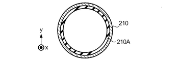
セル210は、内部空間を有する筒形状を有する。図1に示す例では、セル210は、円筒形状を有している。セル210の内部空間には、媒体の一例としてアルカリ金属ガスの一つであるセシウムガスが封入されている。
The
光ポンピングビーム照射装置230は、セル210に対して光ポンピングビーム230Aを照射する。具体的には、光ポンピングビーム照射装置230は、セル210の内部空間に封入されている媒体の光ポンピングに適した波長の円偏光を、光ポンピングビーム230Aとしてx軸方向(セル210の中心軸方向)からセル210へ照射して、セル210の内部空間を通過させる。これにより、セル210の内部空間に封入されている媒体の原子が励起され、電子スピンの向きが揃えられる。
The optical pumping
プローブ光照射装置220は、セル210に対してプローブ光220Aを照射する。具体的には、プローブ光照射装置220は、セル210の内部空間に封入されている媒体の原子の電子スピンの向きが揃えられた状態で、直線偏光を、プローブ光220Aとしてy軸方向(x軸方向と直交する方向)からセル210へ照射して、セル210の内部空間を通過させる。セル210の内部空間を通過したプローブ光220Aは、測定対象の測定位置での磁場の強度に応じて、偏光面が回転される。
The probe
検出装置240は、セル210から出射されたプローブ光220Aから、測定対象の測定位置における磁場の強度を検出する。たとえば、検出装置240は、偏光板によって、セル210から出射されたプローブ光220Aから特定の回転角度の偏光を透過する。そして、検出装置240は、フォトダイオードによって、偏光板を透過した偏光の強度を検出する。さらに、検出装置240は、検出した偏光の強度および回転角度に基づいて、セル210から出射されたプローブ光220Aの偏光回転角を算出する。そのうえ、検出装置240は、検出された偏光回転角に基づいて、測定対象の測定位置における磁場の強度を算出する。
The
本実施形態の磁場計測システム10は、原子励起層形成装置100をさらに備える。原子励起層形成装置100は、セル210に対して、原子励起層形成用ビーム100Aを照射して、セル210の壁部(セル210の壁部のうちのx軸方向に延伸する壁部)の内部空間側の表面(以下、「内壁面」という)に沿って、セル210の壁部の内部空間に原子励起層形成用ビーム100Aを通過させることにより、セル210の内壁面に、セル210の内部空間に封入されている媒体の原子を励起する原子励起層を形成する。具体的には、原子励起層形成装置100は、光ポンピングビーム230Aの波長と同一の波長の原子励起層形成用ビーム100Aをx軸方向からセル210の内部空間の端面へ照射して、セル210の内壁面に沿って、セル210の内部空間に原子励起層形成用ビーム100Aを通過させる。これにより、原子励起層形成装置100は、セル210の内壁面を覆う原子励起層であって、セル210に封入されている媒体の原子を励起する原子励起層を、セル210の内壁面における原子励起層形成用ビーム100Aの進行方向の全域に亘って均一に形成する。
The magnetic
原子励起層形成装置100は、セル210の内部空間の端面において、セル210の内部空間の端面を包含する面形状となる原子励起層形成用ビーム100Aを、セル210の内部空間の端面に対して照射することで、セル210の内壁面において、セル210の壁部の周方向の全域に亘って均一な原子励起層を形成する。たとえば、原子励起層形成装置100は、セル210の内部空間の端面において、セル210の内部空間の端面の形状と同一の面形状となる原子励起層形成用ビーム100Aを、セル210の内部空間の端面に対して照射する。図1に示す例では、セル210の内部空間の端面は円形状を有しているので、原子励起層形成装置100は、セル210の内部空間の端面において円形状となる原子励起層形成用ビーム100Aを、セル210の内部空間の端面に対して照射する。このようにして、原子励起層形成装置100は、セル210の内壁面の全域に亘って、均一かつ経年変化の少ない原子励起層を効率的に形成する。
In the atomic excitation
セル210の内壁面が原子励起層で覆われることで、セル210の壁部へ衝突した媒体の原子は、セル210の壁部の手前にある原子励起層で励起され、強制的に原子スピンが復帰される。原子励起層形成装置100は、セル210の内壁面に対して、不均一かつ経年変化の多い物理的なコーティングを施さずに、均一かつ経年変化の少ない原子励起層を形成するため、媒体の原子の原子スピンの緩和を抑制する効果を、均一かつ長期間継続して得ることができる。
By covering the inner wall surface of the
図2は、原子励起層が形成された状態のセル210の壁部の断面を示す。図2では、原子励起層が形成された状態のセル210の壁部を、原子励起層形成用ビーム100Aの進行方向であるx軸方向から見たときの断面を示す。原子励起層形成装置100は、セル210の内部空間の端面において、セル210の内壁面の周方向の全域に亘って、原子励起層形成用ビーム100Aを照射する。これにより、図2に示すように、セル210の内壁面には、セル210の内壁面の周方向の全域に亘って、セル210の内壁面を覆う原子励起層210Aが形成される。
FIG. 2 shows a cross section of the wall of the
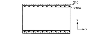
図3は、原子励起層が形成された状態のセル210の壁部の断面を示す。図3では、原子励起層が形成された状態のセル210壁部を、原子励起層形成用ビーム100Aの進行方向と直交する方向から見たときの断面を示す。原子励起層形成装置100は、セル210の内壁面に沿ってセル210の内部空間を通過する条件を満たす原子励起層形成用ビーム100Aを、セル210の内部空間の端面に対してx軸方向から照射する。たとえば、原子励起層形成装置100は、下記条件(1)および(2)を満たす原子励起層形成用ビーム100Aを、セル210の内部空間の端面に対してx軸方向から照射する。(1)セル210の内部空間の端面(断面)と同一の面形状を有する。(2)セル210の内部空間の軸方向と進行方向が平行である。
FIG. 3 shows a cross section of the wall portion of the
原子励起層形成装置100から照射された原子励起層形成用ビーム100Aは、セル210の内壁面に沿って、セル210の内部空間をx軸方向に通過する。これにより、図3に示すように、セル210の内壁面には、x軸方向(原子励起層形成用ビーム100Aの進行方向)の全域に亘って、セル210の内壁面を覆う原子励起層210Aが形成される。
The atomic excitation
<第2実施例>
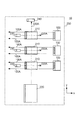
図4は、第2実施例に係る磁場計測システム10の構成を示す。図4に示す磁場計測システム10は、角筒形状のセル210が、プローブ光220Aの照射方向(y軸方向)に複数設けられており、複数のセル210のそれぞれに対して、光ポンピングビーム照射装置230と、原子励起層形成装置100とが設けられている点で、図1に示した磁場計測システム10と異なる。複数の原子励起層形成装置100のそれぞれは、第1実施例で説明した原子励起層形成装置100と同様に動作する。すなわち、複数の原子励起層形成装置100のそれぞれは、対応するセル210に原子励起層形成用ビーム100Aを照射することで、対応するセル210の内壁面に、原子励起層を形成する。
<Second embodiment>
FIG. 4 shows a configuration of the magnetic
第2実施例に係る磁場計測システム10によれば、複数のセル210のそれぞれに対して、セル210の内壁面において、セル210の内壁面の周方向の全域、および原子励起層形成用ビーム100Aの進行方向の全域に亘って均一な原子励起層を形成することができる。したがって、複数のセル210のそれぞれに対して、セルの内部空間に封入された媒体の原子の原子スピンの緩和を抑制する効果を、セル210の内壁面の周方向の全域、原子励起層形成用ビーム100Aの進行方向の全域に亘って得ることができる。また、複数のセル210のそれぞれに対して、経年変化の多い物理的なコーティングを施さずに、経年変化の少ない原子励起層を形成する。このため、複数のセル210のそれぞれに対して、原子励起層形成用ビーム100Aを照射し続けることで、媒体の原子の原子スピンの緩和を抑制する効果を、長期間継続して得ることができる。
According to the magnetic
なお、第2実施例に係る磁場計測システム10においては、セル210が1軸(y軸)方向に複数設けられているが、セル210が2軸方向に複数設けられてもよい。たとえば、複数のセル210が、x軸方向から見て格子状に並べて設けられてもよい。これらの場合も、複数のセル210の位置に対応して、複数の原子励起層形成装置100、および複数の光ポンピングビーム照射装置230を設け、複数のセル210のそれぞれに対して、第1実施例で説明した原子励起層形成装置100が照射する原子励起層形成用ビーム100Aと同条件の原子励起層形成用ビーム100Aを照射することで、複数のセル210のそれぞれの内壁面に、原子励起層を形成することができる。
In the magnetic
<第3実施例>
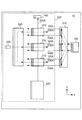
図5は、第3実施例に係る磁場計測システム10の構成を示す。図5に示す磁場計測システム10は、複数の原子励起層形成装置100の代わりに、一の原子励起層形成装置100と、光スプリッター510とを備える点で、図4に示した磁場計測システム10と異なる。光スプリッター510は、原子励起層形成装置100から出力された原子励起層形成用ビーム100Aを、複数の原子励起層形成用ビーム100Aに分岐する。具体的には、光スプリッター510は、原子励起層形成装置100の位置に対応して設けられた入射口から入射された原子励起層形成用ビーム100Aを、セル210の数分の原子励起層形成用ビーム100Aに分岐する。複数の原子励起層形成用ビーム100Aのそれぞれは、対応するセル210の位置に対応して設けられた出射口から出射され、対応するセル210に対して照射される。
<Third embodiment>
FIG. 5 shows a configuration of the magnetic
光スプリッター510は、複数のセル210のそれぞれに対して、第1実施例で説明した原子励起層形成装置100と同様に、セル210の内壁面に沿ってセル210の内部空間を通過する条件を満たす原子励起層形成用ビーム100Aを、セル210の内部空間の端面に対してx軸方向から照射する。すなわち、光スプリッター510は、複数のセル210のそれぞれに対して、第1実施例で説明した原子励起層形成装置100が照射する原子励起層形成用ビーム100Aと同条件の原子励起層形成用ビーム100Aを照射することで、複数のセル210のそれぞれの内壁面に、原子励起層を形成する。
The
第3実施例に係る磁場計測システム10によれば、複数のセル210のそれぞれに対して、セル210の内壁面において、セル210の内壁面の周方向の全域、および原子励起層形成用ビーム100Aの進行方向の全域に亘って均一な原子励起層を形成することができる。したがって、複数のセル210のそれぞれに対して、セルの内部空間に封入された媒体の原子の原子スピンの緩和を抑制する効果を、セル210の内壁面の周方向の全域、原子励起層形成用ビーム100Aの進行方向の全域に亘って得ることができる。また、複数のセル210のそれぞれに対して、経年変化の多い物理的なコーティングを施さずに、経年変化の少ない原子励起層を形成する。このため、複数のセル210のそれぞれに対して、原子励起層形成用ビーム100Aを照射し続けることで、媒体の原子の原子スピンの緩和を抑制する効果を、長期間継続して得ることができる。
According to the magnetic
特に、第3実施例に係る磁場計測システム10によれば、一の原子励起層形成装置100から出力された原子励起層形成用ビーム100Aを複数の原子励起層形成用ビーム100Aに分岐して、複数のセル210に照射するので、複数のセル210に照射される原子励起層形成用ビーム100Aのプロファイルのばらつきを容易に抑えることができる。また、複数のセル210に照射される原子励起層形成用ビーム100Aのプロファイルを変更する場合、原子励起層形成装置100から出力される原子励起層形成用ビーム100Aのプロファイルを変更すればよいため、複数のセル210に照射される原子励起層形成用ビーム100Aのプロファイルを容易に変更することができる。
In particular, according to the magnetic
図5に示す磁場計測システム10は、複数の光ポンピングビーム照射装置230の代わりに、一の光ポンピングビーム照射装置230と、光スプリッター520とを備える点でも、図4に示した磁場計測システム10と異なる。光スプリッター520は、光ポンピングビーム照射装置230から出力された光ポンピングビーム230Aを、複数の光ポンピングビーム230Aに分岐する。具体的には、光スプリッター520は、光ポンピングビーム照射装置230の位置に対応して設けられた入射口から入射された光ポンピングビーム230Aを、セル210の数分の光ポンピングビーム230Aに分岐する。複数の光ポンピングビーム230Aのそれぞれは、対応するセル210の位置に対応して設けられた出射口から出射され、対応するセル210に対して照射される。
The magnetic
第3実施例に係る磁場計測システム10によれば、一の光ポンピングビーム照射装置230から出力された光ポンピングビーム230Aを複数の光ポンピングビーム230Aに分岐して、複数のセル210に照射するので、複数のセル210に照射される光ポンピングビーム230Aのプロファイルのばらつきを容易に抑えることができる。また、複数のセル210に照射される光ポンピングビーム230Aのプロファイルを変更する場合、光ポンピングビーム照射装置230から出力される光ポンピングビーム230Aのプロファイルを変更すればよいため、複数のセル210に照射される光ポンピングビーム230Aのプロファイルを容易に変更することができる。
According to the magnetic
なお、第3実施例に係る磁場計測システム10においては、セル210が1軸(y軸)方向に複数設けられているが、セル210が2軸方向に複数設けられてもよい。たとえば、複数のセル210が、x軸方向から見て格子状に並べて設けられてもよい。これらの場合も、複数のセル210の位置に対応して、複数の原子励起層形成用ビーム100Aを照射する光スプリッター510、および複数の複数の光ポンピングビーム230Aを照射する光スプリッター520を設け、複数のセル210のそれぞれに対して、第1実施例で説明した原子励起層形成装置100が照射する原子励起層形成用ビーム100Aと同条件の原子励起層形成用ビーム100Aを照射することで、複数のセル210のそれぞれの内壁面に、原子励起層を形成することができる。
In the magnetic
第3実施例に係る磁場計測システム10において、原子励起層形成装置100および光スプリッター510を複数備え、複数の原子励起層形成装置100および光スプリッター510によって、複数のセル210のそれぞれに対して、原子励起層形成用ビーム100Aを照射してもよい。また、光ポンピングビーム照射装置230および光スプリッター520を複数備え、複数の光ポンピングビーム照射装置230および光スプリッター520によって、複数のセル210のそれぞれに対して、光ポンピングビーム230Aを照射してもよい。
The magnetic
本実施形態の磁場計測システム10は、第1実施例−第3実施例で説明した構成に限らない。たとえば、原子励起層形成装置100と光ポンピングビーム照射装置230とは、図4に示すように、セル210を挟んで対向して設けられていてもよく、図1に示すように、セル210の一方の方向に設けられていてもよい。また、磁場計測システム10は、磁場を計測するシステムであれば、生体計測システムに限らず、これ以外のシステムにも用いてもよい。また、原子励起層形成装置100は、セル210に封入されている媒体の光ポンピングに適した波長の円偏光であれば、光ポンピングビーム230Aの波長と同一の波長の原子励起層形成用ビーム100Aをセル210へ照射してもよく、光ポンピングビーム230Aの波長と異なる波長の原子励起層形成用ビーム100Aをセル210へ照射してもよい。
The magnetic
また、原子励起層形成装置100は、原子励起層形成用ビーム100Aの幅を調整することで、原子励起層の幅を調整することができる調整機構を有してもよい。これにより、たとえば、ユーザーは、原子励起層の幅を、光ポンピングセンサー感度が最も高くなるように、容易に調整することができる。
Further, the atomic excitation
また、セル210は、円筒形状および角筒形状に限らず、セル210の内壁面に沿って、セル210の内部空間に原子励起層形成用ビーム100Aを通過させることができるものであれば、これ以外の形状を有してもよい。また、原子励起層形成装置100は、セル210の内部空間の端面の形状に合わせて原子励起層形成用ビーム100Aの面形状を調整することができる調整機構を有していてもよい。また、セル210に封入される媒体には、セシウムガスに限らず、これ以外の、カリウムガス、ルビジウムガスなどのアルカリ金属ガスを用いてもよい。また、セル210に封入される媒体には、アルカリ金属ガスに限らず、これ以外の、希ガスなどの媒体を用いてもよい。また、原子励起層形成装置100は、セル210に封入されている媒体に合わせて原子励起層形成用ビーム100Aの波長を調整することができる調整機構を有していてもよい。
In addition, the
10…磁場計測システム、100…原子励起層形成装置、100A…原子励起層形成用ビーム、200…光ポンピング磁力計、210…セル、210A…原子励起層、220…プローブ光照射装置、220A…プローブ光、230…光ポンピングビーム照射装置、230A…光ポンピングビーム、240…検出装置、510…光スプリッター、520…光スプリッター
DESCRIPTION OF
Claims (7)
ことを特徴とする原子励起層形成方法。 A cell having an internal space provided in a measuring apparatus using optical pumping is irradiated with an atomic excitation layer forming beam, and the internal space is then moved along the surface of the wall portion of the cell to the internal space. An atomic excitation layer for exciting atoms of a medium enclosed in the internal space is formed on a surface of the cell wall portion on the internal space side by passing an atomic excitation layer forming beam. A method for forming an atomic excitation layer.
ことを特徴とする請求項1に記載の原子励起層形成方法。 2. The atom according to claim 1, wherein the end surface of the internal space is irradiated with the beam for forming an atomic excitation layer having a surface shape including the end surface of the internal space at an end surface of the internal space. Excitation layer forming method.
ことを特徴とする請求項1または2に記載の原子励起層形成方法。 The optical pumping beam irradiation apparatus provided in the measurement apparatus irradiates the cell with the beam for forming an atomic excitation layer having the same wavelength as that of the optical pumping beam applied to the cell. A method for forming an atomic excitation layer as described in 1. above.
ことを特徴とする原子励起層形成装置。 A cell having an internal space provided in a measuring apparatus using optical pumping is irradiated with an atomic excitation layer forming beam, and the internal space is then moved along the surface of the wall portion of the cell to the internal space. An atomic excitation layer for exciting atoms of a medium enclosed in the internal space is formed on a surface of the cell wall portion on the internal space side by passing an atomic excitation layer forming beam. An atomic excitation layer forming apparatus.
前記測定装置が備える内部空間を有するセルに対して、原子励起層形成用ビームを照射して、前記セルの壁部の前記内部空間側の表面に沿って、前記内部空間に前記原子励起層形成用ビームを通過させることにより、前記セルの壁部の前記内部空間側の表面に、前記内部空間に封入されている媒体の原子を励起する原子励起層を形成する原子励起層形成装置と
を備えることを特徴とする磁場計測システム。 A measuring device using optical pumping;
Irradiating an atomic excitation layer forming beam to a cell having an internal space provided in the measurement apparatus, and forming the atomic excitation layer in the internal space along the surface of the cell wall on the internal space side And an atomic excitation layer forming device that forms an atomic excitation layer that excites atoms of the medium enclosed in the internal space on the surface of the wall of the cell on the internal space side by passing the beam for use. Magnetic field measurement system characterized by this.
複数の前記セルを有し、
当該磁場計測システムは、
前記複数のセルのそれぞれに対して、前記原子励起層形成装置が設けられている
ことを特徴とする請求項5に記載の磁場計測システム。 The measuring device is
Having a plurality of said cells;
The magnetic field measurement system
The magnetic field measurement system according to claim 5, wherein the atomic excitation layer forming device is provided for each of the plurality of cells.
複数の前記セルを有し、
当該磁場計測システムは、
前記原子励起層形成装置から出力された前記原子励起層形成用ビームを、複数の前記原子励起層形成用ビームに分岐し、前記複数のセルのそれぞれに対して、前記原子励起層形成用ビームを照射して、前記セルの壁部の前記内部空間側の表面に沿って、前記内部空間に前記原子励起層形成用ビームを通過させる光スプリッターをさらに備える
ことを特徴とする請求項5に記載の磁場計測システム。 The measuring device is
Having a plurality of said cells;
The magnetic field measurement system
The atomic excitation layer forming beam output from the atomic excitation layer forming apparatus is branched into a plurality of atomic excitation layer forming beams, and the atomic excitation layer forming beam is supplied to each of the plurality of cells. The optical splitter according to claim 5, further comprising an optical splitter that irradiates and passes the atomic excitation layer forming beam through the internal space along a surface of the wall portion of the cell on the internal space side. Magnetic field measurement system.
Priority Applications (1)
| Application Number | Priority Date | Filing Date | Title |
|---|---|---|---|
| JP2009261968A JP2011106950A (en) | 2009-11-17 | 2009-11-17 | Atom excitation layer forming method, atom excitation layer forming device, and magnetic field measuring system |
Applications Claiming Priority (1)
| Application Number | Priority Date | Filing Date | Title |
|---|---|---|---|
| JP2009261968A JP2011106950A (en) | 2009-11-17 | 2009-11-17 | Atom excitation layer forming method, atom excitation layer forming device, and magnetic field measuring system |
Publications (1)
| Publication Number | Publication Date |
|---|---|
| JP2011106950A true JP2011106950A (en) | 2011-06-02 |
Family
ID=44230597
Family Applications (1)
| Application Number | Title | Priority Date | Filing Date |
|---|---|---|---|
| JP2009261968A Pending JP2011106950A (en) | 2009-11-17 | 2009-11-17 | Atom excitation layer forming method, atom excitation layer forming device, and magnetic field measuring system |
Country Status (1)
| Country | Link |
|---|---|
| JP (1) | JP2011106950A (en) |
Cited By (2)
| Publication number | Priority date | Publication date | Assignee | Title |
|---|---|---|---|---|
| WO2013008500A1 (en) * | 2011-07-13 | 2013-01-17 | 住友重機械工業株式会社 | Magnetoencephalography meter and neuromagnetism measuring method |
| CN103941199A (en) * | 2013-01-21 | 2014-07-23 | 精工爱普生株式会社 | Magnetic field measurement apparatus |
-
2009
- 2009-11-17 JP JP2009261968A patent/JP2011106950A/en active Pending
Cited By (3)
| Publication number | Priority date | Publication date | Assignee | Title |
|---|---|---|---|---|
| WO2013008500A1 (en) * | 2011-07-13 | 2013-01-17 | 住友重機械工業株式会社 | Magnetoencephalography meter and neuromagnetism measuring method |
| US9113803B2 (en) | 2011-07-13 | 2015-08-25 | Sumitomo Heavy Industries, Ltd. | Magnetoencephalography meter for measuring neuromagnetism |
| CN103941199A (en) * | 2013-01-21 | 2014-07-23 | 精工爱普生株式会社 | Magnetic field measurement apparatus |
Similar Documents
| Publication | Publication Date | Title |
|---|---|---|
| JP2017026402A (en) | Optical pumping magnetometer and magnetic sensing method | |
| JP6391370B2 (en) | Optical pumping magnetometer and magnetic sensing method | |
| Zhu et al. | Phonon spectroscopy with sub-meV resolution by femtosecond x-ray diffuse scattering | |
| von Korff Schmising et al. | Generating circularly polarized radiation in the extreme ultraviolet spectral range at the free-electron laser FLASH | |
| WO2012120732A1 (en) | Optically pumped magnetometer, magnetoencephalography meter, and mri device | |
| JP2017026405A (en) | Optical pumping magnetometer and magnetic sensing method | |
| Wang et al. | Complete polarization analysis of an APPLE II undulator using a soft X-ray polarimeter | |
| Vaudolon et al. | Photon counting technique applied to time-resolved laser-induced fluorescence measurements on a stabilized discharge | |
| JP2017190956A (en) | Magnetic measuring device and magnetic measuring method | |
| Eder et al. | Focusing of a neutral helium beam with a photon-sieve structure | |
| Bromberg et al. | Control of coherent backscattering by breaking optical reciprocity | |
| Hino et al. | Current status of BL06 beam line for VIN ROSE at J-PARC/MLF | |
| JP6678180B2 (en) | Radiation sensor device | |
| JP5914903B2 (en) | Magneto-optical effect measuring device | |
| JP2011106950A (en) | Atom excitation layer forming method, atom excitation layer forming device, and magnetic field measuring system | |
| US9766190B2 (en) | Method, system and apparatus for measuring comparatively thick materials | |
| CN109478428B (en) | Non-perturbative measurements of low and zero-point magnetic fields in high-temperature plasmas | |
| Curcio et al. | Single-shot non-intercepting profile monitor of plasma-accelerated electron beams with nanometric resolution | |
| JP2011137687A (en) | Magnetic measuring apparatus | |
| NL2015805A (en) | An Undulator | |
| KR101562854B1 (en) | SOLENOID COIL DEVICE AND IN-SITU He-3 NEUTRON SPIN POLARIZATION SYSTEM HAVING A SOLENOID COIL DEVICE | |
| CN103616649A (en) | Magnetic field sensor sensitivity tuning method based on fiber bragg grating laser | |
| JP2011106951A (en) | Electric field layer forming method, electric field layer forming device, and magnetic field measuring system | |
| CA2807120C (en) | Three-dimensional optical resonance device, polarized laser oscillation method, and polarized laser oscillation system | |
| JP6116053B2 (en) | Spin wave induction and initial phase control system and method, spin wave induction and propagation control system and method |