JP2011050007A5 - - Google Patents
Download PDFInfo
- Publication number
- JP2011050007A5 JP2011050007A5 JP2009198869A JP2009198869A JP2011050007A5 JP 2011050007 A5 JP2011050007 A5 JP 2011050007A5 JP 2009198869 A JP2009198869 A JP 2009198869A JP 2009198869 A JP2009198869 A JP 2009198869A JP 2011050007 A5 JP2011050007 A5 JP 2011050007A5
- Authority
- JP
- Japan
- Prior art keywords
- current
- current source
- circuit
- transistor
- stop
- Prior art date
- Legal status (The legal status is an assumption and is not a legal conclusion. Google has not performed a legal analysis and makes no representation as to the accuracy of the status listed.)
- Granted
Links
Images
Description
また、本実施形態のDA変換器は、上記基準電流を発生する基準電流発生回路を有しており、基準電流発生回路において基準電流の発生を停止することなく、電流源の動作を制御する。これにより、DA変換を必要としない期間が短い場合であっても、電流源の動作を停止させることができる。すなわち、基準電流発生回路として、基準電圧に応じた基準電流を発生させるフィードバックループを有する基準電流発生回路を用いた場合、基準電流発生回路の動作を停止すると、その後、動作を再開させるまでに時間がかかる。しかし、基準電流発生回路において基準電流の発生を停止することなく、電流源の動作を制御することにより、電流源の動作を迅速に再開させることができる。 The DA converter of this embodiment has a reference current generation circuit that generates the reference current, and controls the operation of the current source without stopping the generation of the reference current in the reference current generation circuit. Thereby, even when the period during which DA conversion is not required is short, the operation of the current source can be stopped. That is, when a reference current generation circuit having a feedback loop that generates a reference current corresponding to a reference voltage is used as the reference current generation circuit, when the operation of the reference current generation circuit is stopped, it takes time until the operation is restarted thereafter. It takes. However, the operation of the current source can be quickly restarted by controlling the operation of the current source without stopping the generation of the reference current in the reference current generating circuit.
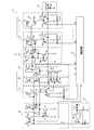
また、第2電流源部32は、電流源52と、第1電流源部31a〜31hの電流源51a〜51hの電流値を2段階(第1電流値と第2電流値)に切り替える切替回路62とを有している。電流源52は、NMOSトランジスタT41,T42がカスコード接続されて構成される。また、切替回路62は、ドレインが電源Vddに接続されたNMOSトランジスタT44と、ドレインがPMOSトランジスタT45を介して電源に接続されたNMOSトランジスタT43とを有している。切替回路62においては、NMOSトランジスタT44をオフ状態としたときに電流源51の電流値が第1電流値となり、NMOSトランジスタT44をオン状態としたときに電流源51の電流値が第2電流値となる。
The second
第3電流源部33には、電流源53の動作を停止するために、停止制御線S3にそのゲートが接続されたトランジスタT53を有している。このトランジスタT53は、電流源53と切替回路63との間に設けられる。そして、このトランジスタT53は、停止制御線S3により制御部50から制御され、電流源53から切替回路63への電流の供給と遮断を切り替える。すなわち、トランジスタT53は、電流源53の動作停止を行うスイッチとして機能する。このように、制御部50は、停止制御線S3に出力する制御信号を制御することで、電流源53の動作を停止することができる。
The third
(その他の回路構成)
電流伝達回路部20は、第3電流源部33の動作停止に伴う基準電流Irへの影響を抑制するために設けられる。
(Other circuit configuration)
また、第2電流伝達回路部34は、第2電流源部32の動作停止に伴う基準電流Irへの影響を抑制するために設けられる。
The second
また、図3(b)に示すように、切替回路62を構成する2つのNMOSトランジスタT43,T44の動作を同時に両方停止するために、NOR回路72を設けるようにしてもよい。この場合、切替回路62を構成する2つのNMOSトランジスタT43,T44が電流源52を停止するスイッチとして機能する。
Further, as shown in FIG. 3B, a NOR circuit 72 may be provided in order to simultaneously stop both the operations of the two NMOS transistors T43 and T44 constituting the
Priority Applications (3)
| Application Number | Priority Date | Filing Date | Title |
|---|---|---|---|
| JP2009198869A JP5418073B2 (en) | 2009-08-28 | 2009-08-28 | DA converter and solid-state imaging device |
| US12/845,224 US8587707B2 (en) | 2009-08-28 | 2010-07-28 | DA converter and solid-state imaging device that provides reduced power consumption |
| CN201010261283.7A CN102006077B (en) | 2009-08-28 | 2010-08-23 | DA converter and solid-state imaging device |
Applications Claiming Priority (1)
| Application Number | Priority Date | Filing Date | Title |
|---|---|---|---|
| JP2009198869A JP5418073B2 (en) | 2009-08-28 | 2009-08-28 | DA converter and solid-state imaging device |
Publications (3)
| Publication Number | Publication Date |
|---|---|
| JP2011050007A JP2011050007A (en) | 2011-03-10 |
| JP2011050007A5 true JP2011050007A5 (en) | 2012-10-04 |
| JP5418073B2 JP5418073B2 (en) | 2014-02-19 |
Family
ID=43624366
Family Applications (1)
| Application Number | Title | Priority Date | Filing Date |
|---|---|---|---|
| JP2009198869A Expired - Fee Related JP5418073B2 (en) | 2009-08-28 | 2009-08-28 | DA converter and solid-state imaging device |
Country Status (3)
| Country | Link |
|---|---|
| US (1) | US8587707B2 (en) |
| JP (1) | JP5418073B2 (en) |
| CN (1) | CN102006077B (en) |
Families Citing this family (21)
| Publication number | Priority date | Publication date | Assignee | Title |
|---|---|---|---|---|
| CN103688466B (en) * | 2011-07-20 | 2016-10-19 | 飞思卡尔半导体公司 | The method of at least one characteristic in IC apparatus and dynamically amendment digital to analog converter module |
| CN103427838B (en) * | 2012-05-25 | 2017-04-12 | 联发科技(新加坡)私人有限公司 | Switch driving circuit and digital-to-analog converter applying the same |
| US8599055B1 (en) * | 2012-07-24 | 2013-12-03 | Kathrein-Werke Kg | Digital-to-analog converter |
| US9258503B2 (en) * | 2012-12-06 | 2016-02-09 | Panasonic Intellectual Property Management Co., Ltd. | A/D converter, image sensor, and digital camera |
| JP2014165396A (en) * | 2013-02-26 | 2014-09-08 | Sony Corp | Solid imaging device and electronic apparatus |
| US9357150B2 (en) * | 2013-12-03 | 2016-05-31 | Capso Vision Inc. | Image sensor with integrated power conservation control |
| CN103873785B (en) * | 2014-03-26 | 2017-08-11 | 中国科学院光电技术研究所 | Low-noise charge coupled device front-end analog video signal preprocessing device |
| CN105988501B (en) * | 2015-02-27 | 2018-02-16 | 中芯国际集成电路制造(上海)有限公司 | A kind of current source and the biasing circuit for DAC |
| WO2017014070A1 (en) * | 2015-07-22 | 2017-01-26 | ソニーセミコンダクタソリューションズ株式会社 | Imaging element and electronic device |
| KR102386471B1 (en) * | 2015-10-28 | 2022-04-15 | 에스케이하이닉스 주식회사 | Ramp voltage generator, image sensing device with the ramp voltage generator and method of driving the image sensing device |
| CN108259804B (en) * | 2016-12-29 | 2021-06-29 | 扬智科技股份有限公司 | Video output system and related video signal compensation method |
| CN108471312A (en) * | 2017-02-23 | 2018-08-31 | 华邦电子股份有限公司 | Digital-to-analog converter |
| US10862501B1 (en) * | 2018-04-17 | 2020-12-08 | Ali Tasdighi Far | Compact high-speed multi-channel current-mode data-converters for artificial neural networks |
| US10804925B1 (en) * | 2018-04-17 | 2020-10-13 | Ali Tasdighi Far | Tiny factorized data-converters for artificial intelligence signal processing |
| JP7316673B2 (en) * | 2018-10-19 | 2023-07-28 | パナソニックIpマネジメント株式会社 | Imaging device |
| CN112217571B (en) * | 2019-07-09 | 2022-02-22 | 博通集成电路(上海)股份有限公司 | CMOS single-tube infrared transceiver |
| US10915298B1 (en) * | 2019-10-08 | 2021-02-09 | Ali Tasdighi Far | Current mode multiply-accumulate for compute in memory binarized neural networks |
| US11424755B2 (en) * | 2019-10-11 | 2022-08-23 | Regents Of The University Of Minnesota | System and method for a super-resolution digital-to-analog converter based on redundant sensing |
| US11539371B1 (en) * | 2021-09-27 | 2022-12-27 | Qualcomm Incorporated | Digital-to-analog converter (DAC) calibration using error DACs |
| KR20240110621A (en) * | 2021-12-13 | 2024-07-15 | 기가조트 테크널러지 인코포레이티드 | Low row noise ramp generator |
| CN116800068B (en) * | 2023-08-18 | 2024-01-02 | 北京紫光芯能科技有限公司 | Circuit unit for power supply switching, topology circuit and power supply system |
Family Cites Families (27)
| Publication number | Priority date | Publication date | Assignee | Title |
|---|---|---|---|---|
| JPH02288616A (en) * | 1989-04-28 | 1990-11-28 | Hitachi Ltd | Self-calibration type d/a converter and self-calibration type a/d converter using the d/a converter |
| JP2794786B2 (en) * | 1989-05-26 | 1998-09-10 | セイコーエプソン株式会社 | Digital-analog conversion circuit |
| JPH05206860A (en) * | 1992-01-24 | 1993-08-13 | Matsushita Electric Ind Co Ltd | Current addition type digital/analog conversion circuit |
| US5293166A (en) * | 1992-03-31 | 1994-03-08 | Vlsi Technology, Inc. | Digital-to-analog converter and bias compensator therefor |
| JP3085803B2 (en) * | 1992-11-26 | 2000-09-11 | 株式会社東芝 | Differential current source circuit |
| JPH06177766A (en) * | 1992-12-04 | 1994-06-24 | Toshiba Corp | D/a conversion circuit |
| US5592167A (en) * | 1994-10-19 | 1997-01-07 | Exar Corporation | Analog-digital converter using current controlled voltage reference |
| JP3062035B2 (en) * | 1995-03-31 | 2000-07-10 | インターナショナル・ビジネス・マシーンズ・コーポレ−ション | D / A converter |
| JP2872074B2 (en) * | 1995-04-21 | 1999-03-17 | 日本電気アイシーマイコンシステム株式会社 | Digital-to-analog converter |
| US5801653A (en) * | 1996-10-10 | 1998-09-01 | United Microelectronics Corporation | Current cell of a digital-to-analog converter |
| JPH10256914A (en) * | 1997-03-11 | 1998-09-25 | Toshiba Corp | D/a converter |
| JP3832943B2 (en) * | 1997-10-15 | 2006-10-11 | 沖電気工業株式会社 | Constant current source circuit and digital / analog conversion circuit using the same |
| JPH11175322A (en) * | 1997-12-17 | 1999-07-02 | Sony Corp | Information processor, information processing method and provision medium |
| JPH11261420A (en) | 1998-03-13 | 1999-09-24 | Matsushita Electric Ind Co Ltd | Digital/analog converter |
| JP4384356B2 (en) * | 1998-07-20 | 2009-12-16 | コーニンクレッカ フィリップス エレクトロニクス エヌ ヴィ | Flexible substrate |
| US6072415A (en) * | 1998-10-29 | 2000-06-06 | Neomagic Corp. | Multi-mode 8/9-bit DAC with variable input-precision and output range for VGA and NTSC outputs |
| KR100572313B1 (en) * | 1999-03-25 | 2006-04-19 | 삼성전자주식회사 | Digital-to-analog converter |
| JP2001136068A (en) * | 1999-11-08 | 2001-05-18 | Matsushita Electric Ind Co Ltd | Current summing type digital/analog converter |
| US6590516B2 (en) * | 2001-05-30 | 2003-07-08 | Matsushita Electric Industrial Co., Ltd. | Current steering type D/A converter |
| JP2003051747A (en) * | 2001-05-30 | 2003-02-21 | Matsushita Electric Ind Co Ltd | Current summing digital/analog converter |
| US6741195B1 (en) * | 2002-12-11 | 2004-05-25 | Micron Technology, Inc. | Low glitch current steering digital to analog converter and method |
| JP2005109962A (en) * | 2003-09-30 | 2005-04-21 | Seiko Epson Corp | D / A conversion apparatus and D / A conversion method |
| JP4470700B2 (en) | 2004-02-23 | 2010-06-02 | ソニー株式会社 | AD conversion method, AD converter, semiconductor device for detecting physical quantity distribution, and electronic apparatus |
| JP4107269B2 (en) * | 2004-02-23 | 2008-06-25 | ソニー株式会社 | Solid-state imaging device |
| US7156486B2 (en) * | 2004-02-23 | 2007-01-02 | Sony Corporation | Liquid ejection head, liquid ejection apparatus, and manufacturing method of the liquid ejection head |
| JP2005286552A (en) * | 2004-03-29 | 2005-10-13 | Ricoh Co Ltd | D/a converter |
| JP4682750B2 (en) * | 2005-08-22 | 2011-05-11 | ソニー株式会社 | DA converter |
-
2009
- 2009-08-28 JP JP2009198869A patent/JP5418073B2/en not_active Expired - Fee Related
-
2010
- 2010-07-28 US US12/845,224 patent/US8587707B2/en active Active
- 2010-08-23 CN CN201010261283.7A patent/CN102006077B/en not_active Expired - Fee Related
Similar Documents
| Publication | Publication Date | Title |
|---|---|---|
| JP2011050007A5 (en) | ||
| JP2014180213A5 (en) | ||
| JP2008178196A5 (en) | ||
| JP2011152023A5 (en) | ||
| JP5845112B2 (en) | Switch circuit | |
| TW201117556A (en) | Apparatus and method providing an interface between a first voltage domain and a second voltage domain | |
| JP2015153074A (en) | semiconductor device | |
| JP2015035652A (en) | Level shifter | |
| JP2011070761A5 (en) | ||
| WO2015003541A1 (en) | Power supply switching circuit and switching method between external power supply and battery power supply | |
| JP2016025801A (en) | Power-supply circuit | |
| JP2015122738A5 (en) | ||
| US8350611B1 (en) | Bandgap circuit and start circuit thereof | |
| TW201525295A (en) | Fan motor braking apparatus and method of controlling the same | |
| US20140139163A1 (en) | Fan control circuit | |
| CN104753404B (en) | Fan motor brake device and control method thereof | |
| JP2013250523A5 (en) | ||
| JP6349097B2 (en) | Input signal amplifier | |
| JP6543133B2 (en) | POWER SUPPLY DEVICE AND ITS CONTROL METHOD | |
| US9692415B2 (en) | Semiconductor device having low power consumption | |
| JP2010273186A5 (en) | ||
| JP2014049281A (en) | Switching method and device | |
| JP2016167807A5 (en) | ||
| JP2020047193A5 (en) | ||
| JP2006099507A5 (en) |