JP2011041109A - Transmission system, and transmission method - Google Patents
Transmission system, and transmission method Download PDFInfo
- Publication number
- JP2011041109A JP2011041109A JP2009188188A JP2009188188A JP2011041109A JP 2011041109 A JP2011041109 A JP 2011041109A JP 2009188188 A JP2009188188 A JP 2009188188A JP 2009188188 A JP2009188188 A JP 2009188188A JP 2011041109 A JP2011041109 A JP 2011041109A
- Authority
- JP
- Japan
- Prior art keywords
- transmission
- power supply
- operating frequency
- supply voltage
- macro
- Prior art date
- Legal status (The legal status is an assumption and is not a legal conclusion. Google has not performed a legal analysis and makes no representation as to the accuracy of the status listed.)
- Pending
Links
Images


Classifications
-
- H—ELECTRICITY
- H04—ELECTRIC COMMUNICATION TECHNIQUE
- H04B—TRANSMISSION
- H04B3/00—Line transmission systems
Abstract
Description
本発明はデータの伝送装置、伝送システム、伝送方法に関するものである。 The present invention relates to a data transmission apparatus, a transmission system, and a transmission method.
半導体集積回路の高性能化、動作周波数の向上に伴い、消費電力は年々増大する傾向にある。特に近年のデータ伝送速度の向上に伴い、大規模集積回路(LSI)全体におけるI/OやSERDES回路等のインタフェース(I/F)回路の電力比率が高くなってきており、I/F回路の低消費電力化が求められている。半導体集積回路の動作時の消費電力を主に決めている充放電による電力消費は、ほぼ電源電圧の2乗に比例する。従って、電源電圧を引き下げることは低消費電力化のために最も有効な手段であると言える。また、高速に動作するI/O回路や、SERDES回路等では、CML(Current Mode Logic)や、インピーダンスマッチング用の受端抵抗等が必須であり、これら定常的に電流を流す回路に対しても、電源電圧を引き下げることは消費電力低減のために効果的な手段である。 As the performance of semiconductor integrated circuits increases and the operating frequency increases, power consumption tends to increase year by year. In particular, with the recent increase in data transmission speed, the power ratio of interface (I / F) circuits such as I / O and SERDES circuits in the entire large scale integrated circuit (LSI) has increased. Low power consumption is required. The power consumption due to charging / discharging which mainly determines the power consumption during operation of the semiconductor integrated circuit is substantially proportional to the square of the power supply voltage. Therefore, it can be said that reducing the power supply voltage is the most effective means for reducing power consumption. Also, in I / O circuits and SERDES circuits that operate at high speed, CML (Current Mode Logic), receiving resistance for impedance matching, etc. are essential. Reducing the power supply voltage is an effective means for reducing power consumption.
一方、数Gpbsオーダーの高速I/Fでは伝送線路の伝送損失の増大や、シンボル間干渉(ISI:Inter Symbol Interference)の影響が顕著になり、正確なデータ伝送の障害となっている。高速I/Fではこの問題を解決するためにプリエンファシス技術やイコライザ技術等を用いて対応している。プリエンファシス技術は、予めISIの影響を考慮し、出力波形の0レベル及び1レベルの振幅を調整する技術であり、伝送線路通過後の波形をISIの影響をキャンセルした波形に近づけることが可能である。プリエンファシスのパラメータとしては、エンファシスの強弱を決定するエンファシス強度、エンファシスパターンを決定するTAP設定があり、最適な設定を行わなければ、ISIの影響を増大してしまうこともあり、伝送経路に合わせた高精度な設定が必要である。イコライザ技術は伝送線路通過後の伝送損失による波形振幅の減少を考慮して、入力波形に対し受信側のアンプにて高周波成分を増幅する技術である。イコライザ技術のパラメータとしてはイコライザ強度(増幅率の調整)があり、増幅しすぎても受信信号のS/N比(信号対雑音比)が低下し、増幅が足りないと伝送損失による波形減少を補うことができないため、伝送経路に合わせた高精度な設定が必要である。 On the other hand, in a high-speed I / F on the order of several Gpbs, an increase in transmission loss of a transmission line and the influence of inter-symbol interference (ISI) are remarkable, which is an obstacle to accurate data transmission. In order to solve this problem, the high-speed I / F uses a pre-emphasis technique, an equalizer technique, or the like. The pre-emphasis technology is a technology for adjusting the amplitudes of the 0 and 1 levels of the output waveform in consideration of the effect of ISI in advance, and the waveform after passing through the transmission line can be brought close to a waveform that cancels the effect of ISI. is there. Pre-emphasis parameters include emphasis strength that determines the strength of emphasis, and TAP settings that determine emphasis pattern. If the optimum setting is not performed, the effect of ISI may increase, and it may be adjusted to the transmission path. Highly accurate settings are required. The equalizer technique is a technique for amplifying a high frequency component with an amplifier on the receiving side with respect to an input waveform in consideration of a decrease in waveform amplitude due to transmission loss after passing through the transmission line. The equalizer technology parameter is equalizer strength (adjustment of amplification factor). Even if the signal is amplified too much, the S / N ratio (signal-to-noise ratio) of the received signal decreases. If the amplification is insufficient, the waveform decreases due to transmission loss. Since it cannot be compensated for, it is necessary to set with high accuracy according to the transmission path.
エンファシス制御やイコライザ強度のパラメータはLSI内の配線長差や、LSI間を結ぶ伝送路長の差、製造ばらつきによる差等による減衰特性の差に対しても高精度に調整が必要であり、実際の各伝送路毎に最適なパラメータ設定が必要である。このため、完成したシステム上で伝送特性評価を行いながら最適なパラメータを設定するトレーニングにより、エンファシス強度やTAP設定などを行うエンファシス制御や、イコライザ強度といったパラメータの設定値を決定する必要がある。 The parameters of emphasis control and equalizer strength need to be adjusted with high accuracy even for differences in attenuation characteristics due to differences in wiring length within LSI, differences in transmission path length between LSIs, differences due to manufacturing variations, etc. It is necessary to set optimum parameters for each transmission path. For this reason, it is necessary to determine setting values of parameters such as emphasis control for performing emphasis intensity and TAP setting and equalizer intensity by training for setting optimum parameters while evaluating transmission characteristics on a completed system.
I/F回路に対する電源電圧の最適化は様々な形態にて行われており、特許文献1にはTr/Tfをモニタし電源電圧を最適化するI/Fが示されている。また、特許文献2には複数の電源電圧仕様のI/Fを備え切り換えて使用することにより、電源電圧を最適化する回路が示されている。
Optimization of the power supply voltage for the I / F circuit is performed in various forms, and
消費電力を低減するには、動作環境に応じて高速I/Fの電源電圧を最適化するのが有効である。例えばある高速I/Fマクロについて、アプリケーションAに対しては、動作周波数帯10GHz、すなわち最大10GHzで動作している場合でも、別のアプリケーションBでは、動作周波数帯1GHz、すなわち最大1GHzでしか動作しない場合、アプリケーションBについては、電源電圧を引き下げることで、消費電力の低減が可能である。 In order to reduce power consumption, it is effective to optimize the power supply voltage of the high-speed I / F according to the operating environment. For example, for a certain high-speed I / F macro, even if the application A is operating at an operating frequency band of 10 GHz, that is, a maximum of 10 GHz, another application B operates only at an operating frequency band of 1 GHz, that is, a maximum of 1 GHz. In this case, the power consumption of the application B can be reduced by lowering the power supply voltage.
しかし、実際に高速I/Fに対して電源電圧の引き下げを行う場合、高速I/Fの持つパラメータを最適化するために多くの時間を要するという問題がある。高速I/Fはエンファシス強度、イコライザ強度、オフセット、送端抵抗値、電流源電圧値等のパラメータを有し、これらを高精度に最適化する必要がある。これらのパラメータは電源電圧の変動に対して最適値も変化する為、電源電圧を引き下げる場合には、電源電圧に合わせて各パラメータの最適化を行わなければならない。このため、電源電圧を引き下げた後で、各パラメータの最適化を実現するために、再調整や、再トレーニングが必要となる。特にエンファシス強度、イコライザ強度、オフセット等のトレーニングには、BER(Bit Error Rate)評価やEYEパターン評価による伝送性能の判定が必要であり、例えば10^5パターンの信号に対する評価をパラメータの組合せの全てに対して行う必要があるため、膨大な時間が必要となってしまう。 However, when the power supply voltage is actually lowered for the high-speed I / F, there is a problem that it takes a lot of time to optimize the parameters of the high-speed I / F. The high-speed I / F has parameters such as an emphasis intensity, an equalizer intensity, an offset, a transmission end resistance value, and a current source voltage value, and these need to be optimized with high accuracy. Since these parameters also change their optimum values with respect to fluctuations in the power supply voltage, when the power supply voltage is lowered, each parameter must be optimized in accordance with the power supply voltage. For this reason, after the power supply voltage is lowered, readjustment and retraining are necessary to optimize each parameter. Especially for training of emphasis strength, equalizer strength, offset, etc., it is necessary to judge transmission performance by BER (Bit Error Rate) evaluation and EYE pattern evaluation. Enormous amount of time is required.
本願において開示される発明のうち、代表的なものの概要を簡単に説明する。
送信機として働くI/Fと受信機として働くI/Fの、動作環境毎の最適な電源電圧および各種パラメータをテーブルとして格納しておき、動作環境の変動に応じて、テーブルを参照し、電源電圧および各種パラメータの最適化を行うことで上述の課題を解決する。これにより、動作環境の変動時に、短時間での最適化を行うことができる。
Among the inventions disclosed in the present application, outlines of typical ones will be briefly described.
The optimum power supply voltage and various parameters for each operating environment of the I / F functioning as a transmitter and the I / F functioning as a receiver are stored as a table, and the power supply is referenced by referring to the table according to the fluctuation of the operating environment. The above-described problems are solved by optimizing the voltage and various parameters. Thereby, it is possible to perform optimization in a short time when the operating environment changes.
本願によって開示される発明のうち、代表的なものによって得られる効果を簡単に説明すれば、以下の通りである。 The effects obtained by the representative ones of the inventions disclosed by the present application will be briefly described as follows.
I/Fの電源電圧を動作環境に応じて引き下げ、低消費電力化を実現することができる。また、I/Fの電源電圧を動作環境に応じて引き下げた際に、各パラメータを短時間にて最適化することが可能である。短時間でのパラメータの最適化を可能とすることで、装置動作中における動的な最適化も行うことができる。すなわち、I/Fの各種パラメータを最適に保ちながら、低消費電力化を実現することができる。 The power supply voltage of the I / F can be lowered according to the operating environment to achieve low power consumption. Further, when the I / F power supply voltage is lowered according to the operating environment, each parameter can be optimized in a short time. By enabling parameter optimization in a short time, dynamic optimization during operation of the apparatus can also be performed. That is, low power consumption can be realized while keeping various parameters of the I / F optimal.
以下、本発明を実施例に基づいて詳細に説明する。 Hereinafter, the present invention will be described in detail based on examples.
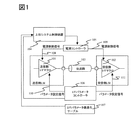
図1は高速I/Fを含んだ伝送システムの構成を示す図である。本実施例では、動作周波数帯に応じて送信機と受信機の電源電圧および各種パラメータを最適化するシステムを示す。本実施例の伝送システムは、送信側LSIの内部にある送信機となる送信側I/Fマクロ101と、受信側LSIの内部にある受信機となる受信側I/Fマクロ102と、送信側I/Fマクロ101と受信側I/Fマクロ102とを接続する伝送路103とを備える。送信側I/Fマクロ101は複数の動作周波数帯を有する。受信側マクロ102も、送信側マクロ101と対応する複数の動作周波数帯を有する。さらに、本実施例の伝送システムは、上位システム制御装置104と、電源コントローラ105と、I/Fパラメータコントローラ106と、I/Fパラメータ最適化テーブル107とを有する。
FIG. 1 is a diagram showing a configuration of a transmission system including a high-speed I / F. In this embodiment, a system for optimizing the power supply voltage and various parameters of the transmitter and the receiver according to the operating frequency band is shown. The transmission system according to the present embodiment includes a transmission side I / F macro 101 serving as a transmitter inside the transmission side LSI, a reception side I /
電源コントローラ105はシステム上のI/Fに供給する電源電圧を制御する回路であり、例えばDC−DCコンバータを備えたような制御回路である。I/Fパラメータコントローラ106は送信側I/Fマクロ101、受信側I/Fマクロ102に対して各IFパラメータの設定を行う。I/Fパラメータ最適化テーブル107は、例えば、RAMやフラッシュメモリ、レジスタファイル、ハードディスク等の記憶装置に格納されている。I/Fパラメータ最適化テーブル107には、伝送システムの動作周波数帯毎の、予め求められている、送信側I/Fマクロ101と受信側I/Fマクロ102の電源電圧、エンファシス強度、イコライザ強度が含まれている。
The
本実施例の伝送システムの動作を説明するために、例として、送信側LSIと受信側LSIも含めたシステム全体が扱うアプリケーションがアプリケーションAからアプリケーションBに変化したことにより、動作周波数が最大で5GHzから最大で0.5GHzに変化した場合、すなわち、すなわち動作周波数帯を5GHzから0.5GHzに下げた場合に、電源電圧およびI/Fの各種パラメータを最適化する場合の動作の説明を行う。 In order to explain the operation of the transmission system of the present embodiment, as an example, the operating frequency of the entire system including the transmission side LSI and the reception side LSI is changed from application A to application B, so that the maximum operating frequency is 5 GHz. The operation when the power supply voltage and various parameters of the I / F are optimized will be described when the frequency changes from 0.5 GHz to 0.5 GHz, that is, when the operating frequency band is lowered from 5 GHz to 0.5 GHz.
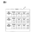
上位システム制御装置104は、送信側LSIと受信側LSIも含めたシステム全体の稼動状態をモニタし、送信側I/Fマクロ101と受信側I/Fマクロ102の動作周波数帯、すなわち伝送システムの動作周波数帯を決定する。この例では、上位システム制御装置104が、アプリケーションAからアプリケーションBに切り替わった事をモニタ、検出し、送信側I/Fマクロ101と受信側I/Fマクロ102の動作周波数帯を5GHzから0.5GHzへ下げることを決定する。上位システム制御装置104は、さらに、決定した動作周波数帯に基づいて、送信側I/Fマクロ101と受信側I/Fマクロ102の、最適な電源電圧値と各種I/Fパラメータの設定情報をI/Fパラメータ最適化テーブル107から取得する。例えば、I/Fパラメータ最適化テーブル107には、図2のI/Fパラメータ最適化テーブル201に示すデータが前もって格納されている。このテーブルを「動作周波数帯0.5GHz」をキーワードにして検索すると、「電源電圧」、「エンファシス強度」、「イコライザ強度」の各パラメータを取得することができる。消費電力を下げることを目的としているため、上位システム制御装置104は、I/Fパラメータ最適化テーブル107から取得可能なパラメータの中で最も電源電圧の低い条件を選ぶ。本実施例では、「電源電圧0.6(V)」、「エンファシス強度1」、「イコライザ強度1」というパラメータが取得される。本実施例では、送信側I/Fマクロ101の設定パラメータとしてはエンファシス強度を、受信側I/Fマクロ102の設定パラメータとしてはイコライザ強度をテーブル化する例を示したが、エンファシス強度、イコライザ強度以外に、出力振幅制御値、送端抵抗制御値などを予めテーブル化して取得することもできる。
The host
上位システム制御装置104は、I/Fパラメータ最適化テーブル107から取得した電源電圧の設定パラメータを電源コントローラ105へ、各I/FのパラメータをI/Fパラメータコントローラ106に出力する。電源コントローラ105は、上位システム制御装置104から取得したパラメータに基づいて、送信側I/Fマクロ101に対して電源制御信号108を、受信側I/Fマクロ102に対して電源制御信号109をそれぞれ送信し、送信側I/Fマクロ101と受信側I/Fマクロ102の電源電圧の設定を行う。これにより、送信側I/Fマクロ101、受信側I/Fマクロ102の電源電圧の最適化、すなわち低電力化を行うことができる。なお、本実施例では、送信側I/Fマクロ101、受信側I/Fマクロ102とに同じ電源電圧値を設定しているが、互いに異なる電源電圧値が最適値の場合もある。互いに異なる電源電圧値がそれぞれの最適値の場合には、それぞれの最適な電源電圧値をI/Fパラメータ最適化テーブル107に格納しておき、送信側I/Fマクロ101と受信側I/Fマクロ102とにそれぞれの最適な電源電圧の設定を行う。I/Fパラメータコントローラ106は、上位システム制御装置104から取得したパラメータに基づいて、送信側I/Fマクロ101に対してパラメータ設定信号110を、受信側I/Fマクロ102に対してパラメータ設定信号111を送信し、各I/Fパラメータの設定を行う。本実施例では、送信側I/Fマクロ101と受信側I/Fマクロ102とに電源電圧0.6Vが設定され、「エンファシス強度1」が送信側I/Fマクロ101に対して設定され、「イコライザ強度1」が受信側I/Fマクロ102に対して設定される。これにより、低電力のために最適化されている電源電圧が瞬時に得られ、低電力のために最適化されている電源電圧において最適化されているI/Fパラメータが、電源電圧を変化させる前後の間で再調整や再トレーニングを行うことなく、短時間に設定される。従って、アプリケーションが変わり、動作周波数帯が変化する際に、動的に伝送システムの低電力化を行うことができる。
The host
図3に本実施例の伝送システムにおいて、動作環境が変化し、動作周波数帯の切替が行われた際にI/Fパラメータの最適化を行う処理のフローチャートを示す。ステップ301で動作環境が変化した場合はステップ302へ進む。本実施例の説明において動作環境が変化した場合とは、上述のように、システムが処理するアプリケーションがアプリケーションAからアプリケーションBに変化した場合である。動作環境が変化したかどうかの判断は、上位システム制御装置104が行う。動作環境の変化を検出しない限りはステップ301で待機し、動作環境の変化を待つ。従って、動作環境の変化が無ければ、I/Fに設定されている条件を保持した状態でデータの伝送が行われる。動作環境の変化があって、ステップ302に進むと、上位システム制御装置104が、変化後の動作環境に合った動作周波数帯を決定する。動作周波数帯が決定されると、ステップ303にて上位システム制御装置104がI/Fパラメータ最適化テーブル107を参照し、電源電圧設定情報とI/Fパラメータ設定情報を取得し、ステップ304へ進む。ステップ304では、I/Fパラメータ最適化テーブル107から取得したパラメータ値の、送信側I/Fマクロ101と受信側I/Fマクロ102への設定が行われる。上位システム制御装置104が取得した電源電圧設定情報とI/Fパラメータ設定情報は、電源コントローラ105とI/Fパラメータコントローラ106を介して、送信側I/Fマクロ101と受信側I/Fマクロ102の電源電圧とI/Fパラメータとして設定され、動作周波数帯の切り替えが終了する。切り替えの終了後、ステップ301へ戻る。以上のように、動作環境の変化に応じて、動的に送信側I/Fマクロ101と受信側I/Fマクロ102の電源電圧とI/Fパラメータの切り替えが行われる。
FIG. 3 shows a flowchart of processing for optimizing the I / F parameter when the operating environment changes and the operating frequency band is switched in the transmission system of this embodiment. If the operating environment has changed in
実施例1のI/Fパラメータ最適化テーブル107の作成は、外部装置を実施例1の伝送システムに接続して行うことができるが、伝送システムに組み込まれているテスト装置で行うことも可能である。実施例2では、伝送システムにトレーニングモードを実行するテスト装置を組み込んだ場合の実施例を示す。 The creation of the I / F parameter optimization table 107 of the first embodiment can be performed by connecting an external device to the transmission system of the first embodiment, but can also be performed by a test apparatus incorporated in the transmission system. is there. In the second embodiment, an embodiment in which a test apparatus that executes a training mode is incorporated in the transmission system will be described.
図4に、トレーニングモードを実行するテスト装置を組み込んだ場合の、送信側I/Fの構成を示す。送信側I/F401は入力端子に入力されたLSI内部信号を、出力端子から後述の受信用I/Fへと接続されている伝送路408に向けて出力するものである。送信側I/F401はドライバ回路402、スイッチング回路404、トレーニング信号発生器405を備える。
FIG. 4 shows a configuration of the transmission-side I / F when a test apparatus that executes the training mode is incorporated. The transmission-side I /
ドライバ回路402はI/Fパラメータを持つ出力回路であり、例えばCMOSタイプやCMLタイプの回路により構成される。I/Fパラメータ設定情報403はI/Fパラメータコントローラ407から送信される信号である。I/Fパラメータ設定情報403はドライバ回路402のI/Fパラメータを制御する信号であり、例えばエンファシス強度制御や出力振幅制御、送端抵抗制御等の制御信号である。スイッチング回路404は通常モードと後述するトレーニングモードを切り換える回路であり、上位システム制御装置から送信される通常モード/トレーニングモード切替制御信号406により制御される。トレーニング信号発生器405はトレーニング時に使用する信号を発生する回路であり、例えばPRBS(Pseudo Random Binary Sequence)等の疑似ランダムパターンを発生する信号発生器である。なお、図4ではトレーニング信号発生器405を送信側I/F401の内部に有する構成例を示しているが、送信側I/F401の外部、またはシステムの外部に実装することも可能である。
The driver circuit 402 is an output circuit having an I / F parameter, and is configured by, for example, a CMOS type or CML type circuit. The I / F
図5に受信側I/Fの詳細を示す。受信側I/F501の通常動作は、送信側I/F401に接続されている伝送路408を介し入力端子に受信した信号を、出力端子からLSI内部に向けて伝送するものである。受信側I/F501はレシーバ回路502、スイッチング回路504、ループバックパス505、ループバック用ドライバ506を備える。レシーバ回路502はI/Fパラメータをもつ入力回路であり、例えばCMOSタイプやCMLタイプの回路により構成される。I/Fパラメータ設定情報503はレシーバ回路502のI/Fパラメータを制御する信号であり、例えばイコライザ強度制御やオフセット調整制御、受端抵抗制御等の制御信号である。スイッチング回路504は通常モードと後述するトレーニングモードを切り換える回路であり、上位システム制御装置からの通常モード/トレーニングモード切替制御信号508により制御される。ループバックパス505とループバック用ドライバ506はトレーニングモードにて使用する観測経路であり、レシーバ回路502の受信した信号をループバックモニタ端子510に出力する。
FIG. 5 shows details of the reception side I / F. The normal operation of the reception-side I / F 501 is to transmit a signal received at the input terminal via the
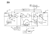
図6は図4、図5で示したI/Fを含んだシステムのトレーニングモードについて説明した図である。ここでのトレーニング対象は伝送路408で接続された送信側I/Fマクロ401と受信側I/Fマクロ502である。トレーニング時には各I/Fマクロをトレーニングモードに切り替える。
FIG. 6 is a diagram for explaining the training mode of the system including the I / F shown in FIGS. The training target here is the transmission side I /
各I/Fマクロをトレーニングモードに切り換えることで、トレーニング用信号の発生や、受信信号をモニタ信号に出力するループバックを行うことが可能となる。トレーニングモードへの切替は、上位システム制御装置からの通常モード/トレーニングモード切替制御信号607により行う。送信側I/Fマクロ401はトレーニングモードに切り換えた場合の形態であり、トレーニング信号発生器405から出力した信号を、スイッチング回路404を介し、ドライバ回路402から伝送路408を通じ受信側I/Fマクロ501に向けて送信する。受信側I/Fマクロ501はループバックモードに切り換えた場合の例である。レシーバ回路502にて受信した信号を、スイッチング回路504を介し、ループバックパス505を通じてループバック用ドライバ506から出力する。信号観測回路606は信号観測機能を有するものであり、例えばBER測定や、EYEマスクパタン判定等の機能を持つものである。
By switching each I / F macro to the training mode, it is possible to generate a training signal and perform a loopback that outputs a received signal to a monitor signal. Switching to the training mode is performed by a normal mode / training mode switching control signal 607 from the host system control device. The transmission side I /
信号観測回路606はドライバ回路402の出力信号613とループバック用ドライバ506からの出力信号614を比較し伝送性能に対する判定を行う。なお、入力端子617での出力信号の波形を観測することによりドライバ回路402より出力された波形について伝送路を通過した後の状態で観測することもできる。信号観測回路606による伝送性能の判定を必要に応じてI/Fパラメータの組合せを換えながら実行し、トレーニング結果、すなわち判定結果をI/Fパラメータ最適化テーブル616内へ格納する。なお信号観測回路606の実装については、システム内部、システム外部のどちらでも可能であり、システム外部に実装する場合はBERTやオシロスコープ等の測定装置を利用することも可能である。また、システム内に実装する場合は、I/Fマクロと共通のLSI上に実装することも可能である。
The
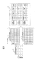
図7にエンファシス強度[7:0]、イコライザ強度[7:0]をパラメータに持つI/Fに対するトレーニングおよび、I/Fパラメータ最適化テーブルに格納されるデータの例を示す。この例では、トレーニングのパラメータとして動作周波数帯と電源電圧を選んでいる。動作環境パラメータ701は、電源電圧を0.6V、1.0V、1.2Vと、動作周波数帯を0.5GHz、2.5GHz、5.0GHzとした場合である。動作環境パラメータ701から決定する各A〜Iの条件に対して、エンファシス強度[7:0]、イコライザ強度[7:0]を総当りで切替え、BERを取得する。動作環境パラメータ701の条件で取得したBER結果の例をトレーニング結果702,703に示す。動作環境パラメータ701の全ての条件に対して取得したBER結果からI/Fパラメータ最適化データを取得し、I/Fパラメータ最適化テーブル704内に格納する。I/Fパラメータ最適化テーブルは、あるキーワードに対してI/Fパラメータを決定するものであり、図7に示すように動作周波数帯と電源電圧に対してI/Fパラメータを決定するものに限らず、様々なキーワードに対してI/Fパラメータを決定するテーブルも実現することができる。例えば、I/Fパラメータ最適化テーブル作成時に、電源電圧をパラメータとしたトレーニングを行い、同じ動作周波数帯であっても、より短距離の伝送経路では、電源電圧を引き下げることができる等、伝送路長に合わせた電源電圧の最適化を行うことが可能である。
FIG. 7 shows an example of training for an I / F having parameters of emphasis intensity [7: 0] and equalizer intensity [7: 0] and data stored in the I / F parameter optimization table. In this example, an operating frequency band and a power supply voltage are selected as training parameters. The operating
図8に図6に示す構成の、図7に示すトレーニング例における、トレーニングのフローチャートを示す。トレーニングを行う際にはまずステップ801にてI/Fをトレーニングモードに切り換える。トレーニングモードへの切り替えの信号は、上位システム制御装置から発せられる。ステップ802で動作環境パラメータの初期値を設定する。動作環境パラメータとは電源電圧や動作周波数帯等を決定するパラメータである。その他の動作環境パラメータとしては、温度や伝送路長等も挙げることができる。ステップ803ではI/Fパラメータを初期化する。ステップ802とステップ803で決定する動作環境パラメータとI/Fパラメータの初期値はトレーニングの初期状態であり、トレーニングの仕様に合わせて任意に変更することが可能である。ステップ804でトレーニング信号を発生する。このとき図6のトレーニング信号発生器405から出力された信号は、スイッチング回路404を介し、ドライバ回路402から伝送路408を通じ受信側I/Fマクロ501に向けて送信される。受信側I/Fマクロ501はレシーバ回路502にて受信した信号を、スイッチング回路504を介し、ループバックパス505と通じてループバック用ドライバ506から出力する。ステップ805でトレーニング結果の取得を行う。信号観測回路606は、伝送性能を観測し、判定する。例えば、ドライバ回路402の出力信号613とループバック用ドライバ506からの出力信号614を比較しBER評価を行い、判定を行う。ステップ806ではトレーニング結果をI/Fパラメータ最適化テーブルへ格納する。例えばトレーニング結果702のエンファシス強度1、イコライザ強度2の判定が決定した時点でI/Fパラメータ最適化テーブルへトレーニング結果を格納する。ステップ807で、必要なI/Fパラメータの組合せに対するトレーニングが完了したかを判定する。必要なI/Fパラメータの組合せはトレーニングの仕様、目的に応じて任意に決定するものである。図7の例では、必要なI/Fパラメータの組合せはエンファシス強度[7:0]パターン、イコライザ強度[7:0]パターンで64パターンの組合せとなる。必要なI/Fパラメータの組合せに対するトレーニングが完了していれば、ステップ809へ進む。必要なI/Fパラメータの組合せに対するトレーニングが完了していない場合は、ステップ808へ進み、新たにI/Fパラメータの組合せを設定し、ステップ805へ進む。ステップ809で必要な動作環境パラメータの組合せに対するトレーニングが完了したかを判定する。必要な動作環境パラメータの組合せはトレーニングの仕様、目的に応じて任意に決定するものである。図7の例では、必要な動作環境パラメータの組合せは電源電圧が0.6V、1.0V、1.2V、動作周波数帯がそれぞれの電源電圧に対して0.5GHz、2.5GHz、5.0GHzの計9パターンの組合せとなる。必要な動作環境パラメータの組合せが完了していない場合は、ステップ810へ進み新たに動作環境パラメータを設定し、ステップ803へ進む。必要な動作環境パラメータの組合せが完了していれば、トレーニングは完了となり、I/Fパラメータ最適化テーブルが完成する。以上のステップ801〜810によりトレーニングが完了する。これにより、予めI/Fの最適な電源電圧とI/Fパラメータのテーブルを得ることができる。
FIG. 8 shows a flowchart of training in the training example shown in FIG. 7 having the configuration shown in FIG. When performing the training, first, in
以上、本実施形態によって、本発明を詳細に説明したが、上記に限定されるものではなく、その要旨を逸脱しない範囲で変更が可能である。 As mentioned above, although this invention was demonstrated in detail by this embodiment, it is not limited above, It can change in the range which does not deviate from the summary.
本発明の伝送システムは、LSI間のデータ伝送などに用いて好適なものである。 The transmission system of the present invention is suitable for use in data transmission between LSIs.
101・・・送信側I/Fマクロ、102・・・受信側I/Fマクロ、103・・・伝送路、104・・・上位システム制御装置、105・・・電源コントローラ、106・・・I/Fパラメータコントローラ、107・・・I/Fパラメータ最適化テーブル、108・・・電流制御信号、109・・・電流制御信号、110・・・パラメータ設定信号、111・・・パラメータ設定信号、201・・・I/Fパラメータ最適化テーブル、301〜304・・・I/Fパラメータの最適化を行う処理のフローチャートの各ステップ、401・・・送信側I/Fマクロ、402・・・ドライバ回路、403・・・I/Fパラメータ設定情報、404・・・スイッチング回路、405・・・トレーニング信号発生器、406・・・通常モード/トレーニングモード切替制御信号、407・・・I/Fパラメータコントローラ、408・・・伝送路、501・・・受信側I/Fマクロ、502・・・レシーバ回路、503・・・I/Fパラメータ設定情報、606・・・信号観測回路、607・・・通常モード/トレーニングモード切替制御信号、613・・・ドライバ出力信号、614・・・ループバックパス用ドライバ出力信号、616・・・I/Fパラメータ最適化テーブル、701・・・動作環境パラメータ、702・・・トレーニング結果、703・・・トレーニング結果、704・・・I/Fパラメータ最適化テーブル、801〜810・・・I/Fパラメータを決定するトレーニングのフローチャートの各ステップ
DESCRIPTION OF SYMBOLS 101 ... Transmission side I / F macro, 102 ... Reception side I / F macro, 103 ... Transmission path, 104 ... Host system controller, 105 ... Power supply controller, 106 ... I / F parameter controller, 107 ... I / F parameter optimization table, 108 ... current control signal, 109 ... current control signal, 110 ... parameter setting signal, 111 ... parameter setting signal, 201 ... I / F parameter optimization table, 301 to 304 ... each step of the flowchart of the process for optimizing the I / F parameter, 401 ... transmission side I / F macro, 402 ...
Claims (10)
第2LSIと、
前記第1LSI内に設けられ、複数の動作周波数帯を有する送信側インタフェースマクロと、
前記第2LSI内に設けられ、前記複数の動作周波数帯で動作する受信側インタフェースマクロと、
前記送信側インタフェースマクロと前記受信側インタフェースマクロとを接続する伝送路と、
前記送信側インタフェースマクロと前記受信側インタフェースマクロの、前記複数の動作周波数帯毎の電源電圧と設定パラメータのテーブルとを有し、
前記複数の動作周波数帯の内から使用する動作周波数帯に応じて、前記送信側インタフェースマクロと前記受信側インタフェースマクロの電源電圧と設定パラメータとを、前記テーブルから選択することを特徴とする伝送システム。 A first LSI;
A second LSI;
A transmission-side interface macro provided in the first LSI and having a plurality of operating frequency bands;
A receiving-side interface macro provided in the second LSI and operating in the plurality of operating frequency bands;
A transmission line connecting the transmission side interface macro and the reception side interface macro;
A power supply voltage and a setting parameter table for each of the plurality of operating frequency bands of the transmission side interface macro and the reception side interface macro;
A transmission system, wherein a power supply voltage and a setting parameter of the transmission side interface macro and the reception side interface macro are selected from the table according to an operation frequency band used from the plurality of operation frequency bands. .
前記設定パラメータは、エンファシス強度を含むことを特徴とする伝送システム。 The transmission system according to claim 1, wherein
The transmission system, wherein the setting parameter includes an emphasis strength.
前記設定パラメータは、イコライザ強度を含むことを特徴とする伝送システム。 The transmission system according to claim 1, wherein
The transmission system, wherein the setting parameter includes an equalizer strength.
上位システム制御装置をさらに有し、
前記上位システム制御装置は、前記第1LSIと前記第2LSIとが処理するアプリケーションに応じて、前記複数の動作周波数帯の内から使用する動作周波数帯を選択することを特徴とする伝送システム。 The transmission system according to claim 1, wherein
It further has a host system control device,
The transmission system according to claim 1, wherein the host system control device selects an operating frequency band to be used from the plurality of operating frequency bands in accordance with an application processed by the first LSI and the second LSI.
前記複数の動作周波数帯で動作する受信機と、
前記送信機と前記受信機とを接続する伝送路と、
前記送信機と前記受信機の、前記複数の動作周波数帯毎の電源電圧と設定パラメータのテーブルとを有し、
前記複数の動作周波数帯の内から使用する動作周波数帯に応じて、前記送信機と前記受信機の電源電圧と設定パラメータとを、前記テーブルから選択することを特徴とする伝送システム。 A transmitter having a plurality of operating frequency bands;
A receiver operating in the plurality of operating frequency bands;
A transmission line connecting the transmitter and the receiver;
A power supply voltage and a setting parameter table for each of the plurality of operating frequency bands of the transmitter and the receiver;
The transmission system, wherein a power supply voltage and a setting parameter of the transmitter and the receiver are selected from the table according to an operating frequency band used from the plurality of operating frequency bands.
前記設定パラメータは、エンファシス強度を含むことを特徴とする伝送システム。 The transmission system according to claim 5, wherein
The transmission system, wherein the setting parameter includes an emphasis strength.
前記設定パラメータは、イコライザ強度を含むことを特徴とする伝送システム。 The transmission system according to claim 6,
The transmission system, wherein the setting parameter includes an equalizer strength.
前記複数の動作周波数帯で動作する受信機と、
前記送信機と前記受信機とを接続する伝送路と、
前記送信機と前記受信機の、前記複数の動作周波数帯毎の電源電圧と設定パラメータのテーブルとを有する伝送システムを準備し、
前記複数の動作周波数帯の内の一つを選択し、
前記選択した動作周波数帯に対応する電源電圧と設定パラメータとを前記テーブルから取得し、
前記取得した電源電圧と設定パラメータとを、前記送信機と前記受信機とに設定することを特徴とするデータの伝送方法。 A transmitter having a plurality of operating frequency bands;
A receiver operating in the plurality of operating frequency bands;
A transmission line connecting the transmitter and the receiver;
Preparing a transmission system having a power supply voltage and a setting parameter table for each of the plurality of operating frequency bands of the transmitter and the receiver;
Selecting one of the plurality of operating frequency bands;
A power supply voltage and a setting parameter corresponding to the selected operating frequency band are acquired from the table,
A data transmission method, wherein the acquired power supply voltage and setting parameters are set in the transmitter and the receiver.
前記設定パラメータは、エンファシス強度を含むことを特徴とするデータの伝送方法。 The data transmission method according to claim 8,
The data transmission method, wherein the setting parameter includes an emphasis strength.
前記設定パラメータは、イコライザ強度を含むことを特徴とするデータの伝送方法。 The data transmission method according to claim 8,
The data transmission method, wherein the setting parameter includes an equalizer strength.
Priority Applications (2)
| Application Number | Priority Date | Filing Date | Title |
|---|---|---|---|
| JP2009188188A JP2011041109A (en) | 2009-08-17 | 2009-08-17 | Transmission system, and transmission method |
| US12/834,777 US20110038426A1 (en) | 2009-08-17 | 2010-07-12 | Transmission system and transmission method |
Applications Claiming Priority (1)
| Application Number | Priority Date | Filing Date | Title |
|---|---|---|---|
| JP2009188188A JP2011041109A (en) | 2009-08-17 | 2009-08-17 | Transmission system, and transmission method |
Publications (2)
| Publication Number | Publication Date |
|---|---|
| JP2011041109A true JP2011041109A (en) | 2011-02-24 |
| JP2011041109A5 JP2011041109A5 (en) | 2012-04-26 |
Family
ID=43588582
Family Applications (1)
| Application Number | Title | Priority Date | Filing Date |
|---|---|---|---|
| JP2009188188A Pending JP2011041109A (en) | 2009-08-17 | 2009-08-17 | Transmission system, and transmission method |
Country Status (2)
| Country | Link |
|---|---|
| US (1) | US20110038426A1 (en) |
| JP (1) | JP2011041109A (en) |
Cited By (5)
| Publication number | Priority date | Publication date | Assignee | Title |
|---|---|---|---|---|
| JP2013201725A (en) * | 2012-03-26 | 2013-10-03 | Fujitsu Ltd | Transmission characteristic adjustment device, transmitter, and transmission characteristic adjustment method |
| JP2015177492A (en) * | 2014-03-18 | 2015-10-05 | 株式会社リコー | Communication device and communication system |
| US9509446B2 (en) | 2013-10-17 | 2016-11-29 | Nec Corporation | Signal transmission system, signal receiving device, signal sending device, signal receiving device control program, and signal transmission method |
| JP2018207444A (en) * | 2017-06-09 | 2018-12-27 | 富士通株式会社 | Information processing device, program, and information system |
| US10614896B2 (en) | 2018-06-12 | 2020-04-07 | Hitachi, Ltd. | Non-volatile memory device and interface configuration method |
Families Citing this family (2)
| Publication number | Priority date | Publication date | Assignee | Title |
|---|---|---|---|---|
| WO2012109857A1 (en) * | 2011-07-29 | 2012-08-23 | 华为技术有限公司 | Bandwidth adjustment method, bus controller and signal converter |
| US8933737B1 (en) * | 2013-06-28 | 2015-01-13 | Stmicroelectronics International N.V. | System and method for variable frequency clock generation |
Citations (4)
| Publication number | Priority date | Publication date | Assignee | Title |
|---|---|---|---|---|
| JP2006262088A (en) * | 2005-03-17 | 2006-09-28 | Seiko Epson Corp | Radio communication equipment |
| JP2007053648A (en) * | 2005-08-19 | 2007-03-01 | Fujitsu Ltd | Device having communication function, and method, system, and program for automatic adjustment of transmitter |
| WO2007108125A1 (en) * | 2006-03-23 | 2007-09-27 | Fujitsu Limited | Parameter control circuit |
| JP2008022392A (en) * | 2006-07-14 | 2008-01-31 | Hitachi Ltd | Serializer/deserializer type transfer device |
Family Cites Families (9)
| Publication number | Priority date | Publication date | Assignee | Title |
|---|---|---|---|---|
| US6278305B1 (en) * | 1998-02-09 | 2001-08-21 | Matsushita Electric Industrial, Ltd. | Semiconductor integrated circuit |
| JP2002344304A (en) * | 2001-05-15 | 2002-11-29 | Fujitsu Ltd | Differential amplifier circuit and semiconductor integrated circuit device |
| JP2005136572A (en) * | 2003-10-29 | 2005-05-26 | Renesas Technology Corp | Semiconductor integrated circuit for radio communication, semiconductor integrated circuit for data processing and portable terminal |
| JP2005337740A (en) * | 2004-05-24 | 2005-12-08 | Matsushita Electric Ind Co Ltd | High-speed interface circuit inspection module, object module for high-speed interface circuit inspection, and high-speed interface circuit inspection method |
| JP2006059910A (en) * | 2004-08-18 | 2006-03-02 | Fujitsu Ltd | Semiconductor device |
| JP4808247B2 (en) * | 2006-03-27 | 2011-11-02 | 富士通株式会社 | Peaking control circuit |
| JP4730840B2 (en) * | 2006-11-15 | 2011-07-20 | ルネサスエレクトロニクス株式会社 | Semiconductor integrated circuit for communication and radio communication terminal device using the same |
| JP2009232406A (en) * | 2008-03-25 | 2009-10-08 | Fujitsu Ltd | Clock interface, clock signal setting method, and communication equipment |
| JP5268412B2 (en) * | 2008-04-22 | 2013-08-21 | 株式会社日立製作所 | Output driver circuit device |
-
2009
- 2009-08-17 JP JP2009188188A patent/JP2011041109A/en active Pending
-
2010
- 2010-07-12 US US12/834,777 patent/US20110038426A1/en not_active Abandoned
Patent Citations (4)
| Publication number | Priority date | Publication date | Assignee | Title |
|---|---|---|---|---|
| JP2006262088A (en) * | 2005-03-17 | 2006-09-28 | Seiko Epson Corp | Radio communication equipment |
| JP2007053648A (en) * | 2005-08-19 | 2007-03-01 | Fujitsu Ltd | Device having communication function, and method, system, and program for automatic adjustment of transmitter |
| WO2007108125A1 (en) * | 2006-03-23 | 2007-09-27 | Fujitsu Limited | Parameter control circuit |
| JP2008022392A (en) * | 2006-07-14 | 2008-01-31 | Hitachi Ltd | Serializer/deserializer type transfer device |
Cited By (5)
| Publication number | Priority date | Publication date | Assignee | Title |
|---|---|---|---|---|
| JP2013201725A (en) * | 2012-03-26 | 2013-10-03 | Fujitsu Ltd | Transmission characteristic adjustment device, transmitter, and transmission characteristic adjustment method |
| US9509446B2 (en) | 2013-10-17 | 2016-11-29 | Nec Corporation | Signal transmission system, signal receiving device, signal sending device, signal receiving device control program, and signal transmission method |
| JP2015177492A (en) * | 2014-03-18 | 2015-10-05 | 株式会社リコー | Communication device and communication system |
| JP2018207444A (en) * | 2017-06-09 | 2018-12-27 | 富士通株式会社 | Information processing device, program, and information system |
| US10614896B2 (en) | 2018-06-12 | 2020-04-07 | Hitachi, Ltd. | Non-volatile memory device and interface configuration method |
Also Published As
| Publication number | Publication date |
|---|---|
| US20110038426A1 (en) | 2011-02-17 |
Similar Documents
| Publication | Publication Date | Title |
|---|---|---|
| JP2011041109A (en) | Transmission system, and transmission method | |
| US6980824B2 (en) | Method and system for optimizing transmission and reception power levels in a communication system | |
| JP5969605B2 (en) | Single-end configurable multimode driver | |
| JP4886435B2 (en) | Automatic adjustment circuit for differential signal amplitude | |
| JP5039988B2 (en) | Digital transmission circuit | |
| US8937975B1 (en) | Apparatus and method for providing pre-emphasis to a signal | |
| KR20060131883A (en) | System and method for automatically calibrating two-tap and multi-tap equalization for a communications link | |
| US20060226868A1 (en) | Semiconductor device capable of controlling OCD and ODT circuits and control method used by the semiconductor device | |
| US8290028B2 (en) | Input/output circuit | |
| KR20110003725A (en) | Transceiver for controlling the swing width of output voltage, method for controlling the swing width of output voltage | |
| JP2007274139A (en) | Automatic preemphasis adjusting method and data transmission system | |
| JP2017514393A (en) | SERDES voltage mode driver with skew correction | |
| JP5017903B2 (en) | Pre-emphasis adjustment method and method | |
| US20210075650A1 (en) | Bi-level adaptive equalizer | |
| JP2021027489A (en) | Data transmission device and control method thereof | |
| TWI724544B (en) | Communication receiving device and clock data recovery method | |
| KR101148596B1 (en) | Voltage-mode driver with capacitive coupling equalizer and pre-emphasis method in the voltage-mode drivers | |
| JPWO2009031404A1 (en) | Transmission circuit, transmitter, receiver, and test apparatus | |
| Xu et al. | Q-Learning-Based Voltage-Swing Tuning and Compensation for 2.5-D Memory-Logic Integration | |
| JP4048377B2 (en) | Equalizer device and method for adjusting equalizer circuit | |
| JPWO2020080125A1 (en) | Communication system, transmitter, and receiver | |
| US8195107B2 (en) | Signal transmission system and signal transmission method thereof | |
| JP2020039576A (en) | Semiconductor device | |
| CN112491429B (en) | Communication receiving device and clock data recovery method | |
| TWI466462B (en) | Gain adjustment device and gain adjustment method for wireless communication circuit |
Legal Events
| Date | Code | Title | Description |
|---|---|---|---|
| A521 | Request for written amendment filed |
Free format text: JAPANESE INTERMEDIATE CODE: A523 Effective date: 20120308 |
|
| A621 | Written request for application examination |
Free format text: JAPANESE INTERMEDIATE CODE: A621 Effective date: 20120308 |
|
| A977 | Report on retrieval |
Free format text: JAPANESE INTERMEDIATE CODE: A971007 Effective date: 20130509 |
|
| A131 | Notification of reasons for refusal |
Free format text: JAPANESE INTERMEDIATE CODE: A131 Effective date: 20130521 |
|
| A02 | Decision of refusal |
Free format text: JAPANESE INTERMEDIATE CODE: A02 Effective date: 20131001 |