JP2011030283A - Battery controller and battery pack - Google Patents
Battery controller and battery pack Download PDFInfo
- Publication number
- JP2011030283A JP2011030283A JP2009170054A JP2009170054A JP2011030283A JP 2011030283 A JP2011030283 A JP 2011030283A JP 2009170054 A JP2009170054 A JP 2009170054A JP 2009170054 A JP2009170054 A JP 2009170054A JP 2011030283 A JP2011030283 A JP 2011030283A
- Authority
- JP
- Japan
- Prior art keywords
- voltage
- turned
- transistor
- node
- fet
- Prior art date
- Legal status (The legal status is an assumption and is not a legal conclusion. Google has not performed a legal analysis and makes no representation as to the accuracy of the status listed.)
- Withdrawn
Links
Images


Classifications
-
- Y—GENERAL TAGGING OF NEW TECHNOLOGICAL DEVELOPMENTS; GENERAL TAGGING OF CROSS-SECTIONAL TECHNOLOGIES SPANNING OVER SEVERAL SECTIONS OF THE IPC; TECHNICAL SUBJECTS COVERED BY FORMER USPC CROSS-REFERENCE ART COLLECTIONS [XRACs] AND DIGESTS
- Y02—TECHNOLOGIES OR APPLICATIONS FOR MITIGATION OR ADAPTATION AGAINST CLIMATE CHANGE
- Y02E—REDUCTION OF GREENHOUSE GAS [GHG] EMISSIONS, RELATED TO ENERGY GENERATION, TRANSMISSION OR DISTRIBUTION
- Y02E60/00—Enabling technologies; Technologies with a potential or indirect contribution to GHG emissions mitigation
- Y02E60/10—Energy storage using batteries
Landscapes
- Charge And Discharge Circuits For Batteries Or The Like (AREA)
- Secondary Cells (AREA)
Abstract
Description
本発明は、電池制御装置および電池パックに関し、特に、リチウムイオン二次電池を監視する電池制御装置、ならびに、この電池制御装置とリチウムイオン二次電池を含んだ電池パックに適用して有効な技術に関する。 The present invention relates to a battery control device and a battery pack, and more particularly, to a battery control device that monitors a lithium ion secondary battery, and a technique that is effective when applied to a battery pack including the battery control device and a lithium ion secondary battery. About.
例えば、特許文献1には、充電保護用FETならびに放電保護用FETと、各FETを制御する制御ICとを備えた二次電池保護回路において、過充電時の制御方式が示されている。二次電池に対する過充電が制御ICによって検出されると、充電保護用FETがオフに駆動され、このFETに並列接続された順方向ダイオードを介する放電のみが可能となる。しかしながら、この状態で二次電池に負荷が接続されると、負荷の駆動電流が順方向ダイオードの電流に制限されてしまう。そこで、制御ICは、この順方向ダイオードに電流が流れた際に生じる順方向電圧を検出し、この検出を受けて充電保護用FETを再びオンに駆動する制御回路を備える。
For example,
例えば、携帯電話機を代表とする携帯用電子機器では、軽量、高容量、サイクル寿命の長さなどの理由から、殆どの場合にリチウムイオン二次電池が用いられている。しかしながら、リチウムイオン二次電池は、高容量のために過充電または外部接続端子間の短絡などの状態では、膨張、発熱、発火の危険性が高い。そのため危険状態を回避するため、リチウムイオン二次電池には、制御装置が装着される。制御装置では、主に二次電池における過充電電圧、過放電電圧、過放電電流、短絡電流、過充電電流等が監視ICによって検出され、これらの検出結果に応じて放電保護用FET(Field Effect Transistor)ならびに充電保護用FETの制御が行われる。 For example, in portable electronic devices typified by mobile phones, lithium ion secondary batteries are used in most cases for reasons such as light weight, high capacity, and long cycle life. However, since the lithium ion secondary battery has a high capacity, there is a high risk of expansion, heat generation, and ignition in a state such as overcharging or a short circuit between external connection terminals. Therefore, in order to avoid a dangerous state, a control device is attached to the lithium ion secondary battery. In the control device, an overcharge voltage, an overdischarge voltage, an overdischarge current, a short-circuit current, an overcharge current, etc. mainly in a secondary battery are detected by a monitoring IC, and a discharge protection FET (Field Effect) is detected according to these detection results. Transistor) and the charge protection FET are controlled.
ここで、監視ICは、過充電電圧を検出した際、充電保護用FETの充電電流パスを遮断する。この状態で、二次電池に対して負荷が接続された場合、図9に示すように、二次電池に対して、充電保護用FETのボディーダイオードを通る放電経路が形成される。図9は、本発明の前提として検討した電池パックにおいて、その過充電電圧検出後の状態を示す説明図である。図9に示すように、監視IC(MIC)は、二次電池BATに対する過充電電圧を検出すると、充電制御端子CHGを介して充電保護用FET(FET_C)をオフに制御する。この状態では、BAT→負荷LD→FET_CのボディーダイオードD1→放電保護用FET(FET_D)の放電経路DPHが形成される。 Here, the monitoring IC cuts off the charging current path of the charge protection FET when detecting the overcharge voltage. In this state, when a load is connected to the secondary battery, as shown in FIG. 9, a discharge path is formed through the body diode of the charge protection FET for the secondary battery. FIG. 9 is an explanatory diagram showing a state after detection of the overcharge voltage in the battery pack studied as a premise of the present invention. As shown in FIG. 9, when the monitoring IC (MIC) detects an overcharge voltage for the secondary battery BAT, the monitoring IC (MIC) controls the charge protection FET (FET_C) to be turned off via the charge control terminal CHG. In this state, a discharge path DPH of BAT → load LD → FET_C body diode D1 → discharge protection FET (FET_D) is formed.
一方、監視ICは、過放電電流や短絡電流の検出に際しては、設定値以上の放電電流が流れたことを検出して放電保護用FET(FET_D)の放電電流パスを遮断する。その具体的な方式として、監視ICは、通常状態(FET(FET_C,FET_D)が共にオン状態)を前提として、電流値検出端子IDTを介して、このFETに流れる電流を、そのオン抵抗の電圧降下で生じる電圧値として検知している。つまり、検出したい電流値は、FETのオン抵抗から計算した検出電圧値に置き換えて設定されている。 On the other hand, when detecting the overdischarge current or the short-circuit current, the monitoring IC detects that the discharge current exceeding the set value has flowed, and interrupts the discharge current path of the discharge protection FET (FET_D). As a specific method, the monitoring IC assumes a normal state (both FETs (FET_C, FET_D) are on), and converts the current flowing through the FET through the current value detection terminal IDT to the voltage of its on-resistance. It is detected as a voltage value caused by a drop. That is, the current value to be detected is set by replacing the detected voltage value calculated from the on-resistance of the FET.
ここで、例えば、図9に示したような状態で前述した過放電電流の検出を行ってしまうと、FET(FET_C,FET_D)が共にオン状態という前提が変わるため、検出される電圧値に対する流れた電流が変わってしまう。その為、一般的に、過充電電圧が検出され充電保護用FET(FET_C)が遮断された場合、過充電状態から回復するまでの間、過放電電流の検出機能は停止状態とされる。一方、短絡電流の検出機能は、通常、短絡電流を検出する設定値が比較的大きな値となることや、当該機能を停止させると短絡電流により電池パックが破壊される事態を招く恐れがあることなどから通常通り有効とされる。 Here, for example, if the above-described overdischarge current is detected in the state shown in FIG. 9, the premise that both the FETs (FET_C, FET_D) are in the on state changes. Current will change. Therefore, generally, when the overcharge voltage is detected and the charge protection FET (FET_C) is cut off, the overdischarge current detection function is stopped until the overcharge state is recovered. On the other hand, the short-circuit current detection function usually has a relatively large set value for detecting the short-circuit current, and if the function is stopped, the short-circuit current may cause the battery pack to be destroyed. It is effective as usual.
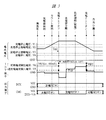
図10は、本発明の前提として検討した電池パックにおいて、その動作例を示すシーケンス図である。図10に示すシーケンスは、これまでに説明した動作を纏めたものである。図10に示すように、二次電池BATに充電器を接続した後、BATの電圧値が過充電に該当する充電停止電圧V1に到達すると、それが一定の期間(Tsp3)継続するのを確認して、充電保護用FET(FET_C)がオフに制御される。その状態で、充電器を分離すると、電流値検出端子IDTにおいて正方向の電圧が検出される。この正方向の電圧は、監視IC(MIC)がIDTを介して充電器が分離されたことを認識するためにIDTから微小な電流を流出し、この電流が順方向のボディーダイオードD1を流れることで生じる。 FIG. 10 is a sequence diagram showing an operation example of the battery pack studied as a premise of the present invention. The sequence shown in FIG. 10 summarizes the operations described so far. As shown in FIG. 10, after the charger is connected to the secondary battery BAT, when the BAT voltage value reaches the charge stop voltage V1 corresponding to overcharge, it is confirmed that it continues for a certain period (Tsp3). Then, the charge protection FET (FET_C) is controlled to be turned off. When the charger is separated in this state, a positive voltage is detected at the current value detection terminal IDT. This positive voltage causes a small current to flow out of the IDT so that the monitoring IC (MIC) recognizes that the charger has been separated via the IDT, and this current flows through the body diode D1 in the forward direction. It occurs in.
その後、二次電池BATに対して充電器に替わり負荷LDが接続されると、これに伴う放電電流によってIDTにおける正方向の電圧は更に上昇する。一方、BATでは、放電電流に伴い電池電圧が低下するため、電池電圧が充電停止復帰電圧V2まで低下した段階で充電保護用FET(FET_C)が再びオンに制御される。これによって、IDTの電圧は、負荷LDの動作電流に応じた正常な値まで低下する。このような動作において、前述したように、FET_Cがオフ状態(TA)となってから再びオン状態(TB)となるまでの間は、過放電電流の検出機能は停止状態とされる。 After that, when the load LD is connected to the secondary battery BAT instead of the charger, the positive voltage in the IDT further increases due to the discharge current associated therewith. On the other hand, in BAT, since the battery voltage decreases with the discharge current, the charge protection FET (FET_C) is turned on again when the battery voltage decreases to the charge stop recovery voltage V2. As a result, the IDT voltage drops to a normal value corresponding to the operating current of the load LD. In such an operation, as described above, the over-discharge current detection function is stopped until the FET_C is turned off (TA) and then turned on again (TB).
しかしながら、近年では、FET(FET_C,FET_D)による損失の低減、ならびに電池効率向上のため、そのオン抵抗は著しく低減されてきている。これによって、図10に示す、過放電電流を検出する際の過放電電流検出電圧V5、ならびに短絡電流を検出する際の短絡電流検出電圧V6は、低めに設定せざるを得ない状況にある。したがって、特に短絡電流検出電圧V6の設定が低い場合、図10のTA〜TBの間において、負荷LDの通常の動作電流によってもボディーダイオードD1の特性に伴い短絡電流の発生と判断され、放電保護用FET(FET_D)を遮断されてしまう状況が起こり得る。この場合、FET_D、FET_Cが共にオフ状態となり、負荷LDに対して動作電流を供給できず、実使用上の不具合が生じ得る。 However, in recent years, on-resistance has been remarkably reduced in order to reduce loss due to FETs (FET_C, FET_D) and improve battery efficiency. As a result, the overdischarge current detection voltage V5 when detecting the overdischarge current and the short circuit current detection voltage V6 when detecting the short circuit current shown in FIG. 10 must be set lower. Therefore, especially when the setting of the short-circuit current detection voltage V6 is low, it is determined that a short-circuit current is generated in accordance with the characteristics of the body diode D1 between TA and TB in FIG. A situation may occur in which the FET (FET_D) is blocked. In this case, both FET_D and FET_C are turned off, and an operating current cannot be supplied to the load LD, which may cause a problem in actual use.
また、本来ならば、図10のTA〜TBの間においても過放電電流を検出することが望ましいが、過放電電流検出電圧V5の設定が低くなると、場合によっては負荷LDを接続せずとも充電器を分離しただけで過放電電流の発生と判断され得る。この場合も同様に、FET_D、FET_Cが共にオフ状態となり、負荷LDに対して動作電流を供給できず、実使用上の不具合が生じ得る。 Further, originally, it is desirable to detect the overdischarge current also between TA and TB in FIG. 10, but if the setting of the overdischarge current detection voltage V5 becomes low, charging may be performed without connecting the load LD in some cases. It can be determined that the overdischarge current is generated only by separating the device. In this case as well, both FET_D and FET_C are turned off, and an operating current cannot be supplied to the load LD, which may cause a problem in actual use.
本発明は、このような問題を見出すことでなされたものであり、その目的の一つは、適切な安全性を確保することが可能な電池制御装置ならびにそれを含んだ電池パックを提供することにある。本発明の前記並びにその他の目的と新規な特徴は、本明細書の記述及び添付図面から明らかになるであろう。 The present invention has been made by finding such a problem, and one of its purposes is to provide a battery control device capable of ensuring appropriate safety and a battery pack including the same. It is in. The above and other objects and novel features of the present invention will be apparent from the description of this specification and the accompanying drawings.
本願において開示される発明のうち、代表的な実施の形態の概要を簡単に説明すれば、次のとおりである。 Of the inventions disclosed in the present application, the outline of a typical embodiment will be briefly described as follows.
本実施の形態による電池制御装置は、二次電池の充放電電流経路上の第1および第2ノード間に直列に挿入された充電保護用スイッチおよび放電保護用スイッチと、充電保護用スイッチに並列接続され、二次電池からの放電電流のみを流す第1ダイオードと、放電保護用スイッチに並列接続され、二次電池への充電電流のみを流す第2ダイオードと、二次電池の電圧および電流を監視し各スイッチを制御する監視ICとを備えている。監視ICは、充電保護用スイッチおよび放電保護用スイッチを共にオンに制御している際には、第1ノードと第2ノード間の電位差が第1A判定電圧を超え、それが一定期間継続した場合に短絡電流と判断して放電保護用スイッチをオフに制御する。一方、監視ICは、二次電池の過充電に伴い充電保護用スイッチをオフ、放電保護用スイッチをオンに制御している際には、第1ノードと第2ノード間の電位差が第1B判定電圧(>第1A判定電圧)を超え、それが一定期間継続した場合に短絡電流と判断して放電保護用スイッチをオフに制御する。 The battery control device according to the present embodiment is parallel to the charge protection switch and the charge protection switch inserted in series between the first and second nodes on the charge / discharge current path of the secondary battery, and the charge protection switch. A first diode that is connected and flows only the discharge current from the secondary battery, a second diode that is connected in parallel to the switch for discharge protection and flows only the charge current to the secondary battery, and the voltage and current of the secondary battery A monitoring IC that monitors and controls each switch. When the monitoring IC controls both the charge protection switch and the discharge protection switch to be on, the potential difference between the first node and the second node exceeds the first A determination voltage, and this continues for a certain period of time. The discharge protection switch is controlled to be turned off by determining that the current is a short-circuit current. On the other hand, when the monitoring IC controls the charge protection switch to be turned off and the discharge protection switch to be turned on due to overcharge of the secondary battery, the potential difference between the first node and the second node is determined to be 1B. When the voltage (> 1A determination voltage) is exceeded and continues for a certain period, it is determined as a short-circuit current and the switch for discharge protection is controlled to be turned off.
これによって、過充電が検出された状態で負荷が接続されたような場合でも、負荷に対して十分な動作電流を供給しつつ、短絡電流を適切に判定することが可能となり、二次電池の安全性を適切に確保することが可能となる。また、仮に過充電状態の有無に関わらず判定電圧を変えない場合には、充電保護用スイッチならびに放電保護用スイッチのオン抵抗が低減されるほど負荷の動作電流の確保が困難となるが、判定電圧を変えることで十分な動作電流を確保でき、結果的に、各スイッチのオン抵抗を低減でき、高効率な電池パックが実現可能となる。 As a result, even when a load is connected with overcharge detected, it is possible to appropriately determine the short-circuit current while supplying a sufficient operating current to the load. It becomes possible to ensure safety appropriately. Also, if the judgment voltage is not changed regardless of the presence or absence of an overcharged state, it becomes more difficult to secure the operating current of the load as the on-resistance of the charge protection switch and the discharge protection switch is reduced. By changing the voltage, a sufficient operating current can be secured, and as a result, the on-resistance of each switch can be reduced and a highly efficient battery pack can be realized.
本願において開示される発明のうち、代表的な実施の形態によって得られる効果を簡単に説明すると、二次電池の適切な安全確保が実現可能になる。 Of the inventions disclosed in this application, the effects obtained by the representative embodiments will be briefly described. As a result, it is possible to ensure appropriate safety of the secondary battery.
以下の実施の形態においては便宜上その必要があるときは、複数のセクションまたは実施の形態に分割して説明するが、特に明示した場合を除き、それらは互いに無関係なものではなく、一方は他方の一部または全部の変形例、詳細、補足説明等の関係にある。また、以下の実施の形態において、要素の数等(個数、数値、量、範囲等を含む)に言及する場合、特に明示した場合および原理的に明らかに特定の数に限定される場合等を除き、その特定の数に限定されるものではなく、特定の数以上でも以下でも良い。 In the following embodiment, when it is necessary for the sake of convenience, the description will be divided into a plurality of sections or embodiments. However, unless otherwise specified, they are not irrelevant, and one is the other. Some or all of the modifications, details, supplementary explanations, and the like are related. Further, in the following embodiments, when referring to the number of elements (including the number, numerical value, quantity, range, etc.), especially when clearly indicated and when clearly limited to a specific number in principle, etc. Except, it is not limited to the specific number, and may be more or less than the specific number.
さらに、以下の実施の形態において、その構成要素(要素ステップ等も含む)は、特に明示した場合および原理的に明らかに必須であると考えられる場合等を除き、必ずしも必須のものではないことは言うまでもない。同様に、以下の実施の形態において、構成要素等の形状、位置関係等に言及するときは、特に明示した場合および原理的に明らかにそうでないと考えられる場合等を除き、実質的にその形状等に近似または類似するもの等を含むものとする。このことは、上記数値および範囲についても同様である。 Further, in the following embodiments, the constituent elements (including element steps and the like) are not necessarily indispensable unless otherwise specified and apparently essential in principle. Needless to say. Similarly, in the following embodiments, when referring to the shapes, positional relationships, etc. of the components, etc., the shapes are substantially the same unless otherwise specified, or otherwise apparent in principle. And the like are included. The same applies to the above numerical values and ranges.
また、実施の形態の各機能ブロックを構成する回路素子は、特に制限されないが、公知のCMOS(相補型MOSトランジスタ)等の集積回路技術によって、単結晶シリコンのような半導体基板上に形成される。 The circuit elements constituting each functional block of the embodiment are not particularly limited, but are formed on a semiconductor substrate such as single crystal silicon by a known integrated circuit technology such as a CMOS (complementary MOS transistor). .
以下、本発明の実施の形態を図面に基づいて詳細に説明する。なお、実施の形態を説明するための全図において、同一の部材には原則として同一の符号を付し、その繰り返しの説明は省略する。 Hereinafter, embodiments of the present invention will be described in detail with reference to the drawings. Note that components having the same function are denoted by the same reference symbols throughout the drawings for describing the embodiment, and the repetitive description thereof will be omitted.
(実施の形態1)
図1は、本発明の実施の形態1による電池パックを示すものであり、(a)はその構成例を示すブロック図、(b)はその外形例を示す斜視図である。図1(a)に示す電池パックPBATは、プラス端子P(+)とマイナス端子P(−)を備え、二次電池BAT、監視IC(MIC)、FETチップFETCP、抵抗R1,R2等を含んで構成される。P(+)とP(−)の間には、例えば携帯電話機等の負荷LD、あるいは充電器BCが接続される。
(Embodiment 1)
1A and 1B show a battery pack according to
二次電池BATは、代表的には、リチウムイオン二次電池であり、プラス端子B(+)とマイナス端子B(−)を備えている。B(+)はP(+)に接続され、B(−)は、FETチップFETCPを介してP(−)に接続される。監視IC(MIC)は、例えば、一つの半導体チップで実現され、電源電圧端子(電源電圧)VCC、基準電源電圧端子(基準電源電圧)GND、電流値検出端子IDT、充電制御端子CHG、放電制御端子DCHを備えている。VCCは抵抗R1を介してB(+)およびP(+)に接続され、GNDはB(−)に接続され、IDTは抵抗R2を介してP(−)に接続される。R1およびR2は、外部ノイズ(静電破壊)等から監視IC(MIC)を保護するために設けられる。 The secondary battery BAT is typically a lithium ion secondary battery, and includes a plus terminal B (+) and a minus terminal B (−). B (+) is connected to P (+), and B (−) is connected to P (−) via the FET chip FETCP. The monitoring IC (MIC) is realized by, for example, one semiconductor chip, and includes a power supply voltage terminal (power supply voltage) VCC, a reference power supply voltage terminal (reference power supply voltage) GND, a current value detection terminal IDT, a charge control terminal CHG, and a discharge control. A terminal DCH is provided. VCC is connected to B (+) and P (+) through a resistor R1, GND is connected to B (-), and IDT is connected to P (-) through a resistor R2. R1 and R2 are provided to protect the monitoring IC (MIC) from external noise (electrostatic breakdown) or the like.
FETチップFETCPは、例えば、一つの半導体チップで実現され、ソース・ドレインの一方がP(−)に接続された充電保護用FET(FET_C)と、ソース・ドレインの一方がB(−)に接続された放電保護用FET(FET_D)を備える。FET_CおよびFET_Dにおけるソース・ドレインの他方は共通に接続される。FET_Cは、そのソース・ドレイン間に並列にP(−)側をアノードとするボディーダイオードD1を備え、FET_Dは、そのソース・ドレイン間に並列にB(−)側をアノードとするボディーダイオードD2を備えている。FET_C,FET_Dは、N型の導電型を持ち、D1,D2は、それぞれ、例えばソース・ドレインの一方とチャネルを接続することで形成される。FET_Cのゲートは、充電制御端子CHGによって制御され、FET_Dのゲートは、放電制御端子DCHによって制御される。 The FET chip FETCP is realized by, for example, one semiconductor chip, and a charge protection FET (FET_C) in which one of the source and drain is connected to P (−), and one of the source and drain is connected to B (−). The discharge protection FET (FET_D) is provided. The other of the source / drain in FET_C and FET_D is connected in common. The FET_C includes a body diode D1 having an anode on the P (−) side in parallel between its source and drain, and the FET_D has a body diode D2 having an anode on the B (−) side in parallel between the source and drain. I have. FET_C and FET_D have an N-type conductivity type, and D1 and D2 are formed by, for example, connecting one of a source and a drain to a channel. The gate of FET_C is controlled by the charge control terminal CHG, and the gate of FET_D is controlled by the discharge control terminal DCH.
ここで、図1(a)に示した監視IC(MIC)、FETチップFETCP、抵抗R1,R2は、図1(b)に示すように配線基板BBD上に実装されると共に適宜配線が行われる。二次電池BATのプラス端子B(+)およびマイナス端子B(−)は配線基板BBD上の電極に適宜接続され、BBD上の他の電極(P(+),P(−))を介して負荷LDや充電器BCへの接続が行われる。配線基板BBDは、電池制御装置として機能し、二次電池BATと一体となって封子され、これが電池パックPBATとなる。 Here, the monitoring IC (MIC), the FET chip FETCP, and the resistors R1 and R2 shown in FIG. 1A are mounted on the wiring board BBD and appropriately wired as shown in FIG. 1B. . The positive terminal B (+) and the negative terminal B (−) of the secondary battery BAT are appropriately connected to electrodes on the wiring board BBD, and are connected via other electrodes (P (+), P (−)) on the BBD. Connection to the load LD and the charger BC is performed. The wiring board BBD functions as a battery control device and is sealed together with the secondary battery BAT, which becomes a battery pack PBAT.
図2(a),(b)は、図1の電池パックにおいて、その監視ICの基本機能の一例を説明する動作シーケンス図である。監視IC(MIC)には過充電、過放電、過電流を監視するための各種機能が備わっており、それらは以下のように動作する。 FIGS. 2A and 2B are operation sequence diagrams for explaining an example of basic functions of the monitoring IC in the battery pack of FIG. The monitoring IC (MIC) has various functions for monitoring overcharge, overdischarge, and overcurrent, and operates as follows.
(1)過充電電圧保護機能:二次電池BATの電圧が設定電圧を超え且つそれが設定時間継続すると、監視IC(MIC)が充電制御端子CHGを介して充電保護用FET(FET_C)をオフに制御し、充電電流を遮断して充電を停止させる。図2(a)に示すように、この時の設定電圧を充電停止電圧V1(例えば4.300V)と呼び、この設定時間を過充電電圧スパイク回避時間Tsp3(例えば1.0sec)と呼ぶ。また、充電停止状態から復帰する電圧を充電停止復帰電圧V2(例えば4.100V)と呼び、この電圧まで低下した際には、再びFET_Cをオンに制御する。 (1) Overcharge voltage protection function: When the voltage of the secondary battery BAT exceeds the set voltage and continues for the set time, the monitoring IC (MIC) turns off the charge protection FET (FET_C) via the charge control terminal CHG To stop charging by interrupting the charging current. As shown in FIG. 2A, the set voltage at this time is called a charge stop voltage V1 (for example, 4.300 V), and this set time is called an overcharge voltage spike avoidance time Tsp3 (for example, 1.0 sec). The voltage that returns from the charge stop state is called a charge stop return voltage V2 (for example, 4.100 V). When the voltage drops to this voltage, the FET_C is turned on again.
(2)過放電電圧保護機能:二次電池BATの電圧が設定電圧を下回り且つそれが設定時間継続すると、監視IC(MIC)が放電制御端子DCHを介して放電保護用FET(FET_D)をオフに制御し、放電電流を遮断して放電を停止させる。図2(a)に示すように、この時の設定電圧を放電停止電圧V4(例えば2.300V)と呼び、この設定時間を放電電圧スパイク回避時間Tsp1(例えば100msec)と呼ぶ。また、放電停止状態から復帰する電圧を放電停止復帰電圧V3(例えば2.400V)と呼び、この電圧まで上昇した際には、再びFET_Dをオンに制御する。 (2) Overdischarge voltage protection function: When the voltage of the secondary battery BAT falls below the set voltage and continues for the set time, the monitoring IC (MIC) turns off the discharge protection FET (FET_D) via the discharge control terminal DCH. To stop the discharge by interrupting the discharge current. As shown in FIG. 2A, the set voltage at this time is called a discharge stop voltage V4 (eg, 2.300 V), and this set time is called a discharge voltage spike avoidance time Tsp1 (eg, 100 msec). Further, the voltage that returns from the discharge stop state is called a discharge stop return voltage V3 (for example, 2.400 V). When the voltage rises to this voltage, the FET_D is controlled to turn on again.
(3)過放電電流保護機能と短絡電流保護機能:電池パックのプラス端子P(+)とマイナス端子P(−)が外部で短絡された場合や、あるいは、この間に過大な放電電流が流れた場合で、それらが設定時間継続すると、監視IC(MIC)が放電制御端子DCHを介して放電保護用FET(FET_D)をオフに制御し、放電電流を遮断する。これらの電流の検出にはFET_CとFET_Dのオン抵抗(例えば50mΩ)による電圧降下を利用し、監視IC(MIC)がこの電圧降下の大きさを電流値検出端子IDTによって検出することで行われる。一般的に、過放電電流保護と短絡電流保護にそれぞれ対応して二つの検出閾値を設け、検出してから遮断するまでの設定時間に差を持たせ、安全性のため電流の大きく流れる方の設定時間を短くしている。 (3) Overdischarge current protection function and short circuit current protection function: When the positive terminal P (+) and the negative terminal P (-) of the battery pack are short-circuited externally or during this time, an excessive discharge current flows. In some cases, when they continue for a set time, the monitoring IC (MIC) controls the discharge protection FET (FET_D) to be turned off via the discharge control terminal DCH, thereby interrupting the discharge current. These currents are detected by utilizing a voltage drop due to the on-resistance (eg, 50 mΩ) of FET_C and FET_D, and the monitoring IC (MIC) detecting the magnitude of this voltage drop by the current value detection terminal IDT. Generally, there are two detection thresholds corresponding to over-discharge current protection and short-circuit current protection, respectively, and there is a difference in the set time from detection to shut-off, so that the larger current flows for safety Setting time is shortened.
図2(b)に示すように、この過放電電流保護の設定電圧を過放電電流検出電圧V5(例えば100mV)と呼び、これに対応する設定時間を過放電電流スパイク回避時間Tsp2(例えば10ms)と呼ぶ。また、この短絡電流保護の設定電圧を短絡電流検出電圧V6(例えば600mV)と呼び、これに対応する設定時間を短絡電流スパイク回避時間Tsp4(例えば0.5ms)と呼ぶ。 As shown in FIG. 2B, this overdischarge current protection set voltage is called an overdischarge current detection voltage V5 (for example, 100 mV), and the corresponding set time is an overdischarge current spike avoidance time Tsp2 (for example, 10 ms). Call it. The set voltage for short-circuit current protection is called a short-circuit current detection voltage V6 (for example, 600 mV), and the corresponding set time is called a short-circuit current spike avoidance time Tsp4 (for example, 0.5 ms).
以上のような電池パックにおいて、前述した過充電電圧保護機能が働いた際には、図9でも述べたように、充電電流は遮断させるが、放電電流は充電保護用FET(FET_C)のボディーダイオードD1を介して流せる仕組みになっている。また、この過充電電圧保護機能が働いている間は、図10で述べたように、過放電電流保護機能は無効とされる。 In the battery pack as described above, when the overcharge voltage protection function described above works, as described in FIG. 9, the charge current is cut off, but the discharge current is the body diode of the charge protection FET (FET_C). It is a mechanism that can flow through D1. Further, while the overcharge voltage protection function is operating, the overdischarge current protection function is disabled as described with reference to FIG.
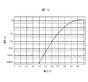
一方、過充電電圧保護機能が働いている間も有効となっている短絡電流保護機能に着目すると、例えば、短絡電流検出電圧V6を600mVとし、FET_CとFET_Dの直列オン抵抗を50mΩとした場合、FET_CとFET_Dが共にオン状態となる通常動作においては12Aの放電電流で短絡電流保護機能が働くことになる。しかしながら、この過充電電圧保護機能が働いた状態では、ボディーダイオードD1の電圧−電流特性が図11のようなものであったとすると、10mAの放電電流で短絡電流保護機能が働くことになる。この時の電池パックPBATの状態は、充電ができず、放電も10mA以上の放電電流が流れると電流を遮断するようになる。したがって、電流を流せる大きさが極端に減少したため、電池パックとして十分な機能を果たせない。これは、FET(FET_C,FET_D)のオン抵抗がある程度大きい場合には、その分、短絡電流検出電圧V6も高く設定され、結果的に、過充電電圧保護機能が働いている状態で流せる放電電流も十分に確保できるため特に大きな問題とはならない。しかしながら、FETのオン抵抗が低減されてくると、前述したように大きな問題を引き起こしてしまう。 On the other hand, paying attention to the short-circuit current protection function that is valid while the overcharge voltage protection function is working, for example, when the short-circuit current detection voltage V6 is 600 mV and the series on-resistance of FET_C and FET_D is 50 mΩ, In a normal operation in which both FET_C and FET_D are turned on, the short-circuit current protection function works with a discharge current of 12A. However, in a state where the overcharge voltage protection function is activated, if the voltage-current characteristic of the body diode D1 is as shown in FIG. 11, the short-circuit current protection function is activated at a discharge current of 10 mA. The state of the battery pack PBAT at this time cannot be charged, and the discharge is interrupted when a discharge current of 10 mA or more flows. Therefore, since the magnitude | size which can send an electric current decreased extremely, it cannot fulfill | perform a sufficient function as a battery pack. This is because when the on-resistance of the FETs (FET_C, FET_D) is large to some extent, the short-circuit current detection voltage V6 is also set higher accordingly, and as a result, the discharge current that can flow in the state where the overcharge voltage protection function is working. However, it is not a big problem because it can be secured sufficiently. However, if the on-resistance of the FET is reduced, it causes a big problem as described above.
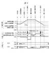
そこで、本実施の形態1の電池パックは、過充電電圧保護機能が働き、充電電流が遮断されてボディーダイオードD1を介した放電が行われる状態では、短絡電流保護機能の検出電圧をボディーダイオードD1の特性を考慮した特性に再設定することを特徴とする。図3は、図1の電池パックにおいて、その動作例を示すシーケンス図である。図3に示すシーケンスは、本実施の形態1の電池パックを用いることで、前述した図10のシーケンスを改良したものである。 Therefore, in the battery pack of the first embodiment, in the state where the overcharge voltage protection function works and the charge current is cut off and the discharge through the body diode D1 is performed, the detection voltage of the short circuit current protection function is set to the body diode D1. It is characterized in that it is reset to a characteristic that takes into account the characteristics. FIG. 3 is a sequence diagram showing an operation example of the battery pack of FIG. The sequence shown in FIG. 3 is obtained by improving the above-described sequence of FIG. 10 by using the battery pack of the first embodiment.
図3に示すように、二次電池BATに充電器を接続した後、BATの電圧値が過充電に該当する充電停止電圧V1に到達すると、それが一定の期間(Tsp3)継続するのを確認して、充電保護用FET(FET_C)がオフに制御される。ここで、FET_Cがオフに制御された際、監視IC(MIC)は、図10の場合と同様に、過放電電流保護機能(過放電電流検出電圧V5)を無効にする。これに加えて、監視IC(MIC)は、図10の場合と異なり、短絡電流検出電圧V6をV6[1]からそれよりも高いV6[2]に再設定する。具体的には、例えば、V6[1]=600mVとして、これをV6[2]=1.0Vに再設定する。この場合、図11のダイオード特性から判るように10A程度の電流が流れた際に短絡電流保護機能が働き、放電保護用FET(FET_D)がオフに制御されることになる。 As shown in FIG. 3, after the charger is connected to the secondary battery BAT, when the voltage value of BAT reaches the charge stop voltage V1 corresponding to overcharge, it is confirmed that it continues for a certain period (Tsp3). Then, the charge protection FET (FET_C) is controlled to be turned off. Here, when the FET_C is controlled to be turned off, the monitoring IC (MIC) invalidates the overdischarge current protection function (overdischarge current detection voltage V5) as in the case of FIG. In addition to this, unlike the case of FIG. 10, the monitoring IC (MIC) resets the short-circuit current detection voltage V6 from V6 [1] to V6 [2] higher than V6 [1]. Specifically, for example, V6 [1] = 600 mV, and this is reset to V6 [2] = 1.0V. In this case, as can be seen from the diode characteristics of FIG. 11, the short-circuit current protection function works when a current of about 10 A flows, and the discharge protection FET (FET_D) is controlled to be turned off.
その状態で、充電器を分離すると、電流値検出端子IDTにおいて正方向の電圧が検出される。この正方向の電圧は、監視IC(MIC)がIDTを介して充電器が分離されたことを認識するためにIDTから微小な電流を流出し、この電流が順方向のボディーダイオードD1を流れることで生じる。その後、二次電池BATに対して充電器に替わり負荷LDが接続されると、これに伴う放電電流によってIDTにおける正方向の電圧は更に上昇する。 When the charger is separated in this state, a positive voltage is detected at the current value detection terminal IDT. This positive voltage causes a small current to flow out of the IDT so that the monitoring IC (MIC) recognizes that the charger has been separated via the IDT, and this current flows through the body diode D1 in the forward direction. It occurs in. After that, when the load LD is connected to the secondary battery BAT instead of the charger, the positive voltage in the IDT further increases due to the discharge current associated therewith.
ここで、前述したように、短絡電流検出電圧V6がV6[1](600mV)であった場合には負荷LDに対して10mA程度の動作電流しか流すことができなかったが、V6[2](1.0V)に再設定することで、10A程度までの動作電流を流すことが可能となる。さらに、負荷LDにおいて、10A程度の動作電流が流れた場合には、それを短絡電流として検出し、当該電流を遮断することが可能となる。これによって、負荷LDに対して十分な動作電流を供給しつつも、電池パックPBATの安全性を適切に確保することが可能となる。また、前述したように、FET(FET_C,FET_D)の低オン抵抗化を進めることができ、電池パックの高効率化が図れるようになる。 Here, as described above, when the short-circuit current detection voltage V6 is V6 [1] (600 mV), only an operating current of about 10 mA can be supplied to the load LD, but V6 [2] By resetting to (1.0V), it becomes possible to flow an operating current of up to about 10A. Furthermore, when an operating current of about 10 A flows in the load LD, it can be detected as a short-circuit current and the current can be cut off. Accordingly, it is possible to appropriately ensure the safety of the battery pack PBAT while supplying a sufficient operating current to the load LD. Further, as described above, the on-resistance of the FETs (FET_C, FET_D) can be reduced, and the efficiency of the battery pack can be increased.
その後、図3に示すように、二次電池BATの電池電圧は、負荷LDの動作に伴う放電電流によって低下する。この電池電圧が充電停止復帰電圧V2まで低下すると、監視IC(MIC)は、充電保護用FET(FET_C)を再びオンに制御する。これによって、IDTの電圧は、負荷LDの動作電流に応じた正常な値まで低下する。また、監視IC(MIC)は、FET_Cを再びオンに制御した際に、過放電電流保護機能(過放電電流検出電圧V5)を有効に戻すと共に、短絡電流検出電圧V6もV6[2]からV6[1]に戻す。これによって、その後は、過放電電流保護機能も、適切に働くことになる。 Thereafter, as shown in FIG. 3, the battery voltage of the secondary battery BAT decreases due to the discharge current accompanying the operation of the load LD. When the battery voltage drops to the charge stop recovery voltage V2, the monitoring IC (MIC) controls the charge protection FET (FET_C) to be turned on again. As a result, the IDT voltage drops to a normal value corresponding to the operating current of the load LD. Further, when the monitoring IC (MIC) controls the FET_C to be turned on again, the monitoring IC (MIC) returns the overdischarge current protection function (overdischarge current detection voltage V5) to be effective, and the short circuit current detection voltage V6 is also changed from V6 [2] to V6. Return to [1]. As a result, the overdischarge current protection function also works properly thereafter.
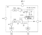
図4は、図1の電池パックにおいて、その監視ICの主要部の構成例を示す概略図である。図4に示す監視IC(MIC1)は、過充電系フラグ検出回路OCDETと、比較回路CMP1,CMP2と、駆動回路DRV1,DRV2と、期間判定回路TJGE1,TJGE2と、オア演算回路ORと、アンド演算回路ADと、定電圧回路VG_V5,VG_V6[1],VG_V6[2]と、セレクタ回路SEL1等を含んで構成される。 FIG. 4 is a schematic diagram showing a configuration example of a main part of the monitoring IC in the battery pack of FIG. The monitoring IC (MIC1) shown in FIG. 4 includes an overcharge flag detection circuit OCDET, comparison circuits CMP1 and CMP2, drive circuits DRV1 and DRV2, period determination circuits TJGE1 and TJGE2, an OR operation circuit OR, and an AND operation. The circuit AD includes constant voltage circuits VG_V5, VG_V6 [1], VG_V6 [2], a selector circuit SEL1, and the like.
過充電系フラグ検出回路OCDETは、図2および図3に示したように、電源電圧端子VCCからの電池電圧が充電停止電圧V1を超え、且つその状態がTsp3の期間継続した場合に‘H’レベルを出力する。その後、電池電圧が充電停止復帰電圧V2より低下した際には、この‘H’レベルを‘L’レベルに戻す。比較回路CMP1は、電流値検出端子IDTからの電圧と定電圧回路VG_V5からの過放電電流検出電圧V5とを比較し、IDT>V5の場合には‘H’レベルを出力する。アンド演算回路ADは、CMP1からの出力とOCDETからの反転出力とを演算し、期間判定回路TJGE1に出力を行う。TJGE1は、‘H’レベルの入力がTsp2の期間継続した場合に‘H’レベルを出力する。 As shown in FIGS. 2 and 3, the overcharge flag detection circuit OCDET is set to “H” when the battery voltage from the power supply voltage terminal VCC exceeds the charge stop voltage V1 and the state continues for the period of Tsp3. Output level. Thereafter, when the battery voltage drops below the charge stop recovery voltage V2, the 'H' level is returned to the 'L' level. The comparison circuit CMP1 compares the voltage from the current value detection terminal IDT with the overdischarge current detection voltage V5 from the constant voltage circuit VG_V5, and outputs “H” level when IDT> V5. The AND operation circuit AD calculates the output from CMP1 and the inverted output from OCDET, and outputs the result to the period determination circuit TJGE1. The TJGE1 outputs the “H” level when the input of the “H” level continues for the period of Tsp2.
一方、比較回路CMP2は、電流値検出端子IDTからの電圧とセレクタ回路SEL1を介した短絡電流検出電圧V6とを比較し、IDT>V6の場合には‘H’レベルを出力する。SEL1は、OCDETが‘L’レベルを出力している際には、図3で述べた電圧V6[1]を出力する定電圧回路VG_V6[1]を選択し、‘H’レベルを出力している際には、図3で述べた電圧V6[2]を出力する定電圧回路VG_V6[2]を選択する。期間判定回路TJGE2は、CMP2の‘H’レベル出力がTsp4の期間継続した場合に‘H’レベルを出力する。 On the other hand, the comparison circuit CMP2 compares the voltage from the current value detection terminal IDT with the short-circuit current detection voltage V6 via the selector circuit SEL1, and outputs “H” level when IDT> V6. SEL1 selects constant voltage circuit VG_V6 [1] that outputs voltage V6 [1] described in FIG. 3 when OCDET outputs 'L' level, and outputs 'H' level. The constant voltage circuit VG_V6 [2] that outputs the voltage V6 [2] described in FIG. 3 is selected. The period determination circuit TJGE2 outputs the “H” level when the “H” level output of CMP2 continues for the period of Tsp4.
オア演算回路ORは、TJGE1とTJGE2の出力を入力として演算し、駆動回路DRV2に出力を行う。DRV2は、ORの出力が‘L’レベルの場合には放電制御端子DCHを介して放電保護用FET(FET_D)をオンに制御し、ORの出力が‘H’レベルの場合にはDCHを介してFET_Dをオフに制御する。また、駆動回路DRV1は、過充電系フラグ検出回路OCDETの出力が‘L’レベルの場合には充電制御端子CHGを介して充電保護用FET(FET_C)をオンに制御し、OCDETの出力が‘H’レベルの場合にはCHGを介してFET_Cをオフに制御する。
The OR operation circuit OR calculates the outputs of TJGE1 and TJGE2 as inputs, and outputs them to the drive circuit DRV2. The
したがって、例えば、OCDETが‘H’レベルを出力している(すなわち過充電状態が検出されている)間は、CMP1の出力に関わらず、ADおよびTJGE1から‘L’レベルが出力され、FET_Dのオン・オフは、CMP2およびTJGE2の出力に応じて定められる。すなわち、過放電電流保護機能は無効となる。また、この間、CMP2は、IDTの電圧をV6[2]を基準に判定し、IDT>V6[2]の状態がTsp4の間継続した場合(短絡電流検出時)には、TJGE2から‘H’レベルが出力され、そうでない場合には、TJGE2から‘L’レベルが出力される。FET_Dは、TJGE2の‘H’レベルに応じてオフに制御され、‘L’レベルに応じてオンを維持する。一方、OCDETが‘L’レベルを出力している間は、IDT>V5の状態がTsp2の間継続した場合(過放電電流検出時)か、IDT>V6[1]の状態がTsp4の間継続した場合(短絡電流検出時)にFET_Dがオフに制御される。つまり、短絡電流保護機能に加えて過放電電流保護機能も有効となる。 Therefore, for example, while OCDET is outputting the “H” level (that is, the overcharge state is detected), the “L” level is output from AD and TJGE1 regardless of the output of CMP1, and the FET_D ON / OFF is determined according to the outputs of CMP2 and TJGE2. That is, the overdischarge current protection function is disabled. During this time, the CMP2 determines the IDT voltage with reference to V6 [2], and when the state of IDT> V6 [2] continues for Tsp4 (at the time of detecting the short-circuit current), the TJGE2 determines “H”. If the level is output, otherwise, the “L” level is output from TJGE2. The FET_D is controlled to be turned off according to the “H” level of the TJGE2, and is kept on according to the “L” level. On the other hand, while OCDET outputs 'L' level, the state of IDT> V5 continues for Tsp2 (when overdischarge current is detected) or the state of IDT> V6 [1] continues for Tsp4. FET_D is controlled to be turned off in the case (when short circuit current is detected). That is, in addition to the short-circuit current protection function, the overdischarge current protection function is also effective.
図5は、図10の動作を行う電池パック(前提システム)と図3の動作を行う電池パック(提案システム)とでその主な仕様の一例を比較した表である。図5に示すように、過充電状態に伴い充電保護用FETがオフ、放電保護用FETがオンとなっている間、前提システムでは短絡電流検出電圧が例えば600mVであったが、提案システムでは例えば1000mVに変更されている。 FIG. 5 is a table comparing an example of main specifications of the battery pack (premise system) that performs the operation of FIG. 10 and the battery pack (proposed system) that performs the operation of FIG. As shown in FIG. 5, while the charge protection FET is turned off and the discharge protection FET is turned on in the overcharge state, the short-circuit current detection voltage is 600 mV in the premise system, for example, but in the proposed system, for example, It has been changed to 1000 mV.
以上、本発明の実施の形態1による電池パックを用いることで、代表的には、二次電池の安全性を適切に確保することが可能となる。また、充電および放電スイッチの低オン抵抗化が図れ、高効率な電池パックを実現可能になる。
As described above, typically, by using the battery pack according to
(実施の形態2)
図6は、本発明の実施の形態2による電池パックにおいて、その動作例を示すシーケンス図である。本実施の形態2の電池パックの構成は、図1と同様である。図6に示すシーケンスは、前述した図3のシーケンスと比較して、短絡電流検出電圧V6に加えて過放電電流検出電圧V5も再設定されている点が異なっている。それ以外の点に関しては、図3と同様であるため詳細な説明は省略する。
(Embodiment 2)
FIG. 6 is a sequence diagram showing an operation example of the battery pack according to
図6に示すように、過充電電圧の検出に伴い充電保護用FET(FET_C)がオフに制御された際、監視IC(MIC)は、図3の場合と同様に、短絡電流検出電圧V6をV6[1](例えば600mV)からV6[2](例えば1.0V)に再設定する。これに加えて、監視IC(MIC)は、図3の場合と異なり、過放電電流検出電圧V5をV5[1]からそれよりも高いV5[2]に再設定する。具体的には、例えば、V5[1]=100mVとして、これをV5[2]=0.8Vに再設定する。なお、過充電電圧の検出前におけるV5[1]=100mVの場合には、FET_CおよびFET_Dの直列オン抵抗を50mΩとして、放電電流が2A流れた際に過放電と判断される。 As shown in FIG. 6, when the charge protection FET (FET_C) is controlled to be turned off along with the detection of the overcharge voltage, the monitoring IC (MIC) sets the short-circuit current detection voltage V6 as in the case of FIG. Reset from V6 [1] (for example, 600 mV) to V6 [2] (for example, 1.0 V). In addition, unlike the case of FIG. 3, the monitoring IC (MIC) resets the overdischarge current detection voltage V5 from V5 [1] to V5 [2] higher than V5 [1]. Specifically, for example, V5 [1] = 100 mV, and this is reset to V5 [2] = 0.8V. When V5 [1] = 100 mV before detection of the overcharge voltage, it is determined that overdischarge occurs when a discharge current of 2 A flows with the series on resistance of FET_C and FET_D set to 50 mΩ.
その状態で、充電器を分離すると、電流値検出端子IDTにおいて正方向の電圧が検出される。この正方向の電圧は、監視IC(MIC)がIDTを介して充電器が分離されたことを認識するためにIDTから微小な電流を流出し、この電流が順方向のボディーダイオードD1を流れることで生じる。この微小な電流が例えば0.1μA程度であった場合、図11のダイオード特性からIDTの電圧は例えば300mV程度となる恐れがある。ここで、過放電電流検出電圧V5が仮にV5[1](100mV)のままであった場合には、過放電電流の検出と判断され、放電保護用FET(FET_D)がオフに制御されるが、V5をV5[2](0.8V)に再設定することで、過放電電流の検出電流値を1A程度にすることが可能となり、FET_Dのオン状態を維持できる。 When the charger is separated in this state, a positive voltage is detected at the current value detection terminal IDT. This positive voltage causes a small current to flow out of the IDT so that the monitoring IC (MIC) recognizes that the charger has been separated via the IDT, and this current flows through the body diode D1 in the forward direction. It occurs in. When this minute current is, for example, about 0.1 μA, the IDT voltage may be, for example, about 300 mV from the diode characteristics of FIG. Here, if the overdischarge current detection voltage V5 remains V5 [1] (100 mV), it is determined that the overdischarge current is detected, and the discharge protection FET (FET_D) is controlled to be turned off. By resetting V5 to V5 [2] (0.8V), it becomes possible to set the detection current value of the overdischarge current to about 1 A, and the FET_D can be kept on.
その後、二次電池BATに対して充電器に替わり負荷LDが接続されると、これに伴う放電電流によってIDTにおける正方向の電圧は更に上昇する。この際に、監視ICは、V5[2]とV6[2]に伴い、負荷LDの動作電流が1A程度に達すると過放電電流と判断し、10A程度に達すると短絡電流と判断する。したがって、負荷LDに対して十分な動作電流を供給しつつ、過放電電流と短絡電流を適切に検出することができ、電池パックPBATの安全性を適切に確保することが可能となる。また、前述したように、FET(FET_C,FET_D)の低オン抵抗化を進めることができ、電池パックの高効率化が図れるようになる。 After that, when the load LD is connected to the secondary battery BAT instead of the charger, the positive voltage in the IDT further increases due to the discharge current associated therewith. At this time, the monitoring IC determines that the operating current of the load LD reaches about 1 A along with V5 [2] and V6 [2], and determines that it is a short-circuit current when it reaches about 10 A. Therefore, the overdischarge current and the short-circuit current can be appropriately detected while supplying a sufficient operating current to the load LD, and the safety of the battery pack PBAT can be appropriately ensured. Further, as described above, the on-resistance of the FETs (FET_C, FET_D) can be reduced, and the efficiency of the battery pack can be increased.
その後、図6に示すように、二次電池BATの電池電圧は、負荷LDの動作に伴う放電電流によって低下する。この電池電圧が充電停止復帰電圧V2まで低下すると、監視IC(MIC)は、充電保護用FET(FET_C)を再びオンに制御する。これによって、IDTの電圧は、負荷LDの動作電流に応じた正常な値まで低下する。また、監視IC(MIC)は、FET_Cを再びオンに制御した際に、過放電電流検出電圧V5をV5[2]からV5[1]に戻すと共に、短絡電流検出電圧V6もV6[2]からV6[1]に戻す。これによって、その後も、過放電電流保護機能および短絡電流保護機能共に、適切に働くことになる。 Thereafter, as shown in FIG. 6, the battery voltage of the secondary battery BAT decreases due to the discharge current accompanying the operation of the load LD. When the battery voltage drops to the charge stop recovery voltage V2, the monitoring IC (MIC) controls the charge protection FET (FET_C) to be turned on again. As a result, the IDT voltage drops to a normal value corresponding to the operating current of the load LD. When the monitoring IC (MIC) controls the FET_C to be turned on again, the monitoring IC (MIC) returns the overdischarge current detection voltage V5 from V5 [2] to V5 [1], and the short-circuit current detection voltage V6 also changes from V6 [2]. Return to V6 [1]. As a result, both the overdischarge current protection function and the short-circuit current protection function work properly thereafter.
図7は、本発明の実施の形態2による電池パックにおいて、図1の電池パックにおける監視ICの主要部の構成例を示す概略図である。図7に示す監視IC(MIC2)は、図4に示した監視IC(MIC1)と比較して、オア演算回路ORの一方の入力に接続される過放電電流検出系の回路構成が異なっている。ORの他方の入力に接続される短絡電流検出系の回路構成(定電圧回路VG_V6[1],VG_V6[2]、セレクタ回路SEL1、比較回路CMP2、期間判定回路TJGE2)や、過充電系フラグ検出回路OCDETならびに駆動回路DRV1,DRV2の機能に関しては、図4と同様であるため詳細な説明は省略する。 FIG. 7 is a schematic diagram illustrating a configuration example of a main part of the monitoring IC in the battery pack of FIG. 1 in the battery pack according to the second embodiment of the present invention. The monitoring IC (MIC2) shown in FIG. 7 differs from the monitoring IC (MIC1) shown in FIG. 4 in the circuit configuration of the overdischarge current detection system connected to one input of the OR operation circuit OR. . Circuit configuration of short-circuit current detection system connected to the other input of OR (constant voltage circuits VG_V6 [1], VG_V6 [2], selector circuit SEL1, comparison circuit CMP2, period determination circuit TJGE2), and overcharge flag detection The functions of the circuit OCDET and the drive circuits DRV1 and DRV2 are the same as those in FIG.
過放電電流検出系の回路は、短絡電流検出系の回路と同様に、定電圧回路VG_V5[1],VG_V5[2]と、セレクタ回路SEL2と、比較回路CMP1と、期間判定回路TJGE1によって構成される。比較回路CMP1は、電流値検出端子IDTからの電圧とセレクタ回路SEL2を介した過放電電流検出電圧V5とを比較し、IDT>V5の場合には‘H’レベルを出力する。SEL2は、OCDETが‘L’レベルを出力している際には、図6で述べた電圧V5[1]を出力する定電圧回路VG_V5[1]を選択し、‘H’レベルを出力している際には、図6で述べた電圧V5[2]を出力する定電圧回路VG_V5[2]を選択する。期間判定回路TJGE1は、CMP1の‘H’レベル出力がTsp2の期間継続した場合に‘H’レベルを出力する。 Similar to the short-circuit current detection system circuit, the overdischarge current detection system circuit includes constant voltage circuits VG_V5 [1], VG_V5 [2], a selector circuit SEL2, a comparison circuit CMP1, and a period determination circuit TJGE1. The The comparison circuit CMP1 compares the voltage from the current value detection terminal IDT with the overdischarge current detection voltage V5 via the selector circuit SEL2, and outputs 'H' level when IDT> V5. SEL2 selects constant voltage circuit VG_V5 [1] that outputs voltage V5 [1] described in FIG. 6 when OCDET outputs 'L' level, and outputs 'H' level. The constant voltage circuit VG_V5 [2] that outputs the voltage V5 [2] described in FIG. 6 is selected. The period determination circuit TJGE1 outputs the “H” level when the “H” level output of CMP1 continues for the period of Tsp2.
したがって、例えば、OCDETが‘H’レベルを出力している(すなわち過充電状態が検出されている)間、IDT>V5[2]の状態がTsp2の間継続するか、あるいはIDT>V6[2]の状態がTsp4の間継続すると、オア演算回路ORならびに駆動回路DRV2を介して放電保護用FET(FET_D)がオフに制御される。一方、OCDETが‘L’レベルを出力している間は、IDT>V5[1]の状態がTsp2の間継続するか、あるいはIDT>V6[1]の状態がTsp4の間継続すると、ORならびにDRV2を介してFET_Dがオフに制御される。 Therefore, for example, while OCDET outputs “H” level (that is, an overcharge state is detected), the state of IDT> V5 [2] continues for Tsp2, or IDT> V6 [2 ] Continues for Tsp4, the discharge protection FET (FET_D) is controlled to be turned off via the OR operation circuit OR and the drive circuit DRV2. On the other hand, while OCDET is outputting the “L” level, if the state of IDT> V5 [1] continues for Tsp2, or if the state of IDT> V6 [1] continues for Tsp4, OR and FET_D is controlled to be turned off via DRV2.
図8は、図10の動作を行う電池パック(前提システム)と図6の動作を行う電池パック(提案システム)とでその主な仕様の一例を比較した表である。図8に示すように、過充電状態に伴い充電保護用FETがオフ、放電保護用FETがオンとなっている間、前提システムでは短絡電流検出電圧が例えば600mVであったが、提案システムでは例えば1000mVに変更されている。さらに、前提システムでは、過放電電流検出機能が無効であったが、提案システムでは有効とされ、過放電電流検出電圧が例えば800mVに設定されている。 FIG. 8 is a table comparing an example of main specifications of the battery pack (premise system) that performs the operation of FIG. 10 and the battery pack (proposed system) that performs the operation of FIG. As shown in FIG. 8, while the charge protection FET is turned off and the discharge protection FET is turned on in the overcharge state, the short-circuit current detection voltage is 600 mV in the premise system, for example, but in the proposed system, for example, It has been changed to 1000 mV. Furthermore, although the overdischarge current detection function is invalid in the premise system, it is valid in the proposed system, and the overdischarge current detection voltage is set to 800 mV, for example.
このように、本実施の形態2の電池パックは、前述した実施の形態1の電池パックと比較して、過充電状態が検出されている間、短絡電流の検出に加えて過放電電流の検出も可能な構成となっている。これらの検出条件は、それぞれ、電流値(IDTでの検出電圧)とその継続期間(スパイク回避時間Tsp)の組み合わせで定められる。例えば、短絡電流の検出条件では、電流値が高く設定されるがその分継続期間が短く設定され、これによって電池パックの破壊を防止する。また、過放電電流の検出条件では、電流値が負荷の正常な駆動電流よりも若干高い値に設定されるが、一時的なピーク電流等を加味して継続期間が長く設定され、これによって、異常な負荷から前もって電池パックを保護する。 As described above, the battery pack according to the second embodiment is compared with the battery pack according to the first embodiment described above, while detecting the overdischarge current in addition to the detection of the short-circuit current while the overcharge state is detected. Is also possible. Each of these detection conditions is determined by a combination of a current value (detection voltage at IDT) and its duration (spike avoidance time Tsp). For example, under the short-circuit current detection condition, the current value is set high, but the duration is set shorter, thereby preventing the battery pack from being destroyed. Further, in the overdischarge current detection condition, the current value is set to a value slightly higher than the normal drive current of the load, but the duration is set to be long in consideration of the temporary peak current, etc. Protect the battery pack in advance from abnormal loads.
このように、電流値とその継続期間の組み合わせからなる安全動作領域を複数設定することで電池パックの適切な保護が図れる。ここで、前述した実施の形態1では、過放電電流保護機能を一時的に無効にしているが、これは電池パックの破壊といった致命的な問題には到らず、また、その後に過充電状態から回復した際に再び有効とされるため、実質的に電池パックの適切な保護は可能である。ただし、より安全性を高めたい場合には、本実施の形態2の構成を用いて、過充電状態の間も過放電電流保護機能を有効とすればよい。 As described above, the battery pack can be appropriately protected by setting a plurality of safe operation areas including combinations of current values and durations thereof. Here, in the first embodiment described above, the overdischarge current protection function is temporarily disabled, but this does not lead to a fatal problem such as destruction of the battery pack, and after that, the overcharge state Since it is re-enabled when recovered from the battery, a substantial protection of the battery pack is substantially possible. However, when it is desired to further improve safety, the overdischarge current protection function may be enabled even during the overcharge state using the configuration of the second embodiment.
以上、本発明の実施の形態2による電池パックを用いることで、代表的には、二次電池の安全性を適切に確保することが可能となる。また、充電および放電スイッチの低オン抵抗化が図れ、高効率な電池パックを実現可能になる。 As described above, typically, by using the battery pack according to the second embodiment of the present invention, it is possible to appropriately ensure the safety of the secondary battery. In addition, the on-resistance of the charge and discharge switches can be reduced, and a highly efficient battery pack can be realized.
以上、本発明者によってなされた発明を実施の形態に基づき具体的に説明したが、本発明は前記実施の形態に限定されるものではなく、その要旨を逸脱しない範囲で種々変更可能である。 As mentioned above, the invention made by the present inventor has been specifically described based on the embodiments. However, the present invention is not limited to the above-described embodiments, and various modifications can be made without departing from the scope of the invention.
例えば、前述した実施の形態では、便宜上、過充電電圧保護機能が働く前後で電流の検出値を違う値(例えば、短絡電流検出値を12A→10A)にしたが、勿論、同じ値にすることも可能である。さらに、この電流値を任意に設定できる構成とすることも可能である。この場合、例えば図7の定電圧回路VG_V5[1],VG_V5[2],VG_V6[1],VG_V6[2]を、半導体ヒューズ等によって電圧設定が可能な可変電圧回路とすればよい。 For example, in the above-described embodiment, for convenience, the current detection value is set to a different value (for example, the short-circuit current detection value is 12A → 10A) before and after the overcharge voltage protection function operates. Is also possible. Furthermore, a configuration in which this current value can be arbitrarily set is also possible. In this case, for example, the constant voltage circuits VG_V5 [1], VG_V5 [2], VG_V6 [1], and VG_V6 [2] in FIG. 7 may be variable voltage circuits that can be set with a semiconductor fuse or the like.
また、前述した実施の形態では、充電保護用および放電保護用スイッチとしてFETを用いたが、これに限らず例えばバイポーラトランジスタ等を用いることも可能である。さらに、前述した実施の形態では、マイナス端子側の電流経路に充電保護用および放電保護用スイッチが挿入された構成例を示したが、例えば当該スイッチがプラス端子側の電流経路に挿入された構成も考えられ、本実施の形態は、このような構成に対しても同様に適用可能である。 In the above-described embodiment, the FET is used as the charge protection switch and the discharge protection switch. However, the present invention is not limited to this. For example, a bipolar transistor or the like can be used. Furthermore, in the above-described embodiment, the configuration example in which the charge protection and discharge protection switches are inserted in the current path on the negative terminal side is shown. For example, the configuration in which the switch is inserted in the current path on the positive terminal side is shown. The present embodiment can be similarly applied to such a configuration.
本実施の形態による電池パックは、特に、携帯電話機等のモバイル機器に使用されるリチウムイオン二次電池パックに適用して有益な技術であり、これに限らず、ノートパソコン等のようにバッテリを搭載する機器全般に対して広く適用可能である。 The battery pack according to the present embodiment is a technology that is particularly useful when applied to lithium ion secondary battery packs used in mobile devices such as mobile phones, and is not limited to this. The present invention can be widely applied to all installed devices.
PBAT 電池パック
BAT 二次電池
MIC 監視IC
R 抵抗
LD 負荷
BC 充電器
FETCP FETチップ
B(+),P(+) プラス端子
B(−),P(−) マイナス端子
FET_D 放電保護用FET
FET_C 充電保護用FET
D ボディーダイオード
VCC 電源電圧端子
GND 基準電源電圧端子
IDT 電流値検出端子
DCH 放電制御端子
CHG 充電制御端子
BBD 配線基板
CMP 比較回路
TJGE 期間判定回路
OR オア演算回路
AD アンド演算回路
VG 定電圧回路
DRV 駆動回路
OCDET 過充電系フラグ検出回路
SEL セレクタ回路
PBAT Battery pack BAT Secondary battery MIC Monitoring IC
R resistance LD load BC charger FETCP FET chip B (+), P (+) Positive terminal B (-), P (-) Negative terminal FET_D FET for discharge protection
FET_C Charge protection FET
D body diode VCC power supply voltage terminal GND reference power supply voltage terminal IDT current value detection terminal DCH discharge control terminal CHG charge control terminal BBD wiring board CMP comparison circuit TJGE period determination circuit OR OR operation circuit AD and operation circuit VG constant voltage circuit DRV drive circuit OCDET Overcharge flag detection circuit SEL selector circuit
Claims (12)
検出端子と、
第1および第2制御端子と、
前記第1制御端子によってオン・オフが制御され、電流経路となる2つのノードの一方が前記検出端子と導通する第1トランジスタと、
前記第2制御端子によってオン・オフが制御され、電流経路となる2つのノードの一方が前記第2電源端子と導通し、他方が前記第1トランジスタの2つのノードの他方に接続された第2トランジスタと、
前記第1トランジスタの2つのノード間に接続され、前記検出端子側をアノードとする第1ダイオードと、
前記第2トランジスタの2つのノード間に接続され、前記第2電源端子側をアノードとする第2ダイオードと、
前記第1および第2制御端子を介して前記第1および第2トランジスタのオン・オフを制御する制御回路とを備え、
前記制御回路は、
前記第1および第2トランジスタを共にオンに制御している際には、前記第2電源端子の電圧を基準に前記検出端子で検出した検出電圧が第1A判定電圧に達し、且つその状態が第1期間継続した場合に前記第2トランジスタをオフに制御し、
前記第1トランジスタをオフ、前記第2トランジスタをオンに制御している際には、前記検出電圧が前記第1A判定電圧よりも大きい第1B判定電圧に達し、且つその状態が前記第1期間継続した場合に前記第2トランジスタをオフに制御することを特徴とする電池制御装置。 First and second power supply terminals;
A detection terminal;
First and second control terminals;
A first transistor which is controlled to be turned on and off by the first control terminal, and one of two nodes serving as a current path is electrically connected to the detection terminal;
On / off is controlled by the second control terminal, one of two nodes serving as a current path is electrically connected to the second power supply terminal, and the other is connected to the other of the two nodes of the first transistor. A transistor,
A first diode connected between two nodes of the first transistor and having the detection terminal side as an anode;
A second diode connected between two nodes of the second transistor and having the second power supply terminal side as an anode;
A control circuit for controlling on / off of the first and second transistors via the first and second control terminals,
The control circuit includes:
When both the first and second transistors are controlled to be on, the detection voltage detected at the detection terminal with reference to the voltage of the second power supply terminal reaches the first A determination voltage, and the state is the first Controlling the second transistor off when continued for one period;
When the first transistor is controlled to be off and the second transistor is controlled to be on, the detection voltage reaches a first B determination voltage that is higher than the first A determination voltage, and the state continues for the first period. In this case, the battery control device controls the second transistor to be turned off.
前記制御回路は、更に、前記第1および第2トランジスタを共にオンに制御している際には、前記検出電圧が第2A判定電圧に達し、且つその状態が第2期間継続した場合に前記第2トランジスタをオフに制御し、
前記第2A判定電圧は、前記第1A判定電圧よりも小さく、
前記第2期間は、前記第1期間よりも長いことを特徴とする電池制御装置。 The battery control device according to claim 1,
The control circuit further controls the first and second transistors to turn on when the detection voltage reaches the second A determination voltage and the state continues for a second period. Control 2 transistors off,
The second A determination voltage is smaller than the first A determination voltage,
The battery control apparatus, wherein the second period is longer than the first period.
前記制御回路は、更に、前記第1トランジスタをオフ、前記第2トランジスタをオンに制御している際には、前記検出電圧が前記第2A判定電圧よりも大きい第2B判定電圧に達し、且つその状態が前記第2期間継続した場合に前記第2トランジスタをオフに制御することを特徴とする電池制御装置。 The battery control device according to claim 2,
When the control circuit further controls the first transistor to be turned off and the second transistor to be turned on, the detection voltage reaches a second B determination voltage that is greater than the second A determination voltage, and The battery control device, wherein the second transistor is controlled to be turned off when the state continues for the second period.
前記制御回路は、前記第2電源端子の電圧を基準に前記第1電源端子の電圧が第3A判定電圧に達し、且つその状態が第3期間継続した場合に前記第1トランジスタをオフ、前記第2トランジスタをオンに制御し、その後、前記第1電源端子の電圧が前記第3A判定電圧よりも小さい第3B判定電圧に戻った場合に前記第1および第2トランジスタを共にオンに制御することを特徴とする電池制御装置。 The battery control device according to claim 2,
The control circuit turns off the first transistor when the voltage of the first power supply terminal reaches the third A determination voltage with reference to the voltage of the second power supply terminal and the state continues for a third period, 2 transistors are turned on, and then the first and second transistors are both turned on when the voltage of the first power supply terminal returns to the third B determination voltage smaller than the third A determination voltage. A battery control device.
正極ノードおよび負極ノードを備えた二次電池と、
第1および第2電源ノード、検出ノード、第1および第2制御ノードを備えた制御回路と、
第1および第2トランジスタと、
第1および第2ダイオードとを有し、
前記正極外部端子と前記正極ノードは、共通接続されると共に前記第1電源ノードに導通し、
前記第1トランジスタは、前記第1制御ノードによってオン・オフが制御され、電流経路となる2つのノードの一方が前記検出ノードに導通すると共に前記負極外部端子に接続され、
前記第2トランジスタは、前記第2制御ノードによってオン・オフが制御され、電流経路となる2つのノードの一方が前記第2電源ノードに導通すると共に前記負極ノードに接続され、他方が前記第1トランジスタの2つのノードの他方に接続され、
前記第1ダイオードは、前記第1トランジスタの2つのノード間に、前記負極外部端子側をアノードとして接続され、
前記第2ダイオードは、前記第2トランジスタの2つのノード間に、前記負極ノード側をアノードとして接続され、
前記制御回路は、
前記第1および第2トランジスタを共にオンに制御している際には、前記第2電源ノードの電圧を基準に前記検出ノードで検出した検出電圧が第1A判定電圧に達し、且つその状態が第1期間継続した場合に前記第2トランジスタをオフに制御し、
前記第1トランジスタをオフ、前記第2トランジスタをオンに制御している際には、前記検出電圧が前記第1A判定電圧よりも大きい第1B判定電圧に達し、且つその状態が前記第1期間継続した場合に前記第2トランジスタをオフに制御することを特徴とする電池パック。 A positive external terminal and a negative external terminal;
A secondary battery having a positive node and a negative node;
A control circuit comprising first and second power supply nodes, a detection node, first and second control nodes;
First and second transistors;
First and second diodes;
The positive external terminal and the positive node are commonly connected and conducted to the first power supply node,
The first transistor is controlled to be turned on / off by the first control node, and one of two nodes serving as a current path is connected to the detection node and connected to the negative external terminal,
The second transistor is controlled to be turned on / off by the second control node, and one of two nodes serving as a current path is connected to the second power supply node and connected to the negative node, and the other is connected to the first node. Connected to the other of the two nodes of the transistor;
The first diode is connected between two nodes of the first transistor with the negative external terminal side as an anode,
The second diode is connected between two nodes of the second transistor with the negative node side as an anode,
The control circuit includes:
When both the first and second transistors are controlled to be on, the detection voltage detected at the detection node with respect to the voltage of the second power supply node reaches the first A determination voltage, and the state is the first Controlling the second transistor off when continued for one period;
When the first transistor is controlled to be off and the second transistor is controlled to be on, the detection voltage reaches a first B determination voltage that is higher than the first A determination voltage, and the state continues for the first period. In this case, the battery pack is controlled to turn off the second transistor.
前記制御回路は、更に、前記第1および第2トランジスタを共にオンに制御している際には、前記検出電圧が第2A判定電圧に達し、且つその状態が第2期間継続した場合に前記第2トランジスタをオフに制御し、
前記第2A判定電圧は、前記第1A判定電圧よりも小さく、
前記第2期間は、前記第1期間よりも長いことを特徴とする電池パック。 The battery pack according to claim 5, wherein
The control circuit further controls the first and second transistors to turn on when the detection voltage reaches the second A determination voltage and the state continues for a second period. Control 2 transistors off,
The second A determination voltage is smaller than the first A determination voltage,
The battery pack, wherein the second period is longer than the first period.
前記制御回路は、更に、前記第1トランジスタをオフ、前記第2トランジスタをオンに制御している際には、前記検出電圧が前記第2A判定電圧よりも大きい第2B判定電圧に達し、且つその状態が前記第2期間継続した場合に前記第2トランジスタをオフに制御することを特徴とする電池パック。 The battery pack according to claim 6, wherein
When the control circuit further controls the first transistor to be turned off and the second transistor to be turned on, the detection voltage reaches a second B determination voltage that is greater than the second A determination voltage, and The battery pack, wherein the second transistor is controlled to be turned off when the state continues for the second period.
前記制御回路は、前記第2電源ノードの電圧を基準に前記第1電源ノードの電圧が第3A判定電圧に達し、且つその状態が第3期間継続した場合に前記第1トランジスタをオフ、前記第2トランジスタをオンに制御し、その後、前記第1電源ノードの電圧が前記第3A判定電圧よりも小さい第3B判定電圧に戻った場合に前記第1および第2トランジスタを共にオンに制御することを特徴とする電池パック。 The battery pack according to claim 6, wherein
The control circuit turns off the first transistor when the voltage of the first power supply node reaches the 3A determination voltage with reference to the voltage of the second power supply node and the state continues for a third period, Two transistors are turned on, and then the first and second transistors are both turned on when the voltage of the first power supply node returns to the third B determination voltage smaller than the third A determination voltage. Battery pack featuring.
前記第1Aおよび第1B判定電圧は、前記正極外部端子と前記負極外部端子の間が短絡状態とみなされる場合を検出する電圧であり、
前記第2Aおよび第2B判定電圧は、前記正極外部端子から前記負極外部端子に向けて過剰電流が流れた場合を検出する電圧であることを特徴とする電池パック。 The battery pack according to claim 8, wherein
The 1A and 1B determination voltages are voltages for detecting a case where a short circuit state is assumed between the positive external terminal and the negative external terminal,
The battery pack according to claim 2, wherein the second A and second B determination voltages are voltages for detecting a case where an excessive current flows from the positive external terminal toward the negative external terminal.
前記充電保護用スイッチに並列接続され、前記二次電池からの放電電流のみを流す第1ダイオードと、
前記放電保護用スイッチに並列接続され、前記二次電池への充電電流のみを流す第2ダイオードと、
前記二次電池の電圧および電流を監視し、前記充電保護用スイッチおよび前記放電保護用スイッチのオン・オフを制御する制御回路とを備え、
前記制御回路は、
前記充電保護用スイッチおよび前記放電保護用スイッチを共にオンに制御している際には、前記第1ノードと前記第2ノード間の電位差が第1A判定電圧に達し、且つその状態が第1期間継続した場合に前記放電保護用スイッチをオフに制御し、
前記充電保護用スイッチをオフ、前記放電保護用スイッチをオンに制御している際には、前記第1ノードと前記第2ノード間の電位差が前記第1A判定電圧よりも大きい第1B判定電圧に達し、且つその状態が前記第1期間継続した場合に前記放電保護用スイッチをオフに制御することを特徴とする電池制御装置。 A charge protection switch and a discharge protection switch inserted in series between the first and second nodes on the charge / discharge current path of the secondary battery;
A first diode connected in parallel to the charge protection switch and allowing only a discharge current from the secondary battery to flow;
A second diode connected in parallel to the discharge protection switch and allowing only a charging current to the secondary battery to flow;
A control circuit that monitors the voltage and current of the secondary battery and controls on / off of the charge protection switch and the discharge protection switch;
The control circuit includes:
When both the charge protection switch and the discharge protection switch are turned on, the potential difference between the first node and the second node reaches the first A determination voltage, and the state is in the first period. If it continues, control the switch for discharge protection off,
When the charge protection switch is turned off and the discharge protection switch is turned on, the potential difference between the first node and the second node is set to a first B determination voltage that is larger than the first A determination voltage. The battery control device is configured to control the discharge protection switch to be turned off when the state is reached and the state continues for the first period.
前記制御回路は、更に、前記充電保護用スイッチおよび前記放電保護用スイッチを共にオンに制御している際には、前記第1ノードと前記第2ノード間の電位差が第2A判定電圧に達し、且つその状態が第2期間継続した場合に前記放電保護用スイッチをオフに制御し、
前記第2A判定電圧は、前記第1A判定電圧よりも小さく、
前記第2期間は、前記第1期間よりも長いことを特徴とする電池制御装置。 The battery control device according to claim 10, wherein
When the control circuit further controls to turn on both the charge protection switch and the discharge protection switch, the potential difference between the first node and the second node reaches a second A determination voltage, And when the state continues for the second period, the discharge protection switch is controlled to be turned off,
The second A determination voltage is smaller than the first A determination voltage,
The battery control apparatus, wherein the second period is longer than the first period.
前記制御回路は、更に、前記充電保護用スイッチをオフ、前記放電保護用スイッチをオンに制御している際には、前記第1ノードと前記第2ノード間の電位差が前記第2A判定電圧よりも大きい第2B判定電圧に達し、且つその状態が前記第2期間継続した場合に前記放電保護用スイッチをオフに制御することを特徴とする電池制御装置。 The battery control device according to claim 11, wherein
When the control circuit further controls the charge protection switch to be turned off and the discharge protection switch to be turned on, a potential difference between the first node and the second node is greater than the second A determination voltage. A battery control device that controls the discharge protection switch to be off when the second 2B determination voltage is reached and the state continues for the second period.
Priority Applications (1)
| Application Number | Priority Date | Filing Date | Title |
|---|---|---|---|
| JP2009170054A JP2011030283A (en) | 2009-07-21 | 2009-07-21 | Battery controller and battery pack |
Applications Claiming Priority (1)
| Application Number | Priority Date | Filing Date | Title |
|---|---|---|---|
| JP2009170054A JP2011030283A (en) | 2009-07-21 | 2009-07-21 | Battery controller and battery pack |
Publications (2)
| Publication Number | Publication Date |
|---|---|
| JP2011030283A true JP2011030283A (en) | 2011-02-10 |
| JP2011030283A5 JP2011030283A5 (en) | 2012-02-02 |
Family
ID=43638366
Family Applications (1)
| Application Number | Title | Priority Date | Filing Date |
|---|---|---|---|
| JP2009170054A Withdrawn JP2011030283A (en) | 2009-07-21 | 2009-07-21 | Battery controller and battery pack |
Country Status (1)
| Country | Link |
|---|---|
| JP (1) | JP2011030283A (en) |
Cited By (1)
| Publication number | Priority date | Publication date | Assignee | Title |
|---|---|---|---|---|
| CN106385066A (en) * | 2016-09-23 | 2017-02-08 | 宇龙计算机通信科技(深圳)有限公司 | Charging and discharging circuit of battery and terminal |
Citations (5)
| Publication number | Priority date | Publication date | Assignee | Title |
|---|---|---|---|---|
| JPH10229636A (en) * | 1997-02-14 | 1998-08-25 | Seiko Instr Inc | Charge and discharge control circuit |
| JP2002176730A (en) * | 2000-09-28 | 2002-06-21 | Ricoh Co Ltd | Charge/discharge protective circuit, battery pack incorporating the same, and electronic apparatus using the battery pack |
| JP2003169422A (en) * | 2001-11-30 | 2003-06-13 | Sanyo Electric Co Ltd | Overcurrent protective circuit for battery |
| JP2003189480A (en) * | 2001-12-20 | 2003-07-04 | Mitsubishi Cable Ind Ltd | Protective circuit of secondary battery |
| JP2006254650A (en) * | 2005-03-14 | 2006-09-21 | Mitsumi Electric Co Ltd | Battery protection circuit |
-
2009
- 2009-07-21 JP JP2009170054A patent/JP2011030283A/en not_active Withdrawn
Patent Citations (5)
| Publication number | Priority date | Publication date | Assignee | Title |
|---|---|---|---|---|
| JPH10229636A (en) * | 1997-02-14 | 1998-08-25 | Seiko Instr Inc | Charge and discharge control circuit |
| JP2002176730A (en) * | 2000-09-28 | 2002-06-21 | Ricoh Co Ltd | Charge/discharge protective circuit, battery pack incorporating the same, and electronic apparatus using the battery pack |
| JP2003169422A (en) * | 2001-11-30 | 2003-06-13 | Sanyo Electric Co Ltd | Overcurrent protective circuit for battery |
| JP2003189480A (en) * | 2001-12-20 | 2003-07-04 | Mitsubishi Cable Ind Ltd | Protective circuit of secondary battery |
| JP2006254650A (en) * | 2005-03-14 | 2006-09-21 | Mitsumi Electric Co Ltd | Battery protection circuit |
Cited By (1)
| Publication number | Priority date | Publication date | Assignee | Title |
|---|---|---|---|---|
| CN106385066A (en) * | 2016-09-23 | 2017-02-08 | 宇龙计算机通信科技(深圳)有限公司 | Charging and discharging circuit of battery and terminal |
Similar Documents
| Publication | Publication Date | Title |
|---|---|---|
| TWI745972B (en) | Secondary battery protection circuit, secondary battery protection device, battery pack and control method of secondary battery protection circuit | |
| CN106560968B (en) | Secondary battery protection integrated circuit, secondary battery protection device and battery pack | |
| JP4761454B2 (en) | Charge / discharge protection circuit and power supply device | |
| TWI633737B (en) | Charge control circuitry, battery protection integrated circuit, battery set and battery system | |
| CN106169782B (en) | Battery protection integrated circuit, battery protection device and battery pack | |
| EP1772942B1 (en) | Battery charge/discharge control circuit | |
| KR102101315B1 (en) | Charge control apparatus and battery pack with protection function | |
| US10622819B2 (en) | Rechargeable battery protection integrated circuit, rechargeable battery protection device, and battery pack | |
| JP2008048478A (en) | Charge/discharge control circuit and rechargeable power unit | |
| KR100782869B1 (en) | Battery pack | |
| JP4575179B2 (en) | Semiconductor device for monitoring lithium ion secondary batteries | |
| JP4811181B2 (en) | Secondary battery protection device | |
| KR102240177B1 (en) | Battery protection circuit, battery protection apparatus, and battery pack, and battery protection mathod | |
| JP2009077610A (en) | Charge/discharge protection circuit and battery pack | |
| JP7277775B2 (en) | Secondary battery protection circuit, secondary battery protection device, battery pack, and control method for secondary battery protection circuit | |
| KR101329129B1 (en) | Power control device | |
| JP2011239652A (en) | Battery protection device and integrated circuit for battery protection | |
| KR20030070558A (en) | Monolithic battery protection circuit | |
| JP2011030283A (en) | Battery controller and battery pack | |
| CN105529690A (en) | Battery protection circuit, battery protection device, battery pack and battery protection method | |
| KR20050057693A (en) | Charge-discharge protect circuit | |
| JP5397011B2 (en) | Protection circuit | |
| JP6947999B1 (en) | Secondary battery protection circuit, battery pack, battery system and secondary battery protection method | |
| JP2005137087A (en) | Electrical equipment | |
| KR101088896B1 (en) | Electronic fuse device for battery |
Legal Events
| Date | Code | Title | Description |
|---|---|---|---|
| A521 | Written amendment |
Free format text: JAPANESE INTERMEDIATE CODE: A523 Effective date: 20111209 |
|
| A621 | Written request for application examination |
Free format text: JAPANESE INTERMEDIATE CODE: A621 Effective date: 20111209 |
|
| A131 | Notification of reasons for refusal |
Free format text: JAPANESE INTERMEDIATE CODE: A131 Effective date: 20130521 |
|
| A131 | Notification of reasons for refusal |
Free format text: JAPANESE INTERMEDIATE CODE: A131 Effective date: 20130813 |
|
| A761 | Written withdrawal of application |
Free format text: JAPANESE INTERMEDIATE CODE: A761 Effective date: 20130918 |