JP4575179B2 - Semiconductor device for monitoring lithium ion secondary batteries - Google Patents
Semiconductor device for monitoring lithium ion secondary batteries Download PDFInfo
- Publication number
- JP4575179B2 JP4575179B2 JP2005017569A JP2005017569A JP4575179B2 JP 4575179 B2 JP4575179 B2 JP 4575179B2 JP 2005017569 A JP2005017569 A JP 2005017569A JP 2005017569 A JP2005017569 A JP 2005017569A JP 4575179 B2 JP4575179 B2 JP 4575179B2
- Authority
- JP
- Japan
- Prior art keywords
- terminal
- semiconductor device
- detection
- circuit
- lithium ion
- Prior art date
- Legal status (The legal status is an assumption and is not a legal conclusion. Google has not performed a legal analysis and makes no representation as to the accuracy of the status listed.)
- Active
Links
- 238000012544 monitoring process Methods 0.000 title claims description 39
- 239000004065 semiconductor Substances 0.000 title claims description 28
- HBBGRARXTFLTSG-UHFFFAOYSA-N Lithium ion Chemical compound [Li+] HBBGRARXTFLTSG-UHFFFAOYSA-N 0.000 title claims description 18
- 229910001416 lithium ion Inorganic materials 0.000 title claims description 18
- 238000001514 detection method Methods 0.000 claims description 77
- 230000002159 abnormal effect Effects 0.000 description 10
- 238000010586 diagram Methods 0.000 description 8
- 238000000034 method Methods 0.000 description 7
- 230000008030 elimination Effects 0.000 description 2
- 238000003379 elimination reaction Methods 0.000 description 2
- 230000020169 heat generation Effects 0.000 description 2
- WHXSMMKQMYFTQS-UHFFFAOYSA-N Lithium Chemical compound [Li] WHXSMMKQMYFTQS-UHFFFAOYSA-N 0.000 description 1
- 230000005856 abnormality Effects 0.000 description 1
- 230000008021 deposition Effects 0.000 description 1
- 230000000694 effects Effects 0.000 description 1
- 238000005516 engineering process Methods 0.000 description 1
- 230000005669 field effect Effects 0.000 description 1
- 229910052744 lithium Inorganic materials 0.000 description 1
- 238000012986 modification Methods 0.000 description 1
- 230000004048 modification Effects 0.000 description 1
- 230000003252 repetitive effect Effects 0.000 description 1
Images


Classifications
-
- Y—GENERAL TAGGING OF NEW TECHNOLOGICAL DEVELOPMENTS; GENERAL TAGGING OF CROSS-SECTIONAL TECHNOLOGIES SPANNING OVER SEVERAL SECTIONS OF THE IPC; TECHNICAL SUBJECTS COVERED BY FORMER USPC CROSS-REFERENCE ART COLLECTIONS [XRACs] AND DIGESTS
- Y02—TECHNOLOGIES OR APPLICATIONS FOR MITIGATION OR ADAPTATION AGAINST CLIMATE CHANGE
- Y02E—REDUCTION OF GREENHOUSE GAS [GHG] EMISSIONS, RELATED TO ENERGY GENERATION, TRANSMISSION OR DISTRIBUTION
- Y02E60/00—Enabling technologies; Technologies with a potential or indirect contribution to GHG emissions mitigation
- Y02E60/10—Energy storage using batteries
Description
本発明は、リチウムイオン二次電池監視半導体装置に関し、特に、リチウムイオン二次電池に充電器を逆接続した際の保護回路に適用して有効な技術に関するものである。 The present invention relates to a lithium ion secondary battery monitoring semiconductor device, and more particularly to a technique that is effective when applied to a protection circuit when a charger is reversely connected to a lithium ion secondary battery.
本発明者が検討した技術として、例えば、リチウムイオン二次電池監視半導体装置においては、以下の技術が考えられる。 As a technique studied by the present inventor, for example, the following technique is conceivable in a lithium ion secondary battery monitoring semiconductor device.
現在、携帯電話機などの携帯用電子機器には、軽量、高容量、サイクル寿命の長さなどの理由から、殆どの場合にリチウムイオン二次電池(以下、単に「電池」という。)が用いられている。しかしながら、この電池は、高容量のために過充電または外部接続端子間の短絡などの状態では、膨張、発熱、発火の危険性も高い。そのため危険状態を回避するため、従来の電池監視半導体装置では、過充電電圧検出、過放電電圧検出、過電流検出の3つの保護機能を備えている。 Currently, for portable electronic devices such as mobile phones, lithium ion secondary batteries (hereinafter simply referred to as “batteries”) are used in most cases for reasons such as light weight, high capacity, and long cycle life. ing. However, since this battery has a high capacity, there is a high risk of expansion, heat generation, and ignition in a state such as overcharge or a short circuit between external connection terminals. Therefore, in order to avoid a dangerous state, the conventional battery monitoring semiconductor device has three protection functions of overcharge voltage detection, overdischarge voltage detection, and overcurrent detection.
すなわち、この電池は、充電器を用いて充電する際に、充電完了状態を過ぎても定電流で充電を継続する場合、電池電圧の上昇を招く。このような過充電状態では、電池内部の圧力上昇により電池の破損、金属リチウムの析出による電極間短絡などが発生し、発熱、更には発火の危険性がある。 That is, when the battery is charged using a charger, the battery voltage increases when charging is continued with a constant current even after the charging completion state. In such an overcharged state, there is a risk of heat generation and further ignition due to damage to the battery due to an increase in pressure inside the battery, short circuit between electrodes due to deposition of metallic lithium, and the like.
この電池の異常状態の一つとして、充電器逆接続状態がある。電池に充電器を逆接続した際の保護回路としては、例えば、特許文献1に記載された技術がある。
ところで、前記のような電池監視半導体装置の技術について、本発明者が検討した結果、以下のようなことが明らかとなった。 By the way, as a result of examination of the technique of the battery monitoring semiconductor device as described above by the present inventors, the following has been clarified.
例えば、電池に充電器を逆接続した状態の時、ある端子に、VCC電位に対してPN接合の順方向電圧よりも高い電位が加わることにより、大電流が流れる。本来の半導体装置では使用しない状態であるため異常状態となり、危険性が高まる。 For example, when a battery is reversely connected to a battery, a large current flows to a certain terminal by applying a potential higher than the forward voltage of the PN junction to the VCC potential. Since the original semiconductor device is not in use, it becomes an abnormal state and the risk increases.
このような充電器逆接続状態の保護回路として、例えば、過電流検出の監視機能がこの異常状態を検出し、電流遮断を行う方法が考えられる。しかし、過電流検出の監視機能ではノイズ除去タイマ時間を持たせているので、この方法では、直ちに電流遮断を行うことができないため、安全性が劣る。 As a protection circuit for such a charger reverse connection state, for example, a method in which the overcurrent detection monitoring function detects this abnormal state and interrupts the current can be considered. However, since the overcurrent detection monitoring function has a noise elimination timer time, this method is not safe because current interruption cannot be performed immediately.
そこで、本発明の目的は、電池監視半導体装置において、電源電圧よりも高い電位に検出電位を設け、その回路により充電器逆接続状態を検出し、直ちに電流を遮断して、より安全を向上させることができる技術を提供することにある。 Accordingly, an object of the present invention is to improve safety by providing a detection potential at a potential higher than the power supply voltage in the battery monitoring semiconductor device, detecting the reverse connection state of the charger by the circuit, and immediately cutting off the current. It is to provide a technology that can.
本発明の前記並びにその他の目的と新規な特徴は、本明細書の記述及び添付図面から明らかになるであろう。 The above and other objects and novel features of the present invention will be apparent from the description of this specification and the accompanying drawings.
本願において開示される発明のうち、代表的なものの概要を簡単に説明すれば、次のとおりである。 Of the inventions disclosed in the present application, the outline of typical ones will be briefly described as follows.
すなわち、本発明による電池監視半導体装置は、充電器逆接続を検出する検出回路を備え、その検出回路は、検出端子を入力とし、検出信号を出力とし、前記検出端子の電位が電源電圧の電位を超えた時に前記検出信号が反転する機能を有することを特徴とするものである。 That is, a battery monitoring semiconductor device according to the present invention includes a detection circuit that detects reverse connection of a charger, and the detection circuit has a detection terminal as an input, a detection signal as an output, and the potential of the detection terminal is a potential of a power supply voltage. It has a function of inverting the detection signal when the value exceeds.
本願において開示される発明のうち、代表的なものによって得られる効果を簡単に説明すれば、以下のとおりである。 Of the inventions disclosed in the present application, effects obtained by typical ones will be briefly described as follows.
逆接続の検出専用に回路を設け、異常な過大電流を直ちに遮断できるため、安全性の向上が可能となる。 Since a circuit is provided exclusively for detecting reverse connection and an abnormal excessive current can be immediately cut off, safety can be improved.
以下、本発明の実施の形態を図面に基づいて詳細に説明する。なお、実施の形態を説明するための全図において、同一部材には原則として同一の符号を付し、その繰り返しの説明は省略する。 Hereinafter, embodiments of the present invention will be described in detail with reference to the drawings. Note that components having the same function are denoted by the same reference symbols throughout the drawings for describing the embodiment, and the repetitive description thereof will be omitted.
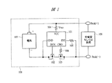
図1は本発明の一実施の形態による電池監視半導体装置の全体構成を示す図、図2(a),(b)は充電器の接続状態を示す図、図3は本実施の形態の電池監視半導体装置において、内部構成を示すブロック図、図4は図3の逆接続検出回路の構成例を示す回路図、図5は図3の逆接続検出回路の他の構成例を示す回路図である。 FIG. 1 is a diagram showing an overall configuration of a battery monitoring semiconductor device according to an embodiment of the present invention, FIGS. 2A and 2B are diagrams showing a connection state of a charger, and FIG. 3 is a battery according to the present embodiment. FIG. 4 is a block diagram showing an internal configuration of the monitoring semiconductor device, FIG. 4 is a circuit diagram showing a configuration example of the reverse connection detection circuit of FIG. 3, and FIG. 5 is a circuit diagram showing another configuration example of the reverse connection detection circuit of FIG. is there.
まず、図1により、本実施の形態による電池監視半導体装置の構成の一例を説明する。本実施の形態の電池監視半導体装置は、例えば電池監視IC101とされ、付加回路としてFET(Field Effect Transistor:電界効果型トランジスタ)102,103、抵抗104,105,106などからなり、電池107とともに電池パック108を構成している。
First, an example of the configuration of the battery monitoring semiconductor device according to the present embodiment will be described with reference to FIG. The battery monitoring semiconductor device according to the present embodiment is, for example, a
電池107の正(+)極は、電池パック108のPack(+)端子に接続され、また、抵抗104を介して電池監視IC101のVCC端子に接続される。
The positive (+) electrode of the
電池107の負(−)極は、FET102のソース電極と電池監視IC101のGND端子に接続される。
The negative (−) electrode of the
FET102のドレイン電極はFET103のドレイン電極に接続され、FET102のゲート電極は電池監視IC101のDCH端子に接続される。
The drain electrode of the
FET103のソース電極は電池パック108のPack(−)端子に接続され、また、抵抗105を介して電池監視IC101のIDT端子に接続され、FET103のゲート電極は抵抗106を介して電池監視IC101のCHG端子に接続される。
The source electrode of the FET 103 is connected to the Pack (−) terminal of the
電池パック108のPack(+)端子とPack(−)端子の間には、充電器もしくは負荷109が接続される。
A charger or a
電池監視IC101のVCC端子は正極側の電源端子、GND端子は負極側の電源端子である。 The VCC terminal of the battery monitoring IC 101 is a positive power supply terminal, and the GND terminal is a negative power supply terminal.
IDT端子(検出端子)は、過電流電圧検出入力、充電過電流検出入力及びCHG出力の負(−)極側電源端子であり、放電電流が増加してIDT端子の入力電圧が過電流検出電圧(V5)、または短絡電流検知電圧(V6)を超えるとDCH出力がロウレベル(GND)になり、その後、入力電圧がV5以下になると過電流状態から復帰する。過電流検出はGND電位に対するIDT端子電位を監視することによって行われる。 The IDT terminal (detection terminal) is an overcurrent voltage detection input, a charge overcurrent detection input, and a negative (−) pole side power supply terminal of the CHG output. The discharge current increases and the input voltage of the IDT terminal becomes the overcurrent detection voltage. When (V5) or the short-circuit current detection voltage (V6) is exceeded, the DCH output becomes low level (GND), and then, when the input voltage becomes V5 or less, the overcurrent state is restored. Overcurrent detection is performed by monitoring the IDT terminal potential with respect to the GND potential.
DCH端子は、放電回路遮断用外付けFET102の駆動信号出力であり、電池107の電圧が正常な時はハイレベル(VCC)となり、過放電状態または過電流状態を検出するとロウレベル(GND)になる。
The DCH terminal is a drive signal output of the
CHG端子は、充電回路遮断用外付けFET103の駆動信号出力であり、電池107の電圧が正常な時はハイレベル(VCC)となり、過充電状態または過大な充電器電圧を検出するとロウレベル(IDT)になる。
The CHG terminal is a drive signal output of the
図2に、充電器201の接続状態を示す。充電器201はPack(+)端子とPack(−)端子との間に接続され、図2(a)は正常接続状態である。図2(b)は充電器逆接続状態で、正負を逆に接続しているので異常電流が流れることになる。従来は、過電流検出機能によって異常電流を検出することにより間接的に逆接続を検出し、ノイズ除去タイマ時間後、FET102,103のゲート電位をコントロールすることにより電流遮断していた。本実施の形態では、IDT端子の電位が電源電圧VCCよりも高い電位の逆接続検出回路301(図3〜図5により後述)を設けることにより、充電器逆接続の異常状態を直接、IDT端子電圧で検出し、直ちに電流遮断を行う。すなわち、電源電圧よりも高い電位に検出電位を設け、異常状態を検知する。
FIG. 2 shows a connection state of the
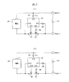
次に、図3により、電池監視IC101の内部構成の一例を説明する。本実施の形態による電池監視IC101は、例えば、逆接続検出回路301、制御回路302、駆動回路303、基準電圧発生回路304、上限電圧検出回路305、下限電圧検出回路306、発振器307、カウンタ308、充電器電圧検出回路309、放電電流検出回路310などから構成される。
Next, an example of the internal configuration of the battery monitoring IC 101 will be described with reference to FIG. The
逆接続検出回路301では、IDT端子からIDT311が入力し、駆動回路303へ検出信号312が出力している。また、検出信号312は、駆動回路303を介してCHG端子又はDCH端子に接続される。逆接続検出回路301は、IDT311の電位が電源電圧VCCよりも高い電位になると、充電器逆接続の異常状態を検出し、検出信号312が反転する。駆動回路303は、検出信号312の反転を受けて、充電回路遮断用素子駆動信号又は放電回路遮断用素子駆動信号を反転させて、直ちに電流遮断を行う。
In the reverse
次に、図4により、逆接続検出回路301の内部構成の一例を説明する。本実施の形態による逆接続検出回路301は、例えば、アノードがIDT(検出端子)311に接続されたダイオード401と、一方の端子がダイオード401のカソードに接続され、他方の端子が第1の電源GNDに接続された抵抗(R)402と、一方の入力がダイオード401のカソードに接続され、他方の入力が第2の電源(電源電圧)VCCに接続され、検出信号312を出力する比較器403と、などからなる。
Next, an example of the internal configuration of the reverse
この逆接続検出回路301では、ダイオード401の閾値電圧をVthとすると、IDT311の電位がVCC+Vth以上になった時、比較器403の出力(検出信号312)が反転して、充電器逆接続の異常を検出する。
In this reverse
図5に、逆接続検出回路301の内部構成の他の一例を示す。この例による逆接続検出回路301は、一方の端子がIDT(検出端子)311に接続された第1の抵抗(R1)501と、一方の端子が第1の抵抗501の他方の端子506に接続され、他方の端子が第1の電源GNDに接続された第2の抵抗(R2)502と、一方の端子が第2の電源(電源電圧)VCCに接続された第3の抵抗(R3)503と、一方の端子が第3の抵抗503の他方の端子507に接続され、他方の端子が第1の電源GNDに接続された第4の抵抗(R4)504と、一方の入力が第1の抵抗501の他方の端子506に接続され、他方の入力が第3の抵抗503の他方の端子507に接続され、検出信号312を出力する比較器505と、などからなる。R1,R2,R3,R4の各抵抗値は、[IDTの電位]>[VCCの電位]の条件で比較器505の出力(検出信号312)が反転するように設定する。これにより、IDT311の電位がVCCを超えた時、比較器403の出力(検出信号312)が反転して、充電器逆接続の異常を検出する。
FIG. 5 shows another example of the internal configuration of the reverse
したがって、本実施の形態の電池監視半導体装置によれば、電源電圧よりも高い電位に検出電位を設けた検出回路により充電器逆接続状態を検出し、直ちに電流を遮断して、より安全を向上させることができる。 Therefore, according to the battery monitoring semiconductor device of the present embodiment, the reverse connection state of the charger is detected by the detection circuit having the detection potential higher than the power supply voltage, and the current is immediately cut off, thereby improving safety. Can be made.
以上、本発明者によってなされた発明をその実施の形態に基づき具体的に説明したが、本発明は前記実施の形態に限定されるものではなく、その要旨を逸脱しない範囲で種々変更可能であることはいうまでもない。 As mentioned above, the invention made by the present inventor has been specifically described based on the embodiment. However, the invention is not limited to the embodiment, and various modifications can be made without departing from the scope of the invention. Needless to say.
例えば、前記実施の形態においては、リチウムイオン二次電池について説明したが、これに限定されるものではなく、他の二次電池(繰返し充電可能な電池)についても適用可能である。 For example, in the above-described embodiment, the lithium ion secondary battery has been described. However, the present invention is not limited to this, and can be applied to other secondary batteries (rechargeable batteries).
本発明は、リチウムイオン二次電池監視IC、充電制御IC等について適用可能である。 The present invention is applicable to a lithium ion secondary battery monitoring IC, a charging control IC, and the like.
101 電池監視IC
102,103 FET
104,105,106,402,501,502,503,504 抵抗
107 電池
108 電池パック
109 充電器もしくは負荷
201 充電器
301 逆接続検出回路
302 制御回路
303 駆動回路
304 基準電圧発生回路
305 上限電圧検出回路
306 下限電圧検出回路
307 発振器
308 カウンタ
309 充電器電圧検出回路
310 放電電流検出回路
311 IDT
312 検出信号
401 ダイオード
403,505 比較器
101 Battery monitoring IC
102,103 FET
104, 105, 106, 402, 501, 502, 503, 504
312
Claims (5)
前記半導体装置は、前記電池の電極に接続される一対の電極端子と、検出端子と、放電回路遮断用外付け素子が接続される端子と、充電回路遮断用外付け素子が接続される端子と、充電器電圧検出回路と、放電電流検出回路と、制御回路と、駆動回路と、を備え、前記充電器電圧検出回路と前記放電電流検出回路とは前記検出端子における電圧変動または電流変動に応じた信号を前記制御回路に送り、前記制御回路は前記充電器電圧検出回路と前記放電電流検出回路とからの信号に応じて前記駆動回路を制御して前記外付け素子のそれぞれに制御信号を与えるように構成されてなり、
前記半導体装置は、さらに、前記検出端子を入力とし、検出信号を前記駆動回路に出力する逆接続検出回路を備えてなり、前記検出端子の電位が電源電圧の電位を超えた時に前記検出信号を反転させ、タイマ時間を持たせた制御を経ることなく充電器からの電流を直ちに遮断するように構成されてなることを特徴とするリチウムイオン二次電池監視用半導体装置。 A semiconductor device for battery monitoring incorporated in a lithium ion secondary battery,
The semiconductor device includes a pair of electrode terminals connected to the electrode of the battery, a detection terminal, a terminal to which an external element for interrupting a discharge circuit is connected, and a terminal to which an external element for interrupting a charging circuit is connected A charger voltage detection circuit, a discharge current detection circuit, a control circuit, and a drive circuit, wherein the charger voltage detection circuit and the discharge current detection circuit correspond to voltage fluctuation or current fluctuation at the detection terminal. The control circuit sends a control signal to each of the external elements by controlling the drive circuit in accordance with signals from the charger voltage detection circuit and the discharge current detection circuit. Configured as
The semiconductor device further includes a reverse connection detection circuit that receives the detection terminal and outputs a detection signal to the drive circuit, and outputs the detection signal when the potential of the detection terminal exceeds the potential of the power supply voltage. A semiconductor device for monitoring a lithium ion secondary battery, wherein the semiconductor device is configured to immediately cut off a current from a charger without going through a control that is reversed and has a timer time.
前記逆接続検出回路は、
アノードが前記検出端子に接続されたダイオードと、
一方の端子が前記ダイオードのカソードに接続され、他方の端子が第1の電源に接続された抵抗と、
一方の入力が前記ダイオードのカソードに接続され、他方の入力が第2の電源に接続され、前記検出信号を出力する比較器と、を有することを特徴とするリチウムイオン二次電池監視用半導体装置。 In the lithium ion secondary battery monitoring semiconductor device according to claim 1,
The reverse connection detection circuit includes:
A diode having an anode connected to the detection terminal;
A resistor having one terminal connected to the cathode of the diode and the other terminal connected to a first power source;
A comparator for monitoring a lithium ion secondary battery, wherein one input is connected to the cathode of the diode, the other input is connected to a second power source, and the comparator outputs the detection signal. .
前記逆接続検出回路は、
一方の端子が前記検出端子に接続された第1の抵抗と、
一方の端子が前記第1の抵抗の他方の端子に接続され、他方の端子が第1の電源に接続された第2の抵抗と、
一方の端子が第2の電源に接続された第3の抵抗と、
一方の端子が前記第3の抵抗の他方の端子に接続され、他方の端子が前記第1の電源に接続された第4の抵抗と、
一方の入力が前記第1の抵抗の他方の端子に接続され、他方の入力が前記第3の抵抗の他方の端子に接続され、前記検出信号を出力する比較器と、を有することを特徴とするリチウムイオン二次電池監視用半導体装置。 In the lithium ion secondary battery monitoring semiconductor device according to claim 1,
The reverse connection detection circuit includes:
A first resistor having one terminal connected to the detection terminal;
A second resistor having one terminal connected to the other terminal of the first resistor and the other terminal connected to a first power source;
A third resistor having one terminal connected to a second power source;
A fourth resistor having one terminal connected to the other terminal of the third resistor and the other terminal connected to the first power source;
A comparator that has one input connected to the other terminal of the first resistor, the other input connected to the other terminal of the third resistor, and outputs the detection signal. A semiconductor device for monitoring lithium ion secondary batteries.
前記検出信号が反転した時に、直ちに、リチウムイオン二次電池と充電器との間の電流遮断を行う機能を有することを特徴とするリチウムイオン二次電池監視用半導体装置。 In the lithium ion secondary battery monitoring semiconductor device according to claim 1,
A semiconductor device for monitoring a lithium ion secondary battery, having a function of immediately interrupting a current between the lithium ion secondary battery and a charger when the detection signal is inverted.
前記検出信号が反転した時に、充電回路遮断用素子駆動信号又は放電回路遮断用素子駆動信号が反転する機能を有することを特徴とするリチウムイオン二次電池監視用半導体装置。 The semiconductor device for monitoring a lithium ion secondary battery according to claim 4,
Wherein when the detection signal is inverted, the lithium ion secondary battery monitoring semiconductor device and having a function of charging circuit interruption element driving signal or the discharge circuit interruption element drive signals are inverted.
Priority Applications (1)
| Application Number | Priority Date | Filing Date | Title |
|---|---|---|---|
| JP2005017569A JP4575179B2 (en) | 2005-01-26 | 2005-01-26 | Semiconductor device for monitoring lithium ion secondary batteries |
Applications Claiming Priority (1)
| Application Number | Priority Date | Filing Date | Title |
|---|---|---|---|
| JP2005017569A JP4575179B2 (en) | 2005-01-26 | 2005-01-26 | Semiconductor device for monitoring lithium ion secondary batteries |
Publications (3)
| Publication Number | Publication Date |
|---|---|
| JP2006210026A JP2006210026A (en) | 2006-08-10 |
| JP2006210026A5 JP2006210026A5 (en) | 2007-08-16 |
| JP4575179B2 true JP4575179B2 (en) | 2010-11-04 |
Family
ID=36966641
Family Applications (1)
| Application Number | Title | Priority Date | Filing Date |
|---|---|---|---|
| JP2005017569A Active JP4575179B2 (en) | 2005-01-26 | 2005-01-26 | Semiconductor device for monitoring lithium ion secondary batteries |
Country Status (1)
| Country | Link |
|---|---|
| JP (1) | JP4575179B2 (en) |
Cited By (1)
| Publication number | Priority date | Publication date | Assignee | Title |
|---|---|---|---|---|
| CN104467065A (en) * | 2013-09-24 | 2015-03-25 | 日立工机株式会社 | Charging device |
Families Citing this family (6)
| Publication number | Priority date | Publication date | Assignee | Title |
|---|---|---|---|---|
| JP5265934B2 (en) * | 2008-01-24 | 2013-08-14 | セイコーインスツル株式会社 | Charge / discharge control circuit |
| JP5032378B2 (en) * | 2008-03-31 | 2012-09-26 | セイコーインスツル株式会社 | Charge / discharge control circuit and battery device |
| KR101195716B1 (en) | 2008-03-31 | 2012-10-29 | 세이코 인스트루 가부시키가이샤 | Charge and discharge control circuit and battery device |
| JP5437770B2 (en) | 2009-10-20 | 2014-03-12 | セイコーインスツル株式会社 | Battery state monitoring circuit and battery device |
| JP6088289B2 (en) * | 2013-02-28 | 2017-03-01 | エスアイアイ・セミコンダクタ株式会社 | Charge / discharge control circuit and battery device |
| JP2019079662A (en) * | 2017-10-24 | 2019-05-23 | トヨタ自動車株式会社 | Initial charging method of secondary battery |
Citations (6)
| Publication number | Priority date | Publication date | Assignee | Title |
|---|---|---|---|---|
| JPH0191625A (en) * | 1987-09-30 | 1989-04-11 | Shindengen Electric Mfg Co Ltd | Charge and discharge circuit of battery |
| JPH07184318A (en) * | 1993-05-26 | 1995-07-21 | Siliconix Inc | Protective circuit for inversely connected battery |
| JP2001337125A (en) * | 2000-05-26 | 2001-12-07 | Aitekku:Kk | Tester for serial connection type battery |
| JP2002191130A (en) * | 2000-12-19 | 2002-07-05 | Nec Tokin Tochigi Ltd | Reverse-charge preventing circuit |
| JP2004113000A (en) * | 1992-11-24 | 2004-04-08 | Seiko Instruments Inc | Charging/discharging control circuit and rechargeable type power supply apparatus |
| JP2004242441A (en) * | 2003-02-06 | 2004-08-26 | Iwatsu Electric Co Ltd | Charger for secondary battery |
-
2005
- 2005-01-26 JP JP2005017569A patent/JP4575179B2/en active Active
Patent Citations (6)
| Publication number | Priority date | Publication date | Assignee | Title |
|---|---|---|---|---|
| JPH0191625A (en) * | 1987-09-30 | 1989-04-11 | Shindengen Electric Mfg Co Ltd | Charge and discharge circuit of battery |
| JP2004113000A (en) * | 1992-11-24 | 2004-04-08 | Seiko Instruments Inc | Charging/discharging control circuit and rechargeable type power supply apparatus |
| JPH07184318A (en) * | 1993-05-26 | 1995-07-21 | Siliconix Inc | Protective circuit for inversely connected battery |
| JP2001337125A (en) * | 2000-05-26 | 2001-12-07 | Aitekku:Kk | Tester for serial connection type battery |
| JP2002191130A (en) * | 2000-12-19 | 2002-07-05 | Nec Tokin Tochigi Ltd | Reverse-charge preventing circuit |
| JP2004242441A (en) * | 2003-02-06 | 2004-08-26 | Iwatsu Electric Co Ltd | Charger for secondary battery |
Cited By (1)
| Publication number | Priority date | Publication date | Assignee | Title |
|---|---|---|---|---|
| CN104467065A (en) * | 2013-09-24 | 2015-03-25 | 日立工机株式会社 | Charging device |
Also Published As
| Publication number | Publication date |
|---|---|
| JP2006210026A (en) | 2006-08-10 |
Similar Documents
| Publication | Publication Date | Title |
|---|---|---|
| KR100943576B1 (en) | Battery pack | |
| JP5061935B2 (en) | Battery pack | |
| JP4186052B2 (en) | Battery pack with charge control function | |
| US10116148B2 (en) | Secondary-battery protecting integrated circuit, secondary battery protection apparatus, and battery pack | |
| KR100993236B1 (en) | Back-gate voltage generator circuit, four-terminal back gate switching fet, and charge and discharge protection circuit using same | |
| KR101156345B1 (en) | Built-in charge circuit for secondary battery and secondary battery with the built-in charge circuit | |
| JP4575179B2 (en) | Semiconductor device for monitoring lithium ion secondary batteries | |
| TWI625910B (en) | Protection circuit and battery pack of lithium ion secondary battery | |
| JP2009060734A (en) | Charging circuit, battery pack with the same, and charging system | |
| JP2006320048A (en) | Protection circuit | |
| JP5742593B2 (en) | Semiconductor integrated circuit, protection circuit and battery pack | |
| TW201611467A (en) | Charge and discharge control circuit and battery device | |
| JP2009273305A (en) | Power supply and power supply for vehicle | |
| US8378635B2 (en) | Semiconductor device and rechargeable power supply unit | |
| US20160094068A1 (en) | Secondary battery protection circuit and battery device | |
| JP2005168159A (en) | Overcurrent protection circuit and charging type battery pack | |
| JP5338047B2 (en) | Battery pack | |
| JP2006210026A5 (en) | ||
| KR20180047178A (en) | Battery protection circuit for common use of csr supporting ic | |
| JP2009104821A (en) | Battery pack | |
| JP2011239652A (en) | Battery protection device and integrated circuit for battery protection | |
| JP5177842B2 (en) | Protection circuit and battery pack | |
| JPH0433271A (en) | Charging type battery device | |
| KR101892950B1 (en) | Battery protection circuit and battery protection apparatus and battery pack | |
| JP2005168160A (en) | Overcurrent protection circuit and charging type battery pack |
Legal Events
| Date | Code | Title | Description |
|---|---|---|---|
| A521 | Request for written amendment filed |
Free format text: JAPANESE INTERMEDIATE CODE: A523 Effective date: 20070703 |
|
| A621 | Written request for application examination |
Free format text: JAPANESE INTERMEDIATE CODE: A621 Effective date: 20070703 |
|
| A977 | Report on retrieval |
Free format text: JAPANESE INTERMEDIATE CODE: A971007 Effective date: 20100430 |
|
| A131 | Notification of reasons for refusal |
Free format text: JAPANESE INTERMEDIATE CODE: A131 Effective date: 20100511 |
|
| A521 | Request for written amendment filed |
Free format text: JAPANESE INTERMEDIATE CODE: A523 Effective date: 20100618 |
|
| TRDD | Decision of grant or rejection written | ||
| A01 | Written decision to grant a patent or to grant a registration (utility model) |
Free format text: JAPANESE INTERMEDIATE CODE: A01 Effective date: 20100727 |
|
| A01 | Written decision to grant a patent or to grant a registration (utility model) |
Free format text: JAPANESE INTERMEDIATE CODE: A01 |
|
| A61 | First payment of annual fees (during grant procedure) |
Free format text: JAPANESE INTERMEDIATE CODE: A61 Effective date: 20100819 |
|
| R150 | Certificate of patent or registration of utility model |
Ref document number: 4575179 Country of ref document: JP Free format text: JAPANESE INTERMEDIATE CODE: R150 Free format text: JAPANESE INTERMEDIATE CODE: R150 |
|
| FPAY | Renewal fee payment (event date is renewal date of database) |
Free format text: PAYMENT UNTIL: 20130827 Year of fee payment: 3 |
|
| S531 | Written request for registration of change of domicile |
Free format text: JAPANESE INTERMEDIATE CODE: R313531 |
|
| R350 | Written notification of registration of transfer |
Free format text: JAPANESE INTERMEDIATE CODE: R350 |
|
| S111 | Request for change of ownership or part of ownership |
Free format text: JAPANESE INTERMEDIATE CODE: R313113 |
|
| R350 | Written notification of registration of transfer |
Free format text: JAPANESE INTERMEDIATE CODE: R350 |
|
| R250 | Receipt of annual fees |
Free format text: JAPANESE INTERMEDIATE CODE: R250 |