JP2010537275A - Touch screen using oriented micro linear conductive elements - Google Patents
Touch screen using oriented micro linear conductive elements Download PDFInfo
- Publication number
- JP2010537275A JP2010537275A JP2010521037A JP2010521037A JP2010537275A JP 2010537275 A JP2010537275 A JP 2010537275A JP 2010521037 A JP2010521037 A JP 2010521037A JP 2010521037 A JP2010521037 A JP 2010521037A JP 2010537275 A JP2010537275 A JP 2010537275A
- Authority
- JP
- Japan
- Prior art keywords
- polarization
- conductive material
- mlces
- substrate
- assembly
- Prior art date
- Legal status (The legal status is an assumption and is not a legal conclusion. Google has not performed a legal analysis and makes no representation as to the accuracy of the status listed.)
- Pending
Links
Images


Classifications
-
- G—PHYSICS
- G06—COMPUTING; CALCULATING OR COUNTING
- G06F—ELECTRIC DIGITAL DATA PROCESSING
- G06F3/00—Input arrangements for transferring data to be processed into a form capable of being handled by the computer; Output arrangements for transferring data from processing unit to output unit, e.g. interface arrangements
- G06F3/01—Input arrangements or combined input and output arrangements for interaction between user and computer
- G06F3/03—Arrangements for converting the position or the displacement of a member into a coded form
- G06F3/041—Digitisers, e.g. for touch screens or touch pads, characterised by the transducing means
- G06F3/044—Digitisers, e.g. for touch screens or touch pads, characterised by the transducing means by capacitive means
- G06F3/0444—Digitisers, e.g. for touch screens or touch pads, characterised by the transducing means by capacitive means using a single conductive element covering the whole sensing surface, e.g. by sensing the electrical current flowing at the corners
-
- G—PHYSICS
- G06—COMPUTING; CALCULATING OR COUNTING
- G06F—ELECTRIC DIGITAL DATA PROCESSING
- G06F3/00—Input arrangements for transferring data to be processed into a form capable of being handled by the computer; Output arrangements for transferring data from processing unit to output unit, e.g. interface arrangements
- G06F3/01—Input arrangements or combined input and output arrangements for interaction between user and computer
- G06F3/03—Arrangements for converting the position or the displacement of a member into a coded form
- G06F3/041—Digitisers, e.g. for touch screens or touch pads, characterised by the transducing means
- G06F3/044—Digitisers, e.g. for touch screens or touch pads, characterised by the transducing means by capacitive means
-
- G—PHYSICS
- G06—COMPUTING; CALCULATING OR COUNTING
- G06F—ELECTRIC DIGITAL DATA PROCESSING
- G06F3/00—Input arrangements for transferring data to be processed into a form capable of being handled by the computer; Output arrangements for transferring data from processing unit to output unit, e.g. interface arrangements
- G06F3/01—Input arrangements or combined input and output arrangements for interaction between user and computer
- G06F3/03—Arrangements for converting the position or the displacement of a member into a coded form
- G06F3/041—Digitisers, e.g. for touch screens or touch pads, characterised by the transducing means
- G06F3/045—Digitisers, e.g. for touch screens or touch pads, characterised by the transducing means using resistive elements, e.g. a single continuous surface or two parallel surfaces put in contact
-
- G—PHYSICS
- G06—COMPUTING; CALCULATING OR COUNTING
- G06F—ELECTRIC DIGITAL DATA PROCESSING
- G06F2203/00—Indexing scheme relating to G06F3/00 - G06F3/048
- G06F2203/041—Indexing scheme relating to G06F3/041 - G06F3/045
- G06F2203/04113—Peripheral electrode pattern in resistive digitisers, i.e. electrodes at the periphery of the resistive sheet are shaped in patterns enhancing linearity of induced field
-
- Y—GENERAL TAGGING OF NEW TECHNOLOGICAL DEVELOPMENTS; GENERAL TAGGING OF CROSS-SECTIONAL TECHNOLOGIES SPANNING OVER SEVERAL SECTIONS OF THE IPC; TECHNICAL SUBJECTS COVERED BY FORMER USPC CROSS-REFERENCE ART COLLECTIONS [XRACs] AND DIGESTS
- Y10—TECHNICAL SUBJECTS COVERED BY FORMER USPC
- Y10T—TECHNICAL SUBJECTS COVERED BY FORMER US CLASSIFICATION
- Y10T428/00—Stock material or miscellaneous articles
- Y10T428/249921—Web or sheet containing structurally defined element or component
- Y10T428/249924—Noninterengaged fiber-containing paper-free web or sheet which is not of specified porosity
- Y10T428/24994—Fiber embedded in or on the surface of a polymeric matrix
Landscapes
- Engineering & Computer Science (AREA)
- General Engineering & Computer Science (AREA)
- Theoretical Computer Science (AREA)
- Human Computer Interaction (AREA)
- Physics & Mathematics (AREA)
- General Physics & Mathematics (AREA)
- Position Input By Displaying (AREA)
- Laminated Bodies (AREA)
- Non-Insulated Conductors (AREA)
Abstract
カバーシートアセンブリ(10)をタッチスクリーンシステム(200)に提供する。カバーシートアセンブリは、タッチスクリーンシステムの基板の導電性領域にわたって配置するように構成した表面(14)を有する絶縁層(12)を含む。導電性材料(16)は、絶縁層表面の少なくとも一部に配置されている。導電性材料が、第1方向に対して垂直な第2方向に偏光した第2偏光に対してよりも、第1偏光に対して一層透明であるように、導電性材料は、第1偏光の第1方向に対して配向するパターンで配置した複数の微小直線状導電性要素(22)を含む。 A cover sheet assembly (10) is provided for the touch screen system (200). The cover sheet assembly includes an insulating layer (12) having a surface (14) configured to be disposed over a conductive region of a substrate of the touch screen system. The conductive material (16) is disposed on at least a part of the surface of the insulating layer. The conductive material is more transparent to the first polarization than to the second polarization polarized in the second direction perpendicular to the first direction so that the conductive material is more transparent to the first polarization. It includes a plurality of minute linear conductive elements (22) arranged in a pattern oriented with respect to the first direction.
Description
本発明の背景
本発明は、一般的にはコンピュータタッチスクリーンに関し、より詳細にはタッチスクリーン用導電性材料に関する。
BACKGROUND OF THE INVENTION The present invention relates generally to computer touch screens, and more particularly to conductive materials for touch screens.
1970年代初頭のそれらの導入以来、タッチスクリーンは、ある種のコンピュータ用途に対してキーボードの代替手段を提供してきた。タッチスクリーンが利用者にコンピュータへのアクセスを提供するため、多くの状況において、キーボードおよびマウスは省略されている。抵抗性タッチスクリーンおよび容量性タッチスクリーンは双方とも、例えば液晶ディスプレイ(LCD)といったディスプレイの面にわたって配置される、ガラスパネルのような基板を一般的に含む。基板は、その表面に導電性材料を含む。使用者のタッチスクリーンへの入力を受け取るために、導電性材料は基板表面に導電性領域を規定する。入力を選択するよう、使用者が触れる表面を提供するために、絶縁層が導電性領域にわたって配置されている。 Since their introduction in the early 1970s, touch screens have provided keyboard alternatives for certain computer applications. In many situations, the keyboard and mouse are omitted because the touch screen provides the user with access to the computer. Both resistive touch screens and capacitive touch screens typically include a substrate, such as a glass panel, that is disposed over the surface of a display, eg, a liquid crystal display (LCD). The substrate includes a conductive material on its surface. In order to receive input to the user's touch screen, the conductive material defines a conductive region on the substrate surface. An insulating layer is disposed over the conductive region to provide a surface that the user touches to select the input.
抵抗性タッチスクリーンにおいて、絶縁層は、基板と向かい合う絶縁層の表面にわたって配置した第2導電性材料を含む、カバーシートの一部を形成する。2つの導電性材料が離間するように、複数の絶縁ドットが、カバーシートを基板から離間させている。使用者がカバーシートに触れると、2つの導電性材料は使用者が触れた箇所にて互いに係合する(engage)。容量性タッチスクリーンにおいて、絶縁層は、基板上の導電性材料に直接配置されている。 In a resistive touch screen, the insulating layer forms part of a cover sheet that includes a second conductive material disposed over the surface of the insulating layer facing the substrate. A plurality of insulating dots separate the cover sheet from the substrate so that the two conductive materials are separated. When the user touches the cover sheet, the two conductive materials engage each other where the user touches. In capacitive touch screens, the insulating layer is placed directly on the conductive material on the substrate.
基板および絶縁層の双方の上にある導電性材料を、一般的には酸化インジウムスズ(ITO)から作る。幾つかのタッチスクリーン用途に望ましいように、ITOは、導電率の所定値に対して良好な透明性を一般的に提供するため、ITOはしばしば用いられている。しかしながら、インジウムの供給は限られているため、ITOは比較的高価になり得る。更に、インジウムの需要を増加させることは、世界の供給量が減少するにつれて、ITOをより一層高価にさせる可能性がある。ITOを代替するために、導電性ポリマーの分子、カーボンナノチューブおよび/または金属ナノファイバのような、幾つかの種類の微小直線状導電性要素(MLCEs)が、タッチスクリーンの基板および/またはカバーシート上に存在する導電性材料中に用いるように提案されている。しかしながら、少なくとも幾つかのそのような提案されているMLCE材料は、所定の導電率に対して、ITOの透明性に及ばない。 The conductive material on both the substrate and the insulating layer is typically made from indium tin oxide (ITO). ITO is often used because ITO generally provides good transparency for a given value of conductivity, as is desirable for some touch screen applications. However, ITO can be relatively expensive due to the limited supply of indium. Furthermore, increasing the demand for indium can make ITO even more expensive as world supply decreases. To replace ITO, several types of micro-linear conductive elements (MLCEs), such as conductive polymer molecules, carbon nanotubes and / or metal nanofibers, are used for touch screen substrates and / or cover sheets. It has been proposed for use in the conductive material present above. However, at least some such proposed MLCE materials do not reach the transparency of ITO for a given conductivity.
導電性材料の所望の程度の導電率を維持しながら、タッチスクリーン用のMLCEに基づく導電性材料の透明性を向上させる必要がある。 There is a need to improve the transparency of MLCE based conductive materials for touch screens while maintaining the desired degree of conductivity of the conductive material.
本発明の簡単な説明
1つの実施態様において、カバーシートアセンブリをタッチスクリーンシステムに提供する。カバーシートアセンブリは、タッチスクリーンシステムの基板の導電性領域にわたって配置するように構成した表面を有する絶縁層を含む。導電性材料は、絶縁層表面の少なくとも一部に配置されている。導電性材料が、第1方向に対して垂直な第2方向に偏光した第2偏光に対してよりも、第1偏光に対して一層透明であるように、導電性材料は、第1偏光の第1方向に対して配向するパターンで配置した複数の微小直線状導電性要素を含む。
BRIEF DESCRIPTION OF THE INVENTION In one embodiment, a cover sheet assembly is provided for a touch screen system. The cover sheet assembly includes an insulating layer having a surface configured to be disposed over a conductive region of a substrate of the touch screen system. The conductive material is disposed on at least a part of the surface of the insulating layer. The conductive material is more transparent to the first polarization than to the second polarization polarized in the second direction perpendicular to the first direction so that the conductive material is more transparent to the first polarization. It includes a plurality of minute linear conductive elements arranged in a pattern oriented with respect to the first direction.
もう1つの実施態様において、基板アセンブリをタッチスクリーンシステムに提供する。基板アセンブリは、基板、および基板上に導電性タッチ領域を提供するために、基板の表面の少なくとも一部に配置した導電性材料を含む。導電性材料が、第1方向に対して垂直な第2方向に偏光した第2偏光に対してよりも、第1偏光に対して一層透明であるように、導電性材料は、第1偏光の第1方向に対して配向するパターンで配置した複数の微小直線状導電性要素を含む。 In another embodiment, a substrate assembly is provided for the touch screen system. The substrate assembly includes a substrate and a conductive material disposed on at least a portion of the surface of the substrate to provide a conductive touch area on the substrate. The conductive material is more transparent to the first polarization than to the second polarization polarized in the second direction perpendicular to the first direction so that the conductive material is more transparent to the first polarization. It includes a plurality of minute linear conductive elements arranged in a pattern oriented with respect to the first direction.
もう1つの実施態様において、タッチスクリーンシステム用の基板アセンブリを提供する。基板アセンブリは、第1表面および第1表面に対向する第2表面を有する基板、ならびに基板上に導電性タッチ領域を提供するために、基板の第1表面の少なくとも一部に配置した第1導電性材料を含む。第2導電性材料は、基板の第2表面の少なくとも一部に配置されている。第2導電性材料が、第1方向に対して垂直な第2方向に偏光した第2偏光に対してよりも、第1偏光に対して一層透明であるように、第2導電性材料は、第1偏光の第1方向に対して配向するパターンで配置した複数の微小直線状導電性要素を含む。 In another embodiment, a substrate assembly for a touch screen system is provided. The substrate assembly includes a substrate having a first surface and a second surface opposite the first surface, and a first conductive disposed on at least a portion of the first surface of the substrate to provide a conductive touch region on the substrate. Contains sexual materials. The second conductive material is disposed on at least a part of the second surface of the substrate. The second conductive material is such that the second conductive material is more transparent to the first polarization than to the second polarization polarized in a second direction perpendicular to the first direction. A plurality of minute linear conductive elements arranged in a pattern oriented with respect to the first direction of the first polarization.
発明の詳細な説明
本明細書で用いる場合、材料上に2つの地点が存在し、その間で約10メガオーム未満の抵抗を有するように測定され得る場合、その材料は導電性を有すると見なす。
Detailed Description of the Invention As used herein, a material is considered to be conductive if there are two points on the material that can be measured to have a resistance of less than about 10 megohms between them.
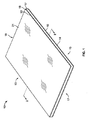
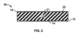
図1は、本発明の1つの実施態様に基づいて作った、タッチスクリーンカバーシートアセンブリ10の斜視図である。図2は、タッチスクリーンカバーシートアセンブリ10の断面図である。アセンブリ10を、抵抗性タッチスクリーンシステム(図1および図2に図示せず)と一緒に用いてよい。アセンブリ10を組み込んだ例示的なタッチスクリーンシステムを、以下でより詳細に説明する。アセンブリ10は、導電性材料16によって少なくとも部分的に被覆した表面14を有する絶縁層12を含む。以下でより詳細に説明するように、導電性材料は、複数の微小直線状導電性要素(MLCEs、図1および図2には図示せず)を含む。絶縁層12は、端部部分13、15、17および19の間で延在する。場合によっては、一般的にはカバーシートアセンブリ10および/または特に表面20の耐久性の向上を助けるために、絶縁層12は、表面14に対向する表面20にコーティング18を含んでもよい。コーティング18をいずれの適当な材料から作ってもよく、それは例えばアクリル樹脂および/またはガラスであるが、これらに限定されない。
FIG. 1 is a perspective view of a touch screen
図8について以下でより詳細に説明するように、使用に際して、表面14およびその上の導電性材料16が基板とほぼ向かい合うように、アセンブリ10は、タッチスクリーンシステムの基板(図1および図2には図示せず)上に保持されている。コーティング18の表面21、あるいはコーティング18を含まない場合、その代わりに表面20は、タッチスクリーンシステムが表示した入力を選択するために、使用者が触れることができる露出したタッチ表面を提供する。
As will be described in more detail below with respect to FIG. 8, in use, the
絶縁層12が本明細書で説明するように機能できるいずれの適当な材料から絶縁層12を作ってもよく、それは例えばポリエステル、ポリエチレンテレフタレート(PET)、ポリエチレンナフタレート(PEN)および/またはガラスであるが、これらに限定されない。例えば、アセンブリ10の特定の用途および/またはアセンブリ10を一緒に用いるタッチスクリーンの種類に応じて、絶縁層12は完全に透明または部分的に透明であってよい。幾つかの実施態様において、絶縁層12の1つまたはそれより多くの部分は、不透明であってよい。例えば、アセンブリ10の特定の用途ならびに/またはアセンブリ10を一緒に用いるタッチスクリーンシステムの種類および/もしくは構造に応じて、絶縁層12は、絶縁層12が本明細書で説明するように機能できるいずれの適当な寸法および/または形状を有してもよく、それは例えば矩形、円形、三角形および/または楕円形の形状であるが、これらに限定されない。
Insulating
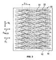
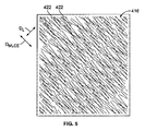
図3は、参照数字22で示される複数のMLCEsを図示する、カバーシートアセンブリ10の概略図である。図4は、MLCE22の例示的な実施態様の概略図である。明確にするために、MLCEs22の寸法は誇張されており、MLCEs22のパターンの密度も低くなるように、MLCEs22の数は減らされている。アセンブリ10を一緒に用いるディスプレイ(図示せず)に対して、導電性材料16が所定の透明性を有するように、MLCEs22を配置する。特に、タッチスクリーンと一緒に用いる幾つかのディスプレイ(図示せず)は、偏光を発する。例えば、幾つかの液晶ディスプレイ(LCDs)は、偏光した光を発することがよく知られている。より詳細には、LCDsは、一般的にはバックライト、バックライトと液晶材料との間に偏光フィルム、およびその液晶材料の反対側に第2偏光フィルムを含む。第2偏光フィルムに到達する光の偏光の向きに、液晶が及ぼす影響の結果として、LCDの各ディスプレイの画素は、電気的に制御される光バルブとして機能する。第2偏光フィルムを出る光は、直線偏光している。第2偏光フィルムの偏光軸の向きに応じて、LCDが発する光は、水平に偏光しても、垂直に偏光しても、45°の角度に偏光しても、またはいずれかの他の向きに偏光してもよい。水平に偏光した光は、関連する電場が水平方向に振動する光である。垂直に偏光した光は、関連する電場が垂直方向に振動する光である。45°の角度に偏光した光は、関連する電場が水平方向および垂直方向の双方に対して45°の角度を成す方向に振動する光である。所定の透明性を提供するために、MLCEs22は、ディスプレイが発する偏光に対してそれぞれ配向する。導電性材料16が、ディスプレイが発する偏光に部分的に透明または完全に透明であるように、MLCEs22は配向してよい。幾つかの実施態様において、導電性材料16の必ずしも全ての部分が、所定の透明性を有するわけではないことが望ましいことがあり、そのような部分において、MLCEs22は、所定の透明性を提供するようには配向していない。
FIG. 3 is a schematic view of the
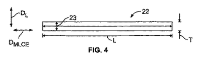
本明細書で用いる場合、MLCEs22を、電子が沿って動く導電性材料16内での線形パスとしてそれぞれ規定する。(本明細書で用いる場合、「電子」は、電子または半導体の概念における「正孔」のいずれかである電荷担体を略した表記である)。以下でより詳細に説明するように、MLCEs22は、限定するわけではないが、カーボンナノ粒子、金属ナノ粒子、導電性ポリマーの原子の分子鎖および/または同様のものであってよい。MLCEs22が導電性ポリマーの原子の分子鎖である実施態様において、MLCEs22は、電子が沿って動く分子鎖の線形パスである。MLCEs22がカーボンナノ粒子、金属ナノ粒子および/または同様のものである実施態様において、MLCEs22は、電子が沿って動く線形パスを形成する、ナノ粒子、金属ナノ粒子および/または同様のものの部分である。図4に示すように、場合によっては、幾らかまたは全部のMLCEs22は細長くてよく、そのMLCEs22各々は、それらの太さ(または厚さ)Tよりも実質的に大きい(かつ図4の例示的な実施態様において、太さTに等しいそれらの幅よりも実質的に大きい)長さLを有する。例えば、MLCEs22は、それらの太さT(および/もしくはそれらの幅)の3倍またはそれより多くの倍数である長さLを有してよい。場合によっては、長さLは、太さT(および/もしくはそれらの幅)の10倍またはそれより多くの倍数であってもよい。MLCEs22の細長い形状は、MLCEs22に異方性を有する導電特性を与える。例示的な実施態様において、MLCEs22の太さTおよび幅が同じであるようにして、MLCEs22は略円形の断面を有しているが、MLCEs22は、いずれの適当な断面形状をそれぞれ含んでもよい。例示的な実施態様において、MLCEs22の太さTおよび幅の寸法は、1ミクロンと等しいまたはそれより小さく、他方、MLCEs22の長さLは1ミクロンより大きい。しかしながら、幾つかの実施態様において、MLCEs22の太さTおよび/または幅の寸法は、1ミクロンより大きくてもよい。更に、MLCEs22の長さLは、1ミクロンより小さくてもよい。本明細書で用いる場合、「微小」なる用語および「ナノ」なる接頭語は、1ミクロン未満またはそれと等しい寸法、ならびに1ミクロンより大きい寸法を意味してもよい。
As used herein,
ディスプレイが発する光に対する所定の透明性を提供するために、MLCEs22は、ディスプレイが発する偏光に対してそれぞれ配向する。導電性材料16が、ディスプレイが発する光の偏光方向DLに対して垂直な方向D1に偏光した別の偏光に対してよりも、ディスプレイが発する偏光に対して一層透明であるように、例えばMLCEs22の長さLを、ディスプレイが発する光の電場の方向DLに対して配向するパターンで配置してよい。例えば、MLCEs22のパターンは、ディスプレイが発する光の偏光方向DLに対して垂直である、ディスプレイのものではない他の偏光の偏光方向D1とより整列した整列方向DMLCEに配向していてよい。導電性材料16が、ディスプレイが発する偏光に対する所定の透明性を提供するように、ディスプレイが発する光の電場の方向DLに対して配向する整列方向DMLCEの別の例は、絶縁層12の表面14に対して垂直な方向である。整列方向DMLCEが絶縁層表面14に対して垂直に延在するそのような実施態様において、整列方向DMLCEは、ディスプレイが発する光の偏光方向DLおよびディスプレイが発する光の偏光方向DLに対して垂直である、ディスプレイのものではない他の偏光の偏光方向D1の双方に対して垂直に延在し、従って、方向DLおよびD1の双方に偏光した光に対する所定の透明性を提供する。更に、偏光していない光を発するディスプレイにとって、光の横波特性は、方向DMLCEと双方とも垂直であるDL方向およびD1方向に偏光成分を更に制限し、従って、整列方向DMLCEが絶縁層表面14に対して垂直に延在する実施態様によって、偏光していない光を発するディスプレイに同じ透明性の利点が提供される。整列方向DMLCEが絶縁層表面14に対して垂直に延在するそのような実施態様において、導電層16の導電率は減少し得る。絶縁表面に対して垂直に延在する整列方向に配向するMLCEs22もあれば、絶縁層表面14と平行に延在する整列方向に配向するMLCEs22もある実施態様を用いることによって、導電率のそのような減少を、少なくとも部分的に埋め合わせてよい。
In order to provide a certain transparency to the light emitted by the display, the
幾つかの実施態様において、導電性材料16が、ディスプレイが発する偏光に対して垂直に偏光した光に対してよりも、ディスプレイが発する光に対して少なくとも1%一層透明であるように、MLCEs22のパターンは配向している。他の実施態様において、導電性材料16が、ディスプレイが発する偏光に対して垂直に偏光した光に対してよりも、ディスプレイが発する光に対して少なくとも2%一層透明であるように、MLCEs22のパターンは配向している。更に他の実施態様において、導電性材料16が、ディスプレイが発する偏光に対して垂直に偏光した光に対してよりも、ディスプレイが発する光に対して少なくとも5%一層透明であるように、MLCEs22のパターンは配向している。
In some embodiments, the
図1〜図4の例示的な態様において、MLCEs22のパターンが配向する整列方向DMLCEは、ディスプレイが発する光の偏光方向DLに対して垂直に偏光した、ディスプレイのものではない他の偏光の偏光方向D1とほぼ整列する。言い換えると、整列方向DMLCEは、ディスプレイが発する光の偏光方向DLに対して垂直にほぼ整列し、図1〜図4の実施形態において、方向DMLCEがほぼ水平であるように、それはほぼ垂直である。ディスプレイが発する偏光の電場は電子を励起し、それらの太さTに沿って(方向DLに沿って)MLCEs22内で移動させる。MLCEs22の太さTは、それらの長さLよりも実質的に小さい。電子をMLCEs22の長さLに沿って移動するように励起させる場合に限っては、電場によって励起させられる電子は動かない。MLCEs22の太さTに沿う例示的な電子の動き23を図4に図示する。従って、MLCEs22は、偏光していない光または方向DLに対して傾く方向に偏光した光(例えば、ディスプレイが発する光に対して垂直な偏光)よりも、ディスプレイが発する偏光とそれほど相互作用せず、従って、それほど散乱または吸収しない。
In the exemplary embodiment of FIGS. 1-4, the alignment direction D MLCE the pattern of MLCEs22 are aligned, the display is polarized perpendicular to the polarization direction D L of light emitted, other polarization do not display substantially aligned with the polarization direction D 1. In other words, the alignment direction D MLCE is substantially aligned perpendicular to the polarization direction D L of the light emitted by the display, in the embodiment of FIGS. 1-4, such that the direction DMLCE approximately a horizontal, it substantially vertical It is. Electric field polarization emitted by the display excites the electrons, along their thickness T (in the direction D L) is moved in the
必ずしも全てのMLCEs22の長さLが、整列方向DMLCEにほぼ配向しているわけでなくてもよい。図3に示すように、幾つかの態様においては、むしろ幾らかのMLCEs22の長さLは、整列方向DMLCEにほぼ配向しているわけではなく、むしろ方向DMLCEに対して傾いて配向している。しかしながら、図3の実施態様において、MLCEs22の配向の分布は、MLCEs22のパターンが、整列方向DMLCEに平均的な全体としての配向を有するようなものである。特に、ほぼ方向DMLCEに配向する長さLを有するMLCEs22の数、および方向DMLCEに対して傾き角度をなす各MLCEs22の角度は、導電性材料16のディスプレイが発する偏光に対する所定の透明性を提供するのに十分である。更に、MLCEs22が、導電性材料16内で導電性ネットワークを形成するために、MLCEs22は電気的に相互接続される必要がある。従って、MLCEs22はそれらの長さLに沿って実質的に真っ直ぐであることから偏奇してよく、(図3に示すように)MLCEs22は互いに重なってよく、および/またはMLCEs22は、MLCEs22を電気的に相互接続させるのに十分な導電率を有する、(限定するわけではないが、導電性ポリマーのような)マトリックス材料内に分散していてもおよび/または含有されていてよい。幾つかの他の実施形態において、例えば、限定するわけではないが、整列方向DMLCEが絶縁層12の表面に対してほぼ垂直に延在する実施形態、および/または所望の配向にMLCEs22を配置するために、(以下に記載する)テンプレートを用いる場合、全てのMLCEs22の長さLが整列方向DMLCEにほぼ配向していてよい。
The length L of all
導電性材料16のディスプレイが発する偏光に対する所定の透明性を提供できるほど、ディスプレイが発する偏光の電場によって引き起こされる電子の動きが小さくなるように、MLCEs22の太さを選択してよい。ディスプレイが発する偏光に対する所定の透明性を提供するMLCEs22の太さTのいずれの適当な値を選択してもよく、それは例えば、およそ分子の寸法から、ディスプレイが発する偏光の波長よりも小さい範囲のおよそ何百ナノメートルかの間であるが、これに限定されない。
The thickness of
図3に示すMLCEs22のパターンの例示的な配向は、ディスプレイが発する偏光に対する所定の透明性を提供することに加え、周辺光の反射の吸収を促すことができる。特に、方向DMLCEにほぼ平行な方向に偏光した周辺光の一部は電子を励起させ、MLCEs22の長さLに沿って移動させる。MLCEs22の太さTおよび長さLに沿う例示的な電子の動き23を図4に図示する。MLCEs22の太さ(または厚さ)Tに沿う動きと比べて、長さLに沿う電子のより大きな動きは、MLCEs22に方向DMLCEとほぼ平行に偏光した周辺光を吸収させる。従って、導電性材料16は、周辺光の一部が絶縁層12を通って進むことを阻止するよう促すことができる。そのようにして、例えば、ディスプレイの表面から反射する周辺光を抑えることにより、ディスプレイのコントラスト比を高めることを促す「減光フィルタ」として、導電性材料16を用いることができる。
The exemplary orientation of the pattern of
MLCEs22を含む導電性材料16を、導電性材料16が本明細書で説明するように機能できるいずれの適当な材料から作ってもよく、それは例えばカーボンナノ粒子、金属ナノ粒子および/または導電性ポリマーであるが、これらに限定されない。カーボンナノ粒子には、カーボンナノ粒子が本明細書で説明するように機能できるいずれの適当な形状、特性、構造および/または同様のものが含まれてもよく、それは例えばカーボンナノチューブ、カーボンナノファイバ、カーボンナノスフィアおよび/またはカーボンナノワイヤであるが、これらに限定されない。本明細書で用いる場合、「カーボンナノチューブ」なる用語は、例えば、シリンダー状構造を有するフラーレンなど、炭素を含むナノチューブを意味する。本明細書で説明する金属ナノ粒子を、いずれの適当な金属から作ってもよく、それは例えば銀、ビスマス、金、ニッケル、スズ、銅、亜鉛および/またはいずれかの他の導電性金属であるが、これらに限定されない。金属ナノ粒子には、金属ナノ粒子が本明細書で説明するように機能できるいずれの適当な形状、特性、構造および/または同様のものが含まれてもよく、それは例えば金属ナノファイバ、金属ナノスフィア、金属ナノチューブおよび/または金属ナノワイヤであるが、これらに限定されない。適当な導電性ポリマーの例には、チオフェン誘導体ポリマーおよび/またはポリチオフェン誘導体ポリマーが含まれるが、これらに限定されない。先に説明したように、導電性材料16をカーボンナノ粒子および/または金属ナノ粒子から少なくとも部分的に作った実施態様において、その金属ナノ粒子はMLCEs22である。先にも説明したように、導電性材料16を導電性ポリマーから少なくとも部分的に作った実施態様において、MLCEs22は、ポリマーの(限定するわけではないが、炭素原子のような)原子の分子鎖である。導電性材料16は、ナノ粒子および/または原子の分子鎖が本明細書で説明するように配向して機能できる、カーボンナノ粒子、金属ナノ粒子および/または導電性ポリマーを含む、いずれの適当な構造を有してもよい。導電性材料16を構築するのに適当であり得るカーボンナノ粒子および/または金属ナノ粒子を含む構造の例には、所望の配向に配置した複数のナノ粒子から少なくとも部分的に成る層、フィルムおよび/または布帛が含まれるが、これらに限定されない。導電性材料16を、ナノ粒子および/もしくは原子の分子鎖の単層である、カーボンナノ粒子、金属ナノ粒子および/もしくは原子の分子鎖の布帛、層ならびに/またはフィルムから構築してよく、あるいは場合によっては、カーボンナノ粒子、金属ナノ粒子および/または原子の分子鎖の複数の層から構築してもよい。幾つかの実施形態において、カーボンナノ粒子および/または金属ナノ粒子は、導電性材料16が本明細書で説明するように機能できる、1つもしくはそれより多くの他の適当な材料に分散していてもおよび/または含有されていてよく、それは例えば透明なポリマーおよび/または透明なセラミックであるが、これらに限定されない。マトリックスに適当なポリマーの例には、ポリメチルメタクリレート(PMMA)ポリアクリレート、ポリアクリロニトリル、ポリビニルアルコール、ポリエステル、ポリカーボネート、ポリウレタン、ポリビニルクロライドおよび/または溶媒に可溶ないずれかの他のポリマーが含まれるが、これらに限定されない。適当な溶媒の例には、トルエン、キシレン、メチルエチルケトン(MEK)および/または同様のものが含まれるが、これらに限定されない。
The
カーボンナノ粒子に関して、適当に制御した方向、長さおよび同様のものを有する個々のナノ粒子を成長させるまたは配置するために、カーボンナノ粒子の直接成長および/または化学的な自己集積化を用いてよい。カーボンナノ粒子に関して、導電性材料16には、単層カーボンナノチューブおよび/または多層カーボンナノチューブが含まれてよい。更に、カーボンナノチューブは、元の状態であっても、限定するわけではないが、金属のような別の材料によって機能化および/または充填され、カーボンナノチューブの内腔内に封入された「ナノワイヤ」を形成してもよい。
With respect to carbon nanoparticles, direct growth and / or chemical self-assembly of carbon nanoparticles is used to grow or position individual nanoparticles having appropriately controlled orientation, length and the like. Good. With respect to carbon nanoparticles, the
適用できる場合、導電性材料16を絶縁層表面14上で直接成長させて、またはその表面に配置してよく、あるいは表面14であらかじめ作り配置してよい。導電性材料16が本明細書で説明するように機能できるいずれの適当な方法、プロセス、構造ならびに/または手段を用いて、導電性材料16を絶縁層表面14に適用してもよく、それは例えばスピンコーティング、浸漬、噴霧(例えば、限定するわけではないが、エアロゾル塗布など)、スクリーン印刷操作、ならびに/または表面14上での直接成長(例えば、限定するわけではないが、スピンコートした触媒に基づく成長および/もしくは気相触媒の補助による化学蒸着(CVD)など)であるが、これらに限定されない。例えば、限定するわけではないが、スピンコーティング、噴霧、浸漬および/またはスクリーン印刷方法など、幾つかの配置方法において、導電性ポリマー原子、カーボンナノ粒子および/または金属ナノ粒子を、可溶性または不溶性の形態で適当な溶媒に分散および/または含有させてよい。表面14へのそのような例示的な種類の適用を制御するためのパラメータには、下部表面の表面機能化、スピンコーティングパラメータ(例えば、限定するわけではないが、長さ、MLCE懸濁濃度、スピンコーティング溶液濃度および/もしくは1分間あたりの回転数(RPM))、適用の回数、温度、pH、時間、触媒密度/濃度ならびに/または成長環境(限定するわけではないが、例えば成長時間、成長温度、および/もしくは気体濃度)が含まれる。MLCEs22がカーボンナノ粒子を含む場合、ナノ粒子間の内側接着性の向上を助けるために、場合によっては、(限定するわけではないが、例えば、カーボンナノ粒子にグラフトしたカルボキシル基を用いて、カーボンナノ粒子にグラフトしたジスルフィド基を用いて、カーボンナノ粒子にグラフトしたチオフェン基を用いて、および/または限定するわけではないがピレンのような平面共役炭化水素を用いて)、カーボンナノ粒子を機能化してもよい。本明細書で説明する幾つかの適用の間、カーボンナノ粒子は「自己組織化」特性を示してよく、そこでは個々のナノチューブは、エネルギー的に好ましい時はいつでも、適用される表面に接着する傾向がある。例えば、アセンブリ10の特定の用途および/またはアセンブリ10を一緒に用いるタッチスクリーンシステムの種類に応じて、個々のカーボンナノ粒子は、ファンデルワールス力の結果として互いに接着してよい。
Where applicable, the
MLCEs22を、いずれの適当な方法、プロセス、構造および/または手段を用いて所望の配向に配置してもよく、それは例えば流量調節、スクリーン印刷、電場効果、MLCEs22を少なくとも部分的に受容する寸法および形状の溝を含むテンプレート、および/または自己整列する特性の利用であるが、これらに限定されない。別の実施例は、最初にMLCEs22の不規則に配向したネットワークを形成し、次に、望ましくない配向を有するMLCEs22を、限定するわけではないが、偏光した赤外線および/または高周波(RF)加熱を用いるなどして除去および/または破壊することを含む。更なる別の実施例は、MLCEs22を所望の配向パターンで、限定するわけではないが、成長させるおよび/または配置するなどして形成すること、ならびに限定するわけではないが、先に記載したポリマーマトリックスのようなマトリックス内にMLCEs22の少なくとも一部を分散および/または含有させることによって、MLCEs22のそれぞれの位置を固定することを含む。
The
導電性材料16は、導電性材料16が本明細書で説明するように機能できるいずれかの適当な厚さで、表面14を被覆していてよい。場合によっては、一定の、限定するわけではないが抵抗のような導電特性を提供するために、導電性材料16が、表面14を均一な厚さで被覆する。幾つかの実施態様において、導電性材料16の厚さを、MLCEs22の長さによって規定してよい。他の実施態様において、導電性材料16の厚さは、層がMLCEs22の1層のみを含む場合、MLCEs22の1つの幅、太さおよび/または直径によって規定されてよく、あるいは導電性材料16がMLCEs22の1つより多くの層を含む場合、MLCEs22の複数の幅、太さおよび/または直径によって規定されてよい。導電性材料16が本明細書で説明するように機能できるいずれかの適当な抵抗を提供するために、導電性材料16の、例えば材料および/または厚さを選択してよく、それは例えば、約100オーム/スクエア〜約1000オーム/スクエアの抵抗であるが、これに限定されない。選択する抵抗を、例えばアセンブリ10の特定の用途および/またはアセンブリ10を一緒に用いるタッチスクリーンシステムの種類に応じて決めてよい。
The
図3および図4では、ディスプレイが発する偏光の電場の方向DLがほぼ垂直であるように示されているが、方向DLは、(図3および図4に示すように)ほぼ垂直に限定されない。むしろ、ディスプレイが発する光は、いずれの方向DLに偏光してもよい(および整列方向DMLCEを、所定の透明性を提供する、方向DLに対するいずれの方向として選択してもよい)。例えば、別の態様において、方向DLは、(図6に示すように)ほぼ水平であってもよい。方向DLは、ほぼ水平およびほぼ垂直以外の他の方向であってもよい。例えば、図5は、ディスプレイが発する光の偏光方向DLが、水平および垂直に対してほぼ45°に延在する実施態様を図示する。図5の例示的な実施態様において、導電性材料416の複数のMLCEs22のパターンの整列方向DMLCEは、ディスプレイが発する偏光の方向DLに対してほぼ垂直である。
In FIGS. 3 and 4, the direction D L of the polarized electric field emitted by the display is shown to be substantially vertical, but the direction D L is limited to being substantially vertical (as shown in FIGS. 3 and 4). Not. Rather, the light emitted by the display may be polarized in any direction D L (and the alignment direction D MLCE may be selected as any direction relative to the direction D L that provides a certain transparency). For example, in another aspect, the direction D L may be substantially horizontal (as shown in FIG. 6). Direction D L may be substantially horizontal and substantially another direction other than vertical. For example, FIG. 5, the polarization direction D L of the light emitted by the display is illustrated an embodiment thereof extending in a substantially 45 ° to the horizontal and vertical. In the exemplary embodiment of FIG. 5, the alignment direction D MLCE of the pattern of the plurality of
導電性材料416およびMLCEs422は、導電性材料16(図1〜図3)およびMLCEs22とそれぞれ実質的に同様である。従って、導電性材料16およびMLCEs22の説明および図示を、導電性材料416およびMLCEs422に適用できる。例えば、導電性材料416の構成、材料構築、構造物の太さ(または厚さ)、電気特性、機械特性、利点、適用方法および/または手段ならびに同様のもの、ならびにMLCEs22の利点、構成、配置、構造、材料構築配向、寸法、形状および同様のものは、導電性材料16およびMLCEs22のそれとそれぞれ実質的に同様である。従って、導電性材料416およびMLCEs422を本明細書で更に詳細には説明しない。
図6は、本発明の1つの態様に基づいて形成したタッチスクリーン基板アセンブリ110の上面図である。図7は、図6の線7−7に沿って得られるアセンブリ110の断面図である。アセンブリ110を、例えば、抵抗性または容量性タッチスクリーンシステムなど、いずれの適当なタッチスクリーンシステム(図6および図7に図示せず)と一緒に用いてもよい。アセンブリ110を組み込んだ例示的なタッチスクリーンシステムを、以下でより詳細に説明する。アセンブリ110は、導電性材料116によって少なくとも部分的に被覆した表面114を有する基板112を含む。表面114を被覆する導電性材料116は、表面114に導電性タッチ領域118を提供する。アセンブリ110は、タッチ領域118を縁取る、導電性材料116上の導電性電極120のパターンによって形成された、抵抗のネットワークを含む。
FIG. 6 is a top view of a touch
導電性材料116は、詳細Aに図示する複数のMLCEs122を含む。明確にするために、MLCEs122の寸法および間隔は誇張されていてよく、かつMLCEs122のパターン全体の密度も減少するように、MLCEs122の数は減らされていてよい。MLCEs22(図3および図4)を有する場合、導電性材料116が、アセンブリ110を一緒に用いるディスプレイ(図示せず)に対して所定の透明性を有するように、MLCEs122を配置する。例示的な態様において、MLCEs122のパターン全体が、方向DLに対してほぼ垂直な方向DMLCEに配向するように配置されており、導電性材料116は、ディスプレイが発する偏光にほぼ完全に透明であるように、MLCEs122は配置されている。
The
導電性材料116およびMLCEs122は、導電性材料16(図1〜図3)およびMLCEs22とそれぞれ実質的に同様である。従って、導電性材料16およびMLCEs22の説明および図示は、導電性材料116およびMLCEs122にそれぞれ適用できる。例えば、導電性材料116の構成、材料構築、構造物の太さ、電気特性、機械特性、利点、適用方法および/または手段ならびに同様のもの、ならびにMLCEs122の利点、構成、配置、構造、材料構築配向、寸法、形状および同様のものは、導電性材料16およびMLCEs22とそれぞれ実質的に同じである。従って、導電性材料116およびMLCEs122を本明細書で更に詳細には説明しない。しかしながら、使用者が触れた時、導電性材料16と異なり、導電性材料116は曲げられていないことを意味してよく、従って、幾つかの実施態様において、導電性材料116はよりもろい構築物によって作られてよい。
導電性材料116のMLCEs122の異方特性は、アセンブリ110を含むタッチスクリーンシステムの動作に影響を及ぼし得る。例えば、MLCEs122の異方特性は、使用者が触った時、タッチ領域18の座標測定に間違いまたは変化をもたらし得る。そのような間違いまたは変化は、例えば、タッチスクリーンシステムの較正の間に決定される補正係数を用いて、補正される必要があり得る。
The anisotropic properties of the
例示的な実施態様において、電極120は導電性材料116に直接配置されている。別の実施態様において、電極120は、導電性材料116の下部で基板表面114に直接配置されている。電極120のパターンは、ほんの例示的なものを意味しており、従って、電極120は、図6に示すパターンに限定されない。むしろ電極120は、タッチスクリーン基板アセンブリ110が本明細書で説明するように機能できるいずれの適当なパターンを有してもよい。同様に、電極120は、例えば、アセンブリ110の特定の用途および/もしくはアセンブリ110を一緒に用いるタッチスクリーンシステムの種類によって決めることができる、いずれの適当な寸法、形状、抵抗、導電率を有してもよく、ならびに/またはいずれの適当な材料(例えば、限定するわけではないが、銀のフリットおよび/もしくはMLCEs122の密度がより高い導電性材料116の材料など)から作ってもよい。例えば、アセンブリ110の特定の用途および/またはアセンブリ110を一緒に用いるタッチスクリーンシステムの種類に応じて、電極120は完全に透明、部分的に透明、または不透明であってよい。アセンブリ110において、既知のタッチスクリーン基板のデザインの中で、導電性電極120と組み合わせて時々含まれる欠失ライン(deletion line)(図示せず)を形成するように、導電性材料116のある領域を除去してよい。
In the exemplary embodiment,
基板112を、基板112が本明細書で説明するように機能できるいずれの適当な材料から作ってもよく、それは例えばガラス、セラミック、および/またはプラスチックであるが、これらに限定されない。例えば、アセンブリ110の特定の用途および/またはアセンブリ110を一緒に用いるタッチスクリーンシステムの種類に応じて、基板112は完全に透明または部分的に透明であってよい。例えば、アセンブリ110の特定の用途ならびに/またはアセンブリ110を一緒に用いるタッチスクリーンシステムの種類および/もしくは構造に応じて、基板112は、絶縁層112が本明細書で説明するように機能できるいずれの適当な寸法および/または形状を有してもよく、それは例えば矩形、円形、三角形および/または楕円形の形状であるが、これらに限定されない。
The
例えば、アセンブリ110の特定の用途ならびに/またはアセンブリ110を一緒に用いるタッチスクリーンシステムの種類に応じて、タッチ領域118は、タッチ領域118が本明細書で説明するように機能できるいずれの適当な寸法および/または形状を有してもよく、それは例えば矩形、円形、三角形および/または楕円形の形状であるが、これらに限定されない。例示的な実施態様において、タッチ領域118は略矩形形状を有し、電極120によって縁取られる基板表面114の領域を覆う。
For example, depending on the particular application of
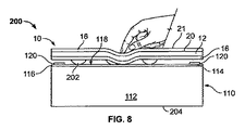
図8は、本明細書で説明および/もしくは図示するタッチスクリーン基板アセンブリの実施態様ならびに/またはカバーシートアセンブリの実施態様を含むことができる、抵抗性タッチスクリーンシステム200の断面図である。幾つかの実施態様において、抵抗性タッチスクリーンシステム200は4線式システムである。別の実施態様において、システム200は5線式システムであってよい。限定するわけではないが、LCDおよび/または偏光を発するいずれかの他の種類のディスプレイのような、いずれの適当なディスプレイ(図示せず)にシステム200を取り付けてもよい。例示的な実施態様において、システム200は、カバーシートアセンブリ10および基板アセンブリ110の双方を含み、先に説明したように、システム200は、基板112、導電性材料116、導電性材料16および絶縁層12を含む。別の実施態様において、システム200は、アセンブリ10またはアセンブリ110のいずれかを含む。システム200がアセンブリ10または110の一方のみを含むそのような実施態様において、含まれないアセンブリは、既知の常套の導電性コーティングを含む類似のアセンブリ(図示せず)によって置き換えられている。
FIG. 8 is a cross-sectional view of a resistive
複数の絶縁ドット202が、カバーシートアセンブリ10を基板アセンブリ110から離間させている。特に絶縁ドット202は、絶縁層12上の導電性材料16を基板アセンブリ110の導電性材料116から離間させる。表面114に対向する基板112の表面204は、タッチスクリーンを一緒に用いるディスプレイの面(図示せず)にわたって一般的に配置されている。5線式抵抗性タッチスクリーンの動作において、タッチ領域118に電気的に接続しているプロセッサ(図示せず)は、タッチ領域118を横断する電圧をX方向およびY方向に切り替える。4線式抵抗性タッチスクリーンの動作において、材料16または116の一方におけるX方向の電圧勾配は、材料16および116の他方におけるY方向の電圧勾配と交互に切り替えられる。使用者が、タッチ領域118の内側の箇所で、絶縁層12のタッチ表面(21、あるいはコーティング18を含まない場合、その代わりに表面20)に触れることにより入力を行なうと、その接触は、絶縁層12を基板112に向かって動かす。基板112に向かう絶縁層12の動きは、絶縁層12上の導電性材料16を、動きの箇所にて基板アセンブリ110の導電性材料216と係合させ、それによって、それと電気的に接触または触れさせる。プロセッサに接続する電気回路(図示せず)は、使用者の入力を処理するために、接触に関連する電圧または等電位をデジタル化し、その電圧または等電位をそのプロセッサまたはコンピュータもしくは他の機器のプロセッサに送る。
A plurality of insulating
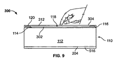
図9は、本明細書で説明および/または図示するタッチスクリーン基板アセンブリの実施態様を含むことができる容量性タッチスクリーンシステム300の断面図である。システム300をいずれの適当なディスプレイ(図示せず)に取り付けてもよく、それは例えばLCDおよび/または偏光を発するいずれかの他の種類のディスプレイであるが、これらに限定されない。例示的な実施形態において、システム300は基板アセンブリ110を含み、先に説明したように、基板アセンブリは、基板112および導電性材料116を含む。システム300は、アセンブリ110のタッチ領域118にわたって配置した絶縁層312も含む。特に、基板112と向き合う絶縁層312の表面302は、基板112上の導電性材料116に直接配置されている。一般的には絶縁層312および/または特に面304の耐久性を向上させるために、絶縁層312は、表面302に対向する表面304上のコーティング(図示せず、限定するわけではないが、例えば無機シリカなど)を含んでよい。場合によっては、基板112の表面204を、少なくとも部分的に透明な導電性材料516によって、少なくとも部分的に被覆してもよい。導電性材料516は、容量結合からおよびディスプレイからの電気的干渉からシステム300を保護するガード電極としての機能を果たすことができる。幾つかの実施態様において、導電性材料516を既知の常套の導電性コーティングから作る。別の態様において、導電性材料516は、導電性材料516がディスプレイに対して所定の透明性を有するように配置したMLCEs(図示せず)を含む。例示的な実施態様において、導電性コーティング516は、ディスプレイが発する偏光の電場の方向に対してほぼ垂直にMLCEsのパターン全体が配向するように配置したMLCEsを含み、導電性材料516が、ディスプレイが発する偏光にほぼ完全に透明であるようにする。
FIG. 9 is a cross-sectional view of a capacitive
表面114に対向する、基板112の表面204は、タッチスクリーンを一緒に用いるディスプレイの面(図示せず)にわたって一般的に配置されている。動作時、タッチ領域118と電気的に接続するプロセッサ(図示せず)は、タッチ領域118に交流電圧またはパルス電圧を適用する。タッチ領域118の内側の箇所にて、絶縁層312のタッチ表面304(または別の態様において、含まれる場合、表面304上のコーティング)を触ることによって、使用者が入力する場合、AC電流が導電性材料116から引き出され、使用者の体を通って地面に流れる。使用者を通って地面に到る電流は、電極120に接続された電気回路(図示せず)によって供給される。電気回路は、使用者の入力を処理するために、そのプロセッサまたはコンピュータもしくは他のデバイスのプロセッサと連絡し、接触部のXおよびY座標の測定を提供する。
The
例示的な実施態様において、システム300は、導電性材料116および導電性材料516の双方を含む。別の態様において、システム300は、材料116または材料516のいずれかを含むだけである。システム200が材料116および材料516の一方を含むだけのそのような実施態様において、含まれていない材料は、既知の常套の導電性コーティングである類似の導電性材料(図示せず)によって置き換えられている。場合によっては、システム300は、基板表面204を少なくとも部分的に被覆するいずれの導電性材料も含まない。
In the exemplary embodiment,
導電性材料516および対応するMLCEsは、導電性材料16(図1〜図3)およびMLCEs22とそれぞれ実質的に同様である。従って、導電性材料16およびMLCEs22の説明および図示を、導電性材料516および対応するMLCEsに適用できる。例えば、導電性材料516の構成、材料構築、構造物の太さ、電気特性、機械特性、利点、適用方法および/または手段ならびに同様のもの、ならびに対応するMLCEsの利点、構成、配置、構造、材料構築配向、寸法、形状および同様のものは、導電性材料16およびMLCEs22のそれとそれぞれ実質的に同様である。従って、導電性材料516および対応するMLCEsを本明細書で更に詳細には説明しない。材料116と同様に、および材料16と異なり、材料516は曲げを被らず、従って、よりもろい構築物であってよい。
絶縁層312を、絶縁層312が本明細書で説明するように機能できるいずれの適当な材料から作ってもよく、それは例えば二酸化ケイ素、ガラス、別の種類の無機層ならびに/または限定するわけではないが、ポリエステル、ポリエチレンテレフタレート(PET)および/もしくはポリエチレンナフタレート(PEN)のようなポリマーフィルムであるが、これらに限定されない。例えば、システム300の特定の用途に基づいて、絶縁層312は、完全に透明または部分的に透明であってよい。幾つかの態様において、絶縁層312の1つまたはそれより多くの部分は不透明であってよい。絶縁層312は、例えば、システム300の特定の用途に応じて、絶縁層312が本明細書で説明するように機能できるいずれの適当な寸法および/または形状を有してもよく、それは例えば矩形、円形、三角形および/または楕円形の形状であるが、これらに限定されない。
The insulating
本明細書で説明および/または図示した実施態様は、導電性材料の所定の度合いの導電率を維持しながら、所定の偏光方向に偏光した光への更なる透明性を有することができる、MLCEに基づく導電性材料を有するタッチスクリーンを提供する。 The embodiments described and / or illustrated herein may have additional transparency to light polarized in a predetermined polarization direction while maintaining a predetermined degree of conductivity of the conductive material. A touch screen having a conductive material based thereon is provided.
例示的な実施態様は、本明細書で詳細に説明および/または図示されている。実施態様は、本明細書で説明する特定の実施態様に限定されず、むしろ、各実施態様の構成部材および/または段階を、本明細書で説明する他の構成部材および/または段階から独立して、かつ別個に利用することができる。1つの実施態様の各構成部材および/または各段階を、他の実施態様の他の構成部材および/または段階と組み合わせて用いることもできる。本明細書で説明および/または図示する要素/構成部材/その他を導入する場合、「1つの」、「その」、「該」および「少なくとも1つの」なる冠詞は、1つまたはそれより多くの要素/構成部材/その他が存在することを意味するように意図されている。「有して成る(含んで成る)」、「含む」および「有する」なる用語は、列挙した要素/構成部材/その他以外の更なる要素/構成部材/その他が存在してもよいことを包括および意味するように意図されている。更に、請求項中の「第1」、「第2」および「第3」などの用語は単なる標識として用いられており、それらの物体に番号順的な要件を課すことは意図されていない。更に、以下の請求項の限定は、更なる構造物の機能が後続する「のための手段」なる記載について明確に言及していない限り、手段+機能のフォーマットで記載されておらず、かつ35U.S.C.§112の第6段落に基づいて解釈されることを意図していない。 Exemplary embodiments are described and / or illustrated in detail herein. The embodiments are not limited to the specific embodiments described herein, but rather the components and / or steps of each embodiment are independent of the other components and / or steps described herein. And can be used separately. Each component and / or each stage of one embodiment can also be used in combination with other components and / or stages of other embodiments. Where the elements / components / others described and / or illustrated herein are introduced, the article “one”, “its”, “the” and “at least one” may include one or more It is intended to mean that an element / component / other exists. The terms “comprising”, “including” and “having” encompass that there may be additional elements / components / others other than the listed elements / components / others. And is meant to mean. Further, terms such as “first”, “second” and “third” in the claims are used merely as labels and are not intended to impose any numerical ordering requirements on those objects. Further, the limitations of the following claims are not described in a means + function format unless explicitly stated in the description of "means for" followed by further structural functions and 35U . S. C. It is not intended to be interpreted under the sixth paragraph of §112.
本発明を種々の特定の実施態様の観点から説明してきたが、当業者は、本発明が請求項の概念および範囲内で、変更を加えて実施できることを理解するだろう。 While the invention has been described in terms of various specific embodiments, those skilled in the art will recognize that the invention can be practiced with modification within the spirit and scope of the claims.
Claims (10)
タッチスクリーンシステムの基板の導電性領域上に配置するように構成した表面を有する絶縁層;および
絶縁層表面の少なくとも一部に配置される導電性材料であって、導電性材料が、第1方向に対して垂直な第2方向に偏光した第2偏光に対してよりも、第1偏光に対して一層透明であるように、第1偏光の第1方向に対して配向するパターンで配置される複数の微小直線状導電性要素を含んで成る導電性材料
を有して成るカバーシートアセンブリ。 A cover sheet assembly for a touch screen system, comprising:
An insulating layer having a surface configured to be disposed on a conductive region of a substrate of the touch screen system; and a conductive material disposed on at least a portion of the surface of the insulating layer, wherein the conductive material is in a first direction Arranged in a pattern oriented with respect to the first direction of the first polarization so that it is more transparent to the first polarization than to the second polarization polarized in the second direction perpendicular to A cover sheet assembly comprising a conductive material comprising a plurality of micro linear conductive elements.
基板;および
基板に導電性タッチ領域を提供するために、基板の表面の少なくとも一部に配置される導電性材料であって、第1方向に対して垂直な第2方向に偏光した第2偏光に対してよりも、第1偏光に対して一層透明であるように、導電性材料が、第1偏光の第1方向に対して配向するパターンで配置された複数の微小直線状導電性要素を含んで成る導電性材料
を有して成る基板アセンブリ。 A substrate assembly for a touch screen system,
And a second polarization polarized in a second direction perpendicular to the first direction, the conductive material disposed on at least a portion of the surface of the substrate to provide a conductive touch area on the substrate A plurality of micro linear conductive elements in which the conductive material is arranged in a pattern oriented with respect to the first direction of the first polarization so that it is more transparent to the first polarization than to A substrate assembly comprising a conductive material comprising.
Applications Claiming Priority (2)
| Application Number | Priority Date | Filing Date | Title |
|---|---|---|---|
| US11/893,041 US8212792B2 (en) | 2007-08-14 | 2007-08-14 | Touchscreen using oriented microscopic linear conductive elements |
| PCT/US2008/009718 WO2009023243A2 (en) | 2007-08-14 | 2008-08-13 | Touchscreen using oriented microscopic linear conductive elements |
Publications (2)
| Publication Number | Publication Date |
|---|---|
| JP2010537275A true JP2010537275A (en) | 2010-12-02 |
| JP2010537275A5 JP2010537275A5 (en) | 2011-09-29 |
Family
ID=40351366
Family Applications (1)
| Application Number | Title | Priority Date | Filing Date |
|---|---|---|---|
| JP2010521037A Pending JP2010537275A (en) | 2007-08-14 | 2008-08-13 | Touch screen using oriented micro linear conductive elements |
Country Status (6)
| Country | Link |
|---|---|
| US (1) | US8212792B2 (en) |
| EP (1) | EP2183662A2 (en) |
| JP (1) | JP2010537275A (en) |
| CN (1) | CN101779186B (en) |
| TW (1) | TW200909935A (en) |
| WO (1) | WO2009023243A2 (en) |
Cited By (5)
| Publication number | Priority date | Publication date | Assignee | Title |
|---|---|---|---|---|
| JP2010253813A (en) * | 2009-04-24 | 2010-11-11 | Nissha Printing Co Ltd | Mat electrically conductive nano-fiber sheet and method of manufacturing the same |
| JP2012221006A (en) * | 2011-04-04 | 2012-11-12 | Fujitsu Component Ltd | Resistance film type touch panel |
| JP2013073449A (en) * | 2011-09-28 | 2013-04-22 | Fujifilm Corp | Stereoscopic image display device having touch panel function, and touch panel |
| JP2013097996A (en) * | 2011-10-31 | 2013-05-20 | Shin Etsu Polymer Co Ltd | Transparent wiring board and input device including the same |
| KR20150029395A (en) * | 2013-09-10 | 2015-03-18 | 동우 화인켐 주식회사 | Hybrid touch sensing electrode and preparing method thereof |
Families Citing this family (20)
| Publication number | Priority date | Publication date | Assignee | Title |
|---|---|---|---|---|
| US8199118B2 (en) * | 2007-08-14 | 2012-06-12 | Tyco Electronics Corporation | Touchscreen using both carbon nanoparticles and metal nanoparticles |
| CN101620454A (en) * | 2008-07-04 | 2010-01-06 | 清华大学 | Potable computer |
| CN101676832B (en) * | 2008-09-19 | 2012-03-28 | 清华大学 | Desktop computer |
| TWI374379B (en) | 2007-12-24 | 2012-10-11 | Wintek Corp | Transparent capacitive touch panel and manufacturing method thereof |
| TWM348999U (en) | 2008-02-18 | 2009-01-11 | Tpk Touch Solutions Inc | Capacitive touch panel |
| KR101482702B1 (en) * | 2008-07-16 | 2015-01-15 | 삼성전자주식회사 | Non-contact touch panel using nanowire |
| JP5493739B2 (en) * | 2009-03-19 | 2014-05-14 | ソニー株式会社 | Sensor device and information processing device |
| CN101995990B (en) * | 2009-08-26 | 2013-01-09 | 群康科技(深圳)有限公司 | Touch panel and positioning method of touch points of same |
| JP5347913B2 (en) * | 2009-11-06 | 2013-11-20 | ソニー株式会社 | SENSOR DEVICE, ELECTRONIC DEVICE, AND METHOD FOR MANUFACTURING SENSOR DEVICE |
| CN102103438A (en) * | 2009-12-18 | 2011-06-22 | 鸿富锦精密工业(深圳)有限公司 | Touch panel |
| JP2011221676A (en) * | 2010-04-07 | 2011-11-04 | Sony Corp | Information presentation device, touch sensation presentation method and program |
| EP2756373B1 (en) | 2011-09-16 | 2017-11-22 | Hewlett-Packard Development Company, L.P. | Positional input systems and methods |
| US9040114B2 (en) | 2012-08-29 | 2015-05-26 | Rohm And Haas Electronic Material Llc | Method of manufacturing silver miniwire films |
| WO2014073597A1 (en) * | 2012-11-08 | 2014-05-15 | アルプス電気株式会社 | Conductor and method for producing same |
| USD742841S1 (en) * | 2013-03-26 | 2015-11-10 | Sony Corporation | Touch sensitive device |
| US9430113B2 (en) * | 2014-05-20 | 2016-08-30 | Eastman Kodak Company | Electrically-conductive article with improved bus region |
| US9405423B2 (en) * | 2014-05-20 | 2016-08-02 | Eastman Kodak Company | Article with electrically-conductive silver connector wire pattern |
| CN104765092A (en) | 2015-04-13 | 2015-07-08 | 京东方科技集团股份有限公司 | Polarizer and manufacturing method thereof and display device |
| TWI618954B (en) * | 2015-05-26 | 2018-03-21 | 住華科技股份有限公司 | Optical film and display module using the same |
| US10884557B2 (en) * | 2017-08-22 | 2021-01-05 | Korea Advanced Institute Of Science And Technology | Touch input device |
Citations (3)
| Publication number | Priority date | Publication date | Assignee | Title |
|---|---|---|---|---|
| JPH02308106A (en) * | 1989-05-23 | 1990-12-21 | Citizen Watch Co Ltd | Linear polarizing light source |
| JP2001188103A (en) * | 1999-01-14 | 2001-07-10 | Sumitomo Chem Co Ltd | Antireflection film |
| US20060274049A1 (en) * | 2005-06-02 | 2006-12-07 | Eastman Kodak Company | Multi-layer conductor with carbon nanotubes |
Family Cites Families (23)
| Publication number | Priority date | Publication date | Assignee | Title |
|---|---|---|---|---|
| US4353552A (en) | 1979-02-23 | 1982-10-12 | Peptek, Incorporated | Touch panel system and method |
| JP3894571B2 (en) | 1995-06-06 | 2007-03-22 | レイケム・コーポレイション | Flexible electrode carrying article |
| US6650319B1 (en) | 1996-10-29 | 2003-11-18 | Elo Touchsystems, Inc. | Touch screen based topological mapping with resistance framing design |
| US6469267B1 (en) | 2000-07-12 | 2002-10-22 | Elo Touchsystems, Inc. | Switch with at least one flexible conductive member |
| US6593916B1 (en) | 2000-11-03 | 2003-07-15 | James L. Aroyan | Touchscreen having multiple parallel connections to each electrode in a series resistor chain on the periphery of the touch area |
| US7106307B2 (en) | 2001-05-24 | 2006-09-12 | Eastman Kodak Company | Touch screen for use with an OLED display |
| US6488981B1 (en) | 2001-06-20 | 2002-12-03 | 3M Innovative Properties Company | Method of manufacturing a touch screen panel |
| US7477242B2 (en) | 2002-05-20 | 2009-01-13 | 3M Innovative Properties Company | Capacitive touch screen with conductive polymer |
| US7180508B2 (en) | 2002-09-17 | 2007-02-20 | Tyco Electronics Corporation | Dynamic corrections for a non-linear touchscreen |
| WO2004052559A2 (en) | 2002-12-06 | 2004-06-24 | Eikos, Inc. | Optically transparent nanostructured electrical conductors |
| WO2004106404A1 (en) | 2003-05-27 | 2004-12-09 | Fujitsu Limited | Organic conductive polymer composition, transparent conductive film and transparent conductor both comprising the composition, and input device comprising the transparent conductor and its manufacturing method |
| US20070128905A1 (en) | 2003-06-12 | 2007-06-07 | Stuart Speakman | Transparent conducting structures and methods of production thereof |
| US7265686B2 (en) | 2003-07-15 | 2007-09-04 | Tyco Electronics Corporation | Touch sensor with non-uniform resistive band |
| GB0316926D0 (en) | 2003-07-18 | 2003-08-27 | Eastman Kodak Co | Method of coating |
| US20050209392A1 (en) | 2003-12-17 | 2005-09-22 | Jiazhong Luo | Polymer binders for flexible and transparent conductive coatings containing carbon nanotubes |
| WO2005086982A2 (en) | 2004-03-12 | 2005-09-22 | Eikos, Inc. | Carbon nanotube stripping solutions and methods |
| US7956287B2 (en) * | 2004-04-20 | 2011-06-07 | Takiron Co., Ltd. | Transparent conductive formed article for a touch panel and touch panel |
| US20060276056A1 (en) | 2005-04-05 | 2006-12-07 | Nantero, Inc. | Nanotube articles with adjustable electrical conductivity and methods of making the same |
| US7593004B2 (en) | 2005-06-02 | 2009-09-22 | Eastman Kodak Company | Touchscreen with conductive layer comprising carbon nanotubes |
| TWI428937B (en) | 2005-08-12 | 2014-03-01 | Cambrios Technologies Corp | Nanowires-based transparent conductors |
| WO2008057615A2 (en) | 2006-03-03 | 2008-05-15 | Eikos, Inc. | Highly transparent and conductive carbon nanotube coatings |
| US7718950B2 (en) | 2006-06-07 | 2010-05-18 | Saraf Ravi F | High resolution thin film tactile device to detect distribution of stimuli on by touch |
| US8199118B2 (en) | 2007-08-14 | 2012-06-12 | Tyco Electronics Corporation | Touchscreen using both carbon nanoparticles and metal nanoparticles |
-
2007
- 2007-08-14 US US11/893,041 patent/US8212792B2/en active Active
-
2008
- 2008-08-11 TW TW97130502A patent/TW200909935A/en unknown
- 2008-08-13 JP JP2010521037A patent/JP2010537275A/en active Pending
- 2008-08-13 EP EP20080827391 patent/EP2183662A2/en not_active Withdrawn
- 2008-08-13 WO PCT/US2008/009718 patent/WO2009023243A2/en active Application Filing
- 2008-08-13 CN CN2008801029724A patent/CN101779186B/en not_active Expired - Fee Related
Patent Citations (3)
| Publication number | Priority date | Publication date | Assignee | Title |
|---|---|---|---|---|
| JPH02308106A (en) * | 1989-05-23 | 1990-12-21 | Citizen Watch Co Ltd | Linear polarizing light source |
| JP2001188103A (en) * | 1999-01-14 | 2001-07-10 | Sumitomo Chem Co Ltd | Antireflection film |
| US20060274049A1 (en) * | 2005-06-02 | 2006-12-07 | Eastman Kodak Company | Multi-layer conductor with carbon nanotubes |
Cited By (6)
| Publication number | Priority date | Publication date | Assignee | Title |
|---|---|---|---|---|
| JP2010253813A (en) * | 2009-04-24 | 2010-11-11 | Nissha Printing Co Ltd | Mat electrically conductive nano-fiber sheet and method of manufacturing the same |
| JP2012221006A (en) * | 2011-04-04 | 2012-11-12 | Fujitsu Component Ltd | Resistance film type touch panel |
| JP2013073449A (en) * | 2011-09-28 | 2013-04-22 | Fujifilm Corp | Stereoscopic image display device having touch panel function, and touch panel |
| JP2013097996A (en) * | 2011-10-31 | 2013-05-20 | Shin Etsu Polymer Co Ltd | Transparent wiring board and input device including the same |
| KR20150029395A (en) * | 2013-09-10 | 2015-03-18 | 동우 화인켐 주식회사 | Hybrid touch sensing electrode and preparing method thereof |
| KR102074168B1 (en) * | 2013-09-10 | 2020-02-06 | 동우 화인켐 주식회사 | Hybrid touch sensing electrode and preparing method thereof |
Also Published As
| Publication number | Publication date |
|---|---|
| EP2183662A2 (en) | 2010-05-12 |
| WO2009023243A2 (en) | 2009-02-19 |
| TW200909935A (en) | 2009-03-01 |
| US20090046078A1 (en) | 2009-02-19 |
| CN101779186A (en) | 2010-07-14 |
| WO2009023243A3 (en) | 2009-08-06 |
| CN101779186B (en) | 2012-11-21 |
| US8212792B2 (en) | 2012-07-03 |
Similar Documents
| Publication | Publication Date | Title |
|---|---|---|
| JP2010537275A (en) | Touch screen using oriented micro linear conductive elements | |
| CN101779187B (en) | Touchscreen using both carbon nanoparticles and metal nanoparticles | |
| US20080192014A1 (en) | Touch screen using carbon nanotube electrodes | |
| Liu et al. | Capillary-force-induced cold welding in silver-nanowire-based flexible transparent electrodes | |
| JP4648451B2 (en) | Electronic element | |
| KR101415583B1 (en) | Touch panel and forming method for the same | |
| CN102063214B (en) | Touch screen and display device | |
| US8105126B2 (en) | Method for fabricating touch panel | |
| US20110032196A1 (en) | Touch panel and display device using the same | |
| US8346316B2 (en) | Personal digital assistant | |
| JP2009146418A (en) | Touch panel and display device using the same | |
| KR101726908B1 (en) | Transparent Electrode Formed having Improved Transmittance and Transparency | |
| JP5374457B2 (en) | Planar body and touch panel | |
| US10932364B2 (en) | Transparent conductive film | |
| CN102478992A (en) | Touch screen | |
| Mackey | 43.1: Invited Paper: Trends and Materials in Touch Sensing | |
| JP2013134208A (en) | Pressure sensitive element containing carbon nanotube | |
| TW201349425A (en) | Touch panel | |
| TW201250800A (en) | Touch panel | |
| JP2009196846A (en) | Manufacturing method of thin film made of one-dimensional nano-material, and manufacturing method of electronic device | |
| CN212515719U (en) | Touch panel with dummy pattern | |
| JP2011175890A (en) | Conductive film | |
| KR20150059332A (en) | Electrod members, touch window with the same and display with the same |
Legal Events
| Date | Code | Title | Description |
|---|---|---|---|
| A521 | Request for written amendment filed |
Free format text: JAPANESE INTERMEDIATE CODE: A523 Effective date: 20110810 |
|
| A621 | Written request for application examination |
Free format text: JAPANESE INTERMEDIATE CODE: A621 Effective date: 20110810 |
|
| A131 | Notification of reasons for refusal |
Free format text: JAPANESE INTERMEDIATE CODE: A131 Effective date: 20120918 |
|
| A711 | Notification of change in applicant |
Free format text: JAPANESE INTERMEDIATE CODE: A711 Effective date: 20121023 |
|
| A601 | Written request for extension of time |
Free format text: JAPANESE INTERMEDIATE CODE: A601 Effective date: 20121217 |
|
| A602 | Written permission of extension of time |
Free format text: JAPANESE INTERMEDIATE CODE: A602 Effective date: 20121225 |
|
| A02 | Decision of refusal |
Free format text: JAPANESE INTERMEDIATE CODE: A02 Effective date: 20130402 |