JP2010537187A - Multi-site probe - Google Patents
Multi-site probe Download PDFInfo
- Publication number
- JP2010537187A JP2010537187A JP2010521495A JP2010521495A JP2010537187A JP 2010537187 A JP2010537187 A JP 2010537187A JP 2010521495 A JP2010521495 A JP 2010521495A JP 2010521495 A JP2010521495 A JP 2010521495A JP 2010537187 A JP2010537187 A JP 2010537187A
- Authority
- JP
- Japan
- Prior art keywords
- semiconductor
- matrix array
- probe
- conductor pin
- pitch
- Prior art date
- Legal status (The legal status is an assumption and is not a legal conclusion. Google has not performed a legal analysis and makes no representation as to the accuracy of the status listed.)
- Pending
Links
Images


Classifications
-
- G—PHYSICS
- G01—MEASURING; TESTING
- G01R—MEASURING ELECTRIC VARIABLES; MEASURING MAGNETIC VARIABLES
- G01R1/00—Details of instruments or arrangements of the types included in groups G01R5/00 - G01R13/00 and G01R31/00
- G01R1/02—General constructional details
- G01R1/06—Measuring leads; Measuring probes
- G01R1/067—Measuring probes
- G01R1/073—Multiple probes
- G01R1/07307—Multiple probes with individual probe elements, e.g. needles, cantilever beams or bump contacts, fixed in relation to each other, e.g. bed of nails fixture or probe card
- G01R1/07314—Multiple probes with individual probe elements, e.g. needles, cantilever beams or bump contacts, fixed in relation to each other, e.g. bed of nails fixture or probe card the body of the probe being perpendicular to test object, e.g. bed of nails or probe with bump contacts on a rigid support
-
- G—PHYSICS
- G01—MEASURING; TESTING
- G01R—MEASURING ELECTRIC VARIABLES; MEASURING MAGNETIC VARIABLES
- G01R31/00—Arrangements for testing electric properties; Arrangements for locating electric faults; Arrangements for electrical testing characterised by what is being tested not provided for elsewhere
- G01R31/28—Testing of electronic circuits, e.g. by signal tracer
- G01R31/2832—Specific tests of electronic circuits not provided for elsewhere
- G01R31/2836—Fault-finding or characterising
- G01R31/2846—Fault-finding or characterising using hard- or software simulation or using knowledge-based systems, e.g. expert systems, artificial intelligence or interactive algorithms
-
- G—PHYSICS
- G01—MEASURING; TESTING
- G01R—MEASURING ELECTRIC VARIABLES; MEASURING MAGNETIC VARIABLES
- G01R31/00—Arrangements for testing electric properties; Arrangements for locating electric faults; Arrangements for electrical testing characterised by what is being tested not provided for elsewhere
- G01R31/28—Testing of electronic circuits, e.g. by signal tracer
- G01R31/2851—Testing of integrated circuits [IC]
- G01R31/2886—Features relating to contacting the IC under test, e.g. probe heads; chucks
- G01R31/2887—Features relating to contacting the IC under test, e.g. probe heads; chucks involving moving the probe head or the IC under test; docking stations
-
- Y—GENERAL TAGGING OF NEW TECHNOLOGICAL DEVELOPMENTS; GENERAL TAGGING OF CROSS-SECTIONAL TECHNOLOGIES SPANNING OVER SEVERAL SECTIONS OF THE IPC; TECHNICAL SUBJECTS COVERED BY FORMER USPC CROSS-REFERENCE ART COLLECTIONS [XRACs] AND DIGESTS
- Y10—TECHNICAL SUBJECTS COVERED BY FORMER USPC
- Y10T—TECHNICAL SUBJECTS COVERED BY FORMER US CLASSIFICATION
- Y10T29/00—Metal working
- Y10T29/49—Method of mechanical manufacture
- Y10T29/49002—Electrical device making
- Y10T29/49117—Conductor or circuit manufacturing
Abstract
半導体ダイのプローブを行うための様々なプローブ基板およびその使用方法を開示する。ある局面では、第1の導体ピンマトリックスアレイおよび第2の導体ピンマトリックスアレイをプローブ基板上に形成することを含む製造方法を提供する。第2の導体ピンマトリックスアレイは、第1の軸に沿って第1のピッチ分、第1の導体ピンマトリックスアレイから離れている。この第1のピッチは、半導体ワークピースの第1の半導体ダイと第2の半導体ダイとの間の第2のピッチと実質的に一致するように選択されている。 Various probe substrates and methods of use thereof are disclosed for probing a semiconductor die. In one aspect, a manufacturing method is provided that includes forming a first conductor pin matrix array and a second conductor pin matrix array on a probe substrate. The second conductor pin matrix array is separated from the first conductor pin matrix array by a first pitch along the first axis. This first pitch is selected to substantially coincide with the second pitch between the first semiconductor die and the second semiconductor die of the semiconductor workpiece.
Description
本発明は、広義には半導体加工に関し、具体的には半導体チップのプローブテストを行うためのシステムおよび方法に関する。 The present invention relates generally to semiconductor processing, and more specifically to a system and method for performing a probe test on a semiconductor chip.
現在の集積回路は、通常、驚くべき複雑さの配置で構成された数千万、あるいは何億ものトランジスタおよび他の回路素子を備えている。当然ながら、膨大な数の回路素子およびそれらの素子を製造するために必要な無数の製造工程が設計仕様を満たすか、または超えることを保証するためには、集積回路のテストが不可欠である。集積回路に通常行われる電気テストの一種は、ウエハーレベルで行われ、プローブシステムとして知られる専用機器を用いて集積回路の特定領域とオーミックコンタクトをとる。オーミックコンタクトをとった後は、プローブシステムのテスターが様々な方法で集積回路を電気的に刺激し、それによって集積回路の様々な機能がテストされる。個々のチップがウエハーからダイシングされ、パッケージに実装された後に、パッケージ用チップのための別の種類のテストが実施される。 Current integrated circuits typically include tens of millions or hundreds of millions of transistors and other circuit elements arranged in a surprisingly complex arrangement. Of course, integrated circuit testing is essential to ensure that the vast number of circuit elements and the myriad manufacturing processes required to manufacture those elements meet or exceed the design specifications. One type of electrical test commonly performed on integrated circuits is performed at the wafer level and makes ohmic contact with specific areas of the integrated circuit using specialized equipment known as a probe system. After making ohmic contact, the tester of the probe system electrically stimulates the integrated circuit in various ways, thereby testing various functions of the integrated circuit. After individual chips are diced from the wafer and mounted in a package, another type of test for packaging chips is performed.
従来のプローブシステムはプローバを備える。プローバは、半導体ウエハーを保持し、その個々のダイが選択的にテスターと接触できるように様々な位置に半導体ウエハーをステップ移動させるように設計された機器である。テスターは、通常、個々のダイの実際的な電気的刺激を行う機器である。ある従来の構成では、プローブカードがプローバに実装され、プローブカードを用いて半導体ウエハーとオーミックコンタクトをとる。プローブカードは、プリント回路基板と、半導体チップパッケージ基板と、プローブヘッドとのスタックから成る。プリント回路基板は、プローブ基板を保持し、半導体ウエハーの集積回路に対して比較的低速のテストを行うように構成されている。プローブ基板は、半導体チップパッケージ基板に設計上類似している。プローブ基板は、一般的に、基板から突出する導体ピンの集合体を備え、それによって、ウエハーの半導体ダイ上の領域とオーミックコンタクトをとる。 A conventional probe system includes a prober. A prober is an instrument designed to hold a semiconductor wafer and step the semiconductor wafer to various positions so that its individual dies can selectively contact the tester. A tester is typically a device that provides practical electrical stimulation of individual dies. In one conventional configuration, a probe card is mounted on a prober, and ohmic contact is made with a semiconductor wafer using the probe card. The probe card includes a stack of a printed circuit board, a semiconductor chip package board, and a probe head. The printed circuit board is configured to hold a probe board and perform a relatively slow test on the integrated circuit of the semiconductor wafer. The probe substrate is similar in design to the semiconductor chip package substrate. The probe substrate generally comprises a collection of conductor pins protruding from the substrate, thereby making ohmic contact with a region on the semiconductor die of the wafer.
従来のプローブ基板の変形例の1つには、集積回路の周辺領域だけではなく、フリップチップタイプの集積回路におけるはんだバンプ等の内部領域とも接触可能なピンアレイを備えたものがある。別の従来のプローブ基板の変形例には、一般的に集積回路の周辺領域とは接触するが、集積回路の内部領域とは接触しないように構成された導体ピンの2つ以上の集合体を備えたものがある。従来の単一アレイプローブ基板は、一度に1つの半導体ダイのプロービングしか行うことができない。従来のデュアルサイトプローブ基板は、マルチサイトプロービングが可能であるが、集積回路の周辺領域のみに限られる。 One modification of a conventional probe substrate includes a pin array that can contact not only the peripheral region of an integrated circuit but also an internal region such as a solder bump in a flip chip type integrated circuit. Another conventional probe substrate variation includes two or more collections of conductor pins that are generally configured to contact the peripheral area of the integrated circuit but not to the internal area of the integrated circuit. There is something to prepare. Conventional single array probe substrates can only probe one semiconductor die at a time. A conventional dual site probe substrate can perform multi-site probing, but is limited only to the peripheral region of the integrated circuit.
従来のプローブシステムのさらなる欠点は、従来のプローブスタックプリント回路基板の性能が低速であることである。従って、ウエハーテストレベルでは、比較的低速なテストのみが行われ得る。あるダイをスクラップであると見なすに足る別の種類の不良や欠陥を特定できる高速テストは、最終的なパッケージテストまで待たなければならない。従って、半導体ウエハー上の1つまたは複数のダイが、ウエハーレベルのテスト中は潜在化しており、パッケージング後の最終テスト中にのみ明らかとなる欠陥を有している場合がしばしばある。その場合には、実際には欠陥のあるダイまでもが、そのような欠陥が発見される前に、ダイシングされ、パッケージングされ、パッケージレベルのテストを受けてしまう。歩留まりを制限する欠陥を製造サイクルのより早い段階で発見することができれば、製造コストおよびテストコストを低減することができる。 A further disadvantage of conventional probe systems is that the performance of conventional probe stack printed circuit boards is slow. Thus, at the wafer test level, only relatively slow tests can be performed. A fast test that can identify another type of defect or defect that is sufficient to consider a die as scrap must wait until the final package test. Thus, one or more dies on a semiconductor wafer are often latent during wafer level testing and often have defects that are only apparent during final testing after packaging. In that case, even the defective dies are actually diced, packaged, and subjected to package level testing before such defects are discovered. If defects that limit yield can be found earlier in the manufacturing cycle, manufacturing and test costs can be reduced.
本発明は、上記欠点の1つ以上による影響を克服または低減することに向けられる。 The present invention is directed to overcoming or reducing the effects of one or more of the above disadvantages.
本発明のある局面によれば、第1の導体ピンマトリックスアレイおよび第2の導体ピンマトリックスアレイをプローブ基板上に形成することを含む製造方法が提供される。第2の導体ピンマトリックスアレイは、第1の軸に沿って第1のピッチ分、第1の導体ピンマトリックスアレイから離れている。第1のピッチは、半導体ワークピースの第1の半導体ダイと第2の半導体ダイとの間の第2のピッチと実質的に一致するように選択されている。 According to an aspect of the present invention, there is provided a manufacturing method including forming a first conductor pin matrix array and a second conductor pin matrix array on a probe substrate. The second conductor pin matrix array is separated from the first conductor pin matrix array by a first pitch along the first axis. The first pitch is selected to substantially match the second pitch between the first semiconductor die and the second semiconductor die of the semiconductor workpiece.
本発明の別の局面によれば、複数の半導体ダイを有する半導体ワークピースの第1の対の半導体ダイに、第1の導体ピンマトリックスアレイおよび第2の導体ピンマトリックスアレイを有するプローブ基板を係合させることを含む方法が提供される。第2の導体ピンマトリックスアレイは、第1の軸に沿って第1のピッチ分、第1の導体ピンマトリックスアレイから離れている。第1のピッチは、半導体ワークピースの第1の対の半導体ダイ間の第2のピッチと実質的に一致するように選択されている。第1の対の半導体ダイに対して電気的プローブテストが行われる。 According to another aspect of the invention, a first pair of semiconductor dies of a semiconductor workpiece having a plurality of semiconductor dies is associated with a probe substrate having a first conductor pin matrix array and a second conductor pin matrix array. A method comprising combining is provided. The second conductor pin matrix array is separated from the first conductor pin matrix array by a first pitch along the first axis. The first pitch is selected to substantially match the second pitch between the first pair of semiconductor dies of the semiconductor workpiece. An electrical probe test is performed on the first pair of semiconductor dies.
本発明の別の局面によれば、第1の導体ピンマトリックスアレイおよび第2の導体ピンマトリックスアレイを有するプローブ基板を含む装置が提供される。第2の導体ピンマトリックスアレイは、第1の軸に沿って第1のピッチ分、第1の導体ピンマトリックスアレイから離れている。第1のピッチは、半導体ワークピースの半導体ダイと第2の半導体ダイとの間の第2のピッチと実質的に一致するように選択されている。 According to another aspect of the invention, an apparatus is provided that includes a probe substrate having a first conductor pin matrix array and a second conductor pin matrix array. The second conductor pin matrix array is separated from the first conductor pin matrix array by a first pitch along the first axis. The first pitch is selected to substantially coincide with the second pitch between the semiconductor die and the second semiconductor die of the semiconductor workpiece.
本発明の上記および他の利点は、以下の詳細な説明を読むことにより、および図面を参照することにより明らかとなるであろう。 These and other advantages of the invention will become apparent upon reading the following detailed description and upon reference to the drawings.
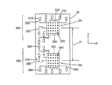
以下に説明する図面において、1以上の図面で同一の構成要素が出てくる場合には、概して同じ参照符号を使用するものとする。次に図面、特に図1には、半導体ワークピースまたはウエハー20の垂直型電気プロービングに適した集積回路プローブカードスタック10(スタック10)の例示的実施形態の分解図が示されている。ウエハー20は、複数の集積回路または半導体ダイを備えており、そのうちの2つを25および27で表している。半導体ワークピース20は、シリコン、ゲルマニウム、または他の半導体材料で構成され得る。所望であれば、ウエハー20は半導体・オン・インシュレータウエハーとして構成されていてもよい。ダイ25および27等のウエハー20のダイは、プロセッサ、特定用途向け集積回路、またはメモリ素子等として機能する集積回路でもよい。ダイ25および27は、座標系29のY軸と平行な軸に沿って測定されるあるピッチP0を隔てて離れている。スタック10は、プローブ基板30、プリント回路基板40、マウンティングブラケット50、およびヘッド60を備える。
In the drawings described below, the same reference numerals are generally used when the same components appear in one or more drawings. Referring now to the drawings, and in particular to FIG. 1, an exploded view of an exemplary embodiment of an integrated circuit probe card stack 10 (stack 10) suitable for vertical electrical probing of a semiconductor workpiece or
プローブ基板30は、Y軸と平行な軸に沿って測定されるあるピッチP1分の間隔を空けた1対のマトリックス型ピンアレイ80および90を備えている。ピッチP1の重要性は後に説明する。以下により詳細に説明するように、プローブ基板30およびそれに付随するピンアレイ80および90を用いることにより、二つの半導体ダイ、例えばダイ25および27のプローブテストを一度に実施することができる。ピンアレイ80および90はマトリックス型であるので、基板30は、周辺チップ領域のみではないデュアルサイト垂直型プロービングを行うことができる。プローブ基板30は、プリント回路基板100から分解された状態で図示されている。スタック10を完全に組み立てた際には、プローブ基板30はプリント回路基板100上に載置される。より具体的には、プローブ基板30を、プリント回路基板100上のボンドパッド領域110上に載置してもよい。ボンドパッド領域110は、複数のはんだバンプ130または他の種類の相互接続構造体から構成され得る相互接続アレイ120を備えている。プローブ基板30は、図1においては不可視であるが、ボンド領域110上の相互接続アレイ120と接合する複数の対応する相互接続構造体を有する。相互接続アレイ120と電気的に接続するために、プローブ基板30は、必要に応じてピングリッドアレイ、ボールグリッドアレイ、ランドグリッドアレイ、または他の種類の相互接続スキームで構成されていてもよい。
The
プリント回路基板100は、1つ以上のいわゆるポゴパッド140および150を備えていてもよい。ポゴパッド140および150は、破線ボックス160で図式化したテスター等の機器と電気的に接続するように設計された複数の上方に突出するバンプまたは他の導体構造体を備える。ポゴパッド140および150は、プリント回路基板100のプローブ基板30の位置とは反対の面170の上に位置するので、透視図で描かれている。パッド140および150の数および位置は、様々な構成要素の中でもプローブ基板30、半導体ウエハー20、およびテスター160のニーズに応じて変化し得る。プリント回路基板100は、複数の導体構造体または配線180を備え、これによりポゴパッド150がボンドパッド110、さらにはプローブ基板30に電気的に接続される。同様に、ポゴパッド160は、複数の導体構造体190によってプローブ基板30と電気的に接続され得る。配線180および190は、基板30の上、内部、またはその双方に位置していてもよい。配線180および190の数およびレイアウトは、設計の裁量にゆだねられる。
The printed
テスター160は、ポゴパッド140および150との接触に用いられるインターフェース200を有していてもよい。テスター160はプリント回路基板100よりかなり大きくてもよいので、図1は一定の縮尺で描かれていないことが理解されるであろう。様々な機器をテスター160に用いることができる。そのシステム例には、例えばTeradyne社のUltraflexおよびAgilentのPinscaleが含まれる。
所望であれば、配線180および190を含むプリント回路基板100は、個々の半導体ダイ25および27の本来のクロック速度より低い速度でウエハーレベルのテストを行うように設計することができる。この点に関して、デュアルサイトフルマトリックスプロービングを行うことができる。しかしながら、ロードボードおよびプローブカードの両方の特性を有するようにプリント回路基板100を調整することによって、付加的な利点を得ることができる。このようにして、プリント回路基板100およびプローブ基板30を用いて個々の半導体ダイ25および27の本来のクロック速度で、またはそれに非常に近い速度でウエハー20のプローブテストを実施することができる。本明細書中の背景の項目に記載したように、従来の垂直型プローブテストは、低いクロック速度のテスト用に装備されたプリント回路基板を用いて行われる。従って、本来約2.0GHzでクロッキングするダイで構成されるウエハーに対して、従来技術では、その速度の数分の一、例えば200〜300MHZでプローブを行い得る。その結果、高速テストは、ダイ25および27のダイシングおよび最終的なパッケージングを待たなければならない。パッケージテストまで待たなければならないことにより、製造業者は、しばしば、最終的に欠陥であると判明するダイに対して、それを知らぬままに加工資源を消費しなければならない。高速の信号伝搬を行うための様々な導体配線180および190を構成するとともに、ボードやカード等を介在させることなく、プローブ基板30をプリント回路基板100に直接実装することにより、ロードボード/プローブカード特性をプリント回路基板100に組み込むことが可能である。
If desired, the printed
マウンティングブラケット50は、ねじ、接着剤、はんだ、または他の周知の締結技術によってプリント回路基板100に接続され得る。ブラケット50は、周知のプラスチック、またはセラミック等から構成され得る。ブラケット50は、ヘッド60を収容する大きさの空間210を含む。さらに、ブラケット50は、ブラケット50がプリント回路基板100上に載置される際にピンアレイ80および90がそこを通って突出することが可能なように設計された開口220を含む。
Mounting
ヘッド60は、プローブ基板30を保護するように設計されたディスク状構造体として構成されていてもよい。ヘッド60は、ねじ、接着剤、はんだ、または他の周知の締結技術によってプリント回路基板100に接続され得る。ヘッド60は、周知のプラスチック、セラミック等から構成され得る。1対の開口240および250がヘッド60に設けられている。開口240および250は、プローブ基板30のピンアレイ80,90の間のピッチP1と一致するピッチP2分の間隔をあけた大きさに作られている。従って、組み立てた際には、ヘッド60は空間210内に位置し、ピンアレイ80および90は、それぞれ開口240および250を通って突出する。
The
プローブテストを行うためには、ウエハー20およびスタック10は共に、破線ボックス260で図式化したプローバ上に載置される。プローバ260は、ウエハー20が上に載置される可動チャック270を備える。チャック270は、通常、X−Y軸によって表される平面等の平面内で移動可能である。チャック270は、Y軸等の所定の軸に沿って、ピッチP3きざみで移動またはステップ移動し得る。1回のステップ移動動作後のチャック270の位置を、破線楕円280によって表す。チャック270のステップ移動ピッチP3は、ダイピッチP0と同じか、それよりも大きくてもよい。プローブ基板30のピンアレイ80および90のピッチP1は、チャック270のステップ移動ピッチP3と一致するように都合良く選択される。もちろん、プローバ260は、典型的には固定位置でプローブスタック10を受けるように動作可能である。スタック10がプローバ260に固定された状態において、テスター160がZ軸と平行に下方に移動し、それによってポゴパッド140および150と接触し、ウエハー20がピンアレイ80および90と接触するまでチャック270がZ軸と平行に上方に移動する。テスト中は、チャック270は様々なダイにステップ移動する。プローバ260として様々な機器を用いることができる。ある例示的実施形態においては、Tokyo Electron model P−12XLを使用してもよい。プローバ260はウエハー20よりかなり大きくてもよいので、図1は一定の縮尺で描かれていないことが理解されるであろう。
In order to perform a probe test, both the
スタック10の様々な構成要素はディスク状構造体として描かれている。しかしながら、当業者には、円以外の形状をプリント回路基板100、ヘッド60、およびマウンティングブラケット50に使用しうることが分かるであろう。
The various components of the
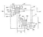
プローブ基板30のさらなる詳細は、俯瞰図である図2を参照することにより理解できるであろう。基板30は、有機物またはセラミック等でもよい。有機物の場合には、基板30は、標準コア、薄型コア、またはコアレスとして製造されていてもよく、周知のエポキシ樹脂およびフィラー等で構成されてもよい。セラミックの場合には、基板30は周知のセラミック材料を用いて構成されていてもよい。図1の説明に関連させて上記したように、ピンアレイ80および90は、図1に示すチャック270のステップ移動ピッチP3と一致するように設計されたピッチP1分の間隔をあけて設けられてもよい。
Further details of the
図2を続けて参照すると、ピンアレイ80は、ボンド領域300上に配置された黒点290によって表されるピンのマトリックスアレイから成る。本明細書中で用いられるように、マトリックスアレイという用語は、集積回路の中央部位および周辺部位との係合に適したピンの配置を意味するものとする。マトリックスアレイは、行および列の数が等しくても、等しくなくてもよく、アレイの各位置にピンを含んでいてもいなくてもよい。ピン290は、様々な導体材料、例えば金、銅、銀、アルミニウム、白金、タンタル、ニッケル、またはこれらの混合物から成っていてもよい。ボンド領域300は、フリップチップが実装された集積回路に用いられる種類のボンド領域と実質的に同一に構成されてもよい。例えば、ボンド領域は、ピン290がそれぞれ接着される複数のはんだ構造体を含んでいてもよい。実際、プローブ基板30の性能目標は、図1に示すウエハー20の半導体ダイ25および27の1つと共に使用するのに適した半導体チップパッケージ基板の電気的挙動を可能な限り模倣することである。ほとんどの半導体チップパッケージ基板は、フィルタリングや他の要件のための複数のコンデンサおよび他の素子を含む。従って、プローブ基板30およびそのピンアレイ80は、複数の受動素子310および相互接続スキーム320を含む回路網システム305を備えていてもよい。相互接続スキーム320は、複数の相互接続体または導体配線で構成されていてもよく、その幾つかを符号330により表している。導体配線330は、図2に示すように表面に位置する配線から構成されてもよいし、基板30の内部に位置するために図2には示されていない導体構造体および相互接続体から構成されてもよい。この場合もやはり、相互接続スキーム320および受動素子310は、半導体チップ用のパッケージ基板の電気的挙動を可能な限り模倣することを意図していることに留意されたい。受動素子310は、コンデンサ、インダクタ、レジスタ、または他の種類の素子から構成されていてもよい。配線330は、様々な導体材料、例えば金、銅、銀、アルミニウム、白金、タンタル、ニッケル、またはこれらの混合物から構成されていてもよい。
With continued reference to FIG. 2, the
ピンアレイ90も同様に、ボンディング領域350上にマトリックス状の形態で配列される黒点340によって表される複数のピンから構成される。ピンアレイ80と同様に、ピンアレイ90は、相互接続スキーム370によってピン340および基板30の他の領域と接続される複数の受動素子360を含む回路網システム355を備えている。相互接続スキーム370は、その幾つかが符号380で表した複数の導体配線から構成される。相互接続スキーム370は、スキーム200の導体配線210と実質的に同じでもよい。
Similarly, the
図2に示すプローブ基板30のレイアウトを作るための例示的方法は、2つの半導体チップパッケージ基板のレイアウト390および400の俯瞰図である図3を参照することにより理解できる。レイアウト390は、基板410、複数のボンド部位430を含むボンディング領域420、複数の受動素子440、および1以上の導体配線460から構成される相互接続スキーム450の設計を含む。レイアウト390は、従来の垂直型プローブテスト用のシングルサイトプローブ基板として同様に用いられる半導体チップパッケージ基板の典型的なレイアウトと似ている。
An exemplary method for creating the layout of the
レイアウト400も同様に、基板470および複数のバンプ部位490を含むボンディング領域480の設計から構成される。複数の受動素子500および複数の配線520から構成される相互接続スキーム510もまた設けられている。2つのレイアウト390および400は、基本的に鏡像複写であると考えられる。図2に示すプローブ基板30のレイアウトを作るためには、相互接続スキーム450および510の分断を最小限に抑えるという目的で、矢印530および540で示すように、基板30等の1つの基板上に作成される単一のレイアウトへと2つのレイアウト390および400を統合する。本明細書の他の箇所に記載したように、ピンアレイ80を含む回路網およびピンアレイ90を含む回路網の電気的挙動が2つのパッケージ基板の実際の電気的挙動を可能な限り模倣するようにプローブ基板30を設計することが望ましい。
The
上記の例示的実施形態では、プローブ基板30のピンアレイ80および90は、プローブ基板30の一端とほぼ平行な任意に選択されたY軸に沿って位置合わせされる。しかしながら、例えば、ピンアレイの他の位置合わせとして、ウエハー上で互い違いの位置関係にある半導体ダイに対する同時プロービングを実施できるような位置合わせをすることも可能である。この点に関して、図4は、ピンアレイ80´および90´をそれぞれ備えたプローブ基板30´の別の例示的実施形態の俯瞰図を示す。ピンアレイ80´および90´は、X軸に沿った水平ピッチP4およびY軸に沿った縦ピッチP5を有して互い違いに配列される。縦および水平という用語は、任意のものとする。プローブ基板30´は、開示された他の実施形態に関して本明細書中の他の箇所に概して記載したのと同じ材料および同じ構造から構成されていてもよい。ピンアレイ80´および90´は、ボンディング領域550および560上にそれぞれ形成されていてもよい。また複数のピン570および580でそれぞれ構成されていてもよい。ピンアレイ80´は、相互接続スキーム600によって、複数の受動素子590および他の電気的構造体を含む回路網システム585に接続され得る。相互接続スキーム600は複数の配線を含み、そのうちの2つを符号610で表している。ピンアレイ90´も同様に、複数の受動素子620と、1つ以上の配線640から成る相互接続スキーム630とを有する回路網システム615を備えていてもよい。
In the exemplary embodiment described above, the
開示された他の実施形態と同様に、プローブ基板30´は、所望であれば同時にではあるが、図4に開示したような互い違いのレイアウトにある2つの半導体チップパッケージ基板の電気的挙動を模倣するように設計されている。ピッチP4およびP5は、図1に示すウエハー20等の所与のウエハー上に互い違いに配置されている2つの半導体ダイの間のピッチと一致するように、または図1に示すプローブ機器チャック270のステップ移動動作のピッチと一致するように設計されてもよい。さらに、ピッチP4およびP5は、等しくても、等しくなくてもよい。
As with the other disclosed embodiments, the probe substrate 30 'mimics the electrical behavior of two semiconductor chip package substrates in a staggered layout as disclosed in FIG. 4, but at the same time if desired. Designed to be. The pitches P 4 and P 5 match the pitch between two semiconductor dies that are staggered on a given wafer, such as
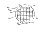
図5は、複数の半導体ダイを含む例示的半導体ウエハー650の俯瞰図である。そのうちの幾つかのダイを、個々に660、670、680、690、700、710、および715の符号で表している。ダイ660、670、680、および690は、縦列720に位置する。ダイ700および710も同様に縦列730に位置し、ダイ715は、縦列740に位置する。図1および2に示される種類のプローブ基板の設計を用いて、様々なパターンで半導体ダイを同時にプローブすることができる。例えば、ピッチP1およびP3(図1を参照)に基づき、縦列720のダイ660および670を同時にプローブした後、縦列720に関してダイ680および690等の同時プローブを実施してもよい。ピッチP1およびP3が隣接するダイよりも大きい場合には、ダイ660とダイ680とが同時にプローブされ、その次に、縦列720のダイ670および690等の組み合わせに対する同時プローブが実施されてもよい。他の縦列730および740等に関しても同じことが言える。もちろん、直交する方向に沿って構成されたダイ、例えばダイ660および710やこれら2つのダイに平行な他のダイが同時にプローブされたり、あるいは少なくともプローブ位置が一定の一般位置にある状態でプローブされ得るように、プローブ基板30(図1および図2を参照)の方向を合わせてもよい。
FIG. 5 is an overhead view of an
図4に示す基板30´の場合のようにプローブ基板を互い違いの設計で構成した場合には、例えば、ダイ660およびダイ700を同時にプローブし、その次に、ダイ710およびダイ715等を同時にプローブし、残りのダイに関しても同様にプローブしてもよい。この場合もやはり、ウエハー650上のダイがプローブされる正確な順番は、図2および図4に開示されるピッチP1、P4、およびP5等のピッチ、並びに、プローブカード30または30´が接続される機器の利用可能なステップ移動ピッチによって決まる。
When the probe substrate is configured in a staggered design as in the case of the
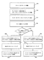
図6は、本明細書中に開示されたようなマルチサイトプローブ基板および改良型ロードボード構成プローブスタックを利用した例示的なテストおよび製造方法のフローチャートである。ステップ750では、ウエハーをプローバに搭載する。例えば、図1に示した半導体ウエハー20を例示されたプローバ260に搭載してもよい。次に、ステップ760では、本明細書中に開示される種類のプローブカードスタック、例えばスタック10をプローバに設置する。ステップ770では、図1に示すテスター160等のテスターをプローブカードスタックと係合させる。この時点で、または所望であればこれ以前に、ステップ780に示したようにプローブテストの速度レベルを選択する。例えば、プローブテストの速度レベルをハイレベルに選択してもよい。このレベルは、ウエハー上の集積回路の本来のクロック速度レベル、または比較的それに近いレベルである。例えば、図1に示すウエハー20のダイは、例えば2.0GHzの設計上の本来のクロック速度を有していてもよい。2.0GHzという数字は単なる例示である。ウエハー20によっては、ウエハー上のダイの本来のクロック速度に幅があり、幾つかのチップは他のチップよりもクロック数が速い。選択肢として、プローブテストの速度レベルを低レベルに選択してもよい。このレベルは、ウエハー上のチップの本来のクロック速度よりも低い速度レベルである。選択されたテスト速度レベルは、テスターの制御システムに入力される。複数のダイがそれぞれの本来のクロック速度でテストされ得ることに留意されたい。次に、ステップ790に示したように、高レベルテストまたは低レベルテストのどちらを行うかの決定がテスターによって行われる。高速レベルテストが選択された場合には、次にステップ800において、ウエハーに対して高速マルチサイトテストが行われ、それによってそのウエハーに関して良品ダイの集合が特定される。高速マルチサイトテストは、ウエハーのダイに対して行われる様々な種類の電気的テストから構成され得る。そのテストの例を幾つか挙げると、スキャン、スキャンチェーン、プログラマブル論理、入出力XOR、デジタル/アナログ変換、内部ループバック、ユニバーサルシリアルバス、PCIエクスプレス、およびシリアルATAが含まれる。テストの数および種類は、ウエハー上のダイの種類およびテスターやプローバの能力による。良品ダイの集合が特定されれば、ウエハーをダイシングして、良品ダイを欠陥品ダイから分けることができる。次に、ステップ810に示すように、良品ダイをパッケージングすることができる。ここでの利点は、高速テストによって良品ダイであると特定されたダイのみがパッケージングおよび最終テストに供される点である。欠陥品ダイのパッケージングおよび最終テストに伴う材料費および人件費を削減することができる。次に、ステップ820に示されるように、パッケージングされた良品ダイは、1つ以上のパッケージテスト、例えば、オペレーティングシステムテスト、パワーショートテスト、スキャン、および入出力XORテスト等を受けることができる。上記のように、このパッケージテストは、先に特定された良品ダイの集合に対してのみ行えばよい。
FIG. 6 is a flowchart of an exemplary test and manufacturing method utilizing a multi-site probe substrate and an improved load board configuration probe stack as disclosed herein. In
一方、ステップ790において低速テストに移るようにテスターがプログラミングされている場合には、ステップ830において、ウエハーのダイに対して低速マルチサイトテストが行われ、それによって良品ダイの集合を特定することができる。ここで、例示的なテストを幾つか挙げると、スキャン、スキャンチェーン、プログラマブル論理、入出力XOR等が含まれ得る。ステップ830で特定された良品ダイの集合は、実際には欠陥品であるが低速テストのみでは特定できないダイを含んでいる場合がある。次に、ステップ840で示すように、ステップ830における低速テストによって特定された良品ダイの集合に対するダイシングおよびパッケージングを行う。最後に、ステップ850において、パッケージングされた良品ダイは最終的なパッケージテストを受けることができる。ステップ830、840、および850が実施されたとしても、半導体ウエハー上の個々のダイに対してより効率的なプローブテストを行うことが可能なマルチサイトマトリックスアレイプローブ基板を使用することによって、意味のある効率化を実現し得る。
On the other hand, if the tester is programmed to move to the low speed test in
本明細書に開示したプローブ基板30および30´は、2つのピンアレイ80および90、または80´および90´を備えている。しかしながら、当業者であれば、本明細書に開示したプローブ基板30および30´の実施形態のいずれもが、2つ以上のピンアレイを備えていてもよく、それによって2つ以上のダイがプローブされ得ることを理解するであろう。
The probe substrates 30 and 30 'disclosed herein include two
本発明は、様々な改変および代替の形態が可能であるが、具体的な実施形態を例として図面に示し、かつ本明細書において詳細に説明した。しかしながら、本発明は、開示された特定の形態に限定されるものではないことに留意されたい。むしろ、本発明は、以下に添付する請求項によって規定されるような本発明の精神および範囲に含まれるあらゆる改変例、均等物、および代替例を包含するものである。 While the invention is susceptible to various modifications and alternative forms, specific embodiments have been shown by way of example in the drawings and have been described in detail herein. However, it should be noted that the invention is not limited to the particular forms disclosed. On the contrary, the invention is intended to cover all modifications, equivalents, and alternatives falling within the spirit and scope of the invention as defined by the claims appended below.
Claims (23)
前記プローブ基板上に第2の導体ピンマトリックスアレイを形成することとを、含み、
前記第2の導体ピンマトリックスアレイは、第1の軸に沿って第1のピッチ分、前記第1の導体マトリックスアレイから離れており、当該第1のピッチは、半導体ワークピースの第1の半導体ダイと第2の半導体ダイとの間の第2のピッチと実質的に一致するように選択されている、製造方法。 Forming a first conductor pin matrix array on a probe substrate;
Forming a second conductor pin matrix array on the probe substrate; and
The second conductor pin matrix array is separated from the first conductor matrix array by a first pitch along a first axis, the first pitch being the first semiconductor of the semiconductor workpiece. A manufacturing method selected to substantially coincide with a second pitch between the die and the second semiconductor die.
請求項1に記載の方法。 A first network system electrically connected to the first conductor pin matrix array on the probe substrate and a second electrically connected to the second conductor pin matrix array on the probe substrate. The first network system has a first layout that provides electrical characteristics of a package substrate adapted to the first semiconductor die, and the second network system includes: The network system has a second layout that provides electrical characteristics of a package substrate adapted to the second semiconductor die;
The method of claim 1.
請求項2に記載の方法。 Forming the first network system includes forming a plurality of first passive elements and a plurality of first interconnects, and forming the second network system includes a plurality of Forming a second passive element and a plurality of second interconnects,
The method of claim 2.
請求項1に記載の方法。 The first and second conductor pin matrix arrays are formed such that the second conductor pin matrix array is separated from the first conductor pin matrix array by a third pitch along a second axis. The third pitch is selected to substantially coincide with a fourth pitch between the first semiconductor die and the second semiconductor die of the semiconductor workpiece;
The method of claim 1.
前記第1の対の半導体ダイに対して電気的プローブテストを行うこととを、含む方法。 A probe substrate having a first conductor pin matrix array and a second conductor matrix array thereon for a first pair of semiconductor dies of a semiconductor workpiece having a plurality of semiconductor dies, the probe substrate comprising: A conductor pin matrix array is spaced from the first conductor pin matrix array by a first pitch along a first axis, the first pitch being the first pair of semiconductor dies of the semiconductor workpiece. Engaging a probe substrate of a configuration selected to substantially match a second pitch between
Conducting an electrical probe test on the first pair of semiconductor dies.
前記第1の対の半導体ダイを実質的にそれぞれの本来のクロック速度でプローブテストするように適合させた回路網を有するプリント回路基板に前記プローブ基板を連結することを含む、請求項8に記載の方法。 One of the first pair of semiconductor dies has a first native clock speed and the other of the first pair of semiconductor dies has a second native clock speed;
9. The probe board of claim 8, comprising coupling the probe board to a printed circuit board having circuitry adapted to probe test the first pair of semiconductor dies substantially at respective native clock rates. the method of.
前記第3の導体ピンマトリックスアレイを用いて前記複数の半導体ダイの内の別の半導体ダイに対して電気的プローブテストを行うことが含まれる、請求項8に記載の方法。 The probe substrate includes a third conductor pin matrix array;
The method of claim 8, comprising performing an electrical probe test on another semiconductor die of the plurality of semiconductor dies using the third conductor pin matrix array.
前記第2の導体ピンマトリックスアレイは、第1の軸に沿って第1のピッチ分、前記第1の導体マトリックスアレイから離れており、当該第1のピッチは、半導体ワークピースの第1の半導体ダイと第2の半導体ダイとの間の第2のピッチと実質的に一致するように選択されている、装置。 A probe substrate having a first conductor pin matrix array and a second conductor pin matrix array;
The second conductor pin matrix array is separated from the first conductor matrix array by a first pitch along a first axis, the first pitch being the first semiconductor of the semiconductor workpiece. An apparatus selected to substantially coincide with a second pitch between the die and the second semiconductor die.
Applications Claiming Priority (2)
| Application Number | Priority Date | Filing Date | Title |
|---|---|---|---|
| US11/840,587 US7847568B2 (en) | 2007-08-17 | 2007-08-17 | Multi-site probe |
| PCT/IB2008/002158 WO2009024851A2 (en) | 2007-08-17 | 2008-08-15 | Multi-site probe |
Publications (2)
| Publication Number | Publication Date |
|---|---|
| JP2010537187A true JP2010537187A (en) | 2010-12-02 |
| JP2010537187A5 JP2010537187A5 (en) | 2011-09-15 |
Family
ID=40328863
Family Applications (1)
| Application Number | Title | Priority Date | Filing Date |
|---|---|---|---|
| JP2010521495A Pending JP2010537187A (en) | 2007-08-17 | 2008-08-15 | Multi-site probe |
Country Status (6)
| Country | Link |
|---|---|
| US (1) | US7847568B2 (en) |
| EP (1) | EP2183603B1 (en) |
| JP (1) | JP2010537187A (en) |
| KR (1) | KR101365188B1 (en) |
| CN (1) | CN101821634B (en) |
| WO (1) | WO2009024851A2 (en) |
Families Citing this family (7)
| Publication number | Priority date | Publication date | Assignee | Title |
|---|---|---|---|---|
| KR20100069300A (en) * | 2008-12-16 | 2010-06-24 | 삼성전자주식회사 | Probe card, and apparatus and method for testing semiconductor device |
| US8519729B2 (en) | 2010-02-10 | 2013-08-27 | Sunpower Corporation | Chucks for supporting solar cell in hot spot testing |
| US9716031B2 (en) | 2014-04-08 | 2017-07-25 | Nxp Usa, Inc. | Semiconductor wafer and method of concurrently testing circuits formed thereon |
| US9997423B2 (en) | 2014-04-08 | 2018-06-12 | Nxp Usa, Inc. | Semiconductor wafer and method of concurrently testing circuits formed thereon |
| CN104615018A (en) * | 2014-12-18 | 2015-05-13 | 西安华芯半导体有限公司 | Method for adjusting DC parameter of simultaneously tested chip |
| US10620236B2 (en) * | 2017-06-12 | 2020-04-14 | Marvell Asia Pte, Ltd. | Multi-test type probe card and corresponding testing system for parallel testing of dies via multiple test sites |
| CN117199055A (en) * | 2022-06-01 | 2023-12-08 | 长鑫存储技术有限公司 | Packaging structure, manufacturing method thereof and semiconductor device |
Citations (5)
| Publication number | Priority date | Publication date | Assignee | Title |
|---|---|---|---|---|
| JPH06177318A (en) * | 1991-09-30 | 1994-06-24 | Internatl Business Mach Corp <Ibm> | Multichip-integrated-circuit package and its system |
| JP2003007784A (en) * | 2001-06-22 | 2003-01-10 | Hitachi Maxell Ltd | Semiconductor inspecting device |
| JP2005302917A (en) * | 2004-04-09 | 2005-10-27 | Renesas Technology Corp | Method of manufacturing semiconductor integrated circuit and probe card |
| WO2006028238A1 (en) * | 2004-09-06 | 2006-03-16 | Nec Corporation | Test carrier |
| JP2007017363A (en) * | 2005-07-11 | 2007-01-25 | Japan Electronic Materials Corp | Probe card |
Family Cites Families (19)
| Publication number | Priority date | Publication date | Assignee | Title |
|---|---|---|---|---|
| US4038599A (en) * | 1974-12-30 | 1977-07-26 | International Business Machines Corporation | High density wafer contacting and test system |
| US4692205A (en) * | 1986-01-31 | 1987-09-08 | International Business Machines Corporation | Silicon-containing polyimides as oxygen etch stop and dual dielectric coatings |
| JP3219844B2 (en) * | 1992-06-01 | 2001-10-15 | 東京エレクトロン株式会社 | Probe device |
| US5642056A (en) * | 1993-12-22 | 1997-06-24 | Tokyo Electron Limited | Probe apparatus for correcting the probe card posture before testing |
| US6258609B1 (en) * | 1996-09-30 | 2001-07-10 | Micron Technology, Inc. | Method and system for making known good semiconductor dice |
| US6404212B1 (en) * | 1999-02-18 | 2002-06-11 | St Assembly Test Services Pte Ltd | Testing of BGA and other CSP packages using probing techniques |
| JP2000260852A (en) * | 1999-03-11 | 2000-09-22 | Tokyo Electron Ltd | Inspection stage and device |
| US6812718B1 (en) * | 1999-05-27 | 2004-11-02 | Nanonexus, Inc. | Massively parallel interface for electronic circuits |
| JP2001056346A (en) | 1999-08-19 | 2001-02-27 | Fujitsu Ltd | Probe card and method for testing wafer on which a plurality of semiconductor device are formed |
| US6407568B1 (en) * | 2000-02-10 | 2002-06-18 | International Business Machines Corporation | Apparatus for probing ends of pins |
| US6441629B1 (en) * | 2000-05-31 | 2002-08-27 | Advantest Corp | Probe contact system having planarity adjustment mechanism |
| JP2002122630A (en) * | 2000-10-17 | 2002-04-26 | Ando Electric Co Ltd | Ic tester adjustment device |
| JP2002168906A (en) * | 2000-11-28 | 2002-06-14 | Ando Electric Co Ltd | Device for connecting test head |
| US6547409B2 (en) * | 2001-01-12 | 2003-04-15 | Electroglas, Inc. | Method and apparatus for illuminating projecting features on the surface of a semiconductor wafer |
| US6674296B1 (en) * | 2002-02-28 | 2004-01-06 | Advanced Micro Devices, Inc. | Probe card measurement tool |
| US20050212546A1 (en) * | 2004-03-26 | 2005-09-29 | Mark Lynch | Method and apparatus for package testing |
| EP1906215A4 (en) | 2005-07-14 | 2012-04-18 | Teijin Chemicals Ltd | Foamed resin sheet and liquid crystal display |
| US7821283B2 (en) | 2005-12-22 | 2010-10-26 | Jsr Corporation | Circuit board apparatus for wafer inspection, probe card, and wafer inspection apparatus |
| TW200729373A (en) * | 2006-01-20 | 2007-08-01 | Advanced Semiconductor Eng | Test module for wafer |
-
2007
- 2007-08-17 US US11/840,587 patent/US7847568B2/en active Active
-
2008
- 2008-08-15 WO PCT/IB2008/002158 patent/WO2009024851A2/en active Application Filing
- 2008-08-15 CN CN200880111413.XA patent/CN101821634B/en active Active
- 2008-08-15 KR KR1020107005841A patent/KR101365188B1/en active IP Right Grant
- 2008-08-15 EP EP08806888A patent/EP2183603B1/en active Active
- 2008-08-15 JP JP2010521495A patent/JP2010537187A/en active Pending
Patent Citations (5)
| Publication number | Priority date | Publication date | Assignee | Title |
|---|---|---|---|---|
| JPH06177318A (en) * | 1991-09-30 | 1994-06-24 | Internatl Business Mach Corp <Ibm> | Multichip-integrated-circuit package and its system |
| JP2003007784A (en) * | 2001-06-22 | 2003-01-10 | Hitachi Maxell Ltd | Semiconductor inspecting device |
| JP2005302917A (en) * | 2004-04-09 | 2005-10-27 | Renesas Technology Corp | Method of manufacturing semiconductor integrated circuit and probe card |
| WO2006028238A1 (en) * | 2004-09-06 | 2006-03-16 | Nec Corporation | Test carrier |
| JP2007017363A (en) * | 2005-07-11 | 2007-01-25 | Japan Electronic Materials Corp | Probe card |
Also Published As
| Publication number | Publication date |
|---|---|
| EP2183603A2 (en) | 2010-05-12 |
| KR101365188B1 (en) | 2014-02-21 |
| WO2009024851A2 (en) | 2009-02-26 |
| US7847568B2 (en) | 2010-12-07 |
| KR20100055483A (en) | 2010-05-26 |
| CN101821634B (en) | 2013-08-14 |
| WO2009024851A3 (en) | 2009-04-30 |
| US20090045827A1 (en) | 2009-02-19 |
| CN101821634A (en) | 2010-09-01 |
| EP2183603B1 (en) | 2012-10-31 |
Similar Documents
| Publication | Publication Date | Title |
|---|---|---|
| US6551844B1 (en) | Test assembly including a test die for testing a semiconductor product die | |
| US6429029B1 (en) | Concurrent design and subsequent partitioning of product and test die | |
| US6456099B1 (en) | Special contact points for accessing internal circuitry of an integrated circuit | |
| JP2011128159A (en) | Method and device for measuring signal | |
| JP2010537187A (en) | Multi-site probe | |
| CN103887193B (en) | Device for three dimensional integrated circuits test | |
| KR100580405B1 (en) | Test assembly including a test die for testing a semiconductor product die | |
| JP4343256B1 (en) | Manufacturing method of semiconductor device | |
| CN110531125B (en) | Space transformer, probe card and manufacturing method thereof | |
| US7535239B1 (en) | Probe card configured for interchangeable heads | |
| JP3318671B2 (en) | Multi-chip module and test chip manufacturing method | |
| KR101458119B1 (en) | Probe card | |
| US20030234660A1 (en) | Direct landing technology for wafer probe | |
| KR101509198B1 (en) | Separatable contactor for Probe card | |
| KR200468020Y1 (en) | Probe package and probe card having the same |
Legal Events
| Date | Code | Title | Description |
|---|---|---|---|
| A521 | Written amendment |
Free format text: JAPANESE INTERMEDIATE CODE: A523 Effective date: 20110801 |
|
| A621 | Written request for application examination |
Free format text: JAPANESE INTERMEDIATE CODE: A621 Effective date: 20110801 |
|
| A977 | Report on retrieval |
Free format text: JAPANESE INTERMEDIATE CODE: A971007 Effective date: 20130213 |
|
| A131 | Notification of reasons for refusal |
Free format text: JAPANESE INTERMEDIATE CODE: A131 Effective date: 20130219 |
|
| A601 | Written request for extension of time |
Free format text: JAPANESE INTERMEDIATE CODE: A601 Effective date: 20130517 |
|
| A602 | Written permission of extension of time |
Free format text: JAPANESE INTERMEDIATE CODE: A602 Effective date: 20130524 |
|
| A521 | Written amendment |
Free format text: JAPANESE INTERMEDIATE CODE: A523 Effective date: 20130814 |
|
| A131 | Notification of reasons for refusal |
Free format text: JAPANESE INTERMEDIATE CODE: A131 Effective date: 20140603 |
|
| A521 | Written amendment |
Free format text: JAPANESE INTERMEDIATE CODE: A523 Effective date: 20140829 |
|
| A02 | Decision of refusal |
Free format text: JAPANESE INTERMEDIATE CODE: A02 Effective date: 20150317 |