JP2010531493A - Adaptive control method of logic strip based on multi-channel non-volatile solid-state memory - Google Patents
Adaptive control method of logic strip based on multi-channel non-volatile solid-state memory Download PDFInfo
- Publication number
- JP2010531493A JP2010531493A JP2010513626A JP2010513626A JP2010531493A JP 2010531493 A JP2010531493 A JP 2010531493A JP 2010513626 A JP2010513626 A JP 2010513626A JP 2010513626 A JP2010513626 A JP 2010513626A JP 2010531493 A JP2010531493 A JP 2010531493A
- Authority
- JP
- Japan
- Prior art keywords
- logic
- logic strip
- channel
- strip
- storage device
- Prior art date
- Legal status (The legal status is an assumption and is not a legal conclusion. Google has not performed a legal analysis and makes no representation as to the accuracy of the status listed.)
- Pending
Links
- 238000000034 method Methods 0.000 title claims abstract description 35
- 230000003044 adaptive effect Effects 0.000 title claims abstract description 15
- 238000003860 storage Methods 0.000 claims abstract description 74
- 230000008569 process Effects 0.000 claims abstract description 11
- 230000003993 interaction Effects 0.000 claims abstract description 3
- 239000007787 solid Substances 0.000 claims 1
- 238000005192 partition Methods 0.000 description 13
- 230000008901 benefit Effects 0.000 description 4
- 238000004519 manufacturing process Methods 0.000 description 3
- 238000013507 mapping Methods 0.000 description 2
- GHOSNRCGJFBJIB-UHFFFAOYSA-N Candesartan cilexetil Chemical compound C=12N(CC=3C=CC(=CC=3)C=3C(=CC=CC=3)C3=NNN=N3)C(OCC)=NC2=CC=CC=1C(=O)OC(C)OC(=O)OC1CCCCC1 GHOSNRCGJFBJIB-UHFFFAOYSA-N 0.000 description 1
- 238000009826 distribution Methods 0.000 description 1
- 230000006870 function Effects 0.000 description 1
- 230000004044 response Effects 0.000 description 1
- 230000000630 rising effect Effects 0.000 description 1
- 239000004065 semiconductor Substances 0.000 description 1
- 238000000638 solvent extraction Methods 0.000 description 1
Images

Classifications
-
- G—PHYSICS
- G11—INFORMATION STORAGE
- G11C—STATIC STORES
- G11C16/00—Erasable programmable read-only memories
- G11C16/02—Erasable programmable read-only memories electrically programmable
- G11C16/06—Auxiliary circuits, e.g. for writing into memory
- G11C16/10—Programming or data input circuits
-
- G—PHYSICS
- G06—COMPUTING; CALCULATING OR COUNTING
- G06F—ELECTRIC DIGITAL DATA PROCESSING
- G06F12/00—Accessing, addressing or allocating within memory systems or architectures
- G06F12/02—Addressing or allocation; Relocation
- G06F12/0223—User address space allocation, e.g. contiguous or non contiguous base addressing
- G06F12/023—Free address space management
- G06F12/0238—Memory management in non-volatile memory, e.g. resistive RAM or ferroelectric memory
- G06F12/0246—Memory management in non-volatile memory, e.g. resistive RAM or ferroelectric memory in block erasable memory, e.g. flash memory
-
- G—PHYSICS
- G06—COMPUTING; CALCULATING OR COUNTING
- G06F—ELECTRIC DIGITAL DATA PROCESSING
- G06F2212/00—Indexing scheme relating to accessing, addressing or allocation within memory systems or architectures
- G06F2212/72—Details relating to flash memory management
- G06F2212/7202—Allocation control and policies
-
- G—PHYSICS
- G06—COMPUTING; CALCULATING OR COUNTING
- G06F—ELECTRIC DIGITAL DATA PROCESSING
- G06F2212/00—Indexing scheme relating to accessing, addressing or allocation within memory systems or architectures
- G06F2212/72—Details relating to flash memory management
- G06F2212/7208—Multiple device management, e.g. distributing data over multiple flash devices
Landscapes
- Engineering & Computer Science (AREA)
- Theoretical Computer Science (AREA)
- Physics & Mathematics (AREA)
- General Engineering & Computer Science (AREA)
- General Physics & Mathematics (AREA)
- Techniques For Improving Reliability Of Storages (AREA)
- Read Only Memory (AREA)
Abstract
本発明は、マルチチャンネル非揮発性固体記憶装置に基づくロジック・ストリップの適応制御方法を提供する。各チャンネル内の記憶スペースを、同じサイズを有する複数の記憶ユニットに分割するステップ1と、各チャンネルにおける離散的な物理アドレスを持っている記憶ユニットを連続的なロジックスペースに構成するための少なくとも一つのロジック・ストリップを設定するとともに、ロジック・ストリップによって一体に纏められる記憶ユニットを確定するための、ロジック・ストリップのパラメータを設定するステップ2と、記憶装置の操作履歴情報を統計し、統計した操作履歴情報に基づいて動的にロジック・ストリップのパラメータの値を調整するステップ3と、データのインタラクションを行う過程において、ロジック・ストリップのパラメータによってデータを分割して各チャンネル内の記憶ユニットにマッピングするとともに、チャンネル毎にデータの読み書き操作を並行して実行するステップ4とを含む。
【選択図】図2The present invention provides an adaptive control method for logic strips based on multi-channel non-volatile solid-state storage devices. Step 1 for dividing the storage space in each channel into a plurality of storage units having the same size, and at least one for configuring the storage units having discrete physical addresses in each channel into a continuous logic space. Set up two logic strips and set the logic strip parameters to determine the storage units that are bundled together by the logic strip. In step 3 of dynamically adjusting logic strip parameter values based on historical information and in the process of data interaction, the data is divided by the logic strip parameters and mapped to storage units in each channel. Together with And a step 4 which concurrently executes read and write operations of data for each tunnel.
[Selection] Figure 2
Description
本発明は非揮発性固体記憶装置のロジックスペースの構成方法に関し、より詳細には、マルチチャンネル非揮発性固体記憶装置に基づくロジック・ストリップ(Logic Strip)の適応制御方法に関する。 The present invention relates to a method for configuring a logic space of a non-volatile solid-state storage device, and more particularly, to an adaptive control method for a logic strip based on a multi-channel non-volatile solid-state storage device.
記憶装置の分野において、ハードディスクは主導的な地位を占めているが、従来、半導体を記憶媒体とする非揮発性固体記憶装置が次第にディスクのかわりに主導的な地位を占めてきていおり、例えば、フラッシュメモリはその例の一つである。以下、フラッシュメモリを例として非揮発性固体記憶装置の特徴を説明する。フラッシュメモリは、複数回の読み書き、消去が可能なだけではなく、密度が高い、容量が大きい、読み書き操作時間が短い、及び不揮発性、電力消費が低いなどの長所を持つために、ますます記憶装置の市場において新しい勢力になり、その市場シェアが急速に上昇してきている。特に近年、フラッシュメモリの生産技術が成熟し、値段が安くなり、同時に、後端アプリケーション技術も進んでいるため、フラッシュメモリの市場は急速に拡大し、メモリ分野においてハードディスクと同じ市場シェアを占めている。しかし、製造方法の問題により、自体の避けられない欠点が存在している、例えば、フラッシュメモリチップがリード・ライトの操作を実行する時はセクタ単位でなければならないことや、各フラッシュメモリチップのリード・ライトの帯域は40MBを超えることができないことなどである。これらの欠点がフラッシュメモリの発展を制約し、そのアプリケーションの過程において、以上のような障害を解決しないことには、フラッシュメモリの長所を揮発できない。 In the field of storage devices, hard disks occupy a leading position, but in the past, non-volatile solid-state storage devices that use semiconductors as storage media have gradually occupied a leading position instead of disks. Flash memory is one example. Hereinafter, features of the non-volatile solid-state storage device will be described using a flash memory as an example. Flash memory not only can be read and written multiple times, but also has advantages such as high density, large capacity, short read / write operation time, non-volatility, low power consumption, etc. It has become a new force in the equipment market, and its market share is rising rapidly. Especially in recent years, flash memory production technology has matured, its price has become cheaper, and at the same time, rear-end application technology has advanced, so the flash memory market has expanded rapidly and has the same market share as hard disks in the memory field. Yes. However, due to problems in the manufacturing method, there are unavoidable disadvantages of the flash memory chip. For example, when a flash memory chip performs a read / write operation, it must be in units of sectors, For example, the read / write bandwidth cannot exceed 40 MB. These disadvantages limit the development of the flash memory, and the advantages of the flash memory cannot be volatilized without solving the above obstacles in the course of its application.
フラッシュメモリのアプリケーションの技術の発展に伴い、ユーザの記憶装置の読み書きの効率への要望も高まり、シングルチップ或いはシングルチャンネルフラッシュメモリのインターフェースのリード・ライトのレートでは既にユーザの要望に答えることができない。そのため、ほとんど全てのフラッシュメモリ及びフラッシュメモリコントローラの製造者がマルチチャンネルフラッショメモリチップの操作モードを研究している。このマルチチャンネルフラッショメモリはマルチチャンネルで同時にフラッシュメモリの操作を実行することができるので、フラッシュメモリのインターフェースのリード" ライトのテートを何倍にも拡大させるという長所がある。 With the development of flash memory application technology, the demand for read / write efficiency of users' storage devices has increased, and the read / write rate of single-chip or single-channel flash memory interface cannot already meet the user's demands. . For this reason, almost all flash memory and flash memory controller manufacturers are studying the operating modes of multi-channel flash memory chips. This multi-channel flash memory has the advantage that the read / write state of the flash memory interface can be expanded many times because the flash memory can be operated simultaneously in multiple channels.
このようなマルチチャンネルのフラッシュメモリに対して、マルチチャンネルが同時にホストからの命令を実施することと、並列的に読み書き、消去などの操作を行うことが必要であるので、書き込まれたデータ或いは読み取られたデータに対して、どのようにそれを構成するか及びどのようにマルチチャンネルでの離散的な物理記憶スペースを構成するかという問題は避けられず、従来の技術では、これらの問題をうまく解決できる方法がないである。 For such multi-channel flash memory, it is necessary for the multi-channel to simultaneously execute commands from the host and to perform operations such as reading / writing and erasing in parallel. The problem of how to configure the given data and how to configure the multi-channel discrete physical storage space is unavoidable, and the conventional technology successfully solves these problems. There is no solution.
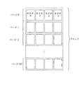
一つの方法とは、並列的な操作を実行する各チャンネルにの記憶ユニットの個数を固定することである。即ち、記憶装置の各ロジック・ストリップでの各チャンネルの記憶ユニットの個数が固定されている。図2に示すように、フラッシュメモリのファームウェアは保留区の情報によって、n個のチャンネルにおける各チャンネルのmページが一つのロジック・ストリップを構成することを指示する(図の例ではnは4、mは2である)。その中でページは一つの記憶ユニットである。全てのロジック・ストリップを連続させて一つの連続的なロジック記憶スペースになり、即ちユーザが見える装置の記憶スペースである。 One method is to fix the number of storage units in each channel that performs parallel operations. That is, the number of storage units of each channel in each logic strip of the storage device is fixed. As shown in FIG. 2, the flash memory firmware indicates that the m pages of each channel in the n channels constitute one logic strip according to the reserved area information (in the example shown, n is 4, m is 2.) Among them, a page is a storage unit. All logic strips are contiguous into one continuous logic storage space, i.e. the storage space of the device visible to the user.
しかし、使用過程において、この構成方法は下記の問題が現れてきている。フラッシュメモリは様々なユーザに対応し、各ユーザにはそれぞれの目的がある。例えば、一部のユーザは主にフラッシュメモリに記憶させる或いは常にデータを書き込む必要がある。このような場合、もしロジック・ストリップが比較的小さいにパーテションすれば、各ライト操作でマルチチャンネルのフラッシュメモリチップを起動することが必要となり、目的ページにデータが既に存在すれば、目的ブロックにおける有効的なデータをバックアップしてから、当該ブロックを消去し、最後に有効的なデータ及び当該操作のデータを書き込む。故に、当該書き込み過程において、ロジック・ストリップが小さければ小さいほど、消去が必要となるブロックが多くなり、より多くの操作時間が必要となると同時にフラッシュメモリにもより多くの損耗をもたらす。もしロジック・ストリップのサイズが比較的大きければ、一回の書き込み操作をできるだけ一つのチャンネルに落とし、目的ブロックは一回の消去操作だけで当該書き込み操作を実現できることになり、書き込み操作にかかる時間が大幅に節約できると同時にフラッシュメモリの損耗も有効的に減少させることができる。さらにもう一つ例とすれば、一部のユーザはフラッシュメモリに比較的小さいサイズのファイルをバックアップするだけで、使用過程ではそれらのファイルの読み取りだけが必要である。このような場合は、もしロジック・ストリップのサイズが比較的大きければ、毎回一つだけのリード操作が起動されるので、リード操作の過程において、データを一つのチャンネルに落とし、操作過程において、一つだけのチャンネルが起動されるので、データの並列的な操作が実現できないことになり、フラッシュメモリのインターフェースのリードのレートを大幅に低くする。もしロジック・ストリップが比較的小さくできれば、データが複数のチャンネルに分布されるので、操作過程において複数のチャンネルが同時に起動され、フラッシュメモリのインターフェースのリードスピードが何倍にも上がることになる。 However, in the process of use, this configuration method has the following problems. The flash memory corresponds to various users, and each user has a purpose. For example, some users need to be mainly stored in flash memory or always write data. In such a case, if the logic strip is partitioned to a relatively small size, it is necessary to start a multi-channel flash memory chip for each write operation. If data already exists on the target page, it is valid for the target block. After the data is backed up, the block is erased, and finally valid data and operation data are written. Thus, in the writing process, the smaller the logic strip, the more blocks that need to be erased, requiring more operation time and at the same time causing more wear on the flash memory. If the size of the logic strip is relatively large, one write operation can be reduced to one channel as much as possible, and the target block can realize the write operation by only one erase operation. At the same time as savings, flash memory wear can be effectively reduced. As yet another example, some users only need to back up files of relatively small size to flash memory and only need to read those files during use. In such a case, if the logic strip size is relatively large, only one read operation is activated each time, so in the read operation process, data is dropped into one channel and Since only one channel is activated, data parallel operation cannot be realized, greatly reducing the read rate of the flash memory interface. If the logic strip can be made relatively small, the data is distributed over a plurality of channels, so that the channels are activated simultaneously during the operation process, and the read speed of the flash memory interface is increased several times.
前記の内容によって、ロジック・ストリップの適切なパーティションはフラッシュメモリに大きい影響を与えることわかる。しかし、従来のフラッシュメモリのロジック・ストリップのパーティションは製造時に固定されているので、たとえ異なる使用目的を持ったユーザに対しても、そのロジック・ストリップは固定されたままであり、使用過程においてリード" ライトの効率及び寿命に大きな影響を与えることになる。故に、どのように有効的にロジック・ストリップをパーティションするかという問題を解決するかどうかがマルチチャンネルフラッシュメモリに非常に大きな影響を与える。 From the above, it can be seen that the appropriate partition of the logic strip has a large impact on the flash memory. However, because the partition of the conventional flash memory logic strip is fixed at the time of manufacture, the logic strip remains fixed even for users with different usage purposes, It will have a significant impact on the efficiency and lifetime of the light, so whether to solve the problem of how to effectively partition the logic strip will have a huge impact on multi-channel flash memory.
従来の非揮発性固定記憶装置では、操作を実施する過程において、ロジック・ストリップが固定されるので、異なる状況に応じて調整できない。その問題に対して、本発明は、マルチチャンネル非揮発性固体記憶装置に基づくロジック・ストリップの適応制御方法を提供し、非揮発性固体記憶装置自体に統計の機能を備えることによって、ロジック・ストリップに対してを制御を行い、知的にロジック・ストリップのサイズを調整する。それによってロジック・ストリップのサイズが適切ではないことため生じた問題を解決できる。 In the conventional nonvolatile fixed storage device, the logic strip is fixed in the process of performing the operation, and therefore cannot be adjusted according to different situations. In response to this problem, the present invention provides a method for adaptive control of a logic strip based on a multi-channel non-volatile solid-state storage device, and by providing the statistical function in the non-volatile solid-state storage device itself, And control the logic strip size intelligently. This solves problems caused by the incorrect size of the logic strip.
本発明は、マルチチャンネル非揮発性固体記憶装置に基づくロジック・ストリップの適応制御方法であって、
各チャンネル内の記憶スペースを、同じサイズを有する複数の記憶ユニットに分割するステップ1と、
各チャンネルにおける離散的な物理アドレスを持っている記憶ユニットを連続的なロジックスペースに構成するための少なくとも一つのロジック・ストリップを設定するとともに、ロジック・ストリップによって一体に纏められる(Organize)記憶ユニットを確定するための、ロジック・ストリップのパラメータを設定するステップ2と、
記憶装置の操作履歴情報を統計し、統計した操作履歴情報に基づいて動的にロジック・ストリップのパラメータの値を調整するステップ3と、
データのインタラクションを行う過程において、ロジック・ストリップのパラメータによってデータを分割して各チャンネル内の記憶ユニットにマッピングするとともに、チャンネル毎にデータの読み書き操作を並行して実行するステップ4とを含む。
The present invention is a method for adaptive control of a logic strip based on a multi-channel non-volatile solid-state storage device, comprising:
Dividing the storage space in each channel into a plurality of storage units having the same size; and
Set up at least one logic strip to organize the storage units with discrete physical addresses in each channel into a continuous logic space and organize the storage units together by the
In the process of performing the data interaction, the process includes the step 4 of dividing the data according to the logic strip parameters and mapping the data to the storage unit in each channel and executing the data read / write operation in parallel for each channel.
前記ステップ3において、操作履歴情報は操作データブロックのサイズ、操作タイプ、操作回数のうちの少なくとも一つを含むことが望ましい。
In
前記統計した操作履歴情報に基づいて動的にロジック・ストリップのパラメータの値を調整するステップにおいて、各操作タイプの出現頻度に基づいてロジック・ストリップのパラメータの値を確定することが望ましい。 In the step of dynamically adjusting the value of the logic strip parameter based on the statistical operation history information, it is preferable to determine the value of the logic strip parameter based on the appearance frequency of each operation type.
前記各操作タイプの出現頻度に基づいてロジック・ストリップのパラメータの値を調整するステップにおいて、各操作タイプがそれぞれ一つのロジック・ストリップのパラメータ値に対応するように、非揮発性固体記憶装置において調整を行う操作回数のしきい値を設定し、非揮発性固体記憶装置において行う各種操作の回数を統計し、統計した回数が前記しきい値に達すると、ロジック・ストリップのパラメータ値を、操作回数の一番多い操作タイプに対応するロジック・ストリップのパラメータ値に調整することが望ましい。 In the step of adjusting the value of the parameter of the logic strip based on the frequency of appearance of each operation type, adjustment is made in the non-volatile solid-state memory so that each operation type corresponds to the parameter value of one logic strip. The number of operations to be performed is set, the number of various operations performed in the non-volatile solid-state storage device is statistics, and when the number of statistics reaches the threshold, the parameter value of the logic strip is set to the number of operations. It is desirable to adjust the parameter value of the logic strip corresponding to the operation type having the largest number of operations.
前記ステップ2において、前記ロジック・ストリップのパラメータは、ロジック・ストリップのサイズに対応し、或いは、各チャンネルにおいて一つのロジック・ストリップを介してロジック的に接続される記憶ユニットの個数に対応することが望ましい。
In the
前記記憶ユニットはそれぞれ一つのロジック・ストリップのパラメータに対応することが望ましい。 Each of the storage units preferably corresponds to one logic strip parameter.
前記記憶ユニットはセクター、ページ或いはバイトであることが望ましい。 The storage unit is preferably a sector, a page, or a byte.
前記ロジック・ストリップのパラメータは、記憶ユニットの冗長区に記憶されるか、記憶装置に纏めて記憶されることが望ましい。 The logic strip parameters are preferably stored in a redundant section of the storage unit or collectively stored in a storage device.
前記非揮発性固体記憶装置はフラッシュメモリを含むことが望ましい。 The nonvolatile solid-state storage device preferably includes a flash memory.
ロジック・ストリップのパラメータ値に対する調整が必要である場合、記憶装置に記憶されている既存データをバックアップすることを更に含むことが望ましい。 If adjustment to the parameter values of the logic strip is necessary, it is desirable to further include backing up existing data stored in the storage device.
記憶装置を複数のロジック・ブロックに分割し、分割した各ロジック・ブロックに対して、それぞれステップ1、ステップ2、ステップ3、ステップ4という順に読み書き制御を行うことが望ましい。
It is desirable to divide the storage device into a plurality of logic blocks and perform read / write control on the divided logic blocks in the order of Step 1,
本発明のマルチチャンネル非揮発性固体記憶装置に基づくロジック・ストリップの適応制御方法は、主な利点として、ロジック・ストリップのパーティションが変化でき、記憶装置において操作履歴の記録に基づいてアルゴリズムを使って適応的にロジック・ストリップのサイズを設定できることが取り上げられる。本発明では、装置がより良くユーザの要望に応えられると共に、非揮発性固体記憶装置の操作効率を高め、フラッシュメモリの使用寿命を延ばすことができる。 The logic strip adaptive control method based on the multi-channel non-volatile solid-state storage device of the present invention has the main advantage that the partition of the logic strip can be changed and uses an algorithm based on the record of operation history in the storage device. It is taken up that the size of the logic strip can be set adaptively. According to the present invention, the device can better meet the needs of the user, increase the operation efficiency of the nonvolatile solid-state storage device, and extend the service life of the flash memory.
本発明の重点は、適応的なアルゴリズムを通して非揮発性固体記憶装置の操作履歴記録によってロジック・ストリップのサイズを設定することにより、様々な使用範囲とユーザに適応させるとともに非揮発性固体記憶装置のリード・ライト操作の効率を上げ、使用寿命を引き伸ばすことである。以下、フラッシュメモリを非揮発性固体記憶装置の典型な実施例として詳細に説明する。他の記憶装置に対する実現原理はフラッシュメモリと本質的に同じである。 The emphasis of the present invention is to adapt the size of the logic strip by recording the operation history of the non-volatile solid-state storage device through an adaptive algorithm, thereby adapting it to various usage ranges and users as well as the non-volatile solid-state storage device. It is to increase the efficiency of read / write operations and extend the service life. Hereinafter, the flash memory will be described in detail as a typical example of a non-volatile solid-state storage device. The implementation principle for other storage devices is essentially the same as for flash memory.
図1を参照し、フラッシュメモリをパーティションすることは例として説明する。各バイトは8ビットを含み、528バイトが一つのセクタを構成し、その中には512バイトの有効なデータ区と16バイトの冗長区が含まれ、4セクタが一つのページになり、64ページが一つの物理ブロックになる。マルチチャンネルのフラッシュメモリについては、図2に示すように、nチャンネルでの各チャンネルのmページが一つのロジック・ストリップを構成する。そのうち、nの値は固定された、装置のチャンネルの個数であり、mの値は装置の策略によって決まる。 Referring to FIG. 1, partitioning the flash memory will be described as an example. Each byte contains 8 bits, 528 bytes make up one sector, which contains 512 bytes of valid data section and 16 bytes of redundant section, 4 sectors become one page, 64 pages Becomes one physical block. In the multi-channel flash memory, as shown in FIG. 2, m pages of each channel in n channels constitute one logic strip. Of these, the value of n is the number of fixed device channels, and the value of m is determined by the strategy of the device.
本実施例はページを記憶ユニットとし、ロジック・ストリップというのはファームウェアがフラッシュメモリチップの物理ページをパーティションする方法である。マルチチャンネルのフラッシュメモリがマルチチャンネルで同時に操作を実行するため、書き込まれたデータ或いは読み取られたデータは必ず異なるラッシュメモリチップにある。故に、物理スペースの分布が連続していない。しかし、ロジックスペースへのマッピングや構成は必ず連続しなければならない。或いは、ロジック・ストリップがこれらの連続していない物理ページを一つの連続するロジックスペースに構成する。 In this embodiment, a page is a storage unit, and a logic strip is a method by which firmware partitions a physical page of a flash memory chip. Since multi-channel flash memory performs operations simultaneously on multiple channels, written data or read data is always in different rush memory chips. Therefore, the physical space distribution is not continuous. However, the mapping and configuration to the logic space must be continuous. Alternatively, the logic strip configures these non-contiguous physical pages into one continuous logic space.
図2のは、マルチチャンネルのフラッシュメモリのロジック・ストリップのパーティションである。図で示した例のチャンネルの個数は4、ロジック・ストリップでの各フラッシュメモリのページの個数は2である。従って、本例で示されたマルチチャンネルのフラッシュメモリのロジック・ストリップのサイズは図に示した開始ロジック・ストリップ0と任意のロジック・ストリップX のように、16KBである。 FIG. 2 shows a logic strip partition of a multi-channel flash memory. The number of channels in the example shown in the figure is 4, and the number of pages in each flash memory in the logic strip is 2. Therefore, the size of the logic strip of the multi-channel flash memory shown in this example is 16 KB, like the starting logic strip 0 and the optional logic strip X shown in the figure.
以下、図面を参照し、具体的な実施例で本発明を詳細に説明する。 Hereinafter, the present invention will be described in detail by way of specific examples with reference to the drawings.
フラッシュメモリの操作タイプのランクを2K、4K、8Kに設定する。2Kより小さいリード、2Kより小さいライト、2K−4Kのリード、2K−4Kのライト、4K−8Kのリード、4K−8Kのライト、8Kより大きいリード、8Kより大きいライトなどの操作タイプがある。チャンネルの個数は4で、そのうち各ランクが対応する最適化のロジック・ストリップの値は本実施例ではそれぞれ、2Kより小さいリード、2Kより小さいライト、2K−4Kのリード、4K−8Kのリード、8Kより大きいリードに対応するロジック・ストリップが8K、2K−4Kのライトに対応するロジック・ストリップが16K、4K−8Kのライト、8Kより大きいライトに対応するロジック・ストリップが32Kというタイプがある。操作回数のしきい値を10000回に設定する、即ち、フラッシュメモリが10000回に操作される毎に、フラッシュメモリのロジック・ストリップを適応的に調整する。 Set the flash memory operation type rank to 2K, 4K, or 8K. There are operation types such as read smaller than 2K, write smaller than 2K, read 2K-4K, write 2K-4K, read 4K-8K, write 4K-8K, read larger than 8K, write larger than 8K. The number of channels is 4, and the value of the optimized logic strip corresponding to each rank is less than 2K, less than 2K, less than 2K, 2K-4K, 4K-8K, There are 8K logic strips corresponding to leads larger than 8K, 16K logic strips corresponding to 2K-4K writes, 4K-8K writes, and 32K logic strips corresponding to writes larger than 8K. The threshold of the number of operations is set to 10000 times, that is, each time the flash memory is operated 10,000 times, the logic strip of the flash memory is adjusted adaptively.
フラッシュメモリのファームウェアはフラッシュメモリの操作履歴情報を統計し、それをフラッシュメモリ保留情報区に保存する。統計する操作履歴情報には操作データブロックのサイズ、操作のタイプ、操作の回数のうち少なくても一つがあり、本実施例においては、各操作タイプに対応する操作の回数を統計することである。操作の回数が10000回に達する毎に、異なるタイプの操作を比較し、装置のロジック・ストリップのサイズを使用頻度の最も高い操作に対応するランクに設定する。 The flash memory firmware statistics the operation history information of the flash memory and stores it in the flash memory holding information section. There is at least one of the operation data block size, the operation type, and the number of operations in the operation history information to be statistics. In this embodiment, the number of operations corresponding to each operation type is statistics. . Each time the number of operations reaches 10,000, different types of operations are compared and the size of the logic strip of the device is set to the rank corresponding to the most frequently used operation.
図3に示すように、ユーザはフラッシュメモリ或いはフラッシュメモリのあるロジックパーティションから頻繁的に容量が小さいデータを読み取るだけの場合、2Kより小さいリード、2Kより小さいライト或いは2K以上のデータのリードのうちいずれかの操作タイプの使用頻度がほかのタイプより大きい場合は、フラッシュメモリがこれらの操作過程におけるスピードを保証するために、本発明の実施例を使うことによって、ロジック・ストリップに適応した調整ができるようになる。図に示すように、データが平均で2Kより小さければ、ロジック・ストリップのサイズは適応的に8Kに調整される。そうすれば、各回の書き込む操作を一つのチャンネルに落とし、ライト操作のスピードを十分に上げることができるようになると同時にできるだけ多くのリード操作を並列的に実行するという原則に一致する。フラッシュメモリ或いはロジックブロックが頻繁に2k以上のデータを読み取る時に、ロジック・ストリップが最小のランク(例えば、8k)を選択する。そうすれば、データを読み取る時に、できるだけ多くのチャンネルが起動され、十分的に記憶装置のインターフェースの読み取るスピードを上げることができる。 As shown in Fig. 3, when the user only reads data with small capacity frequently from flash memory or a logic partition with flash memory, read less than 2K, write less than 2K, or read more than 2K data If the frequency of use of one of the operation types is greater than the other types, the flash memory can be adjusted to accommodate the logic strip by using embodiments of the present invention to ensure speed in these operations. become able to. As shown, if the average data is less than 2K, the size of the logic strip is adaptively adjusted to 8K. If this is done, the write operation of each time can be reduced to one channel, the speed of the write operation can be sufficiently increased, and at the same time, as many read operations as possible are executed in parallel. When the flash memory or logic block frequently reads 2k or more data, the logic strip selects the lowest rank (eg, 8k). Then, when reading data, as many channels as possible are activated, and the reading speed of the storage device interface can be sufficiently increased.
図4に示すように。8kより大きいライト、或いは4k−8kのライトのうちいずれかの操作タイプの使用頻度が他のタイプの使用頻度より大きければ、図に示すように、ロジック・ストリップのサイズを32Kに調整する。ユーザがフラッシュメモリに頻繁に書き込む操作が必要である場合に、フラッシュメモリの書き込み操作過程における効率とインターフェースのスピード及びフラッシュメモリチップにの損耗を減らすのを保証することを考慮した上で、本発明を通してロジック・ストリップに適応した調整し、ロジック・ストリップのサイズを32Kに設定する。各チャンネルのフラッシュメモリチップには新しいデータを書き込む前に、まず目的ブロックでの古いデータを消去する。この消去操作が非常に時間がかかり、かつフラッシュメモリチップの損耗つながるので、毎回できるだけ少ないチャンネルを起動することが必要となる。操作過程においては、ロジック・ストリップのパーティションが大きければ大きいほど、消去操作が少なければ少ないほど、操作にかかる時間とフラッシュメモリチップの損耗が少なくなる。即ち、フラッシュメモリのインターフェースのライトのレートが有効的に上げられると同時に装置の使用寿命を引き伸ばすことができる。 As shown in Figure 4. If the usage frequency of any of the operation types of the light larger than 8k or the light of 4k-8k is larger than the usage frequency of the other types, the size of the logic strip is adjusted to 32K as shown in the figure. In consideration of ensuring efficiency and interface speed in flash memory write operation process and reducing flash memory chip wear when a user frequently needs to write to flash memory. And adjust the size of the logic strip to 32K. Before writing new data to the flash memory chip of each channel, the old data in the target block is first erased. Since this erase operation is very time consuming and leads to wear of the flash memory chip, it is necessary to activate as few channels as possible each time. In the process of operation, the larger the partition of the logic strip, the fewer erase operations, the less time it takes to operate and the wear of the flash memory chip. That is, the flash memory interface write rate can be effectively increased and at the same time the service life of the device can be extended.
その他、フラッシュメモリはロジック・ストリップのパラメータを調整する時、フラッシュメモリで記憶した有効なデータをバックアップする必要がある。ソフトウェアを使って自動的にバックアップしてもいいし、ロジック・ストリップのパラメータを調整する前に、ヒューマン" マシン" インターフェースがユーザーへ記憶装置のデータをバックアップするよう提示をすることも良い。 In addition, when the flash memory adjusts the parameters of the logic strip, it is necessary to back up valid data stored in the flash memory. It can be backed up automatically using software, or the human “machine” interface can be presented to the user to back up storage data before adjusting the parameters of the logic strip.
フラッシュメモリが複数のロジックパーティションを含む状況に対しては、各ロジックパーティションがそれぞれに異なるロジック・ストリップのパラメータがある。装置はユーザの異なるパーティション、異なる使用目的によって、自動的にロジック・ストリップのサイズを調整することができる。 For situations where the flash memory includes multiple logic partitions, each logic partition has a different logic strip parameter. The device can automatically adjust the size of the logic strip according to the user's different partitions and different usage purposes.
前記の実施形態によって本発明を説明したが、本発明を実現する方法には複数のタイプがあり、その主な目的は自動的に適応させるアルゴリズムを使ってフラッシュメモリのヒストリー操作の記録によってロジック・ストリップのサイズを設定することによって、フラッシュメモリのリード" ライト操作のスピードと効率を上がると同時にフラッシュメモリの使用寿命を引き伸ばす。本発明は一種の実施例を例として説明したが、本発明を実現する方法には複数のタイプがあり、類似した変化は本発明の主導的な考えのもとである上に、技術者にとっても顕然なことである。また、本発明で出した非揮発性固体記憶装置がNANDやNORなどのフラッシュメモリチップだけではなく、ほかの類似したロジック・ストリップ構成の記憶装置も本発明の主導思想ち適用範囲から離脱せず、関連する技術者にとっても顕然な変化のため、すべて本発明の範囲に属する。 Although the present invention has been described by the above embodiments, there are multiple types of methods for implementing the present invention, the main purpose of which is to record logic operations by recording history operations of flash memory using an automatically adapting algorithm. Setting the size of the strip increases the speed and efficiency of the flash memory read and write operations and at the same time extends the useful life of the flash memory. While the present invention has been described by way of an example embodiment, the present invention is realized. There are several types of methods, and similar changes are not only based on the lead idea of the present invention but also obvious to engineers. The solid-state storage device is not only a flash memory chip such as NAND or NOR, but also other similar logic strip storage devices. Without leaving from the spirit Chi scope, for Kenzen changes even for related technicians, all within the scope of the present invention.
Claims (11)
各チャンネル内の記憶スペースを、同じサイズを有する複数の記憶ユニットに分割するステップ1と、
各チャンネルにおける離散的な物理アドレスを持っている記憶ユニットを連続的なロジックスペースに構成するための少なくとも一つのロジック・ストリップを設定するとともに、ロジック・ストリップによって一体に纏められる記憶ユニットを確定するための、ロジック・ストリップのパラメータを設定するステップ2と、
記憶装置の操作履歴情報を統計し、統計した操作履歴情報に基づいて動的にロジック・ストリップのパラメータの値を調整するステップ3と、
データのインタラクションを行う過程において、ロジック・ストリップのパラメータによってデータを分割して各チャンネル内の記憶ユニットにマッピングするとともに、チャンネル毎にデータの読み書き操作を並行して実行するステップ4と、
を含むことを特徴とするマルチチャンネル非揮発性固体記憶装置に基づくロジック・ストリップの適応制御方法。 A method for adaptive control of a logic strip based on a multi-channel non-volatile solid-state storage device, comprising:
Dividing the storage space in each channel into a plurality of storage units having the same size; and
To set up at least one logic strip for configuring storage units having discrete physical addresses in each channel into a continuous logic space and to determine the storage units that are grouped together by the logic strip Step 2 of setting the logic strip parameters
Step 3 for statistically processing the storage device operation history information and dynamically adjusting the value of the logic strip parameter based on the statistical operation history information;
In the process of data interaction, the data is divided according to the logic strip parameters and mapped to the storage unit in each channel, and the data read / write operation is performed in parallel for each channel, step 4,
A method for adaptive control of a logic strip based on a multi-channel non-volatile solid-state storage device.
各操作タイプがそれぞれ一つのロジック・ストリップのパラメータ値に対応するように、非揮発性固体記憶装置において調整を行う操作回数のしきい値を設定し、
非揮発性固体記憶装置において行う各種操作の回数を統計し、統計した回数が前記しきい値に達すると、ロジック・ストリップのパラメータ値を、操作回数の一番多い操作タイプに対応するロジック・ストリップのパラメータ値に調整することを特徴とする請求項3に記載のマルチチャンネル非揮発性固体記憶装置に基づくロジック・ストリップの適応制御方法。 Adjusting the value of the parameter of the logic strip based on the frequency of appearance of each operation type,
Set a threshold for the number of operations to be adjusted in the non-volatile solid-state storage so that each operation type corresponds to one logic strip parameter value,
Statistics of the number of various operations performed in the non-volatile solid-state storage device, and when the number of statistics reaches the threshold, the logic strip parameter value is changed to the logic strip corresponding to the operation type with the largest number of operations. 4. The method of adaptive control of a logic strip based on a multi-channel non-volatile solid-state storage device according to claim 3, wherein the parameter value is adjusted to a parameter value of
2. The storage device is divided into a plurality of logic blocks, and read / write control is performed on each of the divided logic blocks in the order of step 1, step 2, step 3, and step 4. Logic Strip Adaptive Control Method Based on Multi-channel Nonvolatile Solid State Memory.
Applications Claiming Priority (2)
| Application Number | Priority Date | Filing Date | Title |
|---|---|---|---|
| CNB2007100762467A CN100530138C (en) | 2007-06-28 | 2007-06-28 | Self-adaptive control method based on multi-passage flash memory apparatus logic strip |
| PCT/CN2008/071178 WO2009000184A1 (en) | 2007-06-28 | 2008-06-04 | Self-adaptive control method for logical strips based on multi-channel solid-state non-volatile storage device |
Publications (1)
| Publication Number | Publication Date |
|---|---|
| JP2010531493A true JP2010531493A (en) | 2010-09-24 |
Family
ID=39035849
Family Applications (1)
| Application Number | Title | Priority Date | Filing Date |
|---|---|---|---|
| JP2010513626A Pending JP2010531493A (en) | 2007-06-28 | 2008-06-04 | Adaptive control method of logic strip based on multi-channel non-volatile solid-state memory |
Country Status (5)
| Country | Link |
|---|---|
| US (1) | US8244966B2 (en) |
| JP (1) | JP2010531493A (en) |
| CN (1) | CN100530138C (en) |
| TW (1) | TW200917268A (en) |
| WO (1) | WO2009000184A1 (en) |
Cited By (2)
| Publication number | Priority date | Publication date | Assignee | Title |
|---|---|---|---|---|
| KR20110109321A (en) * | 2010-03-31 | 2011-10-06 | 삼성전자주식회사 | Stacked memory and device having the same |
| JP2013210846A (en) * | 2012-03-30 | 2013-10-10 | Fujitsu Ltd | Storage control device, storage system and storage control method |
Families Citing this family (24)
| Publication number | Priority date | Publication date | Assignee | Title |
|---|---|---|---|---|
| CN100530138C (en) * | 2007-06-28 | 2009-08-19 | 忆正存储技术(深圳)有限公司 | Self-adaptive control method based on multi-passage flash memory apparatus logic strip |
| CN100547566C (en) * | 2007-06-28 | 2009-10-07 | 忆正存储技术(深圳)有限公司 | Control method based on multi-passage flash memory apparatus logic strip |
| WO2009133428A1 (en) * | 2008-04-29 | 2009-11-05 | Freescale Semiconductor, Inc. | Multiplexing and demultiplexing data |
| TWI425357B (en) * | 2010-09-27 | 2014-02-01 | Silicon Motion Inc | Method for performing block management, and associated memory device and controller thereof |
| CN101957729B (en) * | 2010-09-27 | 2014-07-02 | 中兴通讯股份有限公司 | Logical block transformation method and method and device compatible with reading and writing of user based on same |
| CN102841852B (en) | 2011-06-24 | 2015-06-17 | 华为技术有限公司 | Wear leveling method, storing device and information system |
| US9703527B2 (en) * | 2012-12-31 | 2017-07-11 | Sandisk Technologies Llc | Storage device and method for reallocating storage device resources based on an estimated fill level of a host buffer |
| US20150169445A1 (en) * | 2013-12-12 | 2015-06-18 | International Business Machines Corporation | Virtual grouping of memory |
| US10254967B2 (en) | 2016-01-13 | 2019-04-09 | Sandisk Technologies Llc | Data path control for non-volatile memory |
| US10528267B2 (en) | 2016-11-11 | 2020-01-07 | Sandisk Technologies Llc | Command queue for storage operations |
| US10528286B2 (en) | 2016-11-11 | 2020-01-07 | Sandisk Technologies Llc | Interface for non-volatile memory |
| US10528255B2 (en) | 2016-11-11 | 2020-01-07 | Sandisk Technologies Llc | Interface for non-volatile memory |
| US10114589B2 (en) * | 2016-11-16 | 2018-10-30 | Sandisk Technologies Llc | Command control for multi-core non-volatile memory |
| CN106873903B (en) * | 2016-12-30 | 2020-02-18 | 深圳忆联信息系统有限公司 | Data storage method and device |
| CN107391029B (en) * | 2017-06-15 | 2020-03-17 | 武汉斗鱼网络科技有限公司 | File storage and reading method and corresponding system thereof |
| CN109308161B (en) * | 2017-07-26 | 2022-04-01 | 北京兆易创新科技股份有限公司 | Parameter adjusting device, method and equipment for flash memory |
| CN109308273B (en) * | 2017-07-26 | 2020-11-20 | 北京兆易创新科技股份有限公司 | Flash memory controller, and method and device for adjusting functions of flash memory controller |
| CN108710578B (en) * | 2018-04-20 | 2022-07-26 | 深圳市战音科技有限公司 | Data storage method and device based on flash memory |
| CN109358811B (en) * | 2018-09-30 | 2021-10-01 | 深圳市得一微电子有限责任公司 | Storage device management method and device and readable storage medium |
| KR20200053204A (en) | 2018-11-08 | 2020-05-18 | 삼성전자주식회사 | Storage device, operating method of storage device and operating method of host controlling storage device |
| CN109726145B (en) * | 2018-12-29 | 2021-02-26 | 杭州宏杉科技股份有限公司 | Data storage space distribution method and device and electronic equipment |
| CN110096228B (en) * | 2019-03-29 | 2021-09-14 | 联想(北京)有限公司 | Data storage method, data storage device and data storage system |
| CN112130762B (en) * | 2020-09-07 | 2024-01-26 | 上海威固信息技术股份有限公司 | Solid state disk data storage and operation method |
| CN112817533A (en) * | 2021-01-29 | 2021-05-18 | 深圳忆联信息系统有限公司 | SSD management method, device computer equipment and storage medium |
Citations (2)
| Publication number | Priority date | Publication date | Assignee | Title |
|---|---|---|---|---|
| JP2004511030A (en) * | 2000-07-07 | 2004-04-08 | レクサー メディア,インク. | Memory architecture for host compatible multi-flash memory banks that can be programmed simultaneously |
| WO2005066794A2 (en) * | 2003-12-30 | 2005-07-21 | Sandisk Corporation | Adaptive mode switching of flash memory address mapping based on host usage characteristics |
Family Cites Families (14)
| Publication number | Priority date | Publication date | Assignee | Title |
|---|---|---|---|---|
| CA2201679A1 (en) * | 1996-04-15 | 1997-10-15 | Raju C. Bopardikar | Video data storage |
| US6347359B1 (en) * | 1998-02-27 | 2002-02-12 | Aiwa Raid Technology, Inc. | Method for reconfiguration of RAID data storage systems |
| US6311251B1 (en) * | 1998-11-23 | 2001-10-30 | Storage Technology Corporation | System for optimizing data storage in a RAID system |
| US6484235B1 (en) * | 1999-05-03 | 2002-11-19 | 3Ware, Inc. | Methods and systems for dynamically distributing disk array data accesses |
| US6609176B1 (en) * | 1999-12-27 | 2003-08-19 | Kabushiki Kaisha Toshiba | Disk control system and data rearrangement method |
| US6898668B2 (en) * | 2002-06-24 | 2005-05-24 | Hewlett-Packard Development Company, L.P. | System and method for reorganizing data in a raid storage system |
| US8140860B2 (en) * | 2003-12-15 | 2012-03-20 | International Business Machines Corporation | Policy-driven file system with integrated RAID functionality |
| US7146466B2 (en) * | 2004-03-23 | 2006-12-05 | International Business Machines | System for balancing multiple memory buffer sizes and method therefor |
| US7346733B2 (en) * | 2004-09-09 | 2008-03-18 | Hitachi, Ltd. | Storage apparatus, system and method using a plurality of object-based storage devices |
| US7437507B2 (en) * | 2005-06-06 | 2008-10-14 | Cisco Technology, Inc. | Online restriping technique for distributed network based virtualization |
| TWI350526B (en) * | 2005-11-21 | 2011-10-11 | Infortrend Technology Inc | Data access methods and storage subsystems thereof |
| CN100397380C (en) * | 2005-12-27 | 2008-06-25 | 北京中星微电子有限公司 | Multi-channel flash memory transmission controller, chip and storage device |
| CN100530138C (en) * | 2007-06-28 | 2009-08-19 | 忆正存储技术(深圳)有限公司 | Self-adaptive control method based on multi-passage flash memory apparatus logic strip |
| CN100547566C (en) * | 2007-06-28 | 2009-10-07 | 忆正存储技术(深圳)有限公司 | Control method based on multi-passage flash memory apparatus logic strip |
-
2007
- 2007-06-28 CN CNB2007100762467A patent/CN100530138C/en active Active
- 2007-10-01 TW TW096136724A patent/TW200917268A/en not_active IP Right Cessation
-
2008
- 2008-06-04 WO PCT/CN2008/071178 patent/WO2009000184A1/en active Application Filing
- 2008-06-04 JP JP2010513626A patent/JP2010531493A/en active Pending
-
2009
- 2009-12-28 US US12/648,197 patent/US8244966B2/en active Active
Patent Citations (2)
| Publication number | Priority date | Publication date | Assignee | Title |
|---|---|---|---|---|
| JP2004511030A (en) * | 2000-07-07 | 2004-04-08 | レクサー メディア,インク. | Memory architecture for host compatible multi-flash memory banks that can be programmed simultaneously |
| WO2005066794A2 (en) * | 2003-12-30 | 2005-07-21 | Sandisk Corporation | Adaptive mode switching of flash memory address mapping based on host usage characteristics |
Cited By (4)
| Publication number | Priority date | Publication date | Assignee | Title |
|---|---|---|---|---|
| KR20110109321A (en) * | 2010-03-31 | 2011-10-06 | 삼성전자주식회사 | Stacked memory and device having the same |
| KR101699283B1 (en) | 2010-03-31 | 2017-01-25 | 삼성전자주식회사 | Stacked memory and device having the same |
| JP2013210846A (en) * | 2012-03-30 | 2013-10-10 | Fujitsu Ltd | Storage control device, storage system and storage control method |
| US9507703B2 (en) | 2012-03-30 | 2016-11-29 | Fujitsu Limited | Storage control apparatus, storage system, and storage control method to adjust RAID system strip size |
Also Published As
| Publication number | Publication date |
|---|---|
| US8244966B2 (en) | 2012-08-14 |
| CN101101569A (en) | 2008-01-09 |
| WO2009000184A1 (en) | 2008-12-31 |
| TWI344154B (en) | 2011-06-21 |
| US20100100669A1 (en) | 2010-04-22 |
| TW200917268A (en) | 2009-04-16 |
| CN100530138C (en) | 2009-08-19 |
Similar Documents
| Publication | Publication Date | Title |
|---|---|---|
| JP2010531493A (en) | Adaptive control method of logic strip based on multi-channel non-volatile solid-state memory | |
| US11237765B2 (en) | Data writing method and storage device | |
| US8244965B2 (en) | Control method for logical strips based on multi-channel solid-state non-volatile storage device | |
| JP5580311B2 (en) | Multi-performance mode memory system | |
| US8429352B2 (en) | Method and system for memory block flushing | |
| JP6298475B2 (en) | Dynamic overprovisioning for data storage systems | |
| JP5001011B2 (en) | Adaptive mode switching of flash memory address mapping based on host usage characteristics | |
| US9741436B2 (en) | Dynamically controlling an operation execution time for a storage device | |
| US7032087B1 (en) | Erase count differential table within a non-volatile memory system | |
| US8468292B2 (en) | Solid state drive data storage system and method | |
| US9665481B2 (en) | Wear leveling method based on timestamps and erase counts, memory storage device and memory control circuit unit | |
| US20110099323A1 (en) | Non-volatile semiconductor memory segregating sequential, random, and system data to reduce garbage collection for page based mapping | |
| WO2010111071A2 (en) | Solid state drive with improved read variability | |
| US20150277785A1 (en) | Data writing method, memory control circuit unit and memory storage apparatus | |
| CN116457885A (en) | Data processing method, device and system | |
| CN106354651B (en) | Average wear method, memory control circuit unit and memory storage device | |
| US9710374B2 (en) | Data writing method, memory controller and memory storage device | |
| CN107688435B (en) | IO stream adjusting method and device | |
| KR100538338B1 (en) | Method for Uniformly Distributing Memory Blocks of Flash Memory and Data Storage Device Using The Method | |
| CN112216329B (en) | Data erasing method, memory control circuit unit and memory storage device | |
| CN117316241A (en) | Data writing method, processor, storage and system |
Legal Events
| Date | Code | Title | Description |
|---|---|---|---|
| A711 | Notification of change in applicant |
Free format text: JAPANESE INTERMEDIATE CODE: A711 Effective date: 20101228 |
|
| A621 | Written request for application examination |
Free format text: JAPANESE INTERMEDIATE CODE: A621 Effective date: 20110408 |
|
| A977 | Report on retrieval |
Free format text: JAPANESE INTERMEDIATE CODE: A971007 Effective date: 20130110 |
|
| A131 | Notification of reasons for refusal |
Free format text: JAPANESE INTERMEDIATE CODE: A131 Effective date: 20130205 |
|
| A521 | Request for written amendment filed |
Free format text: JAPANESE INTERMEDIATE CODE: A523 Effective date: 20130430 |
|
| A02 | Decision of refusal |
Free format text: JAPANESE INTERMEDIATE CODE: A02 Effective date: 20130528 |