JP2010205932A - Field effect transistor - Google Patents
Field effect transistor Download PDFInfo
- Publication number
- JP2010205932A JP2010205932A JP2009049799A JP2009049799A JP2010205932A JP 2010205932 A JP2010205932 A JP 2010205932A JP 2009049799 A JP2009049799 A JP 2009049799A JP 2009049799 A JP2009049799 A JP 2009049799A JP 2010205932 A JP2010205932 A JP 2010205932A
- Authority
- JP
- Japan
- Prior art keywords
- layer
- oxide
- electrode
- source
- contact
- Prior art date
- Legal status (The legal status is an assumption and is not a legal conclusion. Google has not performed a legal analysis and makes no representation as to the accuracy of the status listed.)
- Pending
Links
Images


Abstract
Description
本発明は、電界効果型トランジスタに関する。 The present invention relates to a field effect transistor.
近年、液晶やエレクトロルミネッセンス(ElectroLuminescence:EL)技術等の進歩により、平面薄型画像表示装置(Flat Panel Display:FPD)が実用化されている。例えば、電流を通じることによって励起され発光する薄膜材料を用いた有機電界発光素子(以下、「有機EL素子」と記載する場合がある。)は、低電圧で高輝度の発光が得られるため、発光装置(照明)のほか、携帯電話ディスプレイ、パーソナルデジタルアシスタント(PDA)、コンピュータディスプレイ、自動車の情報ディスプレイ、TVモニターなどの各種表示装置などへの利用により、デバイスの薄型化、軽量化、小型化、省電力化などが期待されている。 2. Description of the Related Art In recent years, flat and thin image display devices (Flat Panel Displays: FPD) have been put into practical use due to advances in liquid crystal and electroluminescence (EL) technologies. For example, an organic electroluminescence device using a thin film material that emits light when excited by passing an electric current (hereinafter sometimes referred to as “organic EL device”) can emit light with high luminance at a low voltage. In addition to light-emitting devices (lighting), mobile devices, personal digital assistants (PDAs), computer displays, automotive information displays, various displays such as TV monitors, etc. make devices thinner, lighter, and smaller. The power saving is expected.
これらのFPDは、一般的に、ガラス基板上に設けた非晶質シリコン薄膜や多結晶シリコン薄膜を活性層として用いた電界効果型トランジスタ(適宜、「薄膜トランジスタ」、又は、「TFT」という。)のアクティブマトリクス回路により駆動される。
一方、FPDのより一層の薄型化、軽量化、耐破損性の向上を求めて、ガラス基板の代わりに軽量で可撓性のある樹脂基板を用いる試みも行われている。しかしながら、上述のシリコン薄膜を活性層として用いる薄膜トランジスタの製造は、比較的高温の熱処理工程を要し、一般的に耐熱性の低い樹脂基板上に直接形成することは困難である。
These FPDs are generally field effect transistors using an amorphous silicon thin film or a polycrystalline silicon thin film provided on a glass substrate as an active layer (referred to as “thin film transistor” or “TFT” as appropriate). Driven by the active matrix circuit.
On the other hand, in order to further reduce the thickness, weight, and breakage resistance of FPDs, an attempt has been made to use a lightweight and flexible resin substrate instead of a glass substrate. However, the manufacture of a thin film transistor using the above-described silicon thin film as an active layer requires a relatively high temperature heat treatment step, and is generally difficult to form directly on a resin substrate having low heat resistance.
活性層を構成するシリコン薄膜に代わる半導体材料として酸化物半導体が提案されている。例えば、In−Ga−Zn−O系非晶質酸化物は低温での成膜が可能であり、樹脂フイルム上に室温成膜可能な材料として注目されている(例えば、特許文献1参照)。In−Ga−Zn−O系非晶質酸化物を活性層に用いた薄膜トランジスタは、非晶質シリコンを活性層に用いた薄膜トランジスタよりも高い移動度が得られるため、有機EL素子を用いたフレキシブルディスプレイ用の薄膜トランジスタとして検討されている。 An oxide semiconductor has been proposed as a semiconductor material that can replace the silicon thin film constituting the active layer. For example, an In—Ga—Zn—O-based amorphous oxide can be formed at a low temperature, and has attracted attention as a material that can be formed on a resin film at room temperature (see, for example, Patent Document 1). A thin film transistor using an In—Ga—Zn—O-based amorphous oxide as an active layer has higher mobility than a thin film transistor using amorphous silicon as an active layer. Therefore, a flexible film using an organic EL element is used. It has been studied as a thin film transistor for display.
また、酸化物半導体を活性層として用いる薄膜トランジスタとして、例えば、ZnO、SnO2、In2O3、Zn2SnO4等の酸化物半導体と、酸化ガリウムを積層した積層型の活性層を有する薄膜トランジスタが提案されている(特許文献2参照)。 As a thin film transistor using an oxide semiconductor as an active layer, for example, a thin film transistor having a stacked active layer in which an oxide semiconductor such as ZnO, SnO 2 , In 2 O 3 , Zn 2 SnO 4 , and gallium oxide is stacked. It has been proposed (see Patent Document 2).
本発明は、酸化物半導体の活性層が保護されるとともにソース電極及びドレイン電極とのオーミックコンタクトが確保され、閾値変動が抑制される電界効果型トランジスタを提供することを目的とする。 An object of the present invention is to provide a field effect transistor in which an active layer of an oxide semiconductor is protected, an ohmic contact with a source electrode and a drain electrode is secured, and a threshold fluctuation is suppressed.
上記目的を達成するため、本発明では以下の電界効果型トランジスタが提供される。
<1> ゲート電極と、前記ゲート電極上に形成されている絶縁層と、前記絶縁層を隔てて前記ゲート電極に対向する位置に形成されている酸化物半導体層と、Gaを主成分とする酸化物を含み、前記酸化物半導体層上に形成されている保護層と、Inを主成分とする非晶質酸化物を含み、前記保護層上に形成されている接触層と、前記接触層上で、該接触層に接触しているとともに対向配置されているソース電極及びドレイン電極と、を有し、前記接触層が、前記保護層と前記ソース電極及び前記ドレイン電極とが厚さ方向で重なる領域に形成されており、前記ソース電極と前記ドレイン電極との間では分離している電界効果型トランジスタ。
<2> 酸化物半導体層と、Gaを主成分とする酸化物を含み、前記酸化物半導体層上に形成されている保護層と、Inを主成分とする非晶質酸化物を含み、前記保護層上に形成されている接触層と、前記接触層上で、該接触層に接触しているとともに対向配置されているソース電極及びドレイン電極と、前記ソース電極及び前記ドレイン電極上に一体的に形成されている絶縁層と、前記絶縁層を隔てて前記酸化物半導体層に対向する位置に形成されているゲート電極と、を有し、前記接触層が、前記保護層と前記ソース電極及び前記ドレイン電極とが厚さ方向で重なる領域に形成されており、前記ソース電極と前記ドレイン電極との間では分離している電界効果型トランジスタ。
<3> 前記接触層に含まれる非晶質酸化物が、IZO、ITO、及びIn2O3からなる群から選択される非晶質酸化物である<1>又は<2>に記載の電界効果型トランジスタ。
<4> 前記保護層に含まれる酸化物が、酸化ガリウムである<1>〜<3>のいずれかに記載の電界効果型トランジスタ。
<5> 前記酸化物半導体層が、In、Ga、及びZnを含む酸化物の層である<1>〜<4>のいずれかに記載の電界効果型トランジスタ。
In order to achieve the above object, the present invention provides the following field effect transistor.
<1> A gate electrode, an insulating layer formed on the gate electrode, an oxide semiconductor layer formed at a position facing the gate electrode across the insulating layer, and Ga as a main component A protective layer including an oxide and formed on the oxide semiconductor layer; a contact layer including an amorphous oxide containing In as a main component and formed on the protective layer; and the contact layer And a source electrode and a drain electrode that are in contact with the contact layer and are opposed to each other, wherein the contact layer includes the protective layer, the source electrode, and the drain electrode in a thickness direction. A field effect transistor which is formed in an overlapping region and is separated between the source electrode and the drain electrode.
<2> an oxide semiconductor layer, an oxide containing Ga as a main component, a protective layer formed on the oxide semiconductor layer, an amorphous oxide containing In as a main component, A contact layer formed on the protective layer; a source electrode and a drain electrode which are in contact with and in contact with the contact layer on the contact layer; and the source electrode and the drain electrode which are integrated with each other An insulating layer formed on the gate electrode, and a gate electrode formed at a position facing the oxide semiconductor layer across the insulating layer, the contact layer including the protective layer, the source electrode, A field effect transistor which is formed in a region where the drain electrode overlaps in the thickness direction, and is separated between the source electrode and the drain electrode.
<3> The electric field according to <1> or <2>, wherein the amorphous oxide contained in the contact layer is an amorphous oxide selected from the group consisting of IZO, ITO, and In 2 O 3. Effect transistor.
<4> The field effect transistor according to any one of <1> to <3>, wherein the oxide contained in the protective layer is gallium oxide.
<5> The field effect transistor according to any one of <1> to <4>, wherein the oxide semiconductor layer is an oxide layer containing In, Ga, and Zn.
本発明によれば、酸化物半導体の活性層が保護されるとともに活性層とソース電極及びドレイン電極とのオーミックコンタクトが確保され、閾値変動の少ない電界効果型トランジスタが提供される。 According to the present invention, an active layer of an oxide semiconductor is protected, an ohmic contact between the active layer and the source electrode and the drain electrode is ensured, and a field effect transistor with less threshold fluctuation is provided.
本発明の完成に先立ち、本発明者は、活性層として酸化物半導体層を用いる電界効果型トランジスタについて以下のような検討及び研究を行った。
TFTは、ゲート電極の位置に基づき、いわゆるボトムゲート型とトップゲート型があるが、酸化物半導体は酸素や水分に弱く、また、金属電極をスパッタリングによって成膜する時のプラズマダメージ等に弱いため、ボトムゲート型が好ましい。
また、ボトムゲート型のTFTの中でも、活性層とソース電極及びドレイン電極(適宜、「ソース・ドレイン電極」という。)との接触部分に基づき、いわゆるボトムコンタクト型とトップコンタクト型があるが、トップコンタクト型であれば、ゲート絶縁層と活性層を、真空を破らずに連続して成膜することができ、それにより良好な界面が得やすい点で好ましい。
なお、ボトムコンタクト型とは、ソース・ドレイン電極が活性層よりも先に形成されて活性層の下面がソース・ドレイン電極に接触する形態であり、トップコンタクト型とは、活性層がソース・ドレイン電極よりも先に形成されて活性層の上面がソース・ドレイン電極に接触する形態である。
Prior to the completion of the present invention, the present inventor conducted the following examination and research on a field effect transistor using an oxide semiconductor layer as an active layer.
There are so-called bottom-gate and top-gate TFTs based on the position of the gate electrode. However, oxide semiconductors are weak against oxygen and moisture, and are vulnerable to plasma damage when a metal electrode is formed by sputtering. The bottom gate type is preferable.
Among bottom-gate TFTs, there are so-called bottom contact types and top contact types based on contact portions between an active layer and source and drain electrodes (referred to as “source / drain electrodes” as appropriate). The contact type is preferable in that the gate insulating layer and the active layer can be continuously formed without breaking the vacuum, and a good interface can be easily obtained.
The bottom contact type is a mode in which the source / drain electrodes are formed before the active layer and the lower surface of the active layer is in contact with the source / drain electrodes. The top contact type is the type in which the active layer is the source / drain. In this embodiment, the upper surface of the active layer is in contact with the source / drain electrodes.
しかし、トップコンタクト型ではソース電極及びドレイン電極が活性層の上に形成されるため、ソース電極及びドレイン電極用の金属膜をスパッタリングにより成膜する時のプラズマダメージ等が活性層に悪影響を与えてしまう。そこで、活性層を形成した後、電極用金属を成膜する前に、活性層上に酸化ガリウム等により保護層(中間層)を形成し、その後、ソース・ドレイン電極を形成することが考えられる。 However, in the top contact type, since the source electrode and the drain electrode are formed on the active layer, plasma damage or the like when the metal film for the source electrode and the drain electrode is formed by sputtering adversely affects the active layer. End up. Therefore, after forming the active layer and before forming the electrode metal, it is conceivable to form a protective layer (intermediate layer) on the active layer with gallium oxide or the like, and then form source / drain electrodes. .
ところが、酸化ガリウムは導電率が小さく、いわば半絶縁性であるため、このような半絶縁性の保護層が活性層上にあると、オーミックコンタクト性が悪化してしまう。そこで、半絶縁性の保護層の上にIZO等により導電性の非晶質酸化物の層を形成し、その後、ソース・ドレイン電極を形成することでオーミックコンタクト性を改善することが考えられる。しかし、この場合、ソース・ドレイン電極が導電性の非晶質酸化物層にそれぞれ接触しているため、ソース・ドレイン電極間の低抵抗化を招き、その結果、オフ電流の上昇や閾値変動が生じ易いなど、TFTの動作特性に悪影響を及ぼし易い。 However, since gallium oxide has a low electrical conductivity, that is, it is semi-insulating, if such a semi-insulating protective layer is on the active layer, ohmic contact properties are deteriorated. Therefore, it is conceivable to improve the ohmic contact property by forming a conductive amorphous oxide layer by IZO or the like on the semi-insulating protective layer and then forming source / drain electrodes. However, in this case, since the source / drain electrodes are in contact with the conductive amorphous oxide layer, respectively, the resistance between the source / drain electrodes is lowered, resulting in an increase in off-current and threshold fluctuation. It is liable to have an adverse effect on the operating characteristics of the TFT, for example.
本発明者は、これらの検討及び研究を重ねた結果、電界効果型トランジスタにおいて、Ga又はAlを主成分とする酸化物を含む保護層と、Inを主成分とする非晶質酸化物を含む接触層を、それぞれ特定の位置及び形状に設けることで、ソース電極とドレイン電極間の高抵抗が確保されてオフ電流が抑制されるとともに、閾値変動も抑制されることを見出し、本発明の完成に至った。
以下、添付の図面を参照しながら、本発明に係る電界効果型トランジスタについて具体的に説明する。
As a result of repeating these studies and studies, the inventor of the present invention includes a protective layer containing an oxide containing Ga or Al as a main component and an amorphous oxide containing In as a main component in a field effect transistor. It has been found that by providing the contact layer at a specific position and shape, a high resistance between the source electrode and the drain electrode is ensured and off-current is suppressed, and threshold variation is also suppressed, and the present invention is completed. It came to.
Hereinafter, a field effect transistor according to the present invention will be described in detail with reference to the accompanying drawings.
<第1の実施形態>
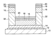
図1は、第1の実施形態に係る薄膜トランジスタ100の構成を概略的に示している。本実施形態に係る薄膜トランジスタ100は、ボトムゲート型のトップコンタクト型であり、ゲート電極12と、ゲート電極12上に形成されている絶縁層14と、絶縁層14を隔ててゲート電極12に対向する位置に形成されている酸化物半導体層16と、Ga又はAlを主成分とする酸化物を含み、酸化物半導体層16上に形成されている保護層18と、Inを主成分とする非晶質酸化物を含み、保護層18上に形成されている接触層20A,20Bと、接触層20A,20B上で、該接触層20A,20Bに接触しているとともに対向配置されているソース電極22A及びドレイン電極22Bと、を有する。接触層20A,20Bは、図1及び図2に示すように、保護層18とソース電極22A及びドレイン電極22Bとが厚さ方向で重なる領域に形成されており、ソース電極22Aとドレイン電極22Bとの間では分離している。
<First Embodiment>
FIG. 1 schematically shows a configuration of a
このような構成の薄膜トランジスタ100では、保護層18は、図1及び図3に示すように、酸化物半導体層16上に形成されているため、酸化物半導体層16は空気や酸素から保護され、製造工程中もプラズマダメージ、スパッタダメージ等から保護される。また、保護層18は、ソース電極22Aとドレイン電極22Bとの間に存在しているが、導電性が低いため、ソース電極22Aとドレイン電極22Bが保護層18を介して通電することは抑制される。
In the
一方、保護層18とソース・ドレイン電極22A,22Bとが厚さ方向で重なる領域には、導電性の接触層20A,20Bが介在しているため、オーミックコンタクトが実現される。また、ソース電極22Aとドレイン電極22Bとの間では接触層20A,20Bは分離しているため、ソース・ドレイン電極22A,22Bは接触層20A,20Bを介して通電せずに、ソース・ドレイン電極22A,22Bの間ではオフ時では高抵抗が確保される。従って、オフ電流が抑制されるとともに、オン電流は図1の矢印Aに示すように酸化物半導体層16を介して流れ、閾値変動も抑制された安定した動作特性を示すことになる。
On the other hand, since the
次に、本実施形態に係る電界効果型トランジスタの各構成について具体的に説明する。
−基板−
電界効果型トランジスタ100を支持する基板(支持体)10としては、少なくとも電界効果型トランジスタ100を形成する面が絶縁性を有し、寸法安定性、耐溶剤性、加工性、耐熱性などを有するものを用いる。また、最終製品として、例えば有機ELディスプレイを製造する場合は、水分や酸素の透過が抑制される基板を用いる。また、基板10側から光を透過させて発光や表示を行う場合は、光透過性を有する基板を用いる。
Next, each configuration of the field effect transistor according to the present embodiment will be specifically described.
-Board-
As the substrate (support) 10 for supporting the
上記のような条件を満たす基板10としては、ガラス、ジルコニア安定化酸化イットリウム(YSZ)等の無機材料が好適である。なお、ガラスからの溶出イオンを少なくするため、無アルカリガラスを用いることが好ましい。また、ソーダライムガラスを用いる場合には、シリカなどのバリアコートを施したものを使用することが好ましい。
As the
一方、基板10側から光を取り出す必要がない場合は、例えば、ステンレス、Fe、Al、Ni、Co、Cuやこれらの合金等の金属基板やSiなどの半導体基板を用い、基板10上に電気絶縁性を確保するための絶縁膜を設けてもよい。金属製の基板であれば、安価なものもあり、厚みが薄くても、強度が高く、大気中の水分や酸素に対して高いバリア性を有するものとなる。
On the other hand, when it is not necessary to extract light from the
また、有機材料からなる樹脂基板を使用してもよい。例えば、ポリエチレンテレフタレート、ポリブチレンテレフタレート、ポリエチレンナフタレート等のポリエステル、ポリスチレン、ポリカーボネート、ポリエーテルスルホン、ポリアリレート、アリルジグリコールカーボネート、ポリイミド、ポリシクロオレフィン、ノルボルネン樹脂、ポリ(クロロトリフルオロエチレン)等の合成樹脂等の有機材料などが挙げられる。 Further, a resin substrate made of an organic material may be used. For example, polyesters such as polyethylene terephthalate, polybutylene terephthalate, polyethylene naphthalate, polystyrene, polycarbonate, polyethersulfone, polyarylate, allyl diglycol carbonate, polyimide, polycycloolefin, norbornene resin, poly (chlorotrifluoroethylene), etc. Examples thereof include organic materials such as synthetic resins.
基板10の形状、構造、大きさ、厚み等については特に制限はなく、目的等に応じて適宜選択すればよい。一般的には、基板10の形状としては、取り扱い性、電界効果型トランジスタ100の形成容易性等の観点から、板状であることが好ましい。基板10の構造は、単層構造であってもよいし、積層構造であってもよい。また、基板10は、単一部材で構成されていてもよいし、2つ以上の部材で構成されていてもよい。
The shape, structure, size, thickness and the like of the
−ゲート電極−
ゲート電極12は、電圧の印加によって活性層16を介してソース・ドレイン電極22A,22B間の電流を制御する。ゲート電極12を構成する材料としては、例えば、Al、Mo、Cr、Ta、Ti、Au、またはAg等の金属、Al−Nd、APC等の合金、酸化錫、酸化亜鉛、酸化インジウム、酸化インジウム錫(ITO)、酸化亜鉛インジウム(IZO)等の金属酸化物導電膜、ポリアニリン、ポリチオフェン、ポリピロ−ルなどの有機導電性化合物、またはこれらの混合物が好適に挙げられる。
ゲート電極12の厚みは、ゲート配線の抵抗を下げ、TFTの制御信号の遅延を防ぐ観点から、10nm以上であることが好ましく、ゲート電極12の上に形成される各層の段差を小さくして破断を防止する観点から、1000nm以下であることが好ましい。
-Gate electrode-
The
The thickness of the
−絶縁層−
絶縁層(ゲート絶縁層)14はゲート電極12上に形成されている。ゲート絶縁層14は、例えばSiO2、SiNx、SiON、Al2O3、Y2O3、Ta2O5、HfO2等の絶縁体から構成され、それらの化合物を2種以上含む絶縁層としてもよい。また、ポリイミドのような高分子絶縁体を用いてもよい。
−Insulating layer−
The insulating layer (gate insulating layer) 14 is formed on the
ゲート絶縁層14の厚みは、リーク電流の抑制及び電圧耐性の向上のための厚みを有する必要がある一方、ゲート絶縁層14の厚みが大き過ぎると駆動電圧の上昇を招いてしまう。ゲート絶縁層14の材質にもよるが、成膜に要する時間と電圧耐性の観点から、ゲート絶縁層14の厚さは、無機絶縁体であれば50nm以上1000nm以下が好ましく、高分子絶縁体であれば0.5μm以上5μm以下が好ましい。
The thickness of the
−酸化物半導体層−
酸化物半導体層(活性層)16は、絶縁層14を隔ててゲート電極12に対向する位置に形成されている。酸化物半導体層16を構成する材料としては、非晶質酸化物半導体が好ましい。非晶質酸化物半導体は、低温で成膜可能であるため、プラスチックのような可撓性を有する樹脂基板にも成膜することができる。
In、Ga、Zn及びSnの少なくとも一つを含有する非晶質酸化物半導体が好ましく、In又はZnを含有する非晶質酸化物半導体がより好ましい。低温で成膜可能な非晶質酸化物半導体としては、Inを含む酸化物、InとZnを含む酸化物、及びIn、Ga及びZnを含む酸化物が挙げられ、組成構造としては、InGaO3(ZnO)m(mは6未満の自然数)のものが好ましい。これらは、キャリアが電子のn型半導体である。なお、ZnO・Rh2O3、CuGaO2、SrCu2O2のようなp型酸化物半導体を活性層16に用いてもよいし、特開2006−165529号公報に開示されている酸化物半導体を用いてもよい。
-Oxide semiconductor layer-
The oxide semiconductor layer (active layer) 16 is formed at a position facing the
An amorphous oxide semiconductor containing at least one of In, Ga, Zn, and Sn is preferable, and an amorphous oxide semiconductor containing In or Zn is more preferable. As an amorphous oxide semiconductor that can be formed at a low temperature, an oxide containing In, an oxide containing In and Zn, and an oxide containing In, Ga, and Zn can be given. As a composition structure, InGaO 3 (ZnO) m (m is a natural number less than 6) is preferred. These are n-type semiconductors whose carriers are electrons. Note that a p-type oxide semiconductor such as ZnO.Rh 2 O 3 , CuGaO 2 , or SrCu 2 O 2 may be used for the
結晶状態における組成がInGaO3(ZnO)m(mは6未満の自然数)で表される非晶質酸化物半導体が好ましく、特にInGaZnO4(適宜「IGZO」という。)がより好ましい。この組成の非晶質酸化物半導体の特徴としては、電気伝導度が増加するにつれ電子移動度が増加する傾向を示す。電気伝導度を制御するには、成膜中の酸素分圧により制御が可能である。
酸化物半導体層16の厚みは、ドレイン電流が十分に流れる観点と、成膜に要する時間が長くなり過ぎないようにする観点から、50nm以上150nm以下とすることが好ましい。
また、酸化物半導体層16の電気伝導度は、活性層として機能させるため、10−4Scm−1以上102Scm−1未満であることが好ましく、10−1Scm−1以上102Scm−1未満であることがより好ましい。
An amorphous oxide semiconductor whose composition in the crystalline state is represented by InGaO 3 (ZnO) m (m is a natural number less than 6) is preferable, and InGaZnO 4 (referred to as “IGZO” as appropriate) is particularly preferable. As a feature of the amorphous oxide semiconductor having this composition, the electron mobility tends to increase as the electrical conductivity increases. In order to control the electrical conductivity, it can be controlled by the oxygen partial pressure during film formation.
The thickness of the
Further, the electrical conductivity of the
−保護層−
保護層18は、Ga又はAlを主成分とする酸化物を含み、酸化物半導体層16上に形成されている。ここで「Ga又はAlを主成分とする酸化物」とは、保護層18を構成する酸化物が、酸素以外の構成成分のうちGa又はAlの含有量(質量比)が最も多いことを意味し、50質量%以上であることが好ましく、90質量%以上であることがより好ましい。保護層18を構成するGa又はAlを主成分とする酸化物としては具体的にはGa2O3、Al2O3など挙げられる。また、In−Ga−Zn−O系の酸化物であって、In、ZnよりもGaを多く含む(好ましくはGaが50質量%以上)Gaリッチの酸化物でもよい。なお、酸化物半導体層16として、IGZO層を形成する場合は、電気特性、親和性などの観点から、酸化ガリウム、具体的には、Ga2O3、あるいは、上記のようなGaリッチのIn−Ga−Zn−O系酸化物から保護層18を形成することが好ましい。
-Protective layer-
The
保護層18は、酸化物半導体層16上の少なくともソース・ドレイン電極22A,22Bと重なる領域とソース・ドレイン電極22A,22B間の領域に形成されていればよいが、酸化物半導体層16を効果的に保護する観点から、図3に示すように、酸化物半導体層16上の全体に形成されていることが好ましい。
The
保護層18の厚みは、ソース・ドレイン電極22A,22Bの成膜時のスパッタダメージや製造後の外気(酸素、水分)から活性層16を確実に保護する観点から10nm以上であることが好ましい。一方、保護層18は導電性が低いため、保護層18が厚過ぎると絶縁性が高くなり駆動電圧の上昇を招くおそれがある。駆動電圧の上昇を抑制する観点から、保護層18の厚みは30nm以下であることが好ましい。
また、保護層18の電気伝導度は、保護層18を介したソース・ドレイン間の通電を防ぐため、106Scm−1以上1012Scm−1未満であることが好ましく、107Scm−1以上1010Scm−1未満であることがより好ましい。
The thickness of the
The electric conductivity of the
−接触層−
接触層20A,20Bは、Inを主成分とする非晶質酸化物を含み、保護層18とソース電極22A及びドレイン電極22Bとが厚さ方向で重なる領域に形成され、ソース電極22A及びドレイン電極22Bに接触しているとともにソース電極22Aとドレイン電極22Bとの間では分離している。ここで「Inを主成分とする非晶質酸化物」とは、接触層20A,20Bを構成する酸化物が、酸素以外の構成成分のうちInの含有量(質量比)が最も多いことを意味し、75質量%以上であることが好ましく、80質量%以上であることがより好ましい。なお、本実施形態では、接触層20A,20Bは保護層18とも接触しているが、必ずしも保護層18と接触している必要はなく、保護層18と接触層20A,20Bとの間に他の層(中間層)が介在してもよい。
-Contact layer-
The contact layers 20A and 20B include an amorphous oxide containing In as a main component, and are formed in a region where the
接触層20A,20Bを構成する非晶質酸化物としては、例えば、酸化物半導体層16としてIGZO層を形成する場合は、親和性、オーミックコンタクト性などの観点から、非晶質IZO(インジウム亜鉛オキサイド)、非晶質ITO(インジウムスズオキサイド)、又は非晶質In2O3であることが好ましい。
接触層20A,20Bの厚みは、オーミックコンタクトを確実に実現する観点から10nm以上であることが好ましく、成膜に要する時間が長くなり過ぎないようにする観点から、30nm以下であることが好ましい。
また、接触層20A,20Bの電気伝導度は、オーミックコンタクトを確実に実現するため、101Scm−1以上104Scm−1未満であることが好ましく、102Scm−1以上103Scm−1未満であることがより好ましい。
As an amorphous oxide constituting the contact layers 20A and 20B, for example, when an IGZO layer is formed as the
The thickness of the contact layers 20A and 20B is preferably 10 nm or more from the viewpoint of reliably realizing ohmic contact, and is preferably 30 nm or less from the viewpoint of preventing the time required for film formation from becoming too long.
Further, the electrical conductivity of the contact layers 20A and 20B is preferably 10 1 Scm −1 or more and less than 10 4 Scm −1 in order to reliably realize ohmic contact, and is 10 2 Scm −1 or more and 10 3 Scm −. More preferably, it is less than 1 .
−ソース電極・ドレイン電極−
ソース電極22A及びドレイン電極22Bは、接触層20A,20B上で、該接触層20A,20Bに接触しているとともに対向配置されている。
ソース・ドレイン電極22A,22Bを構成する材料としては、具体的には、Al、Mo、Cr、Ta、Ti、Au、Ag等の金属、Al−Nd、APC等の合金、酸化錫、酸化亜鉛、酸化インジウム、酸化インジウム錫(ITO)、酸化亜鉛インジウム(IZO)等の金属酸化物導電膜、ポリアニリン、ポリチオフェン、ポリピロールなどの有機導電性化合物、またはこれらの混合物が挙げられる。なお、ソース・ドレイン電極22A,22BはInを主成分とする非晶質酸化物を含む接触層20A,20Bと接触するため、接触層20A,20Bとの親和性から金属、合金、又は金属酸化物導電膜から形成することが好ましい。
−Source / Drain electrode−
The source electrode 22A and the
Specifically, the materials constituting the source /
ソース電極22A及びドレイン電極22Bの厚みは、その材料、最終製品などによって異なるが、成膜性、導電性(低抵抗化)などを考慮すると、10nm以上1000nm以下とすることが好ましい。なお、ソース・ドレイン電極22A,22Bの後で活性層を形成する場合は、活性層の厚みや段差を小さくすることを考慮し、ソース・ドレイン電極22A,22Bの厚みが制限されるが、本実施形態では、活性層16等を形成した後にソース・ドレイン電極22A,22Bを形成するため、ソース・ドレイン電極22A,22Bの後で活性層16を形成する場合に比べ、ソース・ドレイン電極22A,22Bをより厚く形成して低抵抗化を図ることもできる。
The thicknesses of the
次に、本実施形態に係る薄膜トランジスタ100を製造する方法について具体的に説明する。図4〜図7は、それぞれ本実施形態に係る薄膜トランジスタ100を製造する工程を概略的に示している。
Next, a method for manufacturing the
−ゲート電極の形成−
基板10上にゲート電極12を形成する。例えば、印刷方式、コーティング方式等の湿式方式、真空蒸着法、スパッタリング法、イオンプレーティング法等の物理的方式、CVD、プラズマCVD法等の化学的方式、などの中から使用する材料との適性を考慮して適宜選択した方法に従って成膜する。
成膜後、フォトリソグラフィ法によって所定の形状にパターニングを行う。このとき、ゲート電極12及びゲート配線を同時にパターニングする。
-Formation of gate electrode-
A
After film formation, patterning is performed into a predetermined shape by photolithography. At this time, the
−ゲート絶縁層の形成−
基板10上にゲート電極12を形成した後、絶縁層(ゲート絶縁層)14を形成する。ゲート絶縁層14は、印刷方式、コーティング方式等の湿式方式、真空蒸着法、スパッタリング法、イオンプレーティング法等の物理的方式、CVD、プラズマCVD法等の化学的方式、などの中から使用する材料との適性を考慮して適宜選択した方法に従ってゲート電極12及び基板10上に成膜し、必要に応じてフォトリソグラフィ法によって所定の形状にパターニングを行う。
-Formation of gate insulation layer-
After forming the
−酸化物半導体層、保護層、及び接触層の形成−
酸化物半導体層16、保護層18、及び接触層20A,20Bを形成する方法は特に限定されないが、レジストを用いたリフトオフやエッチングにより所定のパターンに形成することができる。
例えば、ゲート絶縁層14上にリフトオフ用のレジストを塗布し、露光後、現像する。ここでは、リフトオフ用のレジストはアルカリ性の剥離液に溶解する材料を用いる。これにより、図4に示されるように、酸化物半導体層16を形成すべき箇所ではゲート絶縁層14が露出し、酸化物半導体層16を形成しない箇所ではレジスト膜が残留するようにレジストパターン32を形成する。
-Formation of oxide semiconductor layer, protective layer, and contact layer-
A method for forming the
For example, a lift-off resist is applied on the
次いで、活性層としてIGZO層16を成膜する。例えば、In、Ga、及びZnを目標の組成で含む酸化物半導体の多結晶焼結体をターゲットとして気相成膜法を用いて成膜する。気相成膜法の中でも、スパッタリング法及びパルスレーザー蒸着法(PLD法)がより好ましく、量産性の観点から、スパッタリング法が特に好ましい。
Next, an
IGZO層16を成膜した後、保護層としてGa2O3層18を、接触層としてIZO層20を順次成膜する。この場合も各層18,20に応じたターゲットを用いてスパッタリング法によりそれぞれ成膜すればよい。これにより、図5に示されるように、ゲート絶縁層14及びレジストパターン32上にIGZO層16、Ga2O3層18、及びIZO層20が積層される。
なお、各層16,18,20は、それぞれX線回折法や、高解像度断面TEM写真により結晶状態を確認することができる。また、厚さは、触針式表面形状測定や、断面TEM写真により求めることができ、組成比は、XRF(蛍光X線分析)や、XPS(X線光電子分光分析)、SIMSにより求めることができる。
After the
In addition, each
IGZO層16、Ga2O3層18、及びIZO層20を順次形成して積層した後、剥離液(アルカリ性)によりレジストパターン32を溶解させる。このとき、レジストパターン32上の各層16,18,20はレジストの溶解とともに除去されるが、絶縁層14上に形成されている各層16,18,20は、最表面のIZO層20がアルカリ溶液に対してほとんど溶解しないため、そのまま残留することになる。
After the
−ソース・ドレイン電極の形成−
次いで、ソース・ドレイン電極22A,22Bを形成する。ソース・ドレイン電極22A,22Bを形成する方法も特に限定されないが、レジストを用いたリフトオフやエッチングによりパターン形成することができる。
例えば、リフトオフ用のレジストパターン34を形成する。ここでもリフトオフ用のレジストはアルカリ性の剥離液に溶解する材料を用い、レジストを塗布し、露光後、現像する。これにより、ソース・ドレイン電極22A,22Bを形成すべき領域では、IGZO層16、Ga2O3層18、及びIZO層20の積層体24又はゲート絶縁層14を露出させ、ソース電極22Aとドレイン電極22Bを形成しない領域では、ソース・ドレイン電極22A,22B間の領域を含めてレジスト膜34を残留させる。
-Formation of source / drain electrodes-
Next, source /
For example, a resist
リフトオフ用のレジストパターン34を形成した後、図6に示すように、ソース・ドレイン電極22A,22Bを形成するための金属膜22を成膜する。成膜法は特に限定されず、印刷方式、コーティング方式等の湿式方式、真空蒸着法、スパッタリング法、イオンプレーティング法等の物理的方式、CVD、プラズマCVD法等の化学的方式などの中から材料との適性を考慮して選択した方法に従って成膜すればよい。例えば、スパッタリング法によりMo膜22を形成する。これにより、ゲート絶縁層14、積層体24、及びレジストパターン34の各露出部分にMo膜22が形成される。
なお、例えば、ソース電極22A及びドレイン電極22Bの材料としてITOを選択する場合には、直流あるいは高周波スパッタリング法、真空蒸着法、イオンプレーティング法等に従って成膜することができ、有機導電性化合物を選択する場合には湿式成膜法に従って行うことができる。
After the lift-off resist
For example, when ITO is selected as the material of the
Mo膜22を形成した後、剥離液(アルカリ性)を用いてレジストパターン34を溶解して除去する。これにより、図7に示すように、レジストパターン34上に形成されていたMo膜22はレジスト34とともに除去され、レジストパターン34から露出していた領域ではMo膜22が残留してソース・ドレイン電極22A,22Bが形成される。なお、ソース・ドレイン電極22A,22B間では剥離液によってレジストパターン34が除去された後、IZO層20が露出するが、耐アルカリ性であるため、積層体24はそのまま残留する。
After the
一方、ソース・ドレイン電極22A,22Bの形成としてエッチングを行う場合は、ドライエッチングは設備が高価であり、製造コストが上昇するため、コストの低減が可能なウエットエッチングを用いた加工が望ましい。例えば、保護層18をGa2O3ベースの非晶質酸化膜(厚さ:10nm以上)とし、接触層20をIn2O3ベースの非晶質酸化膜(厚さ:10nm以上)とすることで、酸化物半導体層16に影響を与えることなく、ウエットエッチングによるソース・ドレイン電極22A,22Bの形成を実現することができる。
On the other hand, when etching is performed as the formation of the source /
−接触層の一部除去−
次いで、ソース・ドレイン電極22A,22Bから露出しているIZO層20をエッチングにより除去する。例えば、シュウ酸等の弱酸を用いてエッチングすることで、IZO層20の露出部分は溶解して除去され、Ga2O3層18とソース・ドレイン電極22A,22Bとの間に挟まれている部分は残留する。なお、IZO層20が除去された部分では、Ga2O3層18が露出する。Ga2O3層18はアルカリ性の剥離液には溶け易いが、耐酸性であり、酸性のエッチング液に対してはエッチングストッパーとして機能してそのまま残留する。これにより、ソース・ドレイン電極22A,22Bと活性層(IZO層)20が厚さ方向で重なり合う部分(オーバーラップ領域)のみに導電性の非晶質酸化物のIZO層20が介在し、活性層20上には全体的にGa2O3層18が保護層として残留する。
-Partial removal of contact layer-
Next, the
上記のような工程を経て、図1に示すような構成を有する薄膜トランジスタ100が作製される。このような構成の薄膜トランジスタ100は、IGZO層16の上面がGa2O3層18で覆われて外気(酸素、水)から保護されるとともに、Ga2O3層18とソース・ドレイン電極22A,22Bとの間には導電性のIZO層20A,20Bが介在しているため、オーミックコンタクトが実現される。
Through the steps as described above, the
一方、ソース電極22Aとドレイン電極22Bとの間ではIZO層20A,20Bは分離し、バックチャネル上には無いので、ソース・ドレイン電極22A,22BはIZO層20A,20Bを介して通電することはなく、TFT動作に悪影響を及ぼすことはない。
また、Ga2O3層18は、IGZO層16上の全体に形成されており、ソース電極22Aとドレイン電極22Bとの間にも存在するが、導電性が低いため、Ga2O3層18を介して通電せず、オフ時にはソース・ドレイン電極間では高抵抗が維持される。従って、オン電流は、ソース・ドレイン電極22A,22Bは、図1の矢印Aに示すようにIGZO層16を介して通電し、安定した動作特性を示すことになる。
On the other hand, since the IZO layers 20A and 20B are separated between the
Further, the Ga 2 O 3 layer 18 is formed on the entire surface of the
電界効果型トランジスタ100を製造した後は、最終製品(表示装置、撮像装置など)に応じてさらに画素電極等を形成すればよい。例えば、有機ELディスプレイを製造する場合は、層間絶縁膜、画素電極等を形成し、さらに有機エレクトロルミネッセンス層及びAl等により上部電極(共通電極)を順次形成した後、ガラス等で封止する。
After the
<第2の実施形態>
図8は、第2の実施形態に係る薄膜トランジスタ200の構成を概略的に示している。本実施形態に係る薄膜トランジスタ200では、酸化物半導体層16上にはGa又はAlを主成分とする酸化物を含む保護層18が形成されている。保護層18とソース・ドレイン電極22A,22Bとの間には、Inを主成分とする非晶質酸化物を含む接触層20A,20Bが形成されており、ソース・ドレイン電極22A,22Bに接触しているとともにソース電極22Aとドレイン電極22Bとの間で分離している。さらに、保護層18と接触層20A,20Bとの間には、第1の中間層17A,17Bと、第2の中間層19A,19Bが形成されている。これらの中間層17A,17B,19A,19Bは、接触層20A,20Bと同様、厚さ方向において酸化物半導体層16とソース・ドレイン電極22A,22Bとが重なる領域に形成されており、ソース電極22Aとドレイン電極22Bとの間では分離している。従って、ソース電極22Aとドレイン電極22Bはこれらの中間層17A,17B,19A,19Bを介して通電することもない。
<Second Embodiment>
FIG. 8 schematically shows a configuration of a
このような構成の薄膜トランジスタ200も、酸化物半導体層16は保護層18で覆われているため製造工程中のダメージや外気から保護される。例えば、製造工程におけるダメージ防止効果を増すには、保護層としてGa2O3層18を形成した後、IZO層17A,17Bを厚み10nm程度で介在させてから、再びGa2O3層19A,19Bを10nm程度の厚みで積層することが効果的である。
また、保護層18とソース・ドレイン電極22A,22Bとが重なる領域では、保護層18よりも導電性の高い接触層20A,20Bがソース・ドレイン電極22A,22Bと接触しているため、オーミックコンタクトが実現される。従って、オフ時にはソース・ドレイン電極22A,22B間の高抵抗が確保され、オン時にはソース・ドレイン電極22A,22B間は図8の矢印Aに示すように酸化物半導体層16を介して通電し、閾値変動が抑制され、安定した動作特性を示すことになる。
In the
Further, in the region where the
以下、実施例を説明するが、本発明はこれらに限定されるものではない。なお、以下の説明において、括弧内の単位(nm)が付いた数値は膜厚を表している。
<実施例1>
以下の工程により図1に示す構成を有する薄膜トランジスタを製造した。
ガラス基板上にゲート電極としてスパッタリングによってMo膜(40nm)を成膜した。
次いで、ゲート絶縁層としてスパッタリングによってSiO2膜(200nm)を成膜した。
ゲート電極と対向し、ゲート絶縁層上にアイランド化した活性層を形成するため、リフトオフ用のレジスト(東京応化工業社製:TSMR8900)の塗布、パターン露光、及び現像を順次行った。
Hereinafter, examples will be described, but the present invention is not limited thereto. In the following description, the numerical value with the unit (nm) in parentheses represents the film thickness.
<Example 1>
A thin film transistor having the configuration shown in FIG. 1 was manufactured through the following steps.
A Mo film (40 nm) was formed as a gate electrode on a glass substrate by sputtering.
Next, a SiO 2 film (200 nm) was formed as a gate insulating layer by sputtering.
In order to form an islanded active layer on the gate insulating layer opposite to the gate electrode, application of a lift-off resist (manufactured by Tokyo Ohka Kogyo Co., Ltd .: TSMR8900), pattern exposure, and development were sequentially performed.
次いで、IGZO膜(50nm)/Ga2O3膜(10nm)/IZO膜(10nm)をそれぞれスパッタリングで連続成膜した。
次いで、リフトオフ用レジストをアルカリ性剥離液(AZ社製:AZリムーバ100)で剥離した後、純水でリンスした。この時、IZO膜(10nm)は消失しなかった。
Next, an IGZO film (50 nm) / Ga 2 O 3 film (10 nm) / IZO film (10 nm) were successively formed by sputtering.
Next, the lift-off resist was stripped with an alkaline stripping solution (manufactured by AZ: AZ remover 100), and then rinsed with pure water. At this time, the IZO film (10 nm) did not disappear.
ソース・ドレイン電極を一部が活性層にオーバーラップした状態となるようにリフトオフ形成するため、リフトオフ用のレジスト(東京応化工業社製:TSMR8900)の塗布、露光、及び現像を行った。
リフトオフ用のレジストパターンを形成した後、Mo膜(40nm)をベタ成膜した。
次いで、リフトオフ用レジストをアルカリ性剥離液(AZリムーバ100)で剥離し、純水でリンスした。この時、IZO膜(10nm)は消失しなかった。
さらに、シュウ酸に5分間浸漬して、バックチャネル部のIZO膜を除去した。
これにより図1に示すような構成を有する薄膜トランジスタを製造した。
得られた薄膜トランジスタはオフ電流及び閾値変動がほとんど無く、良好に動作した。なお、この時の薄膜トランジスタのゲート長は200μm、ゲート幅は1000μmであり、トランジスタの測定条件はドレイン電圧に10V固定印加し、ゲート電圧を−10Vから+15Vまで、10回走査する条件である。
In order to form a lift-off so that the source / drain electrodes partially overlap the active layer, a lift-off resist (Tokyo Ohka Kogyo Co., Ltd .: TSMR8900) was applied, exposed, and developed.
After forming a resist pattern for lift-off, a Mo film (40 nm) was formed as a solid film.
Next, the lift-off resist was stripped with an alkaline stripping solution (AZ remover 100) and rinsed with pure water. At this time, the IZO film (10 nm) did not disappear.
Further, it was immersed in oxalic acid for 5 minutes to remove the IZO film in the back channel portion.
Thus, a thin film transistor having a configuration as shown in FIG. 1 was manufactured.
The obtained thin film transistor operated satisfactorily with little off-state current and threshold fluctuation. At this time, the gate length of the thin film transistor is 200 μm, the gate width is 1000 μm, and the measurement conditions of the transistor are conditions in which a fixed voltage of 10 V is applied to the drain voltage and the gate voltage is scanned 10 times from −10 V to +15 V.
<実施例2>
以下の工程により図8に示す構成を有する薄膜トランジスタを製造した。
実施例1と同様に、ガラス基板上に、ゲート電極としてMo膜(40nm)と、ゲート絶縁層としてSiO2膜(200nm)を順次成膜した。
ゲート電極と対向し、ゲート絶縁層上にアイランド化した活性層を形成するため、リフトオフ用のレジストの塗布、パターン露光、及び現像を順次行った。
<Example 2>
A thin film transistor having the configuration shown in FIG. 8 was manufactured through the following steps.
Similarly to Example 1, a Mo film (40 nm) as a gate electrode and a SiO 2 film (200 nm) as a gate insulating layer were sequentially formed on a glass substrate.
Application of lift-off resist, pattern exposure, and development were sequentially performed in order to form an islanded active layer on the gate insulating layer facing the gate electrode.
次いで、IGZO膜(50nm)/第1のGa2O3膜(10nm)/第1のIZO膜(10nm)/第2のGa2O3膜(10nm)/第2のIZO膜(10nm)をスパッタリングで連続成膜した。 Next, IGZO film (50 nm) / first Ga 2 O 3 film (10 nm) / first IZO film (10 nm) / second Ga 2 O 3 film (10 nm) / second IZO film (10 nm) Continuous film formation was performed by sputtering.
活性層をアイランド化するため、ウエットエッチング用のレジスト(東京応化工業社製:TSMR8900)の塗布、パターン露光、及び現像を行い、レジストマスクを形成した。
次いで、Alエッチング液(関東化学(株)製;燐酸、硝酸、及び酢酸の混合液)を用いて活性層をエッチングしてパターン化した。
エッチング後、レジストをアルカリ性剥離液(AZリムーバ100)で剥離した後、純水でリンスした。この時、最表面の第2のIZO膜は残っていた。
In order to make the active layer into an island, a resist for wet etching (manufactured by Tokyo Ohka Kogyo Co., Ltd .: TSMR8900) was applied, patterned, and developed to form a resist mask.
Next, the active layer was etched and patterned using an Al etching solution (manufactured by Kanto Chemical Co., Inc .; mixed solution of phosphoric acid, nitric acid and acetic acid).
After the etching, the resist was stripped with an alkaline stripping solution (AZ remover 100) and rinsed with pure water. At this time, the second IZO film on the outermost surface remained.
次いで、ソース・ドレイン電極用のMo膜(100nm)をベタ成膜した。ソース・ドレイン電極を、一部が活性層にオーバーラップした状態となるようにウエットエッチングにより形成するため、レジストの塗布、露光、及び現像を行った後、Alエッチング液でエッチングした。最表面の第2のIZO膜は、バックチャネル領域では消失し、オーバーラップ領域では残っていた。 Next, a solid Mo film (100 nm) for source / drain electrodes was formed. In order to form the source / drain electrodes by wet etching so that a part of the source / drain electrodes overlaps the active layer, the resist was applied, exposed and developed, and then etched with an Al etching solution. The second IZO film on the outermost surface disappeared in the back channel region and remained in the overlap region.
レジストマスクをアルカリ性剥離液(AZリムーバ100)で剥離した後、純水でリンスした。この時、バックチャネル領域の第2のGa2O3膜は消失し、第1のIZO膜は残っていた。オーバーラップ領域の第2のGa2O3膜及び第1のIZO膜は残っていた。 The resist mask was stripped with an alkaline stripping solution (AZ remover 100) and rinsed with pure water. At this time, the second Ga 2 O 3 film in the back channel region disappeared and the first IZO film remained. The second Ga 2 O 3 film and the first IZO film in the overlap region remained.
この状態で、シュウ酸に3分間浸漬して、バックチャネル領域のみ第1のIZO膜を除去した。このとき、オーバーラップ領域の第2のGa2O3膜と第1のIZO膜は残っていた。
これにより図8に示すような構成を有する薄膜トランジスタを製造した。
得られた薄膜トランジスタはオフ電流及び閾値変動がほとんど無く、良好に動作した。なお、この時の薄膜トランジスタのゲート長は200μm、ゲート幅は1000μmであり、トランジスタの測定条件はドレイン電圧に10V固定印加し、ゲート電圧を−10Vから+15Vまで、10回走査する条件である。
In this state, the first IZO film was removed only in the back channel region by immersing in oxalic acid for 3 minutes. At this time, the second Ga 2 O 3 film and the first IZO film in the overlap region remained.
Thus, a thin film transistor having a configuration as shown in FIG. 8 was manufactured.
The obtained thin film transistor operated satisfactorily with little off-state current and threshold fluctuation. At this time, the gate length of the thin film transistor is 200 μm, the gate width is 1000 μm, and the measurement conditions of the transistor are conditions in which a fixed voltage of 10 V is applied to the drain voltage and the gate voltage is scanned 10 times from −10 V to +15 V.
<比較例1>
バックチャネル部のIZO膜を除去しなかった以外は実施例1と同様の処理を行うことで、接触層20A,20Bが繋がっている形態、すなわち図7に示す形態のTFTを作製した。
この場合は常にドレイン電流が流れ、TFTはオフ動作を示さなかった。
<Comparative Example 1>
Except that the IZO film in the back channel portion was not removed, the same processing as in Example 1 was performed, so that a TFT in which the contact layers 20A and 20B were connected, that is, the TFT shown in FIG. 7 was manufactured.
In this case, drain current always flowed, and the TFT did not show off operation.
以上、本発明について説明したが、本発明は上記実施形態及び比較例に限定されるものではない。
例えば、実施形態及び実施例では、保護層としては、Gaを主成分とする酸化物(Ga2O3)を含む場合について主に説明したが、Alを主成分とする酸化物(Al2O3)を含む保護層としても同様の効果が得られる。
As mentioned above, although this invention was demonstrated, this invention is not limited to the said embodiment and comparative example.
For example, in the embodiment and the example, the case where the protective layer includes an oxide containing Ga as a main component (Ga 2 O 3 ) is mainly described, but an oxide containing Al as a main component (Al 2 O) is mainly described. The same effect can be obtained as a protective layer containing 3 ).
また、実施形態及び実施例では、ボトムゲート型の薄膜トランジスタについて主に説明したが、例えば、図9に示すようにトップゲート型の薄膜トランジスタ300でもよい。この場合、基板10上に、酸化物半導体層16と、保護層18はGa又はAlを主成分とする酸化物を含む保護層18と、ソース電極22A及びドレイン電極22Bと、Inを主成分とする非晶質酸化物を含む接触層20A,20Bと、ソース電極22Aとドレイン電極22B上に一体的に形成された絶縁層14と、絶縁層14を隔てて酸化物半導体層16に対向する位置に形成されているゲート電極12と、を有する。接触層20A,20Bは、保護層18とソース電極22A及びドレイン電極22Bとの間に形成され、ソース電極22A及びドレイン電極22Bに接触しているとともにソース電極22Aとドレイン電極22Bとの間で分離している。このような構成のトップゲート型の薄膜トランジスタ300でも、活性層16は保護層18により保護されるとともに、ソース・ドレイン電極22A,22Bは接触層20A,20Bと接してオーミックコンタクトが形成される。これにより、オフ電流及び閾値変動が抑制され、安定した動作特性を示す。
In the embodiments and examples, the bottom-gate thin film transistor is mainly described. However, for example, a top-gate
10 基板
12 ゲート電極
14 絶縁層
16 酸化物半導体層(活性層)
17A,17B 第1の中間層
18 保護層
19A,19B 第2の中間層
20A ソース電極
20B ドレイン電極
22 金属膜
24 積層体
32,34 レジストパターン
100,200 電界効果型トランジスタ(ボトムゲート型)
300 電界効果型トランジスタ(トップゲート型)
10
17A, 17B First
300 Field Effect Transistor (Top Gate Type)
Claims (5)
前記ゲート電極上に形成されている絶縁層と、
前記絶縁層を隔てて前記ゲート電極に対向する位置に形成されている酸化物半導体層と、
Gaを主成分とする酸化物を含み、前記酸化物半導体層上に形成されている保護層と、
Inを主成分とする非晶質酸化物を含み、前記保護層上に形成されている接触層と、
前記接触層上で、該接触層に接触しているとともに対向配置されているソース電極及びドレイン電極と、を有し、
前記接触層が、前記保護層と前記ソース電極及び前記ドレイン電極とが厚さ方向で重なる領域に形成されており、前記ソース電極と前記ドレイン電極との間では分離している電界効果型トランジスタ。 A gate electrode;
An insulating layer formed on the gate electrode;
An oxide semiconductor layer formed at a position facing the gate electrode across the insulating layer;
A protective layer containing an oxide containing Ga as a main component and formed on the oxide semiconductor layer;
A contact layer containing an amorphous oxide mainly composed of In and formed on the protective layer;
On the contact layer, a source electrode and a drain electrode that are in contact with the contact layer and disposed opposite to each other, and
The field effect transistor, wherein the contact layer is formed in a region where the protective layer, the source electrode, and the drain electrode overlap in a thickness direction, and the source electrode and the drain electrode are separated from each other.
Gaを主成分とする酸化物を含み、前記酸化物半導体層上に形成されている保護層と、
Inを主成分とする非晶質酸化物を含み、前記保護層上に形成されている接触層と、
前記接触層上で、該接触層に接触しているとともに対向配置されているソース電極及びドレイン電極と、
前記ソース電極及び前記ドレイン電極上に一体的に形成されている絶縁層と、
前記絶縁層を隔てて前記酸化物半導体層に対向する位置に形成されているゲート電極と、を有し、
前記接触層が、前記保護層と前記ソース電極及び前記ドレイン電極とが厚さ方向で重なる領域に形成されており、前記ソース電極と前記ドレイン電極との間では分離している電界効果型トランジスタ。 An oxide semiconductor layer;
A protective layer containing an oxide containing Ga as a main component and formed on the oxide semiconductor layer;
A contact layer containing an amorphous oxide mainly composed of In and formed on the protective layer;
On the contact layer, a source electrode and a drain electrode that are in contact with the contact layer and are disposed opposite to each other, and
An insulating layer integrally formed on the source electrode and the drain electrode;
A gate electrode formed at a position facing the oxide semiconductor layer with the insulating layer interposed therebetween,
The field effect transistor, wherein the contact layer is formed in a region where the protective layer, the source electrode, and the drain electrode overlap in a thickness direction, and the source electrode and the drain electrode are separated from each other.
Priority Applications (1)
| Application Number | Priority Date | Filing Date | Title |
|---|---|---|---|
| JP2009049799A JP2010205932A (en) | 2009-03-03 | 2009-03-03 | Field effect transistor |
Applications Claiming Priority (1)
| Application Number | Priority Date | Filing Date | Title |
|---|---|---|---|
| JP2009049799A JP2010205932A (en) | 2009-03-03 | 2009-03-03 | Field effect transistor |
Publications (1)
| Publication Number | Publication Date |
|---|---|
| JP2010205932A true JP2010205932A (en) | 2010-09-16 |
Family
ID=42967141
Family Applications (1)
| Application Number | Title | Priority Date | Filing Date |
|---|---|---|---|
| JP2009049799A Pending JP2010205932A (en) | 2009-03-03 | 2009-03-03 | Field effect transistor |
Country Status (1)
| Country | Link |
|---|---|
| JP (1) | JP2010205932A (en) |
Cited By (3)
| Publication number | Priority date | Publication date | Assignee | Title |
|---|---|---|---|---|
| JP2012209557A (en) * | 2011-03-28 | 2012-10-25 | Boe Technology Group Co Ltd | Amorphous oxide thin film transistor, method for manufacturing the same, and display panel comprising the same |
| WO2013128577A1 (en) * | 2012-02-28 | 2013-09-06 | 富士通株式会社 | Semiconductor device, and production method therefor |
| KR20160013431A (en) * | 2014-07-25 | 2016-02-04 | 삼성디스플레이 주식회사 | Thin film transsistor substrate and method for fabricating the same |
-
2009
- 2009-03-03 JP JP2009049799A patent/JP2010205932A/en active Pending
Cited By (6)
| Publication number | Priority date | Publication date | Assignee | Title |
|---|---|---|---|---|
| JP2012209557A (en) * | 2011-03-28 | 2012-10-25 | Boe Technology Group Co Ltd | Amorphous oxide thin film transistor, method for manufacturing the same, and display panel comprising the same |
| US9608127B2 (en) | 2011-03-28 | 2017-03-28 | Boe Technology Group Co., Ltd. | Amorphous oxide thin film transistor, method for manufacturing the same, and display panel |
| WO2013128577A1 (en) * | 2012-02-28 | 2013-09-06 | 富士通株式会社 | Semiconductor device, and production method therefor |
| JPWO2013128577A1 (en) * | 2012-02-28 | 2015-07-30 | 富士通株式会社 | Semiconductor device and manufacturing method thereof |
| KR20160013431A (en) * | 2014-07-25 | 2016-02-04 | 삼성디스플레이 주식회사 | Thin film transsistor substrate and method for fabricating the same |
| KR102230619B1 (en) * | 2014-07-25 | 2021-03-24 | 삼성디스플레이 주식회사 | Thin film transsistor substrate and method for fabricating the same |
Similar Documents
| Publication | Publication Date | Title |
|---|---|---|
| US8822988B2 (en) | Thin-film transistor (TFT) with a bi-layer channel | |
| JP5305630B2 (en) | Manufacturing method of bottom gate type thin film transistor and manufacturing method of display device | |
| JP5345349B2 (en) | Thin film field effect transistor | |
| US8143678B2 (en) | Thin film transistors having multi-layer channel | |
| JP5371467B2 (en) | FIELD EFFECT TRANSISTOR AND METHOD FOR MANUFACTURING FIELD EFFECT TRANSISTOR | |
| JP5322530B2 (en) | Thin film field effect transistor manufacturing method and thin film field effect transistor manufactured by the manufacturing method | |
| JP2010205923A (en) | Method of manufacturing field effect transistor | |
| US9659967B2 (en) | Thin-film transistor and display device having the same | |
| US9768322B2 (en) | Metal oxide TFT with improved source/drain contacts and reliability | |
| US10204973B2 (en) | Display device and thin-film transistors substrate | |
| JP2011071476A (en) | Thin film transistor, display device using the same, and method of manufacturing thin film transistor | |
| JP2007201366A (en) | Field effect transistor | |
| KR20110100580A (en) | Thin film transistor, method of manufacturing the thin film transistor, and display device | |
| US8633479B2 (en) | Display device with metal oxidel layer and method for manufacturing the same | |
| US20130260497A1 (en) | Method for manufacturing a thin film transistor array panel | |
| US20220140114A1 (en) | Method for manufacturing oxide semiconductor thin film transistor | |
| KR20140144388A (en) | Thin film transistor array panel | |
| JP2017139445A (en) | Semiconductor device and semiconductor device manufacturing method | |
| KR20110080118A (en) | Thin film transistor having etch stop multi-layers and method of manufacturing the same | |
| JP2010205932A (en) | Field effect transistor | |
| US20180190823A1 (en) | Semiconductor device and manufacturing method of semiconductor device | |
| JP6209918B2 (en) | THIN FILM TRANSISTOR AND METHOD FOR MANUFACTURING THIN FILM TRANSISTOR | |
| CN110808289A (en) | Top gate Schottky oxide thin film transistor and preparation method thereof | |
| US20150108468A1 (en) | Thin film transistor and method of manufacturing the same | |
| US10164118B2 (en) | Semiconductor device and method for producing same |