JP2010200310A - Multiband matching circuit, and multiband power amplifier - Google Patents
Multiband matching circuit, and multiband power amplifier Download PDFInfo
- Publication number
- JP2010200310A JP2010200310A JP2010006885A JP2010006885A JP2010200310A JP 2010200310 A JP2010200310 A JP 2010200310A JP 2010006885 A JP2010006885 A JP 2010006885A JP 2010006885 A JP2010006885 A JP 2010006885A JP 2010200310 A JP2010200310 A JP 2010200310A
- Authority
- JP
- Japan
- Prior art keywords
- matching
- circuit
- impedance
- parallel
- multiband
- Prior art date
- Legal status (The legal status is an assumption and is not a legal conclusion. Google has not performed a legal analysis and makes no representation as to the accuracy of the status listed.)
- Granted
Links
Images


Classifications
-
- H—ELECTRICITY
- H03—ELECTRONIC CIRCUITRY
- H03H—IMPEDANCE NETWORKS, e.g. RESONANT CIRCUITS; RESONATORS
- H03H7/00—Multiple-port networks comprising only passive electrical elements as network components
- H03H7/38—Impedance-matching networks
- H03H7/383—Impedance-matching networks comprising distributed impedance elements together with lumped impedance elements
-
- H—ELECTRICITY
- H03—ELECTRONIC CIRCUITRY
- H03F—AMPLIFIERS
- H03F1/00—Details of amplifiers with only discharge tubes, only semiconductor devices or only unspecified devices as amplifying elements
- H03F1/56—Modifications of input or output impedances, not otherwise provided for
-
- H—ELECTRICITY
- H03—ELECTRONIC CIRCUITRY
- H03F—AMPLIFIERS
- H03F3/00—Amplifiers with only discharge tubes or only semiconductor devices as amplifying elements
- H03F3/72—Gated amplifiers, i.e. amplifiers which are rendered operative or inoperative by means of a control signal
-
- H—ELECTRICITY
- H03—ELECTRONIC CIRCUITRY
- H03H—IMPEDANCE NETWORKS, e.g. RESONANT CIRCUITS; RESONATORS
- H03H7/00—Multiple-port networks comprising only passive electrical elements as network components
- H03H7/38—Impedance-matching networks
- H03H7/40—Automatic matching of load impedance to source impedance
-
- H—ELECTRICITY
- H03—ELECTRONIC CIRCUITRY
- H03F—AMPLIFIERS
- H03F2200/00—Indexing scheme relating to amplifiers
- H03F2200/111—Indexing scheme relating to amplifiers the amplifier being a dual or triple band amplifier, e.g. 900 and 1800 MHz, e.g. switched or not switched, simultaneously or not
-
- H—ELECTRICITY
- H03—ELECTRONIC CIRCUITRY
- H03F—AMPLIFIERS
- H03F2200/00—Indexing scheme relating to amplifiers
- H03F2200/429—Two or more amplifiers or one amplifier with filters for different frequency bands are coupled in parallel at the input or output
-
- H—ELECTRICITY
- H03—ELECTRONIC CIRCUITRY
- H03F—AMPLIFIERS
- H03F2203/00—Indexing scheme relating to amplifiers with only discharge tubes or only semiconductor devices as amplifying elements covered by H03F3/00
- H03F2203/72—Indexing scheme relating to gated amplifiers, i.e. amplifiers which are rendered operative or inoperative by means of a control signal
- H03F2203/7209—Indexing scheme relating to gated amplifiers, i.e. amplifiers which are rendered operative or inoperative by means of a control signal the gated amplifier being switched from a first band to a second band
-
- H—ELECTRICITY
- H03—ELECTRONIC CIRCUITRY
- H03H—IMPEDANCE NETWORKS, e.g. RESONANT CIRCUITS; RESONATORS
- H03H7/00—Multiple-port networks comprising only passive electrical elements as network components
- H03H7/38—Impedance-matching networks
- H03H2007/386—Multiple band impedance matching
Landscapes
- Engineering & Computer Science (AREA)
- Power Engineering (AREA)
- Amplifiers (AREA)
- Microwave Amplifiers (AREA)
Abstract
Description
本発明は、増幅器などに利用される整合回路及び電力増幅器に関する。より詳しくは、増幅素子など周波数特性を有する回路素子の入出力インピーダンスと周辺回路のインピーダンスとを複数の周波数帯域で同時に整合することができるマルチバンド整合回路、および当該マルチバンド整合回路を備えるマルチバンド電力増幅器に関する。 The present invention relates to a matching circuit and a power amplifier used for an amplifier and the like. More specifically, a multiband matching circuit capable of simultaneously matching input / output impedances of circuit elements having frequency characteristics such as amplifier elements and impedances of peripheral circuits in a plurality of frequency bands, and a multiband including the multiband matching circuit The present invention relates to a power amplifier.
近年、無線通信によって提供されるサービスの多様化に伴い、無線機には複数の周波数帯域の信号を扱えること(マルチバンド化)が要求されている。例えば、無線LANの規格であるIEEE802.11a/b/gの各規格では、5.2GHz帯及び2.4GHz帯の2つの周波数帯が規定されている。 In recent years, with the diversification of services provided by wireless communication, wireless devices are required to be able to handle signals in a plurality of frequency bands (multiband). For example, each standard of IEEE802.11a / b / g, which is a wireless LAN standard, defines two frequency bands, a 5.2 GHz band and a 2.4 GHz band.
無線機には、無線周波数帯の信号を増幅しアンテナに供給する電力増幅器が搭載されている。電力増幅器は、消費電力が大きい装置であることから、高効率動作を行うことが要求される。この要求を満たすには、動作周波数帯において効率に対して最適化された整合回路を設ける必要があり、異なる2つの周波数帯の双方で効率を最適化したい場合には、通常、各周波数帯に対して最適に設計された回路をスイッチによって切り替えるなどの構成がとられている。 The wireless device is equipped with a power amplifier that amplifies a signal in a radio frequency band and supplies the signal to an antenna. Since the power amplifier is a device that consumes a large amount of power, it is required to perform a highly efficient operation. In order to satisfy this requirement, it is necessary to provide a matching circuit optimized for efficiency in the operating frequency band. When it is desired to optimize efficiency in both two different frequency bands, each frequency band is usually On the other hand, a configuration is adopted in which an optimally designed circuit is switched by a switch.
図13は、非特許文献1などで開示されている2つの周波数帯の各信号を増幅可能なデュアルバンド電力増幅器300の構成の一例であり、5.2GHz帯専用に設計された5.2GHz帯増幅器10と2.4GHz帯専用に設計された2.4GHz帯増幅器20とを、2個の1入力2出力のSPDT(single-pole double-throw)スイッチ30を用いて動作周波数に応じて切り替える構成となっている。
FIG. 13 is an example of a configuration of a dual-
図13のデュアルバンド電力増幅器300を構成する各周波数帯用増幅器10、20は、それぞれ、図14に示すように入力側整合回路41、増幅素子60、出力側整合回路42から構成される。増幅器の性能は、増幅素子自体の特性と整合回路の特性とにより決定されるため、各周波数帯用増幅器10、20の増幅素子60の両端に接続される各整合回路41、42は、各々の周波数帯で整合がとれるように最適化される。図13のデュアルバンド電力増幅器300は、そのように最適化された整合回路を用いて構成した各周波数帯用増幅器10、20を、動作周波数帯に応じてSPDTスイッチ30で切り替えるため、SPDTスイッチの挿入損失が十分小さければ各増幅器は高出力、高効率に動作する。
Each of the
以上のようなデュアルバンド電力増幅器では、増幅素子が周波数特性のあるインピーダンスを有するため、使用周波数帯に応じた整合回路と組み合わせる必要から、第1の周波数帯用と第2の周波数帯用の2系統の増幅器を設ける必要がある。そのため、増幅素子や入出力整合回路など部品点数が多くなり、装置が大型化するのみならず各部品での電力消費により回路全体での消費電力が大きくなるという問題がある。また、SPDTスイッチの挿入損失により、出力電力が低下し効率が低下するという問題も生じる。更には、2つの周波数帯の混合信号を各周波数帯で同時に高効率に増幅する場合には、分配器及び合成器が必要となり、回路規模が増大するという問題もある(例えば、特表2003−504929号公報 参照)。
In the dual-band power amplifier as described above, since the amplifying element has an impedance with frequency characteristics, it is necessary to combine with a matching circuit corresponding to the used frequency band. Therefore, for the first frequency band and the
本発明の目的は、複数の周波数帯で同時に整合可能な整合回路を実現し、よって、増幅器を周波数帯ごとに複数設けることなく、単体で複数の周波数帯の混合信号を同時に増幅可能なマルチバンド電力増幅器を実現することにある。 An object of the present invention is to realize a matching circuit capable of simultaneously matching in a plurality of frequency bands, and thus, a multiband capable of simultaneously amplifying a mixed signal of a plurality of frequency bands by itself without providing a plurality of amplifiers for each frequency band. To realize a power amplifier.
本発明のマルチバンド電力増幅器は、増幅素子と本発明のマルチバンド整合回路とを備える。 The multiband power amplifier of the present invention includes an amplifying element and the multiband matching circuit of the present invention.
本発明のマルチバンド整合回路は、第1整合部と第2整合部とからなり、周波数特性のあるインピーダンスZI(f)を有する回路素子と、予め定められたインピーダンスZ0を有する回路(以下、「系の回路」という。)との間の信号経路に挿入されて、2つの周波数帯域において同時に回路素子のインピーダンスZI(f)を系の回路のインピーダンスZ0に整合する。 The multiband matching circuit of the present invention includes a circuit element having an impedance Z I (f) having a frequency characteristic, and a circuit having a predetermined impedance Z 0 (hereinafter, referred to as a first matching section and a second matching section). The impedance Z I (f) of the circuit element is simultaneously matched with the impedance Z 0 of the system circuit in the two frequency bands.
第1整合部は、一端が上記回路素子に接続され、第1の周波数帯域におけるインピーダンスをZ0に変換する。 The first matching unit is connected at one end to the circuit element and converts the impedance at the first frequency band to Z 0.
第2整合部は、一端が上記第1整合部の他端に接続され、他端が上記系の回路に接続され、特性インピーダンスが系の回路のインピーダンスZ0に等しい伝送線路や少なくとも第1の周波数帯域で上記伝送線路に等価な回路である直列整合手段と、一端が上記直列整合手段の他端で上記信号経路に接続され、他端が接地される並列整合手段と、からなる。 The second matching unit has one end connected to the other end of the first matching unit and the other end is connected to the system circuit, equal transmission line characteristic impedance is the impedance Z 0 of the circuit of the system and at least a first A series matching means that is a circuit equivalent to the transmission line in a frequency band, and a parallel matching means having one end connected to the signal path at the other end of the series matching means and the other end grounded.
また、上記並列整合手段は、上記第1の周波数帯域において上記信号経路との接続点がインピーダンス開放状態となるように構成される。そして、上記直列整合手段及び上記並列整合手段を適宜設計することにより第2の周波数帯域におけるインピーダンスをZ0に整合する。 The parallel matching means is configured such that a connection point with the signal path is in an impedance open state in the first frequency band. Then, the impedance in the second frequency band is matched with Z 0 by appropriately designing the series matching means and the parallel matching means.
本発明により、複数の周波数帯で同時に整合可能な整合回路を実現することができ、よって、増幅器を複数設けることなく、単体で複数の周波数帯の混合信号を同時に増幅可能なマルチバンド電力増幅器を実現することができる。 According to the present invention, it is possible to realize a matching circuit capable of matching simultaneously in a plurality of frequency bands. Therefore, a multiband power amplifier capable of simultaneously amplifying mixed signals in a plurality of frequency bands by itself without providing a plurality of amplifiers. Can be realized.
以下、本発明の実施の形態について、詳細に説明する。 Hereinafter, embodiments of the present invention will be described in detail.
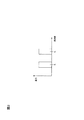
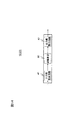
実施例1の整合回路100を図1に示す。整合回路100は、図2に示すような中心周波数をf1、f2とする2つの周波数帯域b1、b2の信号に対する整合回路である。整合回路100は、周波数特性のあるインピーダンスZI(f)を有する増幅素子60と、予め定められたインピーダンスZ0(例えば50Ω、75Ω等)を有する系の回路50との間の信号経路に挿入される。そして整合回路100は、b1、b2に対して増幅素子60のインピーダンスZI(f)を系の回路50のインピーダンスZ0に整合させる。
FIG. 1 shows a
整合回路100は、第1整合部110と第2整合部120とから構成され、第2整合部120は直列整合手段121と並列整合手段122とから構成される。
The
第1整合部110は、一端が増幅素子60に接続され、増幅素子60の第1の周波数帯域b1におけるインピーダンスZI(f1)を、他端(図1のA点)から見てZ0となるようにインピーダンス変換する。第1整合部110の構成は任意であり、例えば、伝送線路とスタブによる構成、直列インダクタと並列キャパシタによる構成等が考えられる。なお、増幅素子60のb2におけるインピーダンスZI(f2)については、ここで一旦Z(f2)に変換される。
One end of the
第1整合部110の他端には直列整合手段121の一端が接続され、直列整合手段121の他端は、系の回路50に接続される。直列整合手段121は、特性インピーダンスがZ0の伝送線路や少なくともb1において上記伝送線路と等価な遅延回路により構成される。少なくともb1における特性インピーダンスがZ0に等しい回路の構成例を、図15A、図16Aに示す。ここで、Z1、Z2は純虚数とする。Z1、Z2がb1において図15Aでは、
One end of the

の関係を、図16Aでは、 The relationship of FIG.
の関係をもつ場合、それぞれb1での整合には影響を与えない。図15A、図16Aに示す構成を用いることで、第1整合部110で変換されたb1における整合状態は上記の遅延回路の遅延量にかかわらず維持される。ここで、Z1、Z2はこれらの関係が規定されているだけであり、インダクタやキャパシタ、またはそれと同様な特性を有する分布定数回路または回路素子群等、具体的な構成は適宜選択できる。従って、各素子値をb2におけるインピーダンスの整合をとるために適宜設定することも可能となる。一方、直列整合手段121を伝送線路で構成した場合には、遅延量に関わらずb1での整合は維持される。そのため、伝送線路の遅延量は任意に設定でき、この遅延量をb2におけるインピーダンスの整合をとるために用いることができる。図15Aの具体例として、図15Bと図15Cを示す。また、図16Aの具体例として図16Bと図16Cを示す。また、これらの直列接続またはそれに相当する回路により同様な効果が得られる。
If with the relationship does not affect the integrity of each b 1. By using the configuration shown in FIGS. 15A and 16A, the matching state in b 1 converted by the
第1整合部110と直列整合手段121は、系の回路50と増幅素子60とを結ぶ信号経路上に直列に設けられる。一方、並列整合手段122はその信号経路から枝分かれする形で、系の回路50や回路素子60と並列に設けられる。
The
並列整合手段122は、一端が直列整合手段121の他端で信号経路に接続され、他端は接地される。並列整合手段122はb2のインピーダンス整合を行うため、適宜リアクタンス値を設定し、インピーダンスを調整する機能を担う。しかし、並列整合手段122は、第1整合部110で変換されたb1におけるインピーダンスZ0に影響を与えるものであってはならない。このような機能、要件を満たすべく、並列整合手段122は2つのブロックの直列接続により構成する。第1並列ブロック122aは、b1の信号に対し並列整合手段122を信号経路から切り離すためのスイッチの役割をなすブロックである。また、第2並列ブロック122bは、b2におけるインピーダンス変換に際し、適切なリアクタンス値を設定するためのブロックである。なお、第2並列ブロック122bは、先端開放線路を用い容量性のリアクタンスブロックとして構成しても構わない。
One end of the parallel matching means 122 is connected to the signal path at the other end of the series matching means 121, and the other end is grounded. The
第1並列ブロック122aは、b1において信号経路との接続点がインピーダンス開放状態(=接続点から並列整合手段122側を見たインピーダンスが無限大又はb1での整合に影響を与えない程度に大)となるように設計する。このようにインピーダンス開放状態を作ることにより、スイッチ素子を用いてON/OFFすることなく、並列整合手段122が信号経路から切り離されていると考えることができる。b1におけるインピーダンス開放状態の作り方としては、例えば、共振周波数がf1に等しいキャパシタCとインダクタLからなる並列共振回路で構成する等の方法が考えられるが、その他の任意の方法で構成して構わない。第1並列ブロック122aを並列共振回路で構成し、第2並列ブロック122bを先端開放線路で構成した場合のブロック図を図17に示す。なお、第1並列ブロック122aを並列共振回路で構成する場合、f1とCとLとの関係は次式のようになる。
The first
![]()
![]()
一方、b2においては、並列整合手段122は特定のリアクタンスとして存在する状態となり、第1並列ブロック122aと第2並列ブロック122bとが一体として並列整合手段122を構成する。並列整合手段122は、b2におけるインピーダンス変換のためのリアクタンス値の設定機能を担う。第1並列ブロック122aをキャパシタとインダクタによる並列回路で構成した場合には、f2におけるリアクタンスZLCは次式のようになる。
On the other hand, in b 2, the
![]()
![]()
そのため、第1並列ブロック122aを並列共振回路で構成した場合には、式(3)を満たし、かつ、式(4)のZLCがb2におけるインピーダンスの整合に必要なリアクタンスとなるCとLを設定すれば、第2並列ブロック122bは不要となり、図18に示すように第1並列整合手段122を第1並列ブロック122aのみで構成することができる。
Therefore, when the first
また、第1並列ブロック122aは、図19に示すようにf1の波長λ1の1/4波長の長さの伝送線路122as1とL、Cからなる共振周波数がf1である直列共振器との組み合わせにより構成することもできる。この構成ではb1において、伝送線路122as1の直列共振器が接続された一端がインピーダンス短絡状態になるため第2並列ブロック122bの構成にかかわらず、伝送線路122as1の他端がインピーダンス開放状態になり、よって並列整合手段122が回路から切り離されていると考えることができる。一方、b2において、直列共振器は特定のリアクタンスとして存在する状態となる。その結果、第1並列ブロック122aと第2並列ブロック122bとが一体として並列整合手段122を構成し、特定のリアクタンスとして存在する状態となる。そして、並列整合手段122は直列整合手段121とともにb2におけるインピーダンス変換のためのリアクタンス値の設定機能を担う。
The first
なお、第1並列ブロック122aと第2並列ブロック122bは、図1においては第1並列ブロック122aを信号経路側に、第2並列ブロック122bを接地側に配しているが、この並びは逆でも構わない。ただし、逆にする場合には、b1でのインピーダンス開放部分が両ブロックの接続点に発生するため、信号経路に接続された第2並列ブロック122bが、b1におけるインピーダンスの整合状態に影響を与えてしまうおそれがある。そこで、そのような場合には第2並列ブロック122bを集中定数素子により構成することで影響を低減できる。これにより、信号経路との接続点をb1でのインピーダンス開放状態とみなすことができ、並列整合手段122が信号経路から切り離されていると考えることができる。また、このように第1並列ブロック122aが接地側にある場合は、第1並列ブロック122aをf1における波長の4分の1の長さの伝送線路で構成することによってインピーダンス開放状態を作っても構わない。この場合、伝送線路のインピーダンスは任意であり、このインピーダンスをこのインピーダンスをb2におけるインピーダンス整合のための設計パラメータとして用いてもよい。
In FIG. 1, the first
以上のように各整合部を構成することで、b1については第1整合部110でZ0にインピーダンス変換された状態がそのまま維持されて、P1においてZ0に整合することができ、b2については第1整合部110でZ0でないZ(f2)に一旦変換されるが、いかなるZ(f2)であっても、直列整合手段121と並列整合手段122とを適宜設計することにより、P1においてZ0に整合することができる。
By configuring each matching section as described above, for b 1 is maintained a state in which the impedance conversion to Z 0 at the
そして、物理的スイッチによる切り替えを行うことなく自動的に、b1に対しては並列整合手段122が信号経路から切り離された状態で、b2に対しては並列整合手段122が信号経路に接続された状態となる。そのため、上記のような設計をすることで、2つの周波数帯の信号が同時に入力された場合でも同時に整合をとることができる。また、物理的なスイッチを用いた場合に生じるスイッチのON抵抗による損失がない低損失なマルチバンド整合回路を実現することができる。
Then, automatically without switching by physical switch, with the
なお、整合回路100を構成する各部、各手段、及び各ブロックは、それぞれが担う機能を実現可能な限り、分布定数線路、素子、若しくはこれらの組み合わせ、又は、複数の分布定数線路、複数の素子、若しくはこれらの組み合わせにより構成して構わない。素子は、抵抗(可変抵抗を含む)、キャパシタ(可変キャパシタを含む)、インダクタ(可変インダクタを含む)のような線形素子やダイオードなどの非線形二端子素子など、格別の限定は無い。
In addition, each part, each means, and each block constituting the
また、f1とf2との大小関係は問わないが、f1>f2とするのが望ましい。これはこのように構成した方が帯域幅を十分に確保しやすいこと、並列共振回路を構成する各インダクタやキャパシタの素子値が小さく済むこと、また、例えば第1並列ブロック122aを伝送線路とする場合には、高い方の周波数をf1とした方が線路長を短くできることなどの理由からである。
Further, the magnitude relationship between f 1 and f 2 does not matter, but it is desirable that f 1 > f 2 . This is because it is easy to secure a sufficient bandwidth in this way, the element values of each inductor and capacitor constituting the parallel resonant circuit can be small, and the first
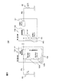
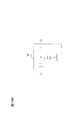
[変形例]
実施例1の変形例である整合回路150を図3に示す。整合回路150は、実施例1の第1整合部110に、参考文献1で開示されたデュアルバンド整合回路を適用し、例えば図4に示すような中心周波数をf1、f2、f3とする3つの周波数帯の信号のうち、f1とf3の組又はf2とf3の組のいずれかを選択して、選択した周波数帯の組を同時に整合可能とする整合回路である。
〔参考文献1〕福田敦史他、「MEMSスイッチを用いたマルチバンド電力増幅器」、電子情報通信学会総合大会、2004年、C-2-4、p.39
[Modification]
A
[Reference 1] Atsushi Fukuda et al., “Multiband Power Amplifiers Using MEMS Switches”, IEICE General Conference, 2004, C-2-4, p.39
第1整合部110は、主整合ブロック151と遅延回路152とスイッチ153と副整合ブロック154とから構成され、増幅素子60のb1におけるインピーダンスZI(f1)とb2におけるインピーダンスZI(f2)を、スイッチ153の切り替えにより選択的にZ0に変換する。この原理について簡単に説明する。遅延回路152は、b1での特性インピーダンスがZ0である伝送線路等により構成される。b1においては、主整合ブロック151はインピーダンスをZI(f1)からZ0に変換する。そして、遅延回路152の特性インピーダンスがZ0であるため、スイッチ153がOFF状態において点AでZ0に整合することができる。一方、b2においては、主整合ブロック151はインピーダンスをZI(f2)からZ0でないZ (f2)に変換する。そして、遅延回路152の遅延量と副整合ブロック154のリアクタンス値を適宜設定することで、スイッチ153がON状態において、いかなるZ (f2)であってもP1でZ0に整合することができる。以上のような原理の下、図3のA点からP2側を見たb1におけるインピーダンスはスイッチ153のOFF状態時にZ0となり、b2におけるインピーダンスはスイッチ153のON状態時にZ0となる。一方、第3の周波数帯域b3(中心周波数f3)におけるインピーダンスはOFF状態時にはZ(f3)に、ON状態時にはZ´(f3)に変換される。
The
第2整合部120は、第1整合部110でスイッチ153の状態に応じてb1又はb2のいずれかについてとられた整合状態(インピーダンスZ0)がP1においても維持され、かつ、b3についてP1からP2側を見たインピーダンスがZ0になるようにすることができる構成である必要がある。そこで、以下のように構成する。
In the
直列整合手段121は、b1、b2における整合状態を損なわないよう、特性インピーダンスがZ0の伝送線路や少なくともb1及びb2において上記伝送線路と等価な回路による遅延回路により構成する。少なくともb1、b2において上記伝送線路と等価な回路の構成例を図20A、図21Aに示す。ここで、Z1、Z2が少なくともb1及びb2のそれぞれにおいて、図20Aでは式(1)を図21Aでは式(2)を満たすように可変素子を調整する。図20Aの具体例として、図20Bと図20Cを示す。また、図21Aの具体例として、図21Bと図21Cを示す。また、これらの直列接続またはそれに相当する回路により同様な効果が得られる。ここで、可変インダクタは製造上困難を伴うことが多い。しかし、シャントインダクタであれば可変キャパシタを用いて可変インダクタを構成できる。図22A及び図22Bに、図20C及び図21Bの可変インダクタをそれぞれ可変キャパシタを用いて構成した例を示す。図22Aでは、一端が接地されたインダクタンスLのインダクタと容量Cのキャパシタとの直列接続は直列共振器を構成し、その共振周波数は第nの周波数帯域bnの中心周波数fnとなるように設計する。このとき、直列共振器の他端はfnでインピーダンス短絡状態となり、シャントインダクタのインダクタンスはL1となる。一方、その他の周波数では、直列共振器の他端はインピーダンス短絡状態とならず、シャントインダクタのインダクタンスをL1+L2とすることができる。また、直列共振器を構成するキャパシタを可変キャパシタとすることで、fnを可変とすることができる。さらに多くの直列共振器を用いることで、より多くのインダクタンスに対応できる。加えて、インダクタンスLのインダクタと可変キャパシタとの直列接続を無限大でないリアクタンス素子とし、シャントインダクタと一体としてZ1を構成することもできる。図22Bでは、シャントインダクタに一端が接地された容量Cのキャパシタが接続されている。シャントインダクタの一部であるインダクタンスLのインダクタと容量Cのキャパシタとの直列接続は直列共振器を構成し、その共振周波数はfnとなるように設計する。このとき、シャントインダクタと直列共振器の接続部はfnでインピーダンス短絡状態となり、シャントインダクタのインダクタンスはL1となる。一方、その他の周波数では、インピーダンス短絡状態となる位置は異なるため、周波数ごとにシャントインダクタのインダクタンスを変更することができる。また、キャパシタを可変キャパシタとすることでより多くのインダクタンスに対応できる。加えて、インダクタンスLのインダクタと可変キャパシタとの直列接続を無限大でないリアクタンス素子とし、シャントインダクタと一体としてZ1を構成することもできる。シャントインダクタの可変化については、同様なシャントリアクタンスを用いる他の実施例についても適用できる。よって、上記の実施例について、シャント可変インダクタを用いることなく、可変キャパシタのみを用いた構成が可能となる。また、図22Cのように図21Aの各素子をインダクタとキャパシタの直列接続や並列接続で構成してもよい。これらの素子の並列接続は共振周波数を境にして、周波数に応じて誘導性と容量性のリアクタンスをそれぞれ取りえる。従って、b1、b2において、それぞれ所望のリアクタンスとなるように設計することで、各周波数において式(2)を満たすことができる。ここで、図22Cは一例であり、同様な考え方に基づき、さまざまなバリエーションが考えられる。また、これらの各素子に可変デバイスを用いることで、さらに多くのバリエーションが考えられる。
第1並列ブロック122aは、b1及びb2において信号経路との接続点がインピーダンス開放状態となるように設計する。例えば、可変キャパシタとインダクタの並列回路で構成してキャパシタの容量をスイッチの状態に応じて変化させ、スイッチ153がOFF状態の時はf1で共振し、スイッチ153がON状態の時はf2で共振するようにする方法が考えられる。また、共振周波数がf2以上でf1以下である固定キャパシタとインダクタの並列回路により構成する方法も考えられる。更に、図5に示すような各周波数帯域に対応する固定キャパシタとインダクタの並列共振回路122a1、122a2を直列接続する構成や図23、24に示すようなb1についての並列共振回路122a1とそれにインダクタ又はキャパシタを付加したb2についての共振回路122a2とからなる構成によっても、各周波数帯域においてインピーダンス開放状態を実現することができる。また、図5の構成において、並列共振回路122a1の信号経路側や並列共振回路122a1と並列共振回路122a2との間に伝送線路を挿入すれば、その長さを適宜設定することで、その伝送線路をb1、b2での整合に用いることができる。図6は、図5の構成において122a1が2.6GHzで共振する並列共振回路であり、122a2が1.5GHzで共振する並列共振回路である場合の周波数−インピーダンス特性を示す図である。実線は並列共振回路122a1の特性であり、点線は並列共振回路122a1と並列共振回路122a2とを直列に接続したときの特性である。図6の点線から、これら2つの周波数帯域においてインピーダンス開放状態を実現できることがわかる。なお、図5ではキャパシタとインダクタの並列共振回路を2段構成にしているが、キャパシタかインダクタのいずれか一方又は双方に可変のものを用いることで1段で構成することも可能である。
更に、第1並列ブロック122aは、図25に示すようにf1の波長λ1の1/4波長の長さの伝送線路122as1とL1、C1からなる共振周波数がf1である直列共振器との組み合わせと、及びb2において伝送線路122as1とのセットでf2の波長λ2の1/4波長となる長さの伝送線路122as2とL2、C2からなる共振周波数がf2である直列共振器との組み合わせとにより構成することもできる。この構成ではb1において、伝送線路122as1のL1、C1からなる直列共振器が接続された一端がインピーダンス短絡状態になるため、伝送線路122as1の他端がインピーダンス開放状態になり、よって並列整合手段122が回路から切り離されていると考えることができる。b2においては、伝送線路122as2のL2、C2からなる直列共振器が接続された一端がインピーダンス短絡状態になるため、伝送線路122as2と一体として波長λ2の1/4波長線路を構成する伝送線路122as1の信号経路側端がインピーダンス開放状態になり、よって並列整合手段122が回路から切り離されていると考えることができる。一方、b3においては並列整合手段122は特定のリアクタンスとして存在する状態となり、第1並列ブロック122aと第2並列ブロック122bとが一体として並列整合手段122を構成し、b3におけるインピーダンス変換のためのリアクタンス値の設定機能を担う。図25に示す構成は、整合バンド数を増加させる場合にも同様に適用することができる。また、伝送線路122as1、122as2は、長さを調整することによりb1、b2の整合に用いることもできる。一方、b3においては、信号経路に特定のリアクタンスが接続された状態となり、具体的には第1並列ブロック122aと第2並列ブロック122bとが一体として並列整合手段122を構成して、b3におけるインピーダンス変換のためのリアクタンス値の設定機能を担う。
The first
Furthermore, the first
ただし、ここで整合対象となるインピーダンスはスイッチ153がOFF状態時にはZ(f3)、ON状態時にはZ´(f3)というように異なっているため、Z(f3)とZ´(f3)とが大きく異なっている場合には、例えば直列整合手段121に図20Aや図21Aの構成を適用したり、第2並列ブロック122bについてもリアクタンス値が可変なものとして構成し、スイッチ153の状態に応じてリアクタンス値を変化させることが考えられる。
Here, however, the impedance to be matched target Z (f 3) the
なお、第1並列ブロック122aと第2並列ブロック122bの並びは逆でも構わない。ただしその場合、インピーダンス開放部分が両ブロックの接続点に発生するため、信号経路に接続された第2並列ブロック122bがb1におけるインピーダンスの整合状態に影響を与えてしまうおそれがある。そこで、この場合には第2並列ブロック122bを集中定数素子により構成することで影響を低減できる。これにより、信号経路との接続点をインピーダンス開放状態とし並列整合手段122が信号経路から切り離されていると考えることができる。また、このように第1並列ブロック122aが接地側にある場合はインピーダンス開放状態を例えば、第1並列ブロック122aをf1における波長の4分の1以上で、f2における波長の4分の1以下の長さの伝送線路で構成することによっても作ることができる。特に、両周波数が離れている場合には、各中心周波数を平均した周波数における波長の4分の1の長さとすることが考えられる。この場合、伝送線路のインピーダンスは任意であり、b3における線路のインピーダンスをb3における整合のための設計パラメータとして用いてもよい。
Note that the arrangement of the first
また、図7Aに示すように、b3においてそれぞれZ(f3)、Z´(f3)がZ0に整合されるように設定された2個の第2整合部120´(以下、「第2−1整合部120´−1」、「第2−2整合部120´−2」という。)を直列に接続する構成も考えられる。第2−1整合部120´−1及び第2−2整合部120´−2は図7Aに示すように第2整合部120にスイッチ123´を加えた構成であり、スイッチ123´はスイッチ153の状態に合わせて切り替える。例えば、スイッチ153がOFF状態の時にはスイッチ123´−1をON状態、123´−2がOFF状態とし(以下、「第1状態」という。)、スイッチ153がON状態の時にはスイッチ123´−1をOFF状態、123´−2がON状態とする(以下、「第2状態」という。)。このように構成することで、第1状態においてはb1とb3で同時に整合をとることができ、第2状態においてはb2とb3で同時に整合をとることができる。ただし、第1状態においてはb3のZ0への整合が第2−1整合部120´−1でとられ、それが第2−2整合部120´−2を通過後も維持される必要があるため、第2−2整合部120´−2の直列整合手段121´−2は特性インピーダンスがZ0の伝送線路やb3においても上記伝送線路と等価な回路による遅延回路により構成する必要がある。このとき、第1並列ブロック122a´−1は、b1において、第1並列ブロック122a´−2は、b2において、それぞれ信号経路との接続点がインピーダンス開放状態になるように設計すればよい。更に、図7Bに示すように、b3においてそれぞれZ(f3)、Z´(f3)がZ0に整合されるように設定された2個の第2整合部120(以下、「第2−1整合部120−1」、「第2−2整合部120−2」という。)を2個のSPDTスイッチ123により、スイッチ153の状態に合わせて接続を切り替える構成も考えられる。すなわち、スイッチ153がOFF状態では第2−1整合部120−1に切り替え、スイッチ153がON状態では第2−2整合部120−2に切り替える。このように構成することで、スイッチ153がOFF状態においては、Z(f3)がいかなる値であってもb1とb3について同時に整合をとることができ、スイッチ153がON状態においては、Z´(f3)がいかなる値であってもb2とb3について同時に整合をとることができる。
Further, as shown in FIG. 7A, each Z (f 3) in b 3, Z'(f 3) is set two second matching unit 120' as is matched to the Z 0 (hereinafter, " A configuration in which the “2-1
なお、第1並列ブロック122aと第2並列ブロック122bの並びは逆でも構わない。ただしその場合、インピーダンス開放部分が両ブロックの接続点に発生するため、信号経路に接続された第2並列ブロック122bが、b1及びb2におけるインピーダンスの整合状態に影響を与えてしまうおそれがある。そこで、この場合には第2並列ブロック122bを集中定数素子により構成することで影響を低減できる。これにより、信号経路との接続点をインピーダンス開放状態とし並列整合手段122が信号経路から切り離されていると考えることができる。また、このように第1並列ブロック122aが接地側にある場合は開放状態を例えば、第1並列ブロック122a−1と122a´−1をf1における波長の4分の1の長さの伝送線路で、第1並列ブロック122a−2と122a´−2をf2における波長の4分の1の長さの伝送線路で、それぞれ構成することによっても作ることができる。
Note that the arrangement of the first
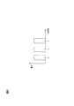
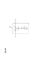
実施例2の整合回路200を図8に示す。整合回路200は、図9に示すような中心周波数をf1、f2、・・・、fNとする第1から第Nの周波数帯域の信号に対する整合回路であり、周波数特性のあるインピーダンスZI(f)を有する増幅素子60と、予め定められたインピーダンスZ0を有する回路(以下、「系の回路50」という。)との間の信号経路に挿入することにより、増幅素子60のインピーダンスZI(f)を系の回路50のインピーダンスZ0に整合する。
FIG. 8 shows a
整合回路200は、第1整合部110と第m(m=2、3、・・・、N)整合部220とから構成される。第m整合部220はそれぞれ直列整合手段221と並列整合手段222とから構成される(なお、m=2については説明の便宜上、実施例1と同様に第2整合部120、直列整合手段121、並列整合手段122とも呼ぶ)。
The
整合回路200において、第1整合部110と第2整合部120の機能は実施例1の整合回路100と全く同じである。そのため、b1及びb2において、増幅素子60のb1及びb2におけるインピーダンスZI(f1)及びZI(f2)は、第1整合部110と第2整合部120により変換され、図8のA点からP2側を見たインピーダンスは共にZ0である。
In the
第m整合部220は、第mの周波数帯bm(中心周波数fm)において、図8のB点からP2側を見たZ0でないインピーダンスZ(fm)を、C点からP2側を見てZ0になるように変換する。
In the m-th frequency band b m (center frequency f m ), the m-
第m整合部220の直列整合手段221の一端は、第m−1整合部220´の直列整合手段221´の一端に接続され、他端は第m+1整合部の直列整合手段の一端に接続される。ただし、m=N(第N整合部220”)の場合は、他端は系の回路50に接続される。第m整合部220の直列整合手段221は、特性インピーダンスがZ0の伝送線路や少なくとも第1から第m−1の周波数帯において上記伝送線路に等価な回路による遅延回路により構成する。このように構成することで、第1から第m−1整合部220´までの各整合部で変換された第1から第m−1の周波数帯における整合状態は第m整合部220の直列整合手段221の存在にかかわらず維持される。従って、第m整合部の直列整合手段221は、bmにおけるインピーダンスの整合をとるために、適宜設定することが可能となる。ここで、少なくともb1からbm-1のすべての周波数帯域において上記伝送線路に等価な回路は、図20A、図20B、図20C、図21A、図21B、図21C、図22A、図22B、図22Cなどを用いることで達成できる。
One end of the
直列整合手段221は、系の回路50と増幅素子60とを結ぶ信号経路上に直列に設けられる。一方、並列整合手段222はその信号経路から枝分かれする形で、系の回路50や増幅素子60と並列に設けられる。
The serial matching means 221 is provided in series on a signal path connecting the
並列整合手段222は、一端が直列整合手段221の他端で信号経路に接続され、他端は接地される。並列整合手段222はbmのインピーダンス整合を行うため、適宜リアクタンス値を設定し、インピーダンスを調整する機能を担う。しかし、b1からbm-1と同時にbmでの整合をとるためには、並列整合手段222は、第1から第m−1整合部で変換されたb1からbm-1におけるインピーダンスZ0に影響を与えるものであってはならない。このような機能、要件を満たすべく、並列整合手段222は2つのブロックの直列接続により構成する。第1並列ブロック222aは、b1からbm-1のすべての周波数帯の信号に対し並列整合手段222を信号経路から切り離すためのスイッチの役割をなすブロックである。また、第2並列ブロック222bは、bmにおけるインピーダンス変換に際し、適切なリアクタンス値を設定するためのブロックである。
One end of the parallel matching means 222 is connected to the signal path at the other end of the series matching means 221, and the other end is grounded. The
第1並列ブロック222aは、b1からbm-1のすべての周波数帯において信号経路との接続点がインピーダンス開放状態(=接続点から並列整合手段222側を見たインピーダンスが無限大又はb1からbm-1のすべての周波数帯での整合に影響を与えない程度に大)となるように設計する。このようにインピーダンス開放状態を作ることにより、スイッチ素子を用いてON/OFFすることなく、等価的に周波数に応じて、並列整合手段を付加したり切り離したりすることができる。b1からbm-1のすべての周波数帯におけるインピーダンス開放状態の作り方としては、例えば第1並列ブロック222aを、キャパシタとインダクタの並列共振回路として構成する場合には、共振周波数がfm−1以上でf1以下になるように構成することが考えられる。特に、両周波数が離れている場合には各中心周波数を平均した周波数を共振周波数とするキャパシタとインダクタの並列共振回路として構成することが考えられる。更に、図10で示すような共振周波数が各周波数帯域に対応するキャパシタとインダクタの並列共振回路222a1、222a2、・・・、222a(m−1)を直列接続する構成によっても、各周波数帯域においてインピーダンス開放状態を実現することができる。また、少なくとも並列共振回路222a1、222a2、・・・、222a(m−1)のうちの一つに可変デバイスを用いれば、並列共振回路の数を減らすことができる。
In the first
なお、第1並列ブロック222aと第2並列ブロック222bの並びは逆でも構わない。ただしその場合、インピーダンス開放部分が両ブロックの接続点に発生するため、信号経路に接続された第2並列ブロック222bが、b1からbm-1におけるインピーダンスの整合状態に影響を与えてしまうおそれがある。そこで、この場合には第2並列ブロック222bを集中定数素子により構成することで影響を低減できる。これにより、信号経路との接続点をインピーダンス開放状態とし並列整合手段222が信号経路から切り離されていると考えることができる。また、このように第1並列ブロック122aが接地側にある場合はインピーダンス開放状態を例えば、第1並列ブロック122aを、f1における波長の4分の1の長さの伝送線路で、第1並列ブロック222aをf1における波長の4分の1以上で、fm−1における波長の4分の1以下の長さの伝送線路で、それぞれ構成することにより開放状態を作っても構わない。この時、両周波数が離れている場合には、各中心周波数を平均した周波数における波長の4分の1の長さとすることが考えられる。
Note that the arrangement of the first
第m整合部はこのような構成の下、直列整合手段221と並列整合手段222を適宜設定することで、B点におけるZ(fm)がいかなる値であっても、C点においてZ0になるよう変換することができる。
Under such a configuration, the m-th matching unit appropriately sets the
以上のような第m整合部におけるbmのインピーダンスの整合をm=Nまで同様に行うことで、P1からP2側を見た各周波数帯のインピーダンスをすべてZ0に整合することができる。 The matching of the impedance of b m by performing in the same manner until m = N, can be matched to all of the impedance of each frequency band viewed P2 side from P1 Z 0 in the m matching portion described above.
そして、bmの信号の整合のみに係る並列整合手段222の切り離し・接続を物理的スイッチを用いることなく、入力された信号の周波数帯に応じて自動的に行うことができるため、第1から第NのN個の周波数帯の信号が同時に入力された場合でも同時に整合をとることができ、なおかつ、スイッチのON抵抗損失のない低損失なマルチバンド整合回路を実現することができる。 Since the parallel matching means 222 relating only to the matching of the b m signal can be disconnected and connected automatically according to the frequency band of the input signal without using a physical switch, Even when signals in the Nth N frequency bands are input at the same time, matching can be achieved at the same time, and a low-loss multiband matching circuit without switch ON resistance loss can be realized.
なお、整合回路200の構成や整合の原理に係るその他の事項は、整合回路100と同様であるため、ここでの説明は省略する。
Note that the other items related to the configuration of the
実施例3のマルチバンド整合回路400の構成例を図26に示す。マルチバンド整合回路400は、第1整合部410と第2整合部420とからなり、第2整合部420は、直列整合手段421と並列整合手段422とからなる。また、並列整合手段422は第1並列ブロック422aと第2並列ブロック422bとからなる。つまり、構成の骨格はマルチバンド整合回路100と同様である。しかし、マルチバンド整合回路400においては、第1整合部410はb1からbmに対応できるマルチバンド整合回路である。また、第2整合部420における直列整合手段421として例えば図21Bの可変回路を適用し、第1並列ブロック422aに可変デバイス(例えばインダクタと可変キャパシタとの並列共振回路)を適用し、第2並列ブロック422bに可変デバイス(例えば可変キャパシタ)を適用する。このような構成をとることで、bm+1からbNのバンドに対し新たに整合可能となり、また、第1並列ブロック422aの可変デバイスを調整することにより、共振周波数をf1からfmの間で変化させることができる。そのため、b1からbmのうちの1つと、bm+1からbNのうちの1つとの任意の組み合わせの2つの周波数帯域に対して同時に整合可能となる。なお、直列整合手段421には図20A、図20B、図20C、図21A、図21B、図21C、図22A、図22Bのような可変回路を用いることができる。第2並列ブロック422bには可変キャパシタの他、可変インダクタやそれと等価な図22A、図22Bなどの回路も適用できる。
A configuration example of the
実施例1〜3で説明した各整合回路を用いることで、マルチバンド増幅器を構成することができる。図11は増幅素子60とその両側に入力整合回路500aと出力整合回路500bとを配したマルチバンド増幅器500の構成例である。なお、図11は各整合回路500a、500bとして整合回路100を用いて2周波数帯対応のマルチバンド増幅器を構成した例であるが、各整合回路500a、500bとして整合回路200を用いることでN周波数帯対応のマルチバンド増幅器を構成することができる。
By using each matching circuit described in the first to third embodiments, a multiband amplifier can be configured. FIG. 11 shows a configuration example of a
なお、増幅素子60の種類については特に限定は無く、例えばFET(Field Effect Transistor)、HBT(Heterojunction Bipolar Transistor)等が挙げられる。
The type of the amplifying
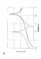
〔効果の確認〕
図11に示すマルチバンド増幅器500において、増幅素子にFETを用い、各整合回路500a、bをf1を2.6GHz、f2を1.9GHzとして構成した場合の周波数−利得特性を図12の実線に、入力ポートP1及び出力ポートP2における周波数−反射減衰特性を図12の点線に示す。
[Confirmation of effect]
In the
第1整合部110は伝送線路を用いて構成され、b1で増幅素子20のインピーダンスZI(f1)をインピーダンスZ0に整合する。また、b1での整合に影響しないよう、第1直列整合手段121として、b1において整合インピーダンスと同じ50Ωとなる伝送線路を用いた。第1並列ブロックにはキャパシタを用い、第2並列ブロックには共振周波数がf1(2.6GHz)になるようインダクタとキャパシタとによる並列共振回路として構成した。
The
図12の点線からわかるように、設計周波数である2.6GHzと1.9GHzにおいて反射が少なく、整合が取れていることがわかる。また、図12の実線からわかるように、利得についても各整合周波数において十分に得られていることがわかる。 As can be seen from the dotted line in FIG. 12, it can be seen that there is little reflection at the design frequencies of 2.6 GHz and 1.9 GHz and matching is achieved. Further, as can be seen from the solid line in FIG. 12, it is understood that the gain is sufficiently obtained at each matching frequency.
10、20 増幅器 30 スイッチ 41、42 整合回路
50 系の回路 60 増幅素子
100、200、300、400、500a、500b マルチバンド整合回路
110、410 第1整合部 120、420 第2整合部
121、221、421 直列整合手段 122、222、422 並列整合手段
122a、222a、422a 第1並列ブロック
122b、222b、422b 第2並列ブロック
151 主整合ブロック 152 遅延回路 153 スイッチ
154 副整合ブロック
220 第m整合部
500 マルチバンド電力増幅器
10, 20
Claims (15)
一端が上記回路素子に接続され、第1の周波数帯域における上記回路素子のインピーダンスをZ0に変換する第1整合部と、
一端が上記第1整合部の他端に接続され、他端が上記系の回路に接続され、特性インピーダンスが系の回路のインピーダンスZ0に等しい伝送線路や少なくとも第1の周波数帯域で上記伝送線路に等価な回路である直列整合手段と、一端が上記直列整合手段の他端で上記信号経路に接続され、他端が接地される並列整合手段と、からなる第2整合部と、
を備え、
上記並列整合手段は、上記第1の周波数帯域において上記信号経路との接続点がインピーダンス開放状態となるように構成され、
上記直列整合手段及び上記並列整合手段を適宜設計することにより第2の周波数帯域における上記回路素子のインピーダンスをZ0に整合する
マルチバンド整合回路。 Two frequencies inserted into a signal path between a circuit element having an impedance Z I (f) having frequency characteristics and a circuit having a predetermined impedance Z 0 (hereinafter referred to as “system circuit”). A multi-band matching circuit for matching the impedance Z I (f) of the circuit element with the impedance Z 0 of the system circuit in the band,
One end is connected to the circuit element, a first matching unit for converting the impedance of the circuit element in a first frequency band to Z 0,
One end connected to the other end of the first matching unit and the other end is connected to the system circuit, a transmission line characteristic impedance is equal to the impedance Z 0 of the circuit of the system and at least a first frequency band in the transmission line A second matching unit comprising: a serial matching unit, which is an equivalent circuit, and a parallel matching unit having one end connected to the signal path at the other end of the series matching unit and the other end grounded;
With
The parallel matching means is configured such that a connection point with the signal path is in an impedance open state in the first frequency band,
A multiband matching circuit for matching the impedance of the circuit element in the second frequency band to Z 0 by appropriately designing the series matching means and the parallel matching means.
上記並列整合手段は、一端が上記信号経路に接続される第1並列ブロックと、一端が当該第1並列ブロックの他端と接続され、他端が接地される第2並列ブロックとからなり、
上記第1並列ブロックは、上記第1の周波数帯域において、上記信号経路との接続点がインピーダンス開放状態となるように構成される
マルチバンド整合回路。 The multiband matching circuit according to claim 1,
The parallel matching means includes a first parallel block having one end connected to the signal path, and a second parallel block having one end connected to the other end of the first parallel block and the other end grounded.
The first parallel block is a multiband matching circuit configured such that a connection point with the signal path is in an open impedance state in the first frequency band.
上記並列整合手段は、一端が上記信号経路に接続される第2並列ブロックと、一端が当該第2並列ブロックの他端と接続され、他端が接地される第1並列ブロックとからなり、
上記第2並列ブロックは、集中定数素子により構成され、
上記第1並列ブロックは、上記第1の周波数帯域において、上記第2並列ブロックとの接続点がインピーダンス開放状態となるように構成される
マルチバンド整合回路。 The multiband matching circuit according to claim 1,
The parallel matching means includes a second parallel block having one end connected to the signal path, and a first parallel block having one end connected to the other end of the second parallel block and the other end grounded.
The second parallel block includes a lumped constant element,
The first parallel block is a multiband matching circuit configured such that a connection point between the first parallel block and the second parallel block is in an open impedance state in the first frequency band.
上記第1並列ブロックは、共振周波数が上記第1の周波数帯域の中心周波数f1に等しい、キャパシタとインダクタの並列回路であるマルチバンド整合回路。 In the multiband matching circuit according to claim 2 or 3,
The first parallel block is a multiband matching circuit which is a parallel circuit of a capacitor and an inductor, the resonance frequency of which is equal to the center frequency f1 of the first frequency band.
上記第1並列ブロックは、上記第1の周波数帯域の中心周波数f1における波長の4分の1の長さの伝送線路であるマルチバンド整合回路。 The multi-band matching circuit according to claim 3,
The first parallel block is a multiband matching circuit which is a transmission line having a length of a quarter of the wavelength at the center frequency f1 of the first frequency band.
一端が上記回路素子に接続され、第1の周波数帯域における上記回路素子のインピーダンスをZ0に変換する第1整合部と、
一端が第m−1整合部(m=2、3、・・・、N)の他端に接続され、特性インピーダンスが系の回路のインピーダンスZ0に等しい伝送線路や少なくとも第1から第m−1の各周波数帯域において上記伝送線路に等価な回路である直列整合手段と、一端が上記直列整合手段の他端で上記信号経路に接続され、他端が接地される並列整合手段と、からなる第m整合部と、
を備え、
第N整合部の直列整合手段の他端は上記系の回路に接続され、
上記第m整合部の並列整合手段は、第1から第m−1の各周波数帯域において上記信号経路との接続点がインピーダンス開放状態となるように構成され、
上記第m整合部の直列整合手段及び上記第m整合部の並列整合手段を適宜設計することにより第mの周波数帯域における上記回路素子のインピーダンスをZ0に整合する
マルチバンド整合回路。 Inserted into a signal path between a circuit element having an impedance Z I (f) having frequency characteristics and a circuit having a predetermined impedance Z 0 (hereinafter referred to as “system circuit”), Multi-band matching circuit for matching the impedance Z I (f) of the circuit element with the impedance Z 0 of the system circuit in the Nth frequency band (N ≧ 3, center frequency f 1 > f 2 >...> F N ) Because
One end is connected to the circuit element, a first matching unit for converting the impedance of the circuit element in a first frequency band to Z 0,
One end (m-1) -th matching unit (m = 2,3, ···, N ) is connected to the other end of the characteristic impedance transmission line and at least a first equal to the impedance Z 0 of the circuit of the system m- A serial matching unit that is a circuit equivalent to the transmission line in each frequency band, and a parallel matching unit having one end connected to the signal path at the other end of the series matching unit and the other end grounded. The mth matching section;
With
The other end of the series matching means of the Nth matching unit is connected to the above system circuit,
The parallel matching means of the m-th matching unit is configured such that the connection point with the signal path is in an impedance open state in each of the first to m−1 frequency bands.
A multiband matching circuit that matches the impedance of the circuit element in the mth frequency band to Z 0 by appropriately designing the series matching means of the mth matching section and the parallel matching means of the mth matching section.
上記第m整合部の並列整合手段は、一端が上記信号経路に接続される第1並列ブロックと、一端が当該第1並列ブロックの他端と接続され、他端が接地される第2並列ブロックとからなり、
上記第1並列ブロックは、上記第1から第m−1の各周波数帯域において、上記信号経路との接続点がインピーダンス開放状態となるように構成される
マルチバンド整合回路。 The multi-band matching circuit according to claim 6,
The parallel matching means of the m-th matching unit includes a first parallel block having one end connected to the signal path, and a second parallel block having one end connected to the other end of the first parallel block and the other end grounded. And consist of
The first parallel block is a multiband matching circuit configured such that a connection point with the signal path is in an open impedance state in each of the first to m−1 frequency bands.
上記第m整合部の並列整合手段は、一端が上記信号経路に接続される第2並列ブロックと、一端が当該第2並列ブロックの他端と接続され、他端が接地される第1並列ブロックとからなり、
上記第2並列ブロックは、集中定数素子により構成され、
上記第1並列ブロックは、上記第1から第m−1の各周波数帯域において、上記第2並列ブロックとの接続点がインピーダンス開放状態となるように構成される
マルチバンド整合回路。 The multi-band matching circuit according to claim 6,
The parallel matching means of the m-th matching unit includes a second parallel block having one end connected to the signal path, a first parallel block having one end connected to the other end of the second parallel block and the other end grounded. And consist of
The second parallel block includes a lumped constant element,
The first parallel block is a multiband matching circuit configured such that a connection point with the second parallel block is in an open impedance state in each of the first to m−1 frequency bands.
上記第1並列ブロックは、共振周波数が上記第m−1の周波数帯域の中心周波数fm−1以上で、上記第1の周波数帯域の中心周波数f1以下である、キャパシタとインダクタの並列回路であるマルチバンド整合回路。 The multiband matching circuit according to any one of claims 7 and 8,
The first parallel block is a parallel circuit of a capacitor and an inductor whose resonance frequency is not less than the center frequency f m−1 of the m−1 frequency band and not more than the center frequency f 1 of the first frequency band. A multiband matching circuit.
上記第1並列ブロックは、共振周波数がそれぞれ第1から第m−1の周波数帯域の中心周波数f1、f2、・・・、fm−1である、m−1段のキャパシタとインダクタの並列回路の直列接続であるマルチバンド整合回路。 The multiband matching circuit according to any one of claims 7 and 8,
The first parallel block includes m-1 stage capacitors and inductors having resonance frequencies of center frequencies f 1 , f 2 ,..., F m−1 in the first to m−1 frequency bands, respectively. A multiband matching circuit that is a series connection of parallel circuits.
上記第1並列ブロックは伝送線路で構成され、その長さが上記第1の周波数帯域の中心周波数f1における波長の4分の1以上で、上記第m−1の周波数帯域の中心周波数fm−1における波長の4分の1以下であるマルチバンド整合回路。 The multiband matching circuit according to claim 8,
The first parallel block is composed of a transmission line, the length of which is not less than ¼ of the wavelength at the center frequency f 1 of the first frequency band, and the center frequency f m of the m−1th frequency band. A multiband matching circuit having a wavelength equal to or less than a quarter of the wavelength at -1 .
一端が上記回路素子に接続され、第1から第m(m≧2)のいずれかの周波数帯域における上記回路素子のインピーダンスをZ0に変換する第1整合部と、
一端が上記第1整合部の他端に接続され、他端が上記系の回路に接続され、特性インピーダンスが系の回路のインピーダンスZ0に等しい伝送線路や少なくとも上記第1から第mのいずれかの周波数帯域で上記伝送線路に等価な回路である直列整合手段と、一端が上記直列整合手段の他端で上記信号経路に接続され、他端が接地される並列整合手段と、からなる第2整合部と、
を備え、
上記並列整合手段は、上記第1から第mのいずれかの周波数帯域において上記信号経路との接続点がインピーダンス開放状態となるように構成され、
上記直列整合手段及び上記並列整合手段を適宜設計することにより第m+1から第N(N≧3)のいずれかの周波数帯域における上記回路素子のインピーダンスをZ0に整合する
マルチバンド整合回路。 Two frequencies inserted into a signal path between a circuit element having an impedance Z I (f) having frequency characteristics and a circuit having a predetermined impedance Z 0 (hereinafter referred to as “system circuit”). A multi-band matching circuit for matching the impedance Z I (f) of the circuit element with the impedance Z 0 of the system circuit in the band,
A first matching unit having one end connected to the circuit element and converting the impedance of the circuit element in any one of the first to m-th (m ≧ 2) frequency bands to Z 0 ;
One end connected to the other end of the first matching unit and the other end is connected to the system circuit, any of the transmission lines and at least said first equal characteristic impedance to the impedance Z 0 of the circuit of the system of the m And a parallel matching unit having one end connected to the signal path at the other end of the series matching unit and the other end grounded. A matching section;
With
The parallel matching means is configured such that a connection point with the signal path is in an impedance open state in any one of the first to m-th frequency bands,
Multiband matching circuit the impedance of the circuit element in any frequency band from the m + 1 the N (N ≧ 3) aligned with the Z 0 by appropriately designing the series matching section and the parallel matching section.
上記並列整合手段は、一端が上記信号経路に接続される可変デバイスである第1並列ブロックと、一端が当該第1並列ブロックの他端と接続され、他端が接地される可変デバイスである第2並列ブロックとからなり、
上記第1並列ブロックは、上記第1から第mのいずれかの周波数帯域において、上記信号経路との接続点がインピーダンス開放状態となるように構成される
マルチバンド整合回路。 The multi-band matching circuit according to claim 12,
The parallel matching means includes a first parallel block that is a variable device having one end connected to the signal path, and a variable device having one end connected to the other end of the first parallel block and the other end grounded. It consists of two parallel blocks,
The first parallel block is a multiband matching circuit configured such that a connection point with the signal path is in an open impedance state in any one of the first to m-th frequency bands.
上記第1並列ブロックは、可変キャパシタとインダクタの並列共振回路であるマルチバンド整合回路。 The multi-band matching circuit according to claim 13,
The first parallel block is a multiband matching circuit which is a parallel resonant circuit of a variable capacitor and an inductor.
Priority Applications (5)
| Application Number | Priority Date | Filing Date | Title |
|---|---|---|---|
| JP2010006885A JP5453120B2 (en) | 2009-01-30 | 2010-01-15 | Multiband matching circuit and multiband power amplifier |
| KR1020100006932A KR101156450B1 (en) | 2009-01-30 | 2010-01-26 | Multiband matching circuit and multiband power amplifier |
| US12/695,442 US8487713B2 (en) | 2009-01-30 | 2010-01-28 | Multiband matching circuit and multiband power amplifier |
| EP10151927A EP2214310A1 (en) | 2009-01-30 | 2010-01-28 | Multiband matching circuit and multiband power amplifier |
| CN2010101081012A CN101795120B (en) | 2009-01-30 | 2010-02-01 | Multiband matching circuit and multiband power amplifier |
Applications Claiming Priority (3)
| Application Number | Priority Date | Filing Date | Title |
|---|---|---|---|
| JP2009020581 | 2009-01-30 | ||
| JP2009020581 | 2009-01-30 | ||
| JP2010006885A JP5453120B2 (en) | 2009-01-30 | 2010-01-15 | Multiband matching circuit and multiband power amplifier |
Publications (2)
| Publication Number | Publication Date |
|---|---|
| JP2010200310A true JP2010200310A (en) | 2010-09-09 |
| JP5453120B2 JP5453120B2 (en) | 2014-03-26 |
Family
ID=42046391
Family Applications (1)
| Application Number | Title | Priority Date | Filing Date |
|---|---|---|---|
| JP2010006885A Expired - Fee Related JP5453120B2 (en) | 2009-01-30 | 2010-01-15 | Multiband matching circuit and multiband power amplifier |
Country Status (5)
| Country | Link |
|---|---|
| US (1) | US8487713B2 (en) |
| EP (1) | EP2214310A1 (en) |
| JP (1) | JP5453120B2 (en) |
| KR (1) | KR101156450B1 (en) |
| CN (1) | CN101795120B (en) |
Cited By (6)
| Publication number | Priority date | Publication date | Assignee | Title |
|---|---|---|---|---|
| JP2014072593A (en) * | 2012-09-28 | 2014-04-21 | Taiyo Yuden Co Ltd | Impedance matching circuit and antenna system |
| JP2014519229A (en) * | 2011-04-27 | 2014-08-07 | アルカテル−ルーセント | Isolated zero degree reactive radio frequency high power coupler |
| JP2016539563A (en) * | 2013-11-07 | 2016-12-15 | クアルコム,インコーポレイテッド | Low noise amplifier matching |
| JP2017521012A (en) * | 2014-07-14 | 2017-07-27 | コヴィディエン リミテッド パートナーシップ | Dual-band power amplifier circuit for microwave ablation |
| KR20180022666A (en) | 2015-06-09 | 2018-03-06 | 국립대학법인 전기통신대학 | Multiband Amplifier and Dual Band Amplifier |
| JP2019537831A (en) * | 2016-11-08 | 2019-12-26 | サントル ナショナル ドゥ ラ ルシェルシュ シアンティフィック | Circuits for impedance matching between a generator and a load at multiple frequencies, assemblies including such circuits, and related uses |
Families Citing this family (23)
| Publication number | Priority date | Publication date | Assignee | Title |
|---|---|---|---|---|
| DE102010011411B4 (en) * | 2010-03-15 | 2015-07-02 | Qualcomm Technologies, Inc. (N.D.Ges.D. Staates Delaware) | Adjustable capacitive element |
| US8947317B2 (en) * | 2010-07-28 | 2015-02-03 | National University Corporation Kyoto Institute Of Technology | Microwave resonator configured by composite right/left-handed meta-material and antenna apparatus provided with the microwave resonator |
| JP5498314B2 (en) * | 2010-08-09 | 2014-05-21 | 株式会社Nttドコモ | Variable impedance matching circuit |
| US20130178168A1 (en) * | 2012-01-10 | 2013-07-11 | Chunjie Duan | Multi-Band Matching Network for RF Power Amplifiers |
| JP5874441B2 (en) * | 2012-02-29 | 2016-03-02 | 富士通株式会社 | amplifier |
| KR101452063B1 (en) | 2012-12-10 | 2014-10-16 | 삼성전기주식회사 | Front end module |
| DE102013002227B4 (en) * | 2013-02-11 | 2014-11-13 | Sew-Eurodrive Gmbh & Co Kg | Arrangement for signal transmission and installation with this arrangement |
| CN105009450B (en) * | 2013-02-27 | 2018-11-20 | 新加坡国立大学 | With improved RF- to-DC power conversion efficiency for the RECTIFYING ANTENNA in wireless network |
| US8963644B2 (en) | 2013-03-25 | 2015-02-24 | Mitsubishi Electric Research Laboratories, Inc. | Reconfigurable output matching network for multiple power mode power amplifiers |
| CN103997305A (en) * | 2014-05-19 | 2014-08-20 | 天津大学 | Three-frequency-band radio frequency power amplifier impedance matching circuit |
| US10340876B2 (en) * | 2015-04-17 | 2019-07-02 | Psemi Corporation | Tunable and integrated impedance matching and filter circuit |
| EP3121968A1 (en) * | 2015-07-24 | 2017-01-25 | IMEC vzw | Telecommunications device comprising an ebd circuit, a tunable impedance network and a method for tuning a tunable impedance network |
| CN105161866B (en) * | 2015-08-31 | 2018-09-04 | 宇龙计算机通信科技(深圳)有限公司 | Antenna tuner, multiband aerial and mobile terminal |
| EP4138516A1 (en) * | 2015-12-22 | 2023-02-22 | Thermatool Corp. | High frequency power supply system with closely regulated output for heating a workpiece |
| US10673513B2 (en) * | 2016-03-11 | 2020-06-02 | Akoustis, Inc. | Front end module for 5.2 GHz Wi-Fi acoustic wave resonator RF filter circuit |
| WO2018012275A1 (en) * | 2016-07-15 | 2018-01-18 | 株式会社村田製作所 | Multiplexer, high-frequency front end circuit, and communication terminal |
| CN107591624B (en) * | 2017-08-17 | 2020-08-11 | 海信视像科技股份有限公司 | Antenna and television terminal |
| US10855235B2 (en) * | 2017-12-27 | 2020-12-01 | Murata Manufacturing Co., Ltd. | Power amplifier circuit |
| CN110536534B (en) * | 2019-09-06 | 2024-03-26 | 深圳市恒运昌真空技术股份有限公司 | Impedance adjusting method and device of matching box and radio frequency power supply system |
| CN110781635A (en) * | 2019-09-27 | 2020-02-11 | 上海航天控制技术研究所 | Rapid automatic design method and system for complex system contact list |
| JP2021106334A (en) * | 2019-12-26 | 2021-07-26 | 株式会社村田製作所 | High-frequency circuit |
| CN113242029A (en) * | 2021-05-12 | 2021-08-10 | 西北工业大学深圳研究院 | Multi-frequency impedance matching method based on lumped element |
| CN114785297A (en) * | 2022-04-18 | 2022-07-22 | 深圳飞骧科技股份有限公司 | Power amplifier and input matching network thereof |
Citations (2)
| Publication number | Priority date | Publication date | Assignee | Title |
|---|---|---|---|---|
| JPS5429949A (en) * | 1977-08-10 | 1979-03-06 | Denki Kogyo Co Ltd | Multiple wave matching system |
| JP2008160192A (en) * | 2006-12-20 | 2008-07-10 | Ntt Docomo Inc | Matching circuit and dual band power amplifier |
Family Cites Families (13)
| Publication number | Priority date | Publication date | Assignee | Title |
|---|---|---|---|---|
| JPH1056305A (en) * | 1996-08-09 | 1998-02-24 | Mitsubishi Electric Corp | Impedance matching circuit and thin film probe for measurement |
| JPH10242776A (en) | 1996-12-24 | 1998-09-11 | Murata Mfg Co Ltd | High frequency amplifier |
| CN1367952A (en) | 1999-07-07 | 2002-09-04 | 艾利森公司 | Dual-band. dual-mode power amplifier |
| JP2001111362A (en) * | 1999-10-06 | 2001-04-20 | Nec Corp | Higher harmonic processing circuit and high power efficiency amplifier circuit using the same |
| WO2001045204A1 (en) | 1999-12-15 | 2001-06-21 | Mitsubishi Denki Kabushiki Kaisha | Impedance matching circuit and antenna using impedance matching circuit |
| JP2003174335A (en) * | 2001-12-05 | 2003-06-20 | Mitsubishi Electric Corp | Amplifier |
| US8098114B2 (en) | 2003-03-14 | 2012-01-17 | Ntt Docomo, Inc. | Matching circuit |
| CN1320772C (en) * | 2003-06-05 | 2007-06-06 | 联发科技股份有限公司 | Multi-frequency band low-noise amplifier |
| JP4838536B2 (en) * | 2005-05-20 | 2011-12-14 | 株式会社エヌ・ティ・ティ・ドコモ | Matching circuit |
| JP4178477B2 (en) | 2005-11-24 | 2008-11-12 | 船井電機株式会社 | Data transmission device |
| JP4843455B2 (en) | 2006-10-30 | 2011-12-21 | 株式会社エヌ・ティ・ティ・ドコモ | Matching circuit, multiband amplifier |
| JP5079387B2 (en) | 2007-05-10 | 2012-11-21 | 株式会社エヌ・ティ・ティ・ドコモ | Matching circuit |
| JP2009020581A (en) | 2007-07-10 | 2009-01-29 | Hitachi Information Systems Ltd | Inter-application communication system |
-
2010
- 2010-01-15 JP JP2010006885A patent/JP5453120B2/en not_active Expired - Fee Related
- 2010-01-26 KR KR1020100006932A patent/KR101156450B1/en not_active IP Right Cessation
- 2010-01-28 EP EP10151927A patent/EP2214310A1/en not_active Withdrawn
- 2010-01-28 US US12/695,442 patent/US8487713B2/en not_active Expired - Fee Related
- 2010-02-01 CN CN2010101081012A patent/CN101795120B/en not_active Expired - Fee Related
Patent Citations (2)
| Publication number | Priority date | Publication date | Assignee | Title |
|---|---|---|---|---|
| JPS5429949A (en) * | 1977-08-10 | 1979-03-06 | Denki Kogyo Co Ltd | Multiple wave matching system |
| JP2008160192A (en) * | 2006-12-20 | 2008-07-10 | Ntt Docomo Inc | Matching circuit and dual band power amplifier |
Cited By (8)
| Publication number | Priority date | Publication date | Assignee | Title |
|---|---|---|---|---|
| JP2014519229A (en) * | 2011-04-27 | 2014-08-07 | アルカテル−ルーセント | Isolated zero degree reactive radio frequency high power coupler |
| JP2014072593A (en) * | 2012-09-28 | 2014-04-21 | Taiyo Yuden Co Ltd | Impedance matching circuit and antenna system |
| US9680441B2 (en) | 2012-09-28 | 2017-06-13 | Taiyo Yuden Co., Ltd. | Impedance matching circuit and antenna system |
| JP2016539563A (en) * | 2013-11-07 | 2016-12-15 | クアルコム,インコーポレイテッド | Low noise amplifier matching |
| JP2017521012A (en) * | 2014-07-14 | 2017-07-27 | コヴィディエン リミテッド パートナーシップ | Dual-band power amplifier circuit for microwave ablation |
| KR20180022666A (en) | 2015-06-09 | 2018-03-06 | 국립대학법인 전기통신대학 | Multiband Amplifier and Dual Band Amplifier |
| JP2019537831A (en) * | 2016-11-08 | 2019-12-26 | サントル ナショナル ドゥ ラ ルシェルシュ シアンティフィック | Circuits for impedance matching between a generator and a load at multiple frequencies, assemblies including such circuits, and related uses |
| JP7097376B2 (en) | 2016-11-08 | 2022-07-07 | サントル ナショナル ドゥ ラ ルシェルシュ シアンティフィック | Circuits for impedance matching between generators and loads at multiple frequencies, assemblies containing such circuits, and related uses. |
Also Published As
| Publication number | Publication date |
|---|---|
| JP5453120B2 (en) | 2014-03-26 |
| US8487713B2 (en) | 2013-07-16 |
| CN101795120B (en) | 2013-12-11 |
| EP2214310A1 (en) | 2010-08-04 |
| US20100194487A1 (en) | 2010-08-05 |
| KR20100088534A (en) | 2010-08-09 |
| CN101795120A (en) | 2010-08-04 |
| KR101156450B1 (en) | 2012-06-13 |
Similar Documents
| Publication | Publication Date | Title |
|---|---|---|
| JP5453120B2 (en) | Multiband matching circuit and multiband power amplifier | |
| JP6890146B2 (en) | Front-end architecture, how to handle 2G signals, front-end modules, and radios | |
| US7750756B2 (en) | Matching circuit | |
| JP5102825B2 (en) | Multiband matching circuit and multiband power amplifier | |
| EP1916772B1 (en) | Matching circuit and multi-band amplifier | |
| JP4464919B2 (en) | Matching circuit | |
| US7710217B2 (en) | Matching circuit and dual-band power amplifier | |
| US7656249B2 (en) | Matching circuit | |
| JP4838572B2 (en) | Stabilization circuit, multiband amplifier circuit | |
| KR101594192B1 (en) | Impedance matching circuit capable of efficiently isolating paths for multi-band power amplifier | |
| JP2012044436A (en) | Multiband matching circuit | |
| JP2011015242A (en) | Radio frequency power amplifier | |
| JP2018085635A (en) | Power amplifier | |
| WO2005048448A1 (en) | High frequency amplifier | |
| JP2007329669A (en) | Power amplifying apparatus | |
| KR101589587B1 (en) | T-type dual band impedance matching circuit and the design method thereof | |
| JP2004364068A (en) | Frequency band variable amplifier | |
| JP2013138513A (en) | Multiband matching circuit |
Legal Events
| Date | Code | Title | Description |
|---|---|---|---|
| A621 | Written request for application examination |
Free format text: JAPANESE INTERMEDIATE CODE: A621 Effective date: 20110822 |
|
| A131 | Notification of reasons for refusal |
Free format text: JAPANESE INTERMEDIATE CODE: A131 Effective date: 20120918 |
|
| A521 | Written amendment |
Free format text: JAPANESE INTERMEDIATE CODE: A523 Effective date: 20121114 |
|
| A02 | Decision of refusal |
Free format text: JAPANESE INTERMEDIATE CODE: A02 Effective date: 20130702 |
|
| A521 | Written amendment |
Free format text: JAPANESE INTERMEDIATE CODE: A523 Effective date: 20130830 |
|
| A911 | Transfer to examiner for re-examination before appeal (zenchi) |
Free format text: JAPANESE INTERMEDIATE CODE: A911 Effective date: 20130909 |
|
| TRDD | Decision of grant or rejection written | ||
| A01 | Written decision to grant a patent or to grant a registration (utility model) |
Free format text: JAPANESE INTERMEDIATE CODE: A01 Effective date: 20131224 |
|
| A61 | First payment of annual fees (during grant procedure) |
Free format text: JAPANESE INTERMEDIATE CODE: A61 Effective date: 20140106 |
|
| R150 | Certificate of patent or registration of utility model |
Ref document number: 5453120 Country of ref document: JP Free format text: JAPANESE INTERMEDIATE CODE: R150 Free format text: JAPANESE INTERMEDIATE CODE: R150 |
|
| R250 | Receipt of annual fees |
Free format text: JAPANESE INTERMEDIATE CODE: R250 |
|
| R250 | Receipt of annual fees |
Free format text: JAPANESE INTERMEDIATE CODE: R250 |
|
| R250 | Receipt of annual fees |
Free format text: JAPANESE INTERMEDIATE CODE: R250 |
|
| LAPS | Cancellation because of no payment of annual fees |