JP2010200220A - Timing adjustment circuit, and method of adjusting the same - Google Patents
Timing adjustment circuit, and method of adjusting the same Download PDFInfo
- Publication number
- JP2010200220A JP2010200220A JP2009045332A JP2009045332A JP2010200220A JP 2010200220 A JP2010200220 A JP 2010200220A JP 2009045332 A JP2009045332 A JP 2009045332A JP 2009045332 A JP2009045332 A JP 2009045332A JP 2010200220 A JP2010200220 A JP 2010200220A
- Authority
- JP
- Japan
- Prior art keywords
- timing
- reception timing
- digital signal
- reception
- adjustment circuit
- Prior art date
- Legal status (The legal status is an assumption and is not a legal conclusion. Google has not performed a legal analysis and makes no representation as to the accuracy of the status listed.)
- Pending
Links
Images


Landscapes
- Near-Field Transmission Systems (AREA)
- Synchronisation In Digital Transmission Systems (AREA)
Abstract
【課題】従来のタイミング調整回路では、データ受信用クロックのタイミング調整に時間を要し、精度の高いデータ処理ができないという問題があった。
【解決手段】本発明にかかるタイミング調整回路は、無線タグから送信される送信信号の受信タイミングを調整するタイミング調整回路であって、送信信号のプリアンブルを構成するアナログ信号を、基準クロックに基づいてデジタル信号に変換するADC200と、ADC200により変換された第1のデジタル信号と、第1のデジタル信号と時間的に隣接して変換された第2のデジタル信号と、からゼロクロスを検出するゼロクロス検出回路201と、基準クロックとゼロクロスの検出回数とに基づいて受信タイミングを決定する受信タイミング決定回路202と、を備える。このような構成により、データ受信用クロックのタイミング調整に要する時間を短縮し、精度の高いデータ処理を可能にすることができる。
【選択図】図2A conventional timing adjustment circuit has a problem in that it takes time to adjust the timing of a data reception clock, and data processing with high accuracy cannot be performed.
A timing adjustment circuit according to the present invention is a timing adjustment circuit for adjusting a reception timing of a transmission signal transmitted from a radio tag, and an analog signal constituting a preamble of the transmission signal is converted based on a reference clock. Zero cross detection circuit for detecting zero cross from ADC 200 that converts to digital signal, first digital signal that is converted by ADC 200, and second digital signal that is converted temporally adjacent to the first digital signal 201 and a reception timing determination circuit 202 that determines the reception timing based on the reference clock and the number of zero cross detections. With such a configuration, it is possible to reduce the time required for adjusting the timing of the data reception clock and to perform highly accurate data processing.
[Selection] Figure 2
Description
本発明は、タイミング調整回路及びその調整方法に関する。 The present invention relates to a timing adjustment circuit and an adjustment method thereof.
無線タグと無線タグリーダライタと間の無線通信技術として知られているRFID(Radio Frequency Identification)技術は、物流や電子マネーなどの分野に広く用いられ、様々なプロトコル(通信規格)が規格化されている。RFIDシステムは、概してRFIDタグとRFIDリーダライタを備えている。 RFID (Radio Frequency Identification) technology, which is known as a wireless communication technology between a wireless tag and a wireless tag reader / writer, is widely used in fields such as logistics and electronic money, and various protocols (communication standards) have been standardized. Yes. An RFID system generally includes an RFID tag and an RFID reader / writer.
ISO18092で定められたプロトコルの場合の例を示す。図5に示すように、データフレームは、主として、「Preamble+SYNC+LENGTH」から構成されるプリアンブルと、データコマンドを含むペイロードと、データコマンドが正しく読みこまれたかどうかを検出(誤り検出)するために用いられるCRCデータとによって構成される。 An example in the case of a protocol defined by ISO18092 will be shown. As shown in FIG. 5, the data frame is mainly used to detect (error detection) whether a preamble including “Preamble + SYNC + LENGTH”, a payload including a data command, and whether the data command is read correctly. CRC data.
ここで、RFIDタグからの応答信号には遅延やジッタ等の揺らぎが発生する。そのため、RFIDリーダライタがこの応答信号を正しく受信できないという問題がある。そこで、RFIDタグからの応答信号を正しく受信できるようにRFIDリーダライタの受信クロックの位相、周期等が制御される。具体的には、RFIDタグからの応答信号に含まれるプリアンブルに基づいて受信用クロックの位相等が制御される。そして、この受信用クロックに同期してプリアンブルに続くデータフレームの読み込みが行われる。 Here, fluctuations such as delay and jitter occur in the response signal from the RFID tag. Therefore, there is a problem that the RFID reader / writer cannot receive the response signal correctly. Therefore, the phase, period, etc. of the reception clock of the RFID reader / writer are controlled so that the response signal from the RFID tag can be correctly received. Specifically, the phase or the like of the reception clock is controlled based on the preamble included in the response signal from the RFID tag. Then, the data frame following the preamble is read in synchronization with the reception clock.
データ受信装置においてデータ受信用クロックをタイミング調整する方法が特許文献1に開示されている。図7に、特許文献1に記載されている同期引き込み装置500のブロック図を示す。図7に示す同期引き込み装置500は、ユニワード(UW)検出器502、TDMAタイミング生成器507、位相比較器506、マイクロプロセッサ520、補正カウンタ524、1/n分周器503、補正器504、1/m分周器505を有する。
A method of adjusting the timing of a data reception clock in a data reception apparatus is disclosed in
ユニワード検出器502は、基地局からの電波を復調器501で復調して得られるシリアルのデジタル受信データ及び受信クロックからユニークワードを検出しその検出タイミングを出力する。TDMAタイミング生成器507は、シンボルクロックでTDMAタイミングを生成し、自局の送信スロットタイミング及び受信スロットタイミングを生成する。位相検出器506は、ユニークワードの検出タイミングに応じて受信時のシンボルタイミングと自局のシンボルクロックの位相とを比較し、その位相差の値を出力する。マイクロプロセッサ520は、位相検出器506が出力する位相差の値に基づき基本クロックの補正量を算出するとともに進み/遅れ補正の指示を行う。補正カウンタ524は、マイクロプロセッサ520から指示された補正量から補正タイミングを生成する。1/n分周器503は、受信時のシンボルタイミング周期のn×m倍のクロックを1/n分周し前記基本クロックを生成する。補正器504は、補正カウンタ524が出力する補正タイミングが進み補正の場合は基本クロックに対してクロックの削除、遅れ補正の場合は基本クロックに対してクロックの挿入を行い、補正操作を行った同期補正クロックを出力する。1/m分周器505は、その同期補正されたクロックを1/m分周し、自局のシンボルタイミングを示すシンボルクロックを出力する。
A
同期引き込み装置500では、位相検出器506で検出された受信時のシンボルタイミングと自局のシンボルクロックの位相との位相差の値に基づきマイクロプロセッサ520が基本クロックの補正量を算出する。そして、算出された補正量で補正された基本クロックに基づき動作することで、基地局との動作の整合性を確保する。
In the synchronization pull-in
しかし、図7に示す回路の場合、マイクロプロセッサ520において補正量を算出しているため、その演算処理に時間を要するという問題があった。近年、データ通信速度が向上しているため、補正タイミングの遅れによりデータ処理を正しく処理できない可能性がある。
However, in the case of the circuit shown in FIG. 7, since the correction amount is calculated by the
上述のように、従来のデータ受信装置等に備えられたタイミング調整回路では、データ受信用クロックのタイミング調整のための演算処理に時間を要し、データ受信装置等がデータを正しく処理できないという問題があった。 As described above, in the timing adjustment circuit provided in the conventional data reception device or the like, the calculation processing for adjusting the timing of the data reception clock takes time, and the data reception device or the like cannot correctly process the data. was there.
本発明にかかるタイミング調整回路は、無線タグから送信される送信信号の受信タイミングを調整するタイミング調整回路であって、前記送信信号のプリアンブルを構成するアナログ信号を、基準クロックに基づいてデジタル信号に変換するA/Dコンバータと、前記A/Dコンバータにより変換された第1のデジタル信号と、当該第1のデジタル信号と時間的に隣接して変換された第2のデジタル信号と、からゼロクロスを検出するゼロクロス検出回路と、前記基準クロックと前記ゼロクロスの検出回数とに基づいて前記受信タイミングを決定する受信タイミング決定回路と、を備える。 A timing adjustment circuit according to the present invention is a timing adjustment circuit that adjusts the reception timing of a transmission signal transmitted from a wireless tag, and converts an analog signal constituting a preamble of the transmission signal into a digital signal based on a reference clock. A zero cross is obtained from the A / D converter to be converted, the first digital signal converted by the A / D converter, and the second digital signal converted in time adjacent to the first digital signal. A zero-cross detection circuit for detecting, and a reception timing determination circuit for determining the reception timing based on the reference clock and the number of times of detection of the zero-cross.
また、本発明にかかるタイミング調整回路の調整方法は、無線タグから送信される送信信号の受信タイミングを調整するタイミング調整回路であって、前記送信信号のプリアンブルを構成するアナログ信号を、基準クロックに基づいてデジタル信号に変換し、変換された第1のデジタル信号と、当該第1のデジタル信号と時間的に隣接して変換された第2のデジタル信号と、からゼロクロスを検出し、前記基準クロックと前記ゼロクロスの検出回数とに基づいて前記受信タイミングを決定する。 The timing adjustment circuit adjustment method according to the present invention is a timing adjustment circuit for adjusting the reception timing of a transmission signal transmitted from a wireless tag, wherein an analog signal constituting a preamble of the transmission signal is used as a reference clock. And converting the digital signal into a digital signal, detecting a zero cross from the converted first digital signal and the second digital signal converted in time adjacent to the first digital signal, and detecting the reference clock And the reception timing is determined based on the number of times of detection of the zero cross.
上述のような構成のタイミング調整回路及びその調整方法により、データ受信用クロックのタイミング調整に要する時間を短縮し、精度の高いデータ処理を可能にすることができる。 With the timing adjustment circuit and the adjustment method configured as described above, it is possible to reduce the time required for adjusting the timing of the data reception clock and to perform highly accurate data processing.
本発明により、データ受信用クロックのタイミング調整に要する時間を短縮し、精度の高いデータ処理を可能にするタイミング調整回路を提供することができる。 According to the present invention, it is possible to provide a timing adjustment circuit that shortens the time required for adjusting the timing of the data reception clock and enables highly accurate data processing.
以下では、本発明を適用した具体的な実施の形態について、図面を参照しながら詳細に説明する。各図面において、同一要素には同一の符号が付されており、説明の明確化のため、必要に応じて重複説明は省略される。 Hereinafter, specific embodiments to which the present invention is applied will be described in detail with reference to the drawings. In the drawings, the same elements are denoted by the same reference numerals, and redundant description is omitted as necessary for the sake of clarity.
なお、本発明の実施の形態では、無線タグリーダライタをRFIDリーダライタとし、無線タグをRFIDタグとして説明する。なお、例えば、プリアンブルのような固定パタンに基づいてその後のデータ処理を決定する通信方式を用いるものであればRFIDリーダライタの場合に限られず適用可能である。 In the embodiment of the present invention, the wireless tag reader / writer is described as an RFID reader / writer, and the wireless tag is described as an RFID tag. For example, any RFID reader / writer may be used as long as it uses a communication method that determines subsequent data processing based on a fixed pattern such as a preamble.
まず、本発明の具体的な実施の形態を説明する前に、RFIDタグとRFIDリーダライタとの送受信に用いられるいくつかの通信規格(プロトコル)のデータフレームを説明する。 First, before describing specific embodiments of the present invention, data frames of several communication standards (protocols) used for transmission / reception between an RFID tag and an RFID reader / writer will be described.
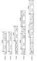
図4は、ISO14443A、ISO15693、ISO18092、ISO18000−6、ISO18000−4の5つのRFID通信規格にそれぞれ定義され、RFIDリーダライタが処理するデータフレームの構成を示す。なお、ISO18000−6とISO18000−4では、RFIDリーダライタが送信するデータフレームと受信するフレームのフォーマットが異なり、図4においてそれぞれ示している。各データフレームにおいて、「CRC」の後の括弧中の数字は、CRCデータのビット数を示す。また、各データフレームの構成要素について、その通信規格で用いられた用語で表記する。 FIG. 4 shows the structure of a data frame defined by five RFID communication standards of ISO14443A, ISO15693, ISO18092, ISO18000-6, and ISO18000-4, and processed by the RFID reader / writer. In ISO 18000-6 and ISO 18000-4, the format of the data frame transmitted from the RFID reader / writer is different from the format of the received frame, which are shown in FIG. In each data frame, the number in parentheses after “CRC” indicates the number of bits of CRC data. In addition, the components of each data frame are expressed in terms used in the communication standard.
図4に示すように、それぞれの通信規格におけるデータフレームは、主として、「Preamble+SYNC+LENGTH」、「SOC」等から構成されるプリアンブルと、データコマンドを含むペイロードと、データコマンドが正しく読みこまれたかどうかを検出(誤り検出)するために用いられるCRCデータと、によって構成される。RFIDリーダライタがRFIDタグからの応答信号(データフレーム)を受信した場合、この応答信号に含まれるプリアンブルに基づいてデータ受信用クロックのタイミングが調整される。そして、このデータ受信用クロックに同期してプリアンブルに続くデータフレームが検出される。 As shown in FIG. 4, the data frame in each communication standard mainly indicates a preamble composed of “Preamble + SYNC + LENGTH”, “SOC”, a payload including a data command, and whether or not the data command has been read correctly. CRC data used for detection (error detection). When the RFID reader / writer receives a response signal (data frame) from the RFID tag, the timing of the data reception clock is adjusted based on the preamble included in the response signal. A data frame following the preamble is detected in synchronization with the data reception clock.
なお、プリアンブルが上位ビットである(すなわち終端データが下位ビットである)か、プリアンブルが下位ビットである(すなわち終端データが上位ビットである)かは、通信規格によって異なる場合がある。しかし、何れの場合おいてもデータフレームの伝送はプリアンブルからである。以下において、データフレームの各構成要素を伝送順に示す。 Note that whether the preamble is the upper bit (that is, the termination data is the lower bit) or whether the preamble is the lower bit (that is, the termination data is the upper bit) may differ depending on the communication standard. However, in any case, the transmission of the data frame is from the preamble. In the following, each component of the data frame is shown in the order of transmission.
図4に示すように、ISO14443Aのデータフレームは、プリアンブル「SOC」と、ペイロードと、16ビットのCRCデータと、終端データ「EOC」からなる。以下、説明上の便宜のため、ペイロードとCRCを合わせてPAYCRCという場合がある。また、PAYCRCは、通常、生成処理に際してエンコードされ、解析処理に際してデコードされる。 As shown in FIG. 4, the ISO 14443A data frame includes a preamble “SOC”, a payload, 16-bit CRC data, and termination data “EOC”. Hereinafter, for convenience of explanation, the payload and CRC may be collectively referred to as PAYCRC. The PAYCRC is normally encoded during the generation process and decoded during the analysis process.
ISO15693のデータフレームは、プリアンブル「SOF」と、PAYCRCと、終端データ「EOF」からなる。CRCデータは16ビットである。 The data frame of ISO15693 includes a preamble “SOF”, PAYCRC, and termination data “EOF”. CRC data is 16 bits.
ISO18092のデータフレームは、プリアンブル「Preamble+SYNC+LENGTH」と、PAYCRCからなる。ISO18092のデータフレームのプリアンブルにおける「SYNC」は、ISO18092のPAYCRCをデコードする際に用いられる極性データ(Polarity Data)が含まれている。また、PAYCRCのデータ長を示す「LENGTH」も、デコードの際に用いられる。ISO18092のデータフレームのCRCデータは16ビットである。ISO18092のデータフレームには、終端データが無い。 A data frame of ISO18092 includes a preamble “Preamble + SYNC + LENGTH” and PAYCRC. “SYNC” in the preamble of the ISO18092 data frame includes polarity data (Polarity Data) used when decoding the ISO18092 PAYCRC. Further, “LENGTH” indicating the data length of the PAYCRC is also used for decoding. The CRC data of the ISO18092 data frame is 16 bits. There is no end data in the ISO18092 data frame.
ISO18000−6では、RFIDリーダライタが送信するデータフレームは、プリアンブルと、PAYCRCからなる。プリアンブルは、「Preamble」と「Framesync」の2種類がある。CRCは、16ビットと5ビットの2種類がある。また、RFIDリーダライタが受信するデータフレームは、プリアンブル「Preamble」とPAYCRCとからなり、CRCは、16ビットである。ISO18000−6のデータフレームも、終端データが無い。 In ISO 18000-6, a data frame transmitted by an RFID reader / writer is composed of a preamble and a PAYCRC. There are two types of preambles, “Preamble” and “Framesync”. There are two types of CRC, 16 bits and 5 bits. A data frame received by the RFID reader / writer is composed of a preamble “Preamble” and PAYCRC, and the CRC is 16 bits. The ISO 18000-6 data frame also has no end data.
ISO18000−4では、RFIDリーダライタが送信するデータフレームは、プリアンブル「Preamble+detect」及び「Preamble+Delimiter」とPAYCRCとからなり、CRCデータは16ビットである。また、RFIDリーダライタが受信するデータフレームは、プリアンブル「Quiet+Preamble」とPAYCRCからなり、CRCデータは16ビットである。ISO18092のデータフレームも、終端データが無い。 In ISO 18000-4, a data frame transmitted by an RFID reader / writer is composed of preambles “Preamble + detect” and “Preamble + Delimiter” and PAYCRC, and CRC data is 16 bits. The data frame received by the RFID reader / writer is composed of a preamble “Quiet + Preamble” and PAYCRC, and the CRC data is 16 bits. The ISO18092 data frame also has no termination data.
また、図4に示していないが、通信規格によって、PAYCRCのデータには、パリティビットが挿入されたものもあれば、パリティビットが挿入されていないものもある。また、通信規格によっては、データコマンドの誤り検出を行う等のために終端データやパリティビットもデータフレームに含まれる場合がある。なお、以下の実施の形態の説明では、いずれの通信規格の場合にも適用可能である。 Although not shown in FIG. 4, depending on the communication standard, some PAYCRC data has a parity bit inserted and some has no parity bit inserted. Also, depending on the communication standard, the end data and the parity bit may be included in the data frame in order to detect an error in the data command. Note that the following description of the embodiment is applicable to any communication standard.
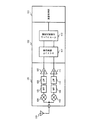
次に、本発明の実施の形態について図面を参照して説明する。図1に、本発明の実施の形態におけるタイミング調整回路112を備えたRFIDリーダライタ(無線タグリーダライタ)を示す。図1に示すRFIDリーダライタは、RFIDタグ(無線タグ)との信号の送受信を行うアンテナ100と、アナログ信号処理を行うRF部101と、デジタル信号処理を行うモデム部102と、CPU等が設けられ所定の演算処理を行う演算処理部103と、を備える。ここで、図1に示すRFIDリーダライタは、データ受信用クロックのタイミング調整に要する時間を短縮し、精度の高いデータ処理を行うことを可能にするタイミング調整回路112を備えることを特徴とする。なお、図1には、RFIDタグからの応答信号を受信する回路のみ示している。したがって、実際には、RFIDタグへの信号を送信するための回路等も備えているが、ここでは説明を省略する。
Next, embodiments of the present invention will be described with reference to the drawings. FIG. 1 shows an RFID reader / writer (wireless tag reader / writer) including a
また、RF部101は、ミキサ104と、HPF(High Pass Filter)105と、LPF(Low Pass Filter)106と、VGA(Variable Gain Amplifier)107と、ミキサ108と、HPF109と、LFP110と、VGA111と、をさらに備える。モデム部102は、タイミング調整回路112と、データフレーム同期検出回路113と、をさらに備える。
The
まず、図1に示す回路の回路構成について説明する。アンテナ100は、ミキサ104の入力端子と、ミキサ108の入力端子と、にそれぞれ接続される。ミキサ104の出力端子は、HPF105の入力端子に接続される。HPF105の出力端子は、LPF106の入力端子に接続される。LPF106の出力端子は、VGA107の入力端子に接続される。VGA107の出力端子は、タイミング調整回路112の一方の入力端子に接続される。
First, the circuit configuration of the circuit shown in FIG. 1 will be described. The
ミキサ108の出力端子は、HPF109の入力端子に接続される。HPF109の出力端子は、LPF110の入力端子に接続される。LPF110の出力端子は、VGA111の入力端子に接続される。VGA111の出力端子は、タイミング調整回路112の他方の入力端子に接続される。
The output terminal of the
タイミング調整回路112の2つの出力端子は、データフレーム同期検出回路113の2つの入力端子に互いに接続される。データフレーム同期検出回路113の出力端子は、演算処理部103の入力端子に接続される。
The two output terminals of the
次に、図1に示す回路の動作について説明する。まず、演算処理部103から出力されたデータフレームは、モデム部102及びRF部101を介してアンテナ100から送信される(不図示)。
Next, the operation of the circuit shown in FIG. 1 will be described. First, the data frame output from the
アンテナ100はRFIDタグからの応答信号を受信する。この応答信号はミキサ104及びミキサ108に入力される。ここでは、ダイレクトコンバージョン方式を採用した例について説明する。すなわち、RFIDタグからの応答信号とRFIDタグに送信する搬送波との位相差により、RFIDタグからの応答信号が検出できなくなるのを回避するため、RFIDタグに送信する搬送波とその位相を90度ずらした信号とでそれぞれ検波する。
The
ミキサ104は、RFIDタグからの応答信号と、RFIDタグに送信する搬送波とをミキシングしてI相ベースバンド信号を出力する。I相ベースバンド信号はHPF105、LPF106によってノイズが取り除かれる。LPF106から出力された信号対は、VGA107によって差動増幅される。
The
同様に、ミキサ108は、RFIDタグからの応答信号と、90度位相がずれた搬送波とをミキシングしてQ相ベースバンド信号を出力する。Q相ベースバンド信号はHPF109、LFP110によってノイズが取り除かれる。LFP110から出力された信号対は、VGA111によって差動増幅される。
Similarly, the
VGA107及びVGA111の出力信号は、タイミング調整回路112に入力される。タイミング調整回路112において、VGA107からの出力信号に含まれるプリアンブルに基づいて受信クロックのタイミングが調整される。同様に、VGA111の出力信号に含まれるプリアンブルに基づいて受信クロックのタイミングが調整される。
Output signals of the
タイミング調整回路112は、VGA107に基づいて調整された受信クロック及びAD変換されたデータフレームと、VGA111に基づいて調整された受信クロック及びAD変換されたデータフレームと、をデータフレーム同期検出回路113に出力する。その後、データフレーム同期検出回路113において、何れかの受信クロック及びデータフレームが選択される。そして、選択された受信クロックによってデータフレームが同期検出され、演算処理部103に送信される。
The
なお、本発明の実施の形態に示すタイミング調整回路112は、趣旨を逸脱しない範囲で適宜変更可能である。例えば、VGA107及びVGA111の出力信号のうち選択された一方のみがタイミング調整回路112に入力される回路構成にも適宜変更可能である。この場合、タイミング調整回路112から出力される信号は、1組の受信クロック及びデータフレームのみである。なお、VGA107及びVGA111の出力信号は、タイミング調整回路112においてそれぞれ同様の処理が行われるため、以下の説明では、VGA107の出力信号の処理についてのみ説明する。
Note that the
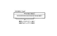
タイミング調整回路112は、VGA107の出力信号(RFIDタグからの応答信号)に含まれるプリアンブルに基づいて、プリアンブルに続くデータフレームを同期検出するための受信クロックのタイミング調整を行う。ここで、図6に通信規格がISO18000−6TypeCのプリアンブルを構成するビットデータの例を示す。図6に示すように、プリアンブルを構成するビットデータは、論理レベルが1ビット毎に反転するビットデータ部分(例えば"1010")を有する。このようなビットデータ部分を用いて、受信用クロックのタイミング調整を行うことがさらに好ましい。なお、以下の説明では、特に断りがない限り、RFIDタグからの応答信号に含まれるプリアンブルであって、論理レベルが1ビット毎に反転するビットデータ部分の信号に基づいてタイミング調整が行われているものとする。
The
次に、図2を用いてタイミング調整回路112についてさらに詳しく説明する。なお、前述のようにRF部101の2つの出力信号(VGA107及びVGA111の出力信号)は、タイミング調整回路112においてそれぞれ同様の処理が行われる。したがって、ここではVGA107の出力信号の処理を行う回路のみについて説明する。
Next, the
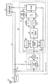
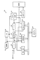
まず、タイミング調整回路112の回路構成について説明する。図2に示すようにタイミング調整回路112は、ADC(A/Dコンバータ)200と、ゼロクロス検出回路201と、受信タイミング決定回路202と、を備える。ゼロクロス検出回路201は、デジタル信号格納部203と、乗算回路204と、を有する。受信タイミング決定回路202は、カウンタ205と、検出結果格納部206と、カウンタ207と、受信タイミング調整部208と、受信タイミング記憶部(第1の受信タイミング記憶部)209と、受信タイミング記憶部(第2の受信タイミング記憶部)210と、セレクタ211と、比較部212と、切替制御部213と、を有する。
First, the circuit configuration of the
RF部101の出力端子(VGA107の出力端子)はADC200の入力端子に接続される。ADC200の出力端子は、デジタル信号格納部203の入力端子と、乗算回路204の一方の入力端子と、データフレーム同期検出回路113のデータ入力端子と、に接続される。ADCクロック(基準クロック)はADC200のクロック入力端子と、デジタル信号格納部203のクロック入力端子と、カウンタ205のクロック入力端子と、カウンタ207のクロック入力端子と、に入力される。デジタル信号格納部203の出力端子は、乗算回路204の他方の入力端子に接続される。
The output terminal of the RF unit 101 (the output terminal of the VGA 107) is connected to the input terminal of the
乗算回路204の出力端子は、検出結果格納部206の一方の入力端子と、カウンタ207の入力端子と、切替制御部213の一方の入力端子と、に接続される。カウンタ205の出力端子は、検出結果格納部206の他方の入力端子に接続される。検出結果格納部206の出力端子は、受信タイミング調整部208の入力端子に接続される。受信タイミング調整部208の出力端子は、受信タイミング記憶部209の入力端子と、受信タイミング記憶部210の入力端子と、に接続される。受信タイミング記憶部209の出力端子は、セレクタ211の一方の入力端子に接続される。受信タイミング記憶部210の出力端子は、セレクタ211の他方の入力端子に接続される。
An output terminal of the
セレクタ211の出力端子は、比較部212の一方の入力端子に接続される。比較部212の一方の出力端子は、データフレーム同期検出回路113のクロック入力端子に接続される。比較部212の他方の出力端子は、切替制御部213の他方の入力端子に接続される。切替制御部213の出力端子は、セレクタ211の切替制御端子に接続される。カウンタ207の出力端子は、比較部212の他方の入力端子に接続される。
The output terminal of the
次に、タイミング調整回路112の動作について説明する。VGA107の出力信号は、ADC200において、ADCクロックに同期してデジタル信号に変換される。図3にADC200の出力結果の例を示す。横軸が時間を示し、縦軸がアナログ信号の電圧に応じたデジタル値を示す。なお、図3中に表されたプロットはADCクロックに同期して変換されたデジタル値を示す。
Next, the operation of the
ADC200の出力信号は、デジタル信号格納部203と、乗算回路204と、データフレーム同期検出回路113と、に入力される。デジタル信号格納部203は、ADC200から出力されたデジタル信号を格納する。乗算回路204は、ADC200においてADCクロックの検出エッジに同期して変換されたデジタル信号と、デジタル信号格納部203に格納された1クロック前のADCクロックの検出エッジに同期して変換されたデジタル信号と、を乗算して出力する。
The output signal of the
このように、乗算回路204において、時間的に隣接して変換された両デジタル信号を乗算することにより、RFIDタグからの応答信号のゼロクロスを検出することが可能である。つまり、両デジタル信号の乗算結果が正の場合には、ゼロクロス検出されない。一方、両デジタル信号の乗算結果が負の場合には、ゼロクロス検出される。そして、乗算回路204の出力信号は、検出結果格納部206の一方の入力端子に入力される。
In this manner, the
カウンタ205は、ADCクロックの検出エッジをカウントする。カウンタ205の出力信号は、検出結果格納部206の他方の入力端子に入力される。検出結果格納部206は、所定の期間(例えば、プリアンブルに含まれる論理レベルが1ビット毎に反転するビットデータ部分の信号の受信期間)、ゼロクロスの検出回数とADCクロックによる検出回数(カウンタ205によるカウント数)とを格納する。そして、検出結果格納部206の出力信号は、受信タイミング調整部208に入力される。
The
受信タイミング調整部208は、ゼロクロスの検出回数とADCクロックによる検出回数とに基づいて、RFIDタグから送信されるプリアンブルの周期を特定する。例えば、ADCクロックが2.6MHz、ゼロクロス検出回数が8回、ADCクロックの検出エッジによる検出回数が320回の場合を考える。ここで、ゼロクロス検出後、次のゼロクロスが検出されるまでを1周期とする。この場合、プリアンブルの周期は65KHzと算出することができる。つまり、ゼロクロス検出後、次のゼロクロスが検出されるまでの間、ADCクロックの検出エッジによる検出回数は平均40回であることがわかる。
The reception
この結果に基づいて、データフレームを同期検出するための受信クロックをタイミング調整することができる。例えば、ゼロクロス検出後、ADCクロックの3クロック目の検出エッジを、受信クロックの検出エッジとしてタイミング調整することができる。 Based on this result, the timing of the reception clock for synchronously detecting the data frame can be adjusted. For example, after zero cross detection, the timing of the detection edge of the third clock of the ADC clock can be adjusted as the detection edge of the reception clock.
受信タイミング調整部208において調整された受信クロックの情報(例えば、ゼロクロスの検出後、ADCクロックの3クロック目を検出エッジとする、という情報)は、受信タイミング記憶部209に入力される。一方、受信タイミング記憶部210には、受信タイミング記憶部209と異なるタイミングに調整された受信クロックの情報(例えば、ADCクロックの6クロック目を検出エッジとする、という情報)が入力される。
Information of the reception clock adjusted by the reception timing adjustment unit 208 (for example, information that the third clock of the ADC clock is detected edge after detection of zero cross) is input to the reception
これは、プリアンブルに続くデータフレームの信号において、同じ論理レベルのビットが連続する場合(例えば"11")を考慮している。例えば、プリアンブルに続くデータフレームの信号において、ゼロクロス検出後、次のゼロクロスが検出されるまで時間が、プリアンブルと比較して2倍であるとする。このとき、ゼロクロスの検出後、例えば、ADCクロックの3クロック目と6クロック目とを検出エッジとすることにより、同じ論理レベルのビットが連続するビットデータをそれぞれ同期検出することができる。 This takes into account the case where bits of the same logic level are consecutive in the data frame signal following the preamble (for example, “11”). For example, in the data frame signal following the preamble, it is assumed that the time after the zero cross is detected until the next zero cross is detected is twice as long as the preamble. At this time, after the zero cross is detected, for example, by setting the third clock and the sixth clock of the ADC clock as detection edges, the bit data in which bits having the same logic level are consecutive can be detected synchronously.
セレクタ211は、受信タイミング記憶部209の出力信号と受信タイミング記憶部210の出力信号とのいずれか一方を選択し、受信タイミング情報として比較部212に出力する。
The
カウンタ207は、乗算回路204からゼロクロスを検出すると、ADCクロックの検出エッジのカウントを開始する。なお、乗算回路204が次のゼロクロスを検出すると、カウント数はリセットされる。
When the
比較部212において、カウンタ207のカウント数と、セレクタ211によって選択された受信タイミング情報と、に基づいてデータフレームを同期検出するための受信クロックを一方の出力端子から出力する。例えば、ゼロクロス検出後、ADCクロックの3クロック目を検出エッジとする場合を考える。この場合、例えば、受信タイミング記憶部209から出力された受信タイミング情報が、セレクタ211を介して比較部212に入力される。ここで、カウンタ207によるカウント数が"3"を示した場合、セレクタ211からの受信タイミング情報と一致して、比較部212から出力される受信クロックが立ち上がる。それにより、データフレーム同期検出回路113において、プリアンブルに続くデータフレームの同期検出を行う。なお、本発明の実施の形態では、受信クロックの検出エッジが立ち上がりエッジの場合を例に説明しているが、立ち下がりエッジの場合にも適宜変更可能である。そして、カウンタ207のカウント数が増加すると、再び受信クロックは立ち下がる。
The
比較部212の他方の出力端子から出力された一致信号(後述)は、切替制御部213に入力される。また、乗算回路204の出力信号も切替制御部213に入力される。切替制御部213は、これらの信号に基づいて、セレクタ211の出力信号を選択的に切り替える。
A coincidence signal (described later) output from the other output terminal of the
具体的には、例えば、切替制御部213は、乗算回路204からゼロクロスを検出すると、比較部212から出力される一致信号のカウントを開始する。ここで、一致信号とは、セレクタ211から出力される受信タイミング情報と、カウンタ207のカウント数とが一致した場合に、比較部212から出力される信号のことである。なお、比較部212の一方の出力端子から出力される受信クロックの検出エッジ(例えば、立ち上がりエッジ)を一致信号として用いても良い。初期状態においてカウント数が"0"を示す場合、切替制御部213は例えばロウレベルの信号をセレクタ211の切替制御端子に出力する。それにより、セレクタ211は、受信タイミング記憶部209の出力信号を選択する。一方、比較部212から出力される一致信号により、カウント数が"1"を示す場合、切替制御部213は例えばハイレベルの信号をセレクタ211の切替制御端子に出力する。それにより、セレクタ211は、受信タイミング記憶部210の出力信号を選択する。なお、乗算回路204が次のゼロクロスを検出すると、カウント数はリセットされる。
Specifically, for example, when the switching
このように、受信タイミング情報を切り替えることにより、プリアンブルに続くデータフレームにおいて、同じ論理レベルのビットが連続するビットデータを同期検出することができる。 In this way, by switching the reception timing information, it is possible to synchronously detect bit data in which bits having the same logic level are continuous in the data frame following the preamble.
以上のように、本発明の実施の形態にかかるタイミング調整回路は、データフレーム用の受信クロックのタイミング調整のためにマイクロプロセッサ等の演算回路を使用しない。したがって、タイミング調整に要する時間を短縮することができる。近年のデータ通信速度の向上に対応して、タイミング調整の遅れを抑制することができるため、精度の高いデータ処理を可能にすることができる。また、本発明の実施の形態にかかるタイミング調整回路は、PLL等の大規模回路によるタイミング調整を行わないため、回路規模の増大を抑制することができる。 As described above, the timing adjustment circuit according to the embodiment of the present invention does not use an arithmetic circuit such as a microprocessor for timing adjustment of the reception clock for the data frame. Therefore, the time required for timing adjustment can be shortened. Corresponding to the recent increase in data communication speed, it is possible to suppress delays in timing adjustment, thereby enabling highly accurate data processing. Moreover, since the timing adjustment circuit according to the embodiment of the present invention does not perform timing adjustment by a large-scale circuit such as a PLL, an increase in circuit scale can be suppressed.
なお、本発明は上記実施の形態に限られたものではなく、趣旨を逸脱しない範囲で適宜変更することが可能である。例えば、本発明の実施の形態のRFIDリーダライタでは、モデム部102に備えられた受信回路として、タイミング調整回路112と、データフレーム同期検出回路113と、が備えられた場合の例について説明したが、これに限られない。例えば、データフレームのノイズを除去するためのローパスフィルター回路等が備えられた回路構成にも適宜変更可能である。
Note that the present invention is not limited to the above-described embodiment, and can be changed as appropriate without departing from the spirit of the present invention. For example, in the RFID reader / writer according to the embodiment of the present invention, an example in which the
また、本発明の実施の形態では、RFIDリーダライタにおいて、RFIDタグからの応答信号によってI相ベースバンド信号とQ相ベースバンド信号の2種類の信号が生成される場合の例について説明したが、これに限られない。例えば、I相ベースバンド信号のみが生成される回路構成にも適宜変更することが可能である。あるいは、趣旨を逸脱しない限りにおいて、RFIDタグからの応答信号を受信する方式として、ダイレクトコンバージョン方式に代わる他の方式(例えば、スーパーヘテロダイン方式)を用いても良い。 In the embodiment of the present invention, an example in which two types of signals of an I-phase baseband signal and a Q-phase baseband signal are generated by a response signal from the RFID tag in the RFID reader / writer has been described. It is not limited to this. For example, the circuit configuration in which only the I-phase baseband signal is generated can be appropriately changed. Alternatively, as long as it does not depart from the spirit, another method (for example, superheterodyne method) instead of the direct conversion method may be used as a method for receiving a response signal from the RFID tag.
また、本発明の実施の形態にかかるタイミング調整回路112は、図2に示す回路に限られず、趣旨を逸脱しない限りにおいて適宜変更が可能である。例えば、図2に示す回路は、受信タイミング情報を格納する受信タイミング記憶部が2個の場合について説明したがこれに限られない。プリアンブルに続くデータフレームを同期検出するために、必要であれば3個以上の受信タイミング記憶部を備えた回路構成にも適宜変更可能である。あるいは、不要であれば受信タイミング記憶部を備えない回路構成にも適宜変更可能である。この場合、受信タイミング調整部208から出力される受信タイミング情報が直接比較部212に入力される。
Further, the
100 アンテナ
101 RF部
102 モデム部
103 演算処理部
104 ミキサ
105 HPF
106 LPF
107 VGA
108 ミキサ
109 HPF
110 LPF
111 VGA
112 タイミング調整回路
113 データフレーム同期検出回路
200 ADC
201 ゼロクロス検出回路
202 受信タイミング決定回路
203 デジタル信号格納部
204 乗算回路
205 カウンタ
206 検出結果格納部
207 カウンタ
208 受信タイミング調整部
209 受信タイミング記憶部
210 受信タイミング記憶部
211 セレクタ
212 比較部
213 切替制御部
DESCRIPTION OF
106 LPF
107 VGA
108
110 LPF
111 VGA
112
DESCRIPTION OF
Claims (8)
前記送信信号のプリアンブルを構成するアナログ信号を、基準クロックに基づいてデジタル信号に変換するA/Dコンバータと、
前記A/Dコンバータにより変換された第1のデジタル信号と、当該第1のデジタル信号と時間的に隣接して変換された第2のデジタル信号と、からゼロクロスを検出するゼロクロス検出回路と、
前記基準クロックと前記ゼロクロスの検出回数とに基づいて前記受信タイミングを決定する受信タイミング決定回路と、を備えたタイミング調整回路。 A timing adjustment circuit for adjusting a reception timing of a transmission signal transmitted from a wireless tag,
An A / D converter that converts an analog signal constituting a preamble of the transmission signal into a digital signal based on a reference clock;
A zero cross detection circuit for detecting a zero cross from the first digital signal converted by the A / D converter and the second digital signal converted in time adjacent to the first digital signal;
A timing adjustment circuit comprising: a reception timing determination circuit that determines the reception timing based on the reference clock and the number of times of detection of the zero cross.
前記第1のデジタル信号を格納するデジタル信号格納部と、
当該第1のデジタル信号と前記第2のデジタル信号とを乗算する乗算回路と、を備えた請求項1又は2に記載のタイミング調整回路。 The zero cross detection circuit
A digital signal storage unit for storing the first digital signal;
The timing adjustment circuit according to claim 1, further comprising a multiplication circuit that multiplies the first digital signal and the second digital signal.
前記基準クロックの検出エッジをカウントするカウンタを備え、
前記カウンタのカウント数と前記ゼロクロスの検出回数とに基づいて前記受信タイミングを決定することを特徴とする請求項1〜3のいずれか一項に記載のタイミング調整回路。 The reception timing determination circuit includes:
A counter that counts the detection edges of the reference clock;
The timing adjustment circuit according to any one of claims 1 to 3, wherein the reception timing is determined based on a count number of the counter and a number of times of detection of the zero cross.
前記カウンタのカウント数と前記ゼロクロスの検出回数とに基づいて第1の受信タイミング情報を記憶する第1の受信タイミング記憶部と、
前記第1の受信タイミング情報と異なる第2の受信タイミング情報を記憶する第2の受信タイミング記憶部と、
前記プリアンブルに続くデータパタンに応じて前記第1の受信タイミング情報と前記第2の受信タイミング情報のいずれかを選択するセレクタと、
前記ゼロクロス検出後の経過時間と、前記セレクタから出力される前記第1又は第2の受信タイミング情報と、に基づいて受信タイミングを決定する比較部と、を備えた請求項1〜4のいずれか一項に記載のタイミング調整回路。 The reception timing determination circuit includes:
A first reception timing storage unit that stores first reception timing information based on the count number of the counter and the number of times of detection of the zero cross,
A second reception timing storage unit for storing second reception timing information different from the first reception timing information;
A selector that selects one of the first reception timing information and the second reception timing information according to a data pattern following the preamble;
The comparison part which determines reception timing based on the elapsed time after the said zero cross detection, and the said 1st or 2nd reception timing information output from the said selector, The any one of Claims 1-4 The timing adjustment circuit according to one item.
前記送信信号のプリアンブルを構成するアナログ信号を、基準クロックに基づいてデジタル信号に変換し、
変換された第1のデジタル信号と、当該第1のデジタル信号と時間的に隣接して変換された第2のデジタル信号と、からゼロクロスを検出し、
前記基準クロックと前記ゼロクロスの検出回数とに基づいて前記受信タイミングを決定するタイミング調整回路の調整方法。 A timing adjustment circuit for adjusting a reception timing of a transmission signal transmitted from a wireless tag,
An analog signal constituting a preamble of the transmission signal is converted into a digital signal based on a reference clock;
Detecting a zero cross from the converted first digital signal and the second digital signal converted in time adjacent to the first digital signal;
An adjustment method of a timing adjustment circuit that determines the reception timing based on the reference clock and the number of times of detection of the zero cross.
Priority Applications (1)
| Application Number | Priority Date | Filing Date | Title |
|---|---|---|---|
| JP2009045332A JP2010200220A (en) | 2009-02-27 | 2009-02-27 | Timing adjustment circuit, and method of adjusting the same |
Applications Claiming Priority (1)
| Application Number | Priority Date | Filing Date | Title |
|---|---|---|---|
| JP2009045332A JP2010200220A (en) | 2009-02-27 | 2009-02-27 | Timing adjustment circuit, and method of adjusting the same |
Publications (1)
| Publication Number | Publication Date |
|---|---|
| JP2010200220A true JP2010200220A (en) | 2010-09-09 |
Family
ID=42824427
Family Applications (1)
| Application Number | Title | Priority Date | Filing Date |
|---|---|---|---|
| JP2009045332A Pending JP2010200220A (en) | 2009-02-27 | 2009-02-27 | Timing adjustment circuit, and method of adjusting the same |
Country Status (1)
| Country | Link |
|---|---|
| JP (1) | JP2010200220A (en) |
Cited By (4)
| Publication number | Priority date | Publication date | Assignee | Title |
|---|---|---|---|---|
| US10225068B2 (en) | 2016-10-28 | 2019-03-05 | Fujitsu Limited | Clock recovery circuit, semiconductor integrated circuit device and radio frequency tag |
| CN112654082A (en) * | 2019-10-11 | 2021-04-13 | 广东博智林机器人有限公司 | Timing device, base station, positioning system, calibration method and positioning method |
| CN115811325A (en) * | 2022-10-31 | 2023-03-17 | 深圳市锐能微科技有限公司 | UART serial communication circuit and output method of voltage zero-crossing signal |
| WO2025182164A1 (en) * | 2024-02-28 | 2025-09-04 | パイクリスタル株式会社 | Wireless tag, communication terminal, communication system, and communication method |
Citations (3)
| Publication number | Priority date | Publication date | Assignee | Title |
|---|---|---|---|---|
| JP2001175825A (en) * | 1999-12-20 | 2001-06-29 | Sony Corp | Information processing device, IC card and reader / writer |
| JP2002101140A (en) * | 2000-09-22 | 2002-04-05 | Hitachi Kokusai Electric Inc | Demodulation method |
| JP2003234791A (en) * | 2002-02-07 | 2003-08-22 | Hitachi Kokusai Electric Inc | Symbol timing detection method |
-
2009
- 2009-02-27 JP JP2009045332A patent/JP2010200220A/en active Pending
Patent Citations (3)
| Publication number | Priority date | Publication date | Assignee | Title |
|---|---|---|---|---|
| JP2001175825A (en) * | 1999-12-20 | 2001-06-29 | Sony Corp | Information processing device, IC card and reader / writer |
| JP2002101140A (en) * | 2000-09-22 | 2002-04-05 | Hitachi Kokusai Electric Inc | Demodulation method |
| JP2003234791A (en) * | 2002-02-07 | 2003-08-22 | Hitachi Kokusai Electric Inc | Symbol timing detection method |
Cited By (5)
| Publication number | Priority date | Publication date | Assignee | Title |
|---|---|---|---|---|
| US10225068B2 (en) | 2016-10-28 | 2019-03-05 | Fujitsu Limited | Clock recovery circuit, semiconductor integrated circuit device and radio frequency tag |
| CN112654082A (en) * | 2019-10-11 | 2021-04-13 | 广东博智林机器人有限公司 | Timing device, base station, positioning system, calibration method and positioning method |
| CN112654082B (en) * | 2019-10-11 | 2023-02-24 | 广东博智林机器人有限公司 | Timing device, base station, positioning system, calibration method and positioning method |
| CN115811325A (en) * | 2022-10-31 | 2023-03-17 | 深圳市锐能微科技有限公司 | UART serial communication circuit and output method of voltage zero-crossing signal |
| WO2025182164A1 (en) * | 2024-02-28 | 2025-09-04 | パイクリスタル株式会社 | Wireless tag, communication terminal, communication system, and communication method |
Similar Documents
| Publication | Publication Date | Title |
|---|---|---|
| JP5225816B2 (en) | Semiconductor device | |
| US20170155458A1 (en) | Multi-lane synchronization method, synchronization apparatus and system, and computer storage medium | |
| CN105049069B (en) | Symbol clock recovery circuit | |
| US8125258B2 (en) | Phase synchronization device and phase synchronization method | |
| JP2010200220A (en) | Timing adjustment circuit, and method of adjusting the same | |
| EP4142204B1 (en) | Wireless audio synchronization method, wireless audio playback device and wireless audio transceiving system | |
| JP6022843B2 (en) | Wireless communication apparatus and received signal processing method | |
| JP4728373B2 (en) | Wireless communication system, receiver, and transmitter | |
| US5598446A (en) | Clock extraction of a clock signal using rising and falling edges of a received transmission signal | |
| US9094911B2 (en) | Data communication system, method of optimizing preamble length, and communication apparatus | |
| US8199869B2 (en) | Communication apparatus | |
| US5907558A (en) | Burst signal reception method and apparatus | |
| JP3412558B2 (en) | Clock frequency control method and receiving device used therefor | |
| JP7709079B2 (en) | Receiver and correction method | |
| JP3176801B2 (en) | Synchronization device | |
| JP2008283634A (en) | Demodulation circuit and rfid system | |
| JP4952488B2 (en) | Synchronous tracking circuit | |
| US8073082B2 (en) | Mirror sub-carrier demodulation circuit, receiving device with the same, and mirror sub-carrier demodulating method | |
| JP2004146987A (en) | Received data reproducing apparatus | |
| JP2002237807A (en) | Frame synchronous signal detecting system | |
| JP3039497B2 (en) | Clock extraction circuit, communication system, and transmission device | |
| KR101092850B1 (en) | Clock frequency offset compensation method and apparatus for base station and terminal communication system | |
| JP2010199912A (en) | Preamble detection circuit, and detection method therein | |
| JP2003188931A (en) | Clock recovery device and clock recovery method | |
| JP4434429B2 (en) | Symbol identification timing generator, receiving apparatus and communication apparatus using the same |
Legal Events
| Date | Code | Title | Description |
|---|---|---|---|
| A621 | Written request for application examination |
Free format text: JAPANESE INTERMEDIATE CODE: A621 Effective date: 20110228 |
|
| A977 | Report on retrieval |
Free format text: JAPANESE INTERMEDIATE CODE: A971007 Effective date: 20121119 |
|
| A131 | Notification of reasons for refusal |
Free format text: JAPANESE INTERMEDIATE CODE: A131 Effective date: 20121127 |
|
| A02 | Decision of refusal |
Free format text: JAPANESE INTERMEDIATE CODE: A02 Effective date: 20130319 |