JP2010157504A - Radio frequency output transition portion suitable for high power microwave electron tube - Google Patents
Radio frequency output transition portion suitable for high power microwave electron tube Download PDFInfo
- Publication number
- JP2010157504A JP2010157504A JP2009291037A JP2009291037A JP2010157504A JP 2010157504 A JP2010157504 A JP 2010157504A JP 2009291037 A JP2009291037 A JP 2009291037A JP 2009291037 A JP2009291037 A JP 2009291037A JP 2010157504 A JP2010157504 A JP 2010157504A
- Authority
- JP
- Japan
- Prior art keywords
- transition
- curvature
- microwave
- rectangular
- tube
- Prior art date
- Legal status (The legal status is an assumption and is not a legal conclusion. Google has not performed a legal analysis and makes no representation as to the accuracy of the status listed.)
- Granted
Links
- 230000007704 transition Effects 0.000 title claims abstract description 100
- 230000002457 bidirectional effect Effects 0.000 claims abstract description 7
- 230000001902 propagating effect Effects 0.000 claims abstract description 3
- 238000000926 separation method Methods 0.000 claims description 10
- 230000005684 electric field Effects 0.000 abstract description 13
- 239000007789 gas Substances 0.000 description 22
- 230000015556 catabolic process Effects 0.000 description 15
- IJGRMHOSHXDMSA-UHFFFAOYSA-N Atomic nitrogen Chemical compound N#N IJGRMHOSHXDMSA-UHFFFAOYSA-N 0.000 description 8
- 238000010894 electron beam technology Methods 0.000 description 4
- 238000012423 maintenance Methods 0.000 description 4
- 229910052757 nitrogen Inorganic materials 0.000 description 4
- 238000010586 diagram Methods 0.000 description 3
- 230000000694 effects Effects 0.000 description 2
- 238000010891 electric arc Methods 0.000 description 2
- 239000005431 greenhouse gas Substances 0.000 description 2
- 238000007789 sealing Methods 0.000 description 2
- 229910018503 SF6 Inorganic materials 0.000 description 1
- 230000003321 amplification Effects 0.000 description 1
- 238000005219 brazing Methods 0.000 description 1
- 239000000919 ceramic Substances 0.000 description 1
- 230000000593 degrading effect Effects 0.000 description 1
- 230000005672 electromagnetic field Effects 0.000 description 1
- 230000003993 interaction Effects 0.000 description 1
- 239000000463 material Substances 0.000 description 1
- 238000005259 measurement Methods 0.000 description 1
- 238000000034 method Methods 0.000 description 1
- 238000003199 nucleic acid amplification method Methods 0.000 description 1
- 239000002245 particle Substances 0.000 description 1
- SFZCNBIFKDRMGX-UHFFFAOYSA-N sulfur hexafluoride Chemical compound FS(F)(F)(F)(F)F SFZCNBIFKDRMGX-UHFFFAOYSA-N 0.000 description 1
- 229960000909 sulfur hexafluoride Drugs 0.000 description 1
- 230000001960 triggered effect Effects 0.000 description 1
Images
Classifications
-
- H—ELECTRICITY
- H01—ELECTRIC ELEMENTS
- H01J—ELECTRIC DISCHARGE TUBES OR DISCHARGE LAMPS
- H01J23/00—Details of transit-time tubes of the types covered by group H01J25/00
- H01J23/12—Vessels; Containers
-
- H—ELECTRICITY
- H01—ELECTRIC ELEMENTS
- H01J—ELECTRIC DISCHARGE TUBES OR DISCHARGE LAMPS
- H01J23/00—Details of transit-time tubes of the types covered by group H01J25/00
- H01J23/36—Coupling devices having distributed capacitance and inductance, structurally associated with the tube, for introducing or removing wave energy
Landscapes
- Microwave Tubes (AREA)
- Waveguides (AREA)
- Physical Or Chemical Processes And Apparatus (AREA)
Abstract
Description
本発明は、高出力マイクロ波管の無線周波数出力部と導波管との間の遷移部に関する。 The present invention relates to a transition between a radio frequency output of a high power microwave tube and a waveguide.
高出力マイクロ波電子管、例えばL帯、すなわち1〜2GHzの周波数帯域で動作するクライストロンなどは、少なくとも1つの高出力のRF出力部を備え、それを導波管に接続して、管によって供給されるRF電力を、マイクロ波を使用する回路へ伝送する。 High-power microwave electron tubes, such as klystrons operating in the L-band, ie 1-2 GHz frequency band, are provided with at least one high-power RF output, connected to the waveguide and supplied by the tube RF power transmitted to a circuit using microwaves.
クライストロンの出力空洞を、電磁波を透過するマイクロ波窓を介して導波管に接続する。マイクロ波窓は、真空下にある管の内側を、おそらくガス圧力下にある外側から隔離する。さらに、円形のシリンダー形状である窓の出力部を矩形断面の導波管に接続するために、マイクロ波窓の後段に遷移部が必要となる。 The output cavity of the klystron is connected to the waveguide through a microwave window that transmits electromagnetic waves. The microwave window isolates the inside of the tube under vacuum from the outside, possibly under gas pressure. Furthermore, in order to connect the output portion of the window having a circular cylinder shape to the waveguide having a rectangular cross section, a transition portion is required after the microwave window.
従来のクライストロンは、本質的に、管のRF入力部に適用されるマイクロ波を増幅するための、マイクロ波構造を有する増幅器である。増幅は、前記構造を通過する1つ以上の電子ビームの運動エネルギーを電磁エネルギーに変換することによって行われる。 A conventional klystron is essentially an amplifier having a microwave structure for amplifying the microwave applied to the RF input of the tube. Amplification is performed by converting the kinetic energy of one or more electron beams passing through the structure into electromagnetic energy.
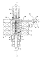
図1に、縦軸XX’に沿って真空室10を含む従来技術の単一ビームのクライストロンの概略図を示し、クライストロンは、
−連続またはパルス電子ビーム24を放射する、バイアスされたカソード22を備える電子銃20であって、電子が、XX’軸に沿ってアノード26によって加速される、電子銃20と、
−無線周波数(RF)信号が管のRF入力部28を介して注入されるときにビームの電子密度を変更するための入力共振空洞C1と、
−永久磁石からまたはソレノイド32によって生じた電子ビームをXX’軸に沿って集束させる(または閉じ込める)ための回路30と、
−電子ビームの電子44を集めるための電子コレクタ40であって、管のカソード22によって放射された電子のほとんどを受け取りかつ電子がマイクロ波構造を通過した後にそれらの残留運動エネルギーを消散させることを可能とする電子コレクタ40と、
−アノード26と電子コレクタ40との間に配置される共振回路50であって、共振回路にあるビーム中の電子の運動エネルギーの一部を、回路の共振周波数でRFエネルギーに変換する機能を有する共振回路50と
を備える。共振回路50は相互作用構造とも称す。共振回路はクライストロンの一体部分を形成し、かつマイクロ波構造に一連の共振空洞C1、C2、C3、C4...を備える。
FIG. 1 shows a schematic diagram of a prior art single beam klystron including a
An
An input resonant cavity C1 for changing the electron density of the beam when a radio frequency (RF) signal is injected through the
A
An
A
クライストロンはさらに、管の外側に対して、増幅されたRF電力を抽出するための出力遷移部60に接続された導波管の形態の少なくとも1つのRF電力出力部58を含む。
The klystron further includes at least one
クライストロンのこの実施形態では、出力遷移部60は、真空下の管の内側とガス圧力下の適用導波管(図1には図示せず)との間を封止するセラミック窓61と、フランジ64による導波管への接続部とを含む。
In this embodiment of the klystron, the
高出力電力のクライストロンの場合、例えばL帯において使用される導波管は、矩形断面のWR650導波管である。 In the case of a high output power klystron, for example, the waveguide used in the L band is a WR650 waveguide having a rectangular cross section.
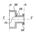
図2に、図1に示すクライストロンの従来技術の出力遷移部の部分的な図(B−Bの図)を示す。 FIG. 2 shows a partial view (BB diagram) of the output transition part of the prior art of the klystron shown in FIG.
出力遷移部60は、クライストロンの出力側に、別個の窓(図2には図示せず)を介して、クライストロンの出力部に接続された円形断面のシリンダー状部分66と、その対向する側に、適用導波管に接続するためのフランジ64を含む矩形断面の管の形態の別の部分68とを含む。遷移部の内部では、シリンダー状面および矩形セクションの各平面が、半径rの隅肉部70によって接合している。
The
マイクロ波出力回路は、高出力クライストロンによる、とりわけ出力遷移部60におけるRF電力出力部を通過することによって、強電界にさらされる。出力遷移部におけるRF電力波によって生じた電界が、遷移部の一定の箇所(または電極)間に前記遷移部の絶縁破壊電圧超の電圧を生じる場合、電気アークが生じ、それによりクライストロンを劣化させる。
The microwave output circuit is exposed to a strong electric field by passing through the RF power output section at the
クライストロンの出力部にはアーク検出器を含むが、これらの検出器は絶縁破壊発生時にのみ迅速にトリガされ得、それでもなお、時間と共にアークの挙動を制限する。 Although the output of the klystron includes arc detectors, these detectors can only be triggered quickly only when a breakdown occurs and still limit the arc behavior over time.
クライストロンの出力回路の絶縁破壊抵抗は、例えば出力回路における定在波比、RF信号の調波、遷移部および導波管の温度など様々なパラメータ、ならびに、例えば測定部品またはカプラーなどの出力回路に存在する他の要素の影響の他、アーク発生抵抗を低減する、加圧回路のガス中に浮遊している粒子などにも依存する。 The breakdown resistance of the output circuit of the klystron is determined by various parameters such as the standing wave ratio in the output circuit, the harmonics of the RF signal, the temperature of the transition part and the waveguide, and the output circuit such as the measurement component or coupler In addition to the effects of other elements present, it also depends on the particles suspended in the gas of the pressurized circuit, which reduces arcing resistance.
管のRF出力回路においてアークが発生しないようにするためには、臨界絶縁破壊閾値を超えないようにすることが重要である。この限界値に対応する出力回路における電界は、電気強度またはガスの絶縁破壊強度と称されるものである。この絶縁破壊強度は、アークを生じる傾向のある出力回路の部分(電極に等しい)と回路のそれらの部分の材料との間の距離が乗算されたガス圧力に依存する。 In order to prevent arcing in the tube RF output circuit, it is important not to exceed the critical breakdown threshold. The electric field in the output circuit corresponding to this limit value is referred to as electric strength or gas breakdown strength. This breakdown strength depends on the gas pressure multiplied by the distance between the parts of the output circuit that are prone to arcing (equal to the electrodes) and the material of those parts of the circuit.
概して、アークは特に管の出力部を遷移部内部の導波管に接続する遷移部の、遷移部のシリンダー状部分66と矩形部分68との間の隅肉部70において生じる。図2に示す従来技術のこのタイプの遷移部の欠点の1つは、このゾーンのジオメトリのために電界が局所的に増大する領域を有し、電界が絶縁破壊閾値を局所的に超え得ることである。遷移部の電磁場が、隅肉部70の中心部分において最大レベルに達する。
In general, the arc occurs at the
従来技術のこのタイプの遷移部の電気アーク抵抗は、L帯において、シリンダー状部分66の内面と矩形部分68の内面との間の隅肉部が小半径r、例えば約2〜3mmであるため、制限される。
The electric arc resistance of this type of transition of the prior art is that in the L band, the fillet between the inner surface of the
電磁波が伝わる閉鎖容積部における絶縁破壊閾値は、使用されるガスの組成だけでなく、圧力にも依存する。空気が乾燥している場合、1kV/mmのオーダーの最大電界がRF電力回路において通例である。 The dielectric breakdown threshold in the closed volume where electromagnetic waves are transmitted depends not only on the composition of the gas used but also on the pressure. When the air is dry, a maximum electric field on the order of 1 kV / mm is common in RF power circuits.
例えば、特定の電力条件下および周波数条件下において、遷移部の電界は、局所的に導波管の電界の2倍になり得る。その結果、遷移部は、絶縁破壊の危険性があるために伝達され得るRF電力を制限するマイクロ波回路の要素となる。 For example, under certain power and frequency conditions, the electric field at the transition can locally be twice that of the waveguide. As a result, the transition becomes an element of a microwave circuit that limits the RF power that can be transmitted due to the risk of breakdown.
従来技術のこのタイプの遷移部の絶縁破壊閾値を高くするための一解決法は、遷移部および適用導波管において圧力下で六フッ化硫黄すなわちSF6などのガスを使用することからなる。 One solution for increasing the breakdown threshold of this type of transition in the prior art consists of using a gas such as sulfur hexafluoride or SF 6 under pressure in the transition and the applied waveguide.
マイクロ波遷移部60および適用導波管はSF6または等価のタイプのガスで加圧される必要がある。このタイプのSF6ガスを用いた加圧によって、クライストロンからの最大出力電力を伝達することが可能となり、それは、空気または窒素によって加圧する場合よりも遥かに高い。
The
しかしながら、加圧のためにSF6ガスを使用することには欠点がある。特に、SF6は温室効果ガスであり、出力回路を加圧するかまたは減圧する出力回路の保守には、ガスの一部が大気中に逃げないようにするための予防措置が必要となる。 However, the use of SF 6 gas for pressurization has drawbacks. In particular, SF 6 is a greenhouse gas, and maintenance of the output circuit that pressurizes or depressurizes the output circuit requires precautions to prevent part of the gas from escaping into the atmosphere.
クライストロンの出力回路中のガスを収集するためにボトルを使用すること、およびこのような欠点を有しない別のガスで回路を加圧することによってこの回路のドレーニングを行うことなど、大気中にこのガスが漏出しないようにするために相当な手順を考慮する必要がある。 This gas in the atmosphere, such as using a bottle to collect the gas in the output circuit of the klystron and draining this circuit by pressurizing the circuit with another gas that does not have such disadvantages Considerable procedures must be taken into account to prevent leakage.
さらに、ガスSF6は、純粋であればヒトには無害であるが、出力回路で使用された後に置換されると有害となる可能性がある。これは、RF出力回路における繰り返し絶縁破壊が、初期の純粋なSF6ガスが分解するために、有害な他のガスを生じるためである。 Furthermore, the gas SF 6 is harmless to humans if pure, but can be harmful if replaced after being used in the output circuit. This is because repeated breakdown in the RF output circuit produces other harmful gases as the initial pure SF 6 gas decomposes.
従来技術のマイクロ波電力遷移部の欠点を軽減するために、本発明は、縦軸ZZ’に沿った、2つの端部を有する管形状の本体と、2つの端部間に、電磁波を伝播させる内面を有する通路とを備える、高出力電子管用のマイクロ波出力遷移部であって、円形のシリンダー状管の形態の端部の一方は円錐状内側伝播面を有し、矩形断面の管の形態の他方の端部は、2つの長い側面と、長い側面に対して垂直な2つの短い側面とを有し、通路は、長い側面に対して平行な2つの平面的な内側伝播面と、短い側面に対して平行な2つの他の平面的な内面とを有するマイクロ波出力遷移部において、
長い側面に対して平行な平面的な内側伝播面の各々が、双方向性の曲率半径を有する各接続曲面を介して円錐状内側伝播面に接合されることを特徴とするマイクロ波出力遷移部を提供する。
In order to alleviate the disadvantages of the prior art microwave power transition, the present invention propagates electromagnetic waves between two ends and a tube-shaped body having two ends along the longitudinal axis ZZ ′. A microwave power transition for a high power electron tube, wherein one of the ends in the form of a circular cylindrical tube has a conical inner propagation surface, The other end of the form has two long sides and two short sides perpendicular to the long side, and the passage is two planar inner propagation surfaces parallel to the long side; In a microwave power transition having two other planar inner surfaces parallel to the short side,
Each of the planar inner propagation surfaces parallel to the long side surface is joined to the conical inner propagation surface via each connecting curved surface having a bidirectional radius of curvature. I will provide a.
双方向性の曲率半径が可変長であることが有利である。 Advantageously, the bidirectional radius of curvature is of variable length.
一実施形態では、双方向性の曲率半径は、本体の矩形端部の短い側面に対して平行な各回転軸の周りを回転する水平曲率半径と、本体の前記矩形端部の長い側面に対して平行な各回転軸の周りを回転する垂直曲率半径とを有する。 In one embodiment, the bi-directional radius of curvature is relative to the horizontal radius of curvature that rotates about each axis of rotation parallel to the short side of the rectangular end of the body and the long side of the rectangular end of the body. And a vertical radius of curvature that rotates about each parallel axis of rotation.
別の実施形態では、長い側面に対して平行な平面的な内側伝播面を円錐状内側伝播面に接続するための2つの曲面は、ZZ’軸の両側において対称的である。 In another embodiment, the two curved surfaces for connecting the planar inner propagation surface parallel to the long side to the conical inner propagation surface are symmetrical on both sides of the ZZ 'axis.
別の実施形態では、本体のZZ’軸を通る平面における垂直曲率半径Rvcは、矩形セクションの短い側面の平面的な内面を通る、矩形端部の長い側面に対して垂直なその各平面における第1の垂直曲率半径Rv1または最後の垂直曲率半径Rvpよりも大きく、同じ値であるこれらの第1の垂直曲率半径または最後の垂直曲率半径は、矩形端部の長い側面に対して平行な内面と接続するための2つの内面の垂直曲率半径の中で最も小さい。 In another embodiment, the vertical radius of curvature Rvc in a plane through the ZZ ′ axis of the body passes through the planar inner surface of the short side of the rectangular section and is the first in each plane perpendicular to the long side of the rectangular end. These first vertical radius of curvature or last vertical radius of curvature greater than or equal to one vertical radius of curvature Rv1 or the last vertical radius of curvature Rvp are defined by an inner surface parallel to the long side of the rectangular end. The smallest of the vertical curvature radii of the two inner surfaces for connection.
別の実施形態では、遷移部の本体は、矩形断面の管の形態の端部と円形のシリンダー状管の形態の端部との間に中心部分を含み、前記中心部分は、周囲媒体と接触する外面、すなわち一方では、本体の矩形端部の長い側面に対して平行なZZ’軸を通る平面に対して対称的である各傾斜平面における2つの平面的な外側接続面、他方では、ZZ’軸を通る別の平面の両側において対称的でありかつ遷移部の矩形端部の短い側面に対して平行な2つの他の平面的な外側接続面を有する。 In another embodiment, the body of the transition includes a central portion between an end in the form of a rectangular cross-section tube and an end in the form of a circular cylindrical tube, the central portion being in contact with the surrounding medium Two planar outer connecting surfaces in each inclined plane that are symmetrical with respect to a plane passing through the ZZ ′ axis parallel to the long side of the rectangular end of the body, on the one hand, on the other hand, ZZ 'Has two other planar outer connecting surfaces that are symmetrical on both sides of another plane passing through the axis and parallel to the short side of the rectangular end of the transition.
特定の別の実施形態では、遷移部の本体の寸法は、
−ZZ’軸に沿って長さL=99mm、
−円形端部の直径D=205mm、
−円錐状内面の円錐の頂角θ=135°、
−矩形端部の内部矩形セクションの高さH=82mmおよび幅L=165mm、
−ZZ’軸に対して垂直でありかつこの軸を通る平面P3における垂直曲率半径Rvcは60mm
である。
In certain other embodiments, the dimensions of the transition body are:
A length L = 99 mm along the ZZ ′ axis,
The diameter D of the circular end D = 205 mm,
The apex angle of the cone of the conical inner surface θ = 135 °,
The height H = 82 mm and the width L = 165 mm of the inner rectangular section at the rectangular end,
The perpendicular curvature radius Rvc in the plane P3 perpendicular to the −ZZ ′ axis and passing through this axis is 60 mm.
It is.
別の実施形態では、遷移部は、本体の矩形端部に固定された接続フランジと、前記本体の円形端部に固定された円形のシリンダー状分離窓とを含む。 In another embodiment, the transition includes a connection flange secured to the rectangular end of the body and a circular cylindrical separation window secured to the circular end of the body.
本発明はまた、本発明によるRF出力遷移部を備えることを特徴とする、クライストロンおよびTWTから選択された電子管、または他の高出力マイクロ波管に関する。 The invention also relates to an electron tube selected from klystrons and TWTs, or other high-power microwave tubes, characterized in that it comprises an RF output transition according to the invention.
本発明による遷移部の主な目的は、管のRF電力出力回路において、空気または窒素など、温室効果を有しておらずかつ保守管理者に対して無害である加圧ガスを使用可能とする一方、遷移部に十分な絶縁破壊強度を得ることにある。 The main purpose of the transition according to the present invention is to allow the use of pressurized gas, such as air or nitrogen, which does not have a greenhouse effect and is harmless to maintenance personnel, in the RF power output circuit of the tube. On the other hand, a sufficient dielectric breakdown strength is obtained at the transition portion.
第2の目的は、例えば、所与の出力電力および所与の加圧ガスに対する絶縁破壊レベルを低減することにある。 A second objective is, for example, to reduce the breakdown level for a given output power and a given pressurized gas.
本発明は、添付の図面を参照して、本発明による遷移部および遷移部を装着したクライストロンの例示的な実施形態からより理解される。 The invention will be better understood from an exemplary embodiment of a transition and a klystron fitted with a transition according to the invention with reference to the accompanying drawings.
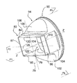
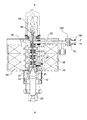
図3aおよび図3bに、本発明による遷移部の本体の2つの斜視図を示す。 Figures 3a and 3b show two perspective views of the body of the transition according to the invention.
本発明による遷移部は、縦軸ZZ’に沿った、2つの端部と、2つの端部間に通路79とを有する管形状の本体78を備える。端部の一方80は、矩形断面の管形状であり、2つの平行な長い側面84、85と、長い側面に対して垂直な2つの短い側面86、87とを有し、他方の端部90は円形の管形状である。
The transition according to the invention comprises a
矩形断面の端部80は、同様に矩形断面の適用導波管に接続するための接続フランジ(図示せず)を収容するためのものであり、円形端部90は、電子管のRF出力部に接続するためのものである。
The
遷移部の本体はさらに、矩形の管状端部80と円形の管状端部90との間の中心部分94を含む。
The transition body further includes a
遷移部の本体は、周囲媒質と接触する外面と、通路79に、管によって出力されたRF電磁波を導波管に伝播させるための内面とを備える。
The main body of the transition section includes an outer surface that comes into contact with the surrounding medium, and an inner surface for propagating the RF electromagnetic wave output by the tube in the
遷移部の本体の外面は、本体の中心部分94において、一方では、本体の端部に接続するための2つの平面的な外面100、102を備え、その面100、102は、本体78の矩形端部80の長い側面84、85に対して平行な、ZZ’軸を通る平面P1に対して対称的であるそれぞれ傾斜平面Ph、Pb内にあり、他方では、本体の前記端部に接続するための2つの他の平面的な外側接続面104、106を備え、その面104、106は、ZZ’軸を通りかつ遷移部の矩形端部の短い側面86、87に対して平行な別の平面P2の両側において対称的である。
The outer surface of the body of the transition section comprises, on the one hand, in the
2つの対称的な傾斜平面の外側接続面100、102の形状は、これらの面を通る傾斜平面Ph、Pbと本体の円形のシリンダー状端部90とが交差することにより決まる。
The shape of the outer connecting
本体の矩形端部80と中心部分94との間の接続部には、ZZ’軸に対して垂直な平面内に肩部110があり、導波管に接続するための接続フランジ(図示せず)を位置決めするためのストッパを形成している。
The connection between the
本体78の内面によって境界を定められる通路79の内部体積が、遷移部の電磁波の伝播を決定する。これらの内面は、本体の矩形端部側に、導波管の長い側面84、85に対して平行な2つの平面的な内面120、122および短い側面86、87に対して平行な2つの他の平面的な内面124、126、ならびに円形のシリンダー状端部90の側に、円錐状内側伝播面130を備える。
The internal volume of the
円錐状内面130は、本体の矩形端部80の短い側面86、87に対して平行な平面的な内面124、126と交差する2つの交差縁部140、142を有する。
The conical
本体の矩形端部の長い側面84、85に対して平行な2つの平面的な内面120、122のそれぞれを円形のシリンダー状端部90の円錐状内面130に、ZZ’軸の両側において対称的なそれぞれの曲面132、133を介して接続し、曲面132、133は、本発明の主な特徴によれば、可変長の双方向性の曲率半径を有する。
Each of the two planar
2つの傾斜平面の外側接続面100、102のZZ’軸に対する傾斜角が、図2に示す従来技術の遷移部の隅肉半径rよりも遙かに大きい隅肉半径を有する曲面132、133によって、遷移部の2つの端部の内面を接合することを可能とする。
By the
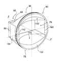
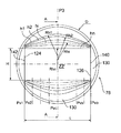
図4aに、図3aおよび図3bの遷移部の本体の円形のシリンダー状部分90の正面図を示し、接続曲面132、133を、前記曲面の水平レベルh1、h2、hi、...hn(iは1〜nの整数であり、nは水平レベルの曲線の数である)の曲線の形態で示し、図4bに、図3aおよび図3bの遷移部の本体の軸方向断面図を示す。
FIG. 4a shows a front view of the circular
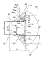
図4bに、縦軸ZZ’を通る遷移部の本体の矩形端部の長い側面84、85に対して垂直な平面P3におけるAA(図4a参照)の断面図を示す。 FIG. 4b shows a cross-sectional view of AA (see FIG. 4a) in a plane P3 perpendicular to the long side surfaces 84, 85 of the rectangular end of the transition body passing through the longitudinal axis ZZ '.
図4aによれば、接続面132、133の縁部の水平レベルh1、h2、hi、...hnの曲線のそれぞれを、それぞれ水平曲率半径Rh1、Rh2、...Rhi、...Rhnを有する湾曲部分に内接させ、前記水平曲率半径の各々は、本体の矩形端部80の短い側面86、87に対して平行な各回転軸の周りを回転する。
According to FIG. 4a, the horizontal levels h1, h2, hi,. . . Each of the hn curves is represented by a horizontal curvature radius Rh1, Rh2,. . . Rhi,. . . Inscribed in a curved portion having Rhn, each of the horizontal radii of rotation rotates about a respective axis of rotation parallel to the
水平曲率半径は、対象の水平レベルh1、h2、hi、...hnの曲線に依存して可変長であり、かつ本体の矩形セクションの短い側面86、87に対して垂直な平面において回転の中心が可変である。
The horizontal radius of curvature is the horizontal level h1, h2, hi,. . . Depending on the curve of hn, the length of rotation is variable and the center of rotation is variable in a plane perpendicular to the
これは、第1の水平曲率半径Rh1が、円錐状内面130と各曲面132、133との間の交点である水平レベルh1を決定する有限長を有するためである。最後の水平曲率半径Rhnは、曲面132、133と、今回は本体の矩形セクションの長い側面の各平面的な内面120、122との間の交点である最後の水平レベルhnを決定する有限長を有する。水平曲率Rh1、Rh2、...Rhi、...Rhnの中間半径のセット(これらの中では、位置iの中間の水平曲率半径Rhiである)は、曲面132、133の形状を決定する。
This is because the first horizontal curvature radius Rh1 has a finite length that determines the horizontal level h1 that is the intersection between the conical
図4bに、本体の矩形端部80の長い側面84、85に対して垂直な各切断平面Pv1、Pv2、..Pvx、...Pvp(xは1〜pの整数であり、pは垂直レベルの曲線の数である)における内側曲面の垂直レベルv1、v2、..vx、...vpの曲線を示す。
In FIG. 4b, each cutting plane Pv1, Pv2,... Perpendicular to the
図4bを参照すると、内側接続面の縁部における垂直レベルv1、v2、..vx、...vpの曲線の各々は、それぞれ垂直曲率半径Rv1、Rv2..、Rvx、...Rvc、...Rvpを有する湾曲部分に内接し、前記垂直曲率半径の各々は、本体の矩形端部80の長い側面84、85に対して平行な各回転軸の周りで回転する。
Referring to FIG. 4b, the vertical levels v1, v2,. . vx,. . . Each of the curves of vp has vertical curvature radii Rv1, Rv2,. . , Rvx,. . . Rvc,. . . Inscribed in the curved portion having Rvp, each of the vertical radii of rotation rotates about a respective axis of rotation parallel to the
垂直曲率半径は、対象の垂直レベルv1、v2、..vx、...vpの曲率に従って可変長であり、かつ本体の矩形セクションの短い側面に対して平行な平面Pv1、Pv2、..Pvx、...Pvpにおける回転の中心が可変である。 The vertical radius of curvature is the target vertical level v1, v2,. . vx,. . . A plane Pv1, Pv2,... that is variable length according to the curvature of vp and is parallel to the short side of the rectangular section of the body. . Pvx,. . . The center of rotation in Pvp is variable.
これは、本体のZZ’軸を通る平面P3における垂直曲率半径Rvcが、矩形セクションの短い側面の内面124、126を通る端部の長い側面に対して垂直な各平面において第1の垂直曲率半径Rv1または最後の垂直曲率半径Rvpよりも大きいためである。これらの第1の垂直曲率半径Rv1および最後の垂直曲率半径Rvp(これらの値は同じである)は、本体の矩形端部の長い側面84、85に対して平行な内面120、122に接続するための2つの内面132、133の垂直曲率半径のうち最も小さいものである。
This is because the vertical radius of curvature Rvc in the plane P3 passing through the ZZ ′ axis of the body is the first vertical radius of curvature in each plane perpendicular to the long side of the end passing through the short side
本発明による遷移部では、矩形セクションの長い側面84、85に対して垂直な平面内にある接続曲面上の2つの対称点間の距離は、矩形セクションから円形セクションに向かう間に漸次的に増大する。
In the transition according to the invention, the distance between two symmetry points on the connecting curved surface in a plane perpendicular to the
遷移部の本体の内面の形状によって、特に遷移部の中心部分において、従来技術の遷移部よりも遙かに大きい曲率を得ることが可能となる。この特徴は、遷移部の内側接続面において伝達された同じRF電力によって電界が著しく低減することによって明白になる。それにより、遷移部の絶縁破壊強度が著しく改善する。 Depending on the shape of the inner surface of the body of the transition part, it is possible to obtain a much larger curvature than the transition part of the prior art, particularly in the central part of the transition part. This feature is manifested by a significant reduction in the electric field due to the same RF power transmitted at the inner interface of the transition. Thereby, the dielectric breakdown strength of the transition portion is remarkably improved.
特に図3a、3b、4a、4bに示す遷移部の一実施形態では、遷移部の本体の寸法は、
−ZZ’軸に沿った長さL=99mm、
−円形端部90の直径D=205mm、
−円錐状内面130の円錐の頂角θ=135°、
−矩形端部80の内部矩形セクションの高さH=82mmおよび幅L=165mm、
−ZZ’軸に対する、外面の平面PhおよびPbの傾斜角度α=52°、および
−ZZ’軸に対して垂直でありかつこの軸を通る平面P3における垂直曲率半径Rvcは60mm
である。この垂直曲率半径Rvcは、図2に示す従来技術の遷移部の隅肉半径rよりも遙かに大きく、約2〜3mmである。
In particular, in one embodiment of the transition shown in FIGS. 3a, 3b, 4a, 4b, the dimensions of the body of the transition are
-Length L = 99 mm along the ZZ 'axis,
The diameter D of the
The apex angle θ of the cone of the conical
The height H = 82 mm and the width L = 165 mm of the inner rectangular section of the
The inclination angle α of the outer planes Ph and Pb with respect to the −ZZ ′ axis is α = 52 °, and the vertical curvature radius Rvc in the plane P3 that is perpendicular to and passes through this axis is 60 mm.
It is. This vertical radius of curvature Rvc is much larger than the fillet radius r of the transition portion of the prior art shown in FIG.
本発明による遷移部のこの新規のタイプの主な結論の1つは、導波管および遷移部における加圧ガスが、空気または窒素など非温室効果ガスでありかつ保守管理者に対して無害であり得ることである一方、遷移部に十分な絶縁破壊強度を得ることができることである。 One of the main conclusions of this new type of transition according to the present invention is that the pressurized gas in the waveguide and transition is a non-greenhouse gas such as air or nitrogen and is harmless to maintenance personnel. On the other hand, it is possible to obtain sufficient dielectric breakdown strength at the transition portion.
例えば、図1に示すL帯および本発明による遷移部で動作するクライストロンにより出力された5MWの供給されたRF電力の場合、2バールの空気圧下で、矩形断面部分の平面的な内面120、122、124、126における電界は約0.88kV/mmである。接続面130、132における電界は約0.94kV/mmである。これは、図2に示す従来技術の遷移部の接続隅肉部70に生じる電界レベル(1.8kV/mm)を遙かに下回る電界レベルである。
For example, for the L band shown in FIG. 1 and a 5 MW supplied RF power output by a klystron operating in the transition according to the invention, the planar
それゆえ、本発明による遷移部の可変の双方向性の半径を備える特定のプロファイルによって、この回路(遷移部+WR650導波管)において、波の形態のマイクロ波電力の通過によって生じた電界を、前記回路内部で使用する必要があるのは空気または窒素のみであるように十分に低減することが可能となる。 Therefore, with the specific profile with a variable bidirectional radius of the transition according to the invention, the electric field produced by the passage of microwave power in the form of waves in this circuit (transition + WR650 waveguide) It is possible to sufficiently reduce so that only air or nitrogen needs to be used inside the circuit.
加圧ガスとして空気を使用することの利点は、保守がより単純になり、かつ人員に対して危険がないことである。 The advantage of using air as the pressurized gas is that maintenance is simpler and there is no danger to personnel.
本発明による遷移部はまた、通過する電磁波に適合され、最適な反射係数をもたらす。 The transition according to the invention is also adapted to the electromagnetic wave passing through, resulting in an optimal reflection coefficient.
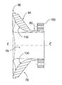
図5に、適用導波管(図示せず)に接続するためのフランジ150に固定された遷移部の本体78を含む、本発明による遷移部の代替的な形態を示す。
FIG. 5 illustrates an alternative form of transition according to the present invention including a
導波管と同じ矩形断面のフランジ150を、遷移部の本体78の矩形端部80に封止式に固定する。
A
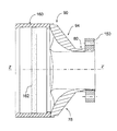
図6に、適用導波管に接続するためのフランジと、円形のシリンダー状分離窓とを含む本発明による遷移部の別の代替的な形態を示す。 FIG. 6 shows another alternative form of transition according to the present invention that includes a flange for connection to an applied waveguide and a circular cylindrical separation window.
図6に、本体78の矩形端部80に固定された、図5に示す接続フランジ150と、円形のシリンダー状分離窓160とを含む、本発明による遷移部の別の代替的な形態を示す。分離窓160は、本体78の円形部分90と同軸であり、直径が同じであり、かつそれに封止式に固定されている。
FIG. 6 shows another alternative form of transition according to the present invention including the connecting
分離窓160は、電磁波を透過するセラミック製の同軸の分離ディスク162を含み、それにより、2つの異なる物理的な媒体、一方では電子管における真空および他方では導波管における加圧ガスを分離する。
The
フランジ150および分離窓160を、例えばろう付け作業によって本体78に固定してもよい。
The
図7に、図6に示す実施形態による本発明による遷移部を含む図1のクライストロンを示す。 FIG. 7 shows the klystron of FIG. 1 including a transition according to the invention according to the embodiment shown in FIG.
図6のこの実施形態では、管のRF電力出力部を、本発明による遷移部の窓160に封止式に接続する。適用導波管もまた、その矩形端部の側で遷移部に、遷移部のフランジ150を介して封止式に固定された接続フランジ(図示せず)を含む。
In this embodiment of FIG. 6, the RF power output of the tube is sealingly connected to the
78 管形状の本体
79 通路
80 矩形端部
84、85 長い側面
86、87 短い側面
90 円形端部
94 中心部分
100、102 平面的な外側接続面
104、106 平面的な外側接続面
110 肩部
120、122 平面的な内側伝播面
124、126 平面的な内面
130 円錐状内側伝播面
132、133 接続曲面
140、142 交差縁部
150 接続フランジ
160 分離窓
P1、P2、P3 ZZ’軸を通る平面
Ph、Pb 傾斜平面
Pv1、Pvp 矩形セクションの短い側面の平面的な内面を通る、矩形端部の長い側面に対して垂直な平面
Rh1、Rh2、Rhi、Rhn 水平曲率半径
Rv1、Rv2、Rvc、Rvx、Rvp 垂直曲率半径
78
Claims (9)
前記長い側面(84、85)に対して平行な前記平面的な内側伝播面(120、122)の各々が、双方向性の曲率半径を有する各接続曲面(132、133)を介して前記円錐状内側伝播面(130)に接合していることを特徴とするマイクロ波出力遷移部。 Two ends (80, 90) along the longitudinal axis ZZ ′ and an inner surface (120, 122, 124, 126, 130, 132, 133) for propagating electromagnetic waves between the two ends are provided. A microwave power transition for a high power electron tube comprising a tube-shaped body (78) having a passage (79) having one end (90) in the form of a circular cylindrical tube being conical. The other end (80), including the inner propagation surface (130) and in the form of a rectangular cross-section tube, has two long sides (84, 85) and two short sides (86) perpendicular to the long sides. 87), and the passage is parallel to the long side surfaces (84, 85), two planar inner propagation surfaces (120, 122), and the short side surfaces (86, 87). And two other planar inner surfaces (124, 126) parallel to each other In the microwave output transition section,
Each of the planar inner propagation surfaces (120, 122) parallel to the long side surfaces (84, 85) is connected to the cone via connecting curved surfaces (132, 133) having bidirectional radii of curvature. A microwave output transition portion characterized by being joined to the inner propagation surface (130).
−前記ZZ’軸に沿った長さL=99mm、
−前記円形端部(90)の直径D=205mm、
−前記円錐状内面(130)の円錐の頂角θ=135°、
−前記矩形端部(80)の前記内部矩形セクションの高さH=82mmおよび幅L=165mm、および
−前記ZZ’軸に対して垂直でありかつこの軸を通る前記平面(P3)における垂直曲率半径Rvcは60mm
であることを特徴とする請求項1〜6のいずれか一項に記載のマイクロ波遷移部。 In one particular embodiment, the dimensions of the body (78) of the transition are:
A length L = 99 mm along the ZZ ′ axis,
The diameter D = 205 mm of the circular end (90),
The apex angle θ of the cone of the conical inner surface (130) = 135 °,
The height H = 82 mm and the width L = 165 mm of the internal rectangular section of the rectangular end (80), and the vertical curvature in the plane (P3) perpendicular to and passing through the ZZ ′ axis Radius Rvc is 60mm
The microwave transition unit according to any one of claims 1 to 6, wherein the microwave transition unit is a part.
Applications Claiming Priority (2)
| Application Number | Priority Date | Filing Date | Title |
|---|---|---|---|
| FR0807393A FR2940519A1 (en) | 2008-12-23 | 2008-12-23 | ADAPTED RF OUTPUT TRANSITION FOR ELECTRONIC POWER HYPERFREQUENCY TUBE |
| FR0807393 | 2008-12-23 |
Publications (2)
| Publication Number | Publication Date |
|---|---|
| JP2010157504A true JP2010157504A (en) | 2010-07-15 |
| JP5830816B2 JP5830816B2 (en) | 2015-12-09 |
Family
ID=41172464
Family Applications (1)
| Application Number | Title | Priority Date | Filing Date |
|---|---|---|---|
| JP2009291037A Expired - Fee Related JP5830816B2 (en) | 2008-12-23 | 2009-12-22 | RF power transition suitable for high power microwave electron tube |
Country Status (4)
| Country | Link |
|---|---|
| US (1) | US8344626B2 (en) |
| EP (1) | EP2202774B1 (en) |
| JP (1) | JP5830816B2 (en) |
| FR (1) | FR2940519A1 (en) |
Families Citing this family (1)
| Publication number | Priority date | Publication date | Assignee | Title |
|---|---|---|---|---|
| CN102569966A (en) * | 2011-12-30 | 2012-07-11 | 零八一电子集团四川华昌电子有限公司 | Ultrashort rectangular-circular transitional waveguide under long-centimeter waveband |
Citations (3)
| Publication number | Priority date | Publication date | Assignee | Title |
|---|---|---|---|---|
| JPH04105701U (en) * | 1991-02-20 | 1992-09-11 | 三菱電機株式会社 | airtight high frequency window |
| JPH0684473A (en) * | 1992-09-02 | 1994-03-25 | Toshiba Corp | Microwave tube device |
| US20080136565A1 (en) * | 2006-12-12 | 2008-06-12 | Jeffrey Paynter | Waveguide transitions and method of forming components |
Family Cites Families (7)
| Publication number | Priority date | Publication date | Assignee | Title |
|---|---|---|---|---|
| CA823797A (en) * | 1969-09-23 | Telefunken Patentverwertungsgesellschaft M.B.H. | Waveguide transition member | |
| GB743801A (en) * | 1953-05-15 | 1956-01-25 | Elliott Brothers London Ltd | Improvements in or relating to waveguide mode transformers |
| GB1280842A (en) * | 1968-08-21 | 1972-07-05 | Rca Corp | Polarization rotator |
| US3818383A (en) * | 1973-02-27 | 1974-06-18 | Andrew Corp | Elliptical-to-rectangular waveguide transition |
| US5461283A (en) * | 1993-07-29 | 1995-10-24 | Litton Systems, Inc. | Magnetron output transition apparatus having a circular to rectangular waveguide adapter |
| EP1223636A1 (en) * | 2000-12-19 | 2002-07-17 | Spinner GmbH Elektrotechnische Fabrik | Overmoded hollow waveguide transition and its manufacturing method |
| US6636127B2 (en) * | 2002-02-23 | 2003-10-21 | Lockheed Martin Corp. | Broadband turnstile waveguide junction |
-
2008
- 2008-12-23 FR FR0807393A patent/FR2940519A1/en not_active Withdrawn
-
2009
- 2009-12-08 EP EP09178423.1A patent/EP2202774B1/en active Active
- 2009-12-16 US US12/639,595 patent/US8344626B2/en active Active
- 2009-12-22 JP JP2009291037A patent/JP5830816B2/en not_active Expired - Fee Related
Patent Citations (3)
| Publication number | Priority date | Publication date | Assignee | Title |
|---|---|---|---|---|
| JPH04105701U (en) * | 1991-02-20 | 1992-09-11 | 三菱電機株式会社 | airtight high frequency window |
| JPH0684473A (en) * | 1992-09-02 | 1994-03-25 | Toshiba Corp | Microwave tube device |
| US20080136565A1 (en) * | 2006-12-12 | 2008-06-12 | Jeffrey Paynter | Waveguide transitions and method of forming components |
Also Published As
| Publication number | Publication date |
|---|---|
| EP2202774A1 (en) | 2010-06-30 |
| US8344626B2 (en) | 2013-01-01 |
| US20100295636A1 (en) | 2010-11-25 |
| FR2940519A1 (en) | 2010-06-25 |
| JP5830816B2 (en) | 2015-12-09 |
| EP2202774B1 (en) | 2013-06-05 |
Similar Documents
| Publication | Publication Date | Title |
|---|---|---|
| Haworth et al. | Significant pulse-lengthening in a multigigawatt magnetically insulated transmission line oscillator | |
| US8179045B2 (en) | Slow wave structure having offset projections comprised of a metal-dielectric composite stack | |
| CN112885681B (en) | Relativistic magnetron with double-end emission cathode structure | |
| KR20180059579A (en) | Electron-coupled transformer | |
| JP5830816B2 (en) | RF power transition suitable for high power microwave electron tube | |
| US3110000A (en) | Waveguide window structure having three resonant sections giving broadband transmission with means to fluid cool center section | |
| US2966610A (en) | Electron beam tube | |
| US3205398A (en) | Long-slot coupled wave propagating circuit | |
| US3324427A (en) | Electromagnetic wave permeable window | |
| US2788464A (en) | Traveling wave electron discharge devices | |
| US3339102A (en) | High frequency electron discharge devices and wave permeable windows | |
| Shemyakin et al. | Design of MEBT for the Project X Injector Experiment at Fermilab | |
| CN220021036U (en) | A radial electron injection staggered gate structure traveling wave amplifier | |
| JPH04215233A (en) | Multibeam microwave tube provided with coaxial output | |
| RU2364977C1 (en) | O-type superhigh frequency device | |
| Rzesnicki et al. | Parasitic-modes free, high-performance operation of the European 1 MW, 170 GHz Short-Pulse Prototype Gyrotron for ITER | |
| US3433999A (en) | Non-resonant stub supports for slow wave circuits | |
| RU2747579C2 (en) | Powerful broadband klystron | |
| US3771010A (en) | Liquid cooled band edge oscillation prevention for a twt | |
| US3480828A (en) | Thyratron waveguide switch with density enhancement for operation in 27 to 40 ghz. range | |
| JP4533588B2 (en) | Klystron equipment | |
| RU2494490C2 (en) | Travelling wave tube | |
| JP5016904B2 (en) | Multi-beam klystron | |
| Pasour et al. | High‐Power, Annular‐Beam Klystron Amplifiers | |
| US3532925A (en) | Broadband waveguide transition for a centipede slow wave circuit and tubes using same |
Legal Events
| Date | Code | Title | Description |
|---|---|---|---|
| A621 | Written request for application examination |
Free format text: JAPANESE INTERMEDIATE CODE: A621 Effective date: 20121130 |
|
| A521 | Request for written amendment filed |
Free format text: JAPANESE INTERMEDIATE CODE: A523 Effective date: 20130221 |
|
| A977 | Report on retrieval |
Free format text: JAPANESE INTERMEDIATE CODE: A971007 Effective date: 20131205 |
|
| A131 | Notification of reasons for refusal |
Free format text: JAPANESE INTERMEDIATE CODE: A131 Effective date: 20131217 |
|
| A601 | Written request for extension of time |
Free format text: JAPANESE INTERMEDIATE CODE: A601 Effective date: 20140317 |
|
| A601 | Written request for extension of time |
Free format text: JAPANESE INTERMEDIATE CODE: A601 Effective date: 20140417 |
|
| A601 | Written request for extension of time |
Free format text: JAPANESE INTERMEDIATE CODE: A601 Effective date: 20140515 |
|
| A521 | Request for written amendment filed |
Free format text: JAPANESE INTERMEDIATE CODE: A523 Effective date: 20140508 |
|
| A602 | Written permission of extension of time |
Free format text: JAPANESE INTERMEDIATE CODE: A602 Effective date: 20140404 |
|
| A521 | Request for written amendment filed |
Free format text: JAPANESE INTERMEDIATE CODE: A523 Effective date: 20140616 |
|
| A521 | Request for written amendment filed |
Free format text: JAPANESE INTERMEDIATE CODE: A523 Effective date: 20140612 |
|
| A602 | Written permission of extension of time |
Free format text: JAPANESE INTERMEDIATE CODE: A602 Effective date: 20140507 |
|
| A521 | Request for written amendment filed |
Free format text: JAPANESE INTERMEDIATE CODE: A523 Effective date: 20140710 |
|
| A602 | Written permission of extension of time |
Free format text: JAPANESE INTERMEDIATE CODE: A602 Effective date: 20140605 |
|
| A131 | Notification of reasons for refusal |
Free format text: JAPANESE INTERMEDIATE CODE: A131 Effective date: 20141216 |
|
| A601 | Written request for extension of time |
Free format text: JAPANESE INTERMEDIATE CODE: A601 Effective date: 20150316 |
|
| A601 | Written request for extension of time |
Free format text: JAPANESE INTERMEDIATE CODE: A601 Effective date: 20150414 |
|
| A601 | Written request for extension of time |
Free format text: JAPANESE INTERMEDIATE CODE: A601 Effective date: 20150514 |
|
| A521 | Request for written amendment filed |
Free format text: JAPANESE INTERMEDIATE CODE: A523 Effective date: 20150615 |
|
| A521 | Request for written amendment filed |
Free format text: JAPANESE INTERMEDIATE CODE: A523 Effective date: 20150625 |
|
| TRDD | Decision of grant or rejection written | ||
| A01 | Written decision to grant a patent or to grant a registration (utility model) |
Free format text: JAPANESE INTERMEDIATE CODE: A01 Effective date: 20150804 |
|
| A61 | First payment of annual fees (during grant procedure) |
Free format text: JAPANESE INTERMEDIATE CODE: A61 Effective date: 20150806 |
|
| A521 | Request for written amendment filed |
Free format text: JAPANESE INTERMEDIATE CODE: A523 Effective date: 20150730 |
|
| A61 | First payment of annual fees (during grant procedure) |
Free format text: JAPANESE INTERMEDIATE CODE: A61 Effective date: 20151008 |
|
| R150 | Certificate of patent or registration of utility model |
Ref document number: 5830816 Country of ref document: JP Free format text: JAPANESE INTERMEDIATE CODE: R150 |
|
| R250 | Receipt of annual fees |
Free format text: JAPANESE INTERMEDIATE CODE: R250 |
|
| R250 | Receipt of annual fees |
Free format text: JAPANESE INTERMEDIATE CODE: R250 |
|
| R250 | Receipt of annual fees |
Free format text: JAPANESE INTERMEDIATE CODE: R250 |
|
| R250 | Receipt of annual fees |
Free format text: JAPANESE INTERMEDIATE CODE: R250 |
|
| R250 | Receipt of annual fees |
Free format text: JAPANESE INTERMEDIATE CODE: R250 |
|
| LAPS | Cancellation because of no payment of annual fees |