JP2010146474A - Semiconductor device - Google Patents
Semiconductor device Download PDFInfo
- Publication number
- JP2010146474A JP2010146474A JP2008325702A JP2008325702A JP2010146474A JP 2010146474 A JP2010146474 A JP 2010146474A JP 2008325702 A JP2008325702 A JP 2008325702A JP 2008325702 A JP2008325702 A JP 2008325702A JP 2010146474 A JP2010146474 A JP 2010146474A
- Authority
- JP
- Japan
- Prior art keywords
- arithmetic processing
- storage
- voltage
- period
- storage device
- Prior art date
- Legal status (The legal status is an assumption and is not a legal conclusion. Google has not performed a legal analysis and makes no representation as to the accuracy of the status listed.)
- Granted
Links
Images


Classifications
-
- Y—GENERAL TAGGING OF NEW TECHNOLOGICAL DEVELOPMENTS; GENERAL TAGGING OF CROSS-SECTIONAL TECHNOLOGIES SPANNING OVER SEVERAL SECTIONS OF THE IPC; TECHNICAL SUBJECTS COVERED BY FORMER USPC CROSS-REFERENCE ART COLLECTIONS [XRACs] AND DIGESTS
- Y02—TECHNOLOGIES OR APPLICATIONS FOR MITIGATION OR ADAPTATION AGAINST CLIMATE CHANGE
- Y02D—CLIMATE CHANGE MITIGATION TECHNOLOGIES IN INFORMATION AND COMMUNICATION TECHNOLOGIES [ICT], I.E. INFORMATION AND COMMUNICATION TECHNOLOGIES AIMING AT THE REDUCTION OF THEIR OWN ENERGY USE
- Y02D10/00—Energy efficient computing, e.g. low power processors, power management or thermal management
Abstract
Description
本発明は、半導体装置に係り、特に、低電力プロセッサ用回路技術に関する。 The present invention relates to a semiconductor device, and more particularly to a circuit technology for a low power processor.
従来、特開2000-214967号公報(特許文献1)に開示されているように、プロセッサに入力する電力制御命令信号をデコードして、装置内の回路ブロックの周波数やリーク電流を制御する方法が知られている。また、特開2004-318502号公報(特許文献2)に開示されているように、プロセッサに入力するメモリアクセス命令を検出して回路ブロックの周波数やしきい値電圧を制御する方法が知られている。更には、特開2002-229690号公報(特許文献3)に開示されているように、プロセッサ自身が他の命令から電力制御命令を発生し、装置内の回路ブロックの周波数やリーク電流を制御する方法が知られている。
リーク電流やしきい値電圧を制御する手段としては、1996年、IEEE, Journal of Solid-State Circuits, VOL.31, No.11、1770頁〜1779(非特許文献1)の"A 0.9-V, 150-MHz, 10-mW, 4 mm2, 2-D Discrete Cosine Transform Core Processor with Variable Threshold-Voltage (VT) Scheme"に記載のように、CMOSトランジスタの基板(ウエル)に電圧を印加し(この文献のFig.2を参照)、することが知られている。また、2005 年、IEEE International Electron Device Meeting Technical Digest Papers pp. 631-634(非特許文献2)や、特開2007-042730号公報(特許文献4)に開示されるように完全空乏(FD)型のSOI構造におけるCMOSトランジスタにおいて、その埋め込み酸化膜(BOX)層が30nm以下と薄いことを特徴としたトランジスタを用い、これにより、このBOX層をゲート絶縁膜と見立てたバックゲートを駆動してしきい値電圧を制御する手段が知られている。また、特開2004-318502にも開示されているように、電源と回路ブロックの間に別のMOSトランジスタを挿入する方法も知られている。
Conventionally, as disclosed in Japanese Patent Application Laid-Open No. 2000-214967 (Patent Document 1), there is a method for controlling the frequency and leakage current of a circuit block in a device by decoding a power control command signal input to a processor. Are known. Further, as disclosed in Japanese Patent Application Laid-Open No. 2004-318502 (Patent Document 2), a method of detecting a memory access instruction input to a processor and controlling the frequency and threshold voltage of a circuit block is known. Yes. Further, as disclosed in Japanese Patent Laid-Open No. 2002-229690 (Patent Document 3), the processor itself generates a power control command from another command, and controls the frequency and leakage current of the circuit block in the apparatus. The method is known.
As a means for controlling leakage current and threshold voltage, 1996, IEEE, Journal of Solid-State Circuits, VOL.31, No.11, pp. 1770-1779 (Non-Patent Document 1) "A 0.9-V , 150-MHz, 10-mW, 4 mm2, 2-D Discrete Cosine Transform Core Processor with Variable Threshold-Voltage (VT) Scheme " (See Fig. 2 in the literature). Also, in 2005, as fully disclosed in IEEE International Electron Device Meeting Technical Digest Papers pp. 631-634 (Non-patent Document 2) and Japanese Patent Laid-Open No. 2007-042730 (Patent Document 4), the full depletion (FD) type is used. In the CMOS transistor of the SOI structure, a transistor characterized in that the buried oxide film (BOX) layer is as thin as 30 nm or less is used, thereby driving the back gate assuming that the BOX layer is a gate insulating film. Means for controlling the threshold voltage are known. Further, as disclosed in Japanese Patent Laid-Open No. 2004-318502, a method of inserting another MOS transistor between a power supply and a circuit block is also known.
しかしながら、電力制御命令信号をデコードして回路ブロックの周波数やしきい値電圧を制御する方法は種々あり、それらが一様に電力削減に効果があるわけではない。特に、近年の半導体装置では、そのメモリシステムは一般に階層構造を持ち、これをいかに制御するかが高性能や低電力実現の鍵となって来ている。また、半導体装置自体も大型化、複雑化しており、一般には複数のプロセッサ(演算ブロック)を多数個用いて並列動作を行わせ、またネットワークで接続して、高性能や低電力実現の鍵となって来ている。この中で、電力制御命令信号をデコードして回路ブロックの周波数やしきい値電圧を制御する時にメモリに階層構造が有る時に、このメモリへのアクセス形態に応じた半導体装置の回路ブロックの周波数やしきい値電圧の制御する効果的な方法についての従来の検討は無かった。 However, there are various methods for decoding the power control command signal to control the frequency and threshold voltage of the circuit block, and they are not effective in reducing power uniformly. In particular, in recent semiconductor devices, the memory system generally has a hierarchical structure, and how to control the memory system is the key to realizing high performance and low power. In addition, the size and complexity of semiconductor devices themselves are generally increasing.In general, multiple processors (computing blocks) are used for parallel operation and connected via a network, which is the key to realizing high performance and low power. It is becoming. Among these, when the memory control has a hierarchical structure when the power control command signal is decoded to control the frequency and threshold voltage of the circuit block, the frequency of the circuit block of the semiconductor device corresponding to the access form to the memory There has been no conventional study on an effective method of controlling the threshold voltage.
そこで、本発明の目的は、回路性能を落さずに回路の消費電力を削減するための効率的な方法を提供することにある。 Accordingly, an object of the present invention is to provide an efficient method for reducing power consumption of a circuit without degrading circuit performance.
上記目的を達成するための代表的な手段を以下に示す。第1の手段としては、メモリが階層構造となっているシステムにおいて、キャッシュミスが生じた後、メインメモリの先頭アドレスを検出する命令を検出して演算器を第1の低電力モードに切り替えるものである。また、先頭アドレスが見つかった情報がメモリより発信されたら演算器を元の高速モードに切り替えるものである。第2の手段としては、先頭アドレスが見つかった後、メモリより演算器が備えるキャッシュメモリへの格納と平行して行われる演算器の動作を第2の低電力モードに切り替えて行うものである。 Representative means for achieving the above object will be described below. As a first means, in a system in which the memory has a hierarchical structure, after a cache miss occurs, an instruction for detecting the head address of the main memory is detected and the arithmetic unit is switched to the first low power mode. It is. Further, when the information where the head address is found is transmitted from the memory, the arithmetic unit is switched to the original high speed mode. As a second means, after the head address is found, the operation of the arithmetic unit performed in parallel with the storage in the cache memory provided in the arithmetic unit from the memory is switched to the second low power mode.
メモリが階層構造となっているシステムにおいて、キャッシュミスが生じた後、メインメモリの先頭アドレスを検出する動作は、高速な大型システムでも100ナノ秒からマイクロ秒のオーダーでの時間を要する。この間は、演算器の特定の部分のみ動いておればよく、演算器の多くの部分は停止することができ、また、演算器を構成しているMOSトランジスタのしきい値電圧を絶対値で大きくしてリーク電流を低減することができる。
上記のみでも効果は大きいが、メモリより演算器が備えるキャッシュメモリへの格納の転送速度は一般に演算器がキャッシュメモリを用いて行う演算速度よりも一桁以上遅い。よって、第2の手段により、この期間に演算器が第2の低電力モードである低速かつしきい値電圧がキャッシュメモリを用いて行う時よりも高い値とできることにより、本来の全体の動作性能は落さずに、低電力化が可能となるのである。
In a system in which the memory has a hierarchical structure, the operation of detecting the start address of the main memory after a cache miss occurs requires time on the order of 100 nanoseconds to microseconds even in a high-speed large system. During this time, only a specific part of the computing unit needs to be moved, many parts of the computing unit can be stopped, and the threshold voltage of the MOS transistor constituting the computing unit is increased in absolute value. Thus, the leakage current can be reduced.
Even if only the above is effective, the transfer speed of storage to the cache memory included in the arithmetic unit is lower than that of the memory by one digit or more than the arithmetic speed performed by the arithmetic unit using the cache memory. Therefore, the second means allows the arithmetic unit to operate at the low speed and the threshold voltage in the second low power mode during this period and to have a higher value than when the cache memory is used. Therefore, it is possible to reduce the power without dropping.
メモリが階層構造となっているシステムにおいて、キャッシュミスが生じた後、メインメモリの先頭アドレスを検出する動作の間は、演算器を構成しているMOSトランジスタのしきい値電圧を絶対値で大きくしてリーク電流を低減し、これにより回路性能を落さずに回路の消費電力を削減することができる。 In a system with a hierarchical memory structure, the threshold voltage of the MOS transistor constituting the arithmetic unit is increased in absolute value during the operation of detecting the start address of the main memory after a cache miss occurs. Thus, the leakage current can be reduced, thereby reducing the power consumption of the circuit without degrading the circuit performance.
本発明の第1の実施例を図1を用いて説明する。この実施例の主要な内容は、半導体チップCHIP上のメモリコントローラがメモリ(主記憶)の制御を行うが、このメモリコントローラの動作状態に応じた、又は動作状態を示す信号によって、これがメモリ(主記憶)の先頭アドレスを探す状態となっている期間、演算を行う回路ブロックPUの電力状態を変化させるものである。全体の構成例は、半導体チップCHIP上に少なくともひとつの演算を行う回路ブロックPUがあり、これは電力状態を変化できる機能を備えており、内部バスBUS1にキャッシュメモリCMと共に接続されており、このBUS1にCHIP上の色々な回路ブロックを統括管理するCPUと、メモリと、外部との信号のやり取りを行なう回路ブロックでありがIO接続されている。IOはチップの外へのバスBUS3は接続され、このBUS3には例えばファイルメモリが接続されている。ファイルメモリは例えばフラッシュメモリやHDDなどで構成される。BUS1にはメモリコントローラが接続され、このメモリコントローラには、チップの外へのバスBUS2が接続され、BUS2にはメモリ(主記憶)が接続される。このメモリ(主記憶)は、例えばDRAMやMRAMなどの磁性体メモリなどである。このような構成において、前述のPUの回路CKTはCMOS素子で構成されており、電源は高電位Vdは、低電位はVsであるが、その基板又はバックゲートの電圧を制御できるようになっている。この基板又はバックゲートに与える電圧及びその端子がVP及びVNであり、pMOS用がVPであり、nMOSがVNである。これらの値は制御する回路ブロックがBBコントローラであり、回路CKTに与えるクロックCLKの周波数を制御する回路ブロックがCLKGである。これらは、PUひとつ毎に準備される場合もあれば、動作内容に応じて複数のPUで纏められることもある。
A first embodiment of the present invention will be described with reference to FIG. The main contents of this embodiment are that the memory controller on the semiconductor chip CHIP controls the memory (main memory). This is controlled by a signal corresponding to or indicating the operation state of the memory controller. The power state of the circuit block PU that performs the operation is changed during the period in which the head address of the memory is searched. The entire configuration example includes a circuit block PU that performs at least one operation on the semiconductor chip CHIP, which has a function of changing the power state, and is connected to the internal bus BUS1 together with the cache memory CM. The
また、共通部分を取り出して、これ以外を各PUに備える場合もある。これらBBコントローラとCLKGによって、PUの電力状態を変えることができる。この電力状態を変える信号が、MSKとMSBであり、共にメモリコントローラの状態による信号である。つまり、メモリコントローラがメモリ(主記憶)の先頭アドレスを探す状態になっていることを示す信号であり、この信号によって、PUの回路CKTの周波数及び基板電圧(バックゲート電圧)が変えられ、低電力な状態とすることができるのである。なお、このメモリコントローラの状態は、BUS1に接続されたCPUが行っているので、このMSKとMSBはCPUが発生した信号であると言うこともできる。このような構成により、本発明では演算を行う回路ブロックPUがキャッシュメモリCMの情報のみでは動作が行えず(キャッシュミス)、CHIP外部のメモリ(主記憶)の先頭アドレスを探しに行っている期間において、MSKとMSBによって回路CKTの周波数と基板又はバックゲートに与える電圧を変えて、回路ブロックPUを低電力な状態を取ることができるという特徴がある。なお、回路ブロックPUは複数個存在する場合は、そのそれぞれにおいてこのような低電力な状態を取ることができるという特徴がある。 Moreover, a common part may be taken out and other PUs may be provided in each PU. The power state of the PU can be changed by these BB controller and CLKG. The signals for changing the power state are MSK and MSB, both of which are signals depending on the state of the memory controller. In other words, this signal indicates that the memory controller is in a state of searching for the start address of the memory (main memory). By this signal, the frequency of the circuit CKT of the PU and the substrate voltage (back gate voltage) are changed, and the signal is low. It can be in a power state. Note that since the state of the memory controller is performed by the CPU connected to BUS1, it can be said that the MSK and MSB are signals generated by the CPU. With such a configuration, in the present invention, the circuit block PU that performs the operation cannot operate with only the information in the cache memory CM (cache miss), and is in the period of searching for the start address of the memory outside the CHIP (main memory) The circuit block PU can be in a low power state by changing the frequency of the circuit CKT and the voltage applied to the substrate or the back gate by MSK and MSB. It should be noted that when there are a plurality of circuit blocks PU, each of them has a feature that it can take such a low power state.
図2は、本発明の動作の主要な部分例を示したものである。MSBとMSKは、図1の回路CKTに与えるクロック周波数と基板電圧(バックゲート電圧)を変化させる信号である。VPとVNはその基板電圧(バックゲート電圧)信号であり、CLKはそのクロック周波数である。図1で、キャッシュメモリへのミスが生じ、メモリ(主記憶)の先頭アドレスを探す状態に時刻t1においてなったとしよう。すると、MSBとMSKが切り替わり、より電力の小さな状態へ回路CKTは移行する。すなわち、VPはそれまので電位VPLからVPHへ、VNはそれまのでVNLからVNHへ変化する。ここで回路CKTにおいては、VPLとVNLの電位では、pMOSもnMOSもそのしきい値電圧は低く高速動作が可能である。一方、VPHとVNHの電位では、pMOSとnMOSのしきい値電圧は高くリーク電流を低く抑えることができる。このt1では、CLKも変化させる。時刻t1以前では、高い周波数f1であったが、ここで低い周波数f2に切り替わる。これによって、メモリ(主記憶)の先頭アドレスを探す状態では、周波数は低く、しきい電圧は高いので、充放電電力もリーク電力も低く抑えることができる。この後、メモリ(主記憶)の先頭アドレスを探す動作が終了すると、この時刻t2で再びMSBとMSKが切り替わり、VPとVNはそれぞれVPLとVNLに戻り、CLKはf1に戻る。これにより高速動作が可能な状態となる。このように本実施例では、メモリ(主記憶)の先頭アドレスを探す状態において、電力を低く抑えることが可能となるのである。なお、後述するが、t2において、メモリ(主記憶)からのデータを用いて直接PUが動作を行う場合があり、これは一般的にキャッシュメモリCMの内容で動作を行う時よりも低速である。このため、これに適したクロック周波数CLKと基板電圧(バックゲート電圧) VPとVNを与えることもできる。 FIG. 2 shows an example of a main part of the operation of the present invention. MSB and MSK are signals for changing the clock frequency and the substrate voltage (back gate voltage) applied to the circuit CKT in FIG. VP and VN are the substrate voltage (back gate voltage) signals, and CLK is the clock frequency. In FIG. 1, it is assumed that a cache memory error occurs and the state of searching for the start address of the memory (main memory) is reached at time t1. Then, MSB and MSK are switched, and the circuit CKT shifts to a state where power is smaller. That is, VP changes from potential VPL to VPH, and VN changes from VNL to VNH. Here, in the circuit CKT, at the potentials VPL and VNL, the threshold voltages of both the pMOS and the nMOS are low and high speed operation is possible. On the other hand, at the potentials VPH and VNH, the threshold voltages of the pMOS and nMOS are high and the leakage current can be kept low. At t1, CLK is also changed. Before the time t1, the frequency f1 was high, but here it switches to the low frequency f2. As a result, in the state where the head address of the memory (main memory) is searched, the frequency is low and the threshold voltage is high, so that the charge / discharge power and the leak power can be kept low. Thereafter, when the operation for searching for the head address of the memory (main memory) is completed, the MSB and MSK are switched again at this time t2, VP and VN return to VPL and VNL, respectively, and CLK returns to f1. As a result, high-speed operation is possible. As described above, in this embodiment, it is possible to keep the power low in a state where the head address of the memory (main memory) is searched. As will be described later, at t2, the PU may directly operate using data from the memory (main memory), which is generally slower than when operating on the contents of the cache memory CM. . Therefore, the clock frequency CLK and the substrate voltages (back gate voltages) VP and VN suitable for this can be given.
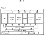
ここで本発明が適用される半導体装置のメモリの階層構造を図3に示す。
プロセッサに対してレジスタ−キャッシュ−主記憶−ファイル記憶と構成され、一般にプロセッサに近いほど、スピードは速いが容量は小さい。プロセッサは、図1の演算を行う回路ブロックPUやCPUであり、図1では省略しているが実行中又は次に実行する命令やデータを蓄えておくレジスタを有している。この下にはキャッシュがあり、図1のキャッシュメモリCMなどでありプロセッサが当面の演算を行うのに必要なデータを蓄えておく。このキャッシュはプロセッサの動作速度と同じか近い周波数(1/2や1/4)と高速に動作する。主記憶は、このキャッシュに入りきれない情報を蓄えておくものであり、キャッシュよりも低速であるが大きな記憶容量を備えている。このメモリとキャッシュメモリとのデータのやり取りは、纏まった大きさの単位で行われる。この動作は、先頭のアドレスをアクセスする動作と纏まった単位のデータを連続的に主記憶よりキャッシュへ転送する動作の2つとからなる。このうち、後者の転送する動作はプロセッサの周波数の一桁低い周波数程度であるが、前者の先頭のアドレスをアクセスする動作はこれよりも低速である。これは、バスの衝突を避けるためにプロセッサと主記憶が記憶内容を特定したことを確認する動作や、主記憶を構成するメモリのアクセス時間の制約などによる。これを制御しているのがメモリコントローラである。本発明は、先頭のアドレスをアクセスする動作が半導体装置では起こることを利用し、その間のプロセッサを低速動作又は停止させ、MOSトランジスタのしきい値電圧も高くしてリーク電力を抑え、低電力化を図るものである。この先頭のアドレスをアクセスする動作は通常の動作で起こるため、本発明によって処理性能が低くなることはない。メモリの階層構造としては、更にファイル記憶がある。これは、HDDやフラッシュメモリで構成された巨大な容量のメモリであるが、一般的に速度は遅い。よって、一般的な計算では、これに必要な情報は一旦主記憶に取り込んでから行う。又は、動作中であれば、不要な情報内容となった主記憶の部分に予測してファイル記憶内容を転送するなどこの動作が見えないようにする工夫をする。ファイル記憶にアクセスしている時間は長いため、このときはプロセッサを止めてしまうことは行われてきた。本発明は、主記憶の動作を解析した結果、ここに動作速度を損なわずに電力を削減できる状態を見出し、考案したものである。
FIG. 3 shows a hierarchical structure of a memory of a semiconductor device to which the present invention is applied.
The processor is configured as register-cache-main memory-file storage. Generally, the closer to the processor, the faster the speed but the smaller the capacity. The processor is a circuit block PU or CPU that performs the operation of FIG. 1, and has a register that stores an instruction or data to be executed or to be executed next, which is omitted in FIG. Below this is a cache, such as the cache memory CM shown in FIG. 1, which stores data necessary for the processor to perform the current operation. This cache operates at a high speed with a frequency (1/2 or 1/4) the same as or close to the operating speed of the processor. The main memory stores information that cannot be stored in the cache, and has a large storage capacity although it is slower than the cache. Data exchange between the memory and the cache memory is performed in units of a group size. This operation consists of two operations: an operation of accessing the head address and an operation of transferring a unit of data continuously from the main memory to the cache. Among these, the latter transfer operation is about one digit lower than the frequency of the processor, but the operation of accessing the former head address is slower than this. This is due to, for example, an operation for confirming that the processor and the main memory have specified the stored contents in order to avoid a bus collision, and a restriction on the access time of the memory constituting the main memory. This is controlled by a memory controller. The present invention utilizes the fact that the operation of accessing the head address occurs in the semiconductor device, and operates or stops the processor during that time, and also increases the threshold voltage of the MOS transistor to suppress the leakage power, thereby reducing the power consumption. Is intended. Since the operation of accessing the head address occurs in a normal operation, the processing performance is not lowered by the present invention. As a hierarchical structure of the memory, there is a file storage. This is a huge-capacity memory composed of an HDD or a flash memory, but is generally slow. Therefore, in general calculation, information necessary for this is once taken into the main memory. Or, if it is in operation, a measure is taken to prevent this operation from being seen, such as predicting the portion of the main memory that has become unnecessary information content and transferring the file storage content. Since it takes a long time to access the file store, it has been attempted to shut down the processor at this time. As a result of analyzing the operation of the main memory, the present invention has found and devised a state where power can be reduced without impairing the operation speed.
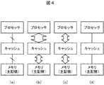
図4に、レジスタは省力したが、計算中のプロセッサとキャッシュとメモリ(主記憶)のデータのやり取りの大きさに注目した関係を示す。ファイル記憶は、主に計算は終了後、又は計算準備のためのデータをやり取りに使用するので省略してある。(a)は、階層構造を示した図であり、プロセッサに対して、キャッシュとメモリ(主記憶) とがあり、一般にキャッシュは高速だがその容量は小さく、メモリ(主記憶) は中速(〜低速)であるがその容量は大きい。一般には、キャッシュメモリはプロセッサと同じチップ上のSRAMが用いられるが、最近容量がそれでも大きなものが要求されるようになってきており、DRAMが用いられる場合もある。また、磁性体メモリもその無限回の書き換え回数のために使用されることもある。この時は、磁性体メモリは不揮発のためこれを活かした使い方も可能である。メモリ(主記憶) は、主にはDRAMであるが、これも磁性体メモリが使用される場合がある。このような構成において、(b)〜(d)の3つの動作モードが存在する。(b)は、プロセッサがキャッシュの記憶内容を用いて高速に動作している場合であり、プロセッサの最高性能を引き出すことができる。(c)は、主記憶中のデータを直接用いてプロセッサが動作している状態であり、データの転送速度によって速度は制限されてしまう。一般にはプロセッサの最高性能の一桁低い性能となってしまう転送速度となる。(d)は、これまでも説明してきた、先頭アドレスを探しに行っている状態であり、プロセッサそのものは演算を行っていない。本発明を用いて、プロセッサを低電力な状態にできるのは第1には(d)の期間であるが、(c)の期間もプロセッサの動作は最高性能の一桁低い動作しかできないため、本発明を用いてしきい値電圧も高くしてリーク電力を下げることができる。 FIG. 4 shows a relationship where attention is paid to the size of data exchange between the processor, the cache, and the memory (main memory) while the registers are labor-saving. The file storage is omitted because the calculation is mainly completed or data for calculation preparation is used for the exchange. (A) is a diagram showing a hierarchical structure. For a processor, there are a cache and a memory (main memory). Generally, the cache is high speed but its capacity is small, and the memory (main memory) is medium speed (~ Low speed) but its capacity is large. In general, an SRAM on the same chip as the processor is used as the cache memory, but recently, a memory having a large capacity has been required, and a DRAM may be used. Also, a magnetic memory may be used for the infinite number of rewrites. At this time, since the magnetic memory is non-volatile, it can be used by utilizing it. The memory (main memory) is mainly a DRAM, but a magnetic memory may also be used. In such a configuration, there are three operation modes (b) to (d). (b) is a case where the processor is operating at high speed using the stored contents of the cache, and the maximum performance of the processor can be derived. (C) is a state in which the processor is operating directly using data stored in the main memory, and the speed is limited by the data transfer speed. In general, the transfer speed is one order of magnitude lower than the maximum performance of the processor. (D) is the state which has been described so far to search for the head address, and the processor itself is not performing an operation. Using the present invention, the processor can be put into a low power state in the period (d) in the first place, but since the operation of the processor can only be an order of magnitude lower than the maximum performance in the period (c), By using the present invention, the threshold voltage can be increased and the leakage power can be reduced.
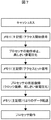
図5は、この(b)〜(d)の3つの動作モードの時間配分を示した例である。(1)は、プロセッサの最高性能を引き出せるプログラムの例であり、分子動力学の第1原理計算の例である。この例では、56%の期間が(b)のモードであり、(c)が25%、(d)が19%である。この例では、本発明を用いて、プロセッサを低電力な状態にできるのは、先頭アドレスを探しに行っている期間では19%の部分である。(2)は、(1)のようにキャッシュの内容のみでの計算が占める割合が大きくない例であり、多くのプログラムはこのような傾向となってしまう。この例では、20%は(b)のモードとできた例であり、45%が(c)であり、35%が(d)である。この例では、先頭アドレスを探しに行っている期間のみに着目した場合でも35%の期間をプロセッサの電力が小さな状態とできる。 FIG. 5 is an example showing time distribution in the three operation modes (b) to (d). (1) is an example of a program that can bring out the maximum performance of the processor, and is an example of the first principle calculation of molecular dynamics. In this example, the period of 56% is the mode (b), (c) is 25%, and (d) is 19%. In this example, the processor can be put into a low power state using the present invention in a portion of 19% during the period of searching for the head address. (2) is an example in which the ratio of calculation only by the contents of the cache is not large as in (1), and many programs tend to have such a tendency. In this example, 20% is an example in which the mode (b) can be achieved, 45% is (c), and 35% is (d). In this example, even when attention is paid only to the period in which the head address is searched for, the power of the processor can be kept low for a period of 35%.
ここで、基板電圧(バックゲート電圧)及びクロック周波数を変える回路ブロック図を図6に示しておく。回路CKTは、本発明を構成するしきい値電圧とクロック周波数が制御可能なCMOS回路であり、その電源電圧はVdとVsであり、基板電圧(バックゲート電圧)の端子及びその電圧はVP及びVNであり、入力しているクロックの端子及びその周波数はCLKである。VP及びVNをメモリへのアクセス状況に応じて変化させるBBコントローラは、プロセス変動などに応じた電圧を発生するVthp及びVthnを備えている。それぞれ電源VddとVssで動作し(これはVdとVsと同一の場合もあれば、異なる場合もある)、VthpではpMOSと抵抗とで電圧が発生させられ、VthnではnMOSと抵抗とで電圧を発生する。これらの電圧は、使用したpMOS及びnMOSがプロセス条件を反映することによって、プロセス条件に応じた電圧を発生する。これによってプロセスの変動を基板電圧(バックゲート電圧)の電圧によって補償することが可能となる。これらの電圧は、一旦OPアンプで安定化される。このときにはプロセスによらない基準電圧Vref.が必要である。これは良く知られたバンドギャップジェネレータなどで発生できる。この出力電圧が、それぞれVPL及びVNLであり、本発明では回路CKTの高速動作に適したしきい値となる基板電圧(バックゲート電圧)であり、前述のようにプロセス変動を補償することもできる。これらの電圧より一定電圧シフトした電圧をVoltage Shifterで作成する。これらは、電源電圧又は内部で発生した電圧とVPL及びVNLとでダイオードを用いたり、抵抗を用いたり、或いはチャージポンプを用いて発生することができる。この出力がVPH及びVNHであり、本発明では、回路CKTが高しきい値電圧となりリーク電流を下げることができる基板電圧(バックゲート電圧)となる。これらの発生電圧をMUXで切り替えて、VP又はVNの電圧として使用すれば良い。この切り替えは、図1のメモリコントローラMCよりの信号MSBによって、B Registorと示したレジスタの内容を書き換えることで行う。このレジスタが切り替わると、それに応じてMUXが切り替えられて、VP及びVNへの出力を、VPH/VPL及びVNH/VNLから選択することができるのである。なお、MUXでは切り替えと共に、OPアンプを用いて出力電圧の安定性を高めることも行われる場合がある。同様に、クロック周波数の切り替えにおいては、CLKGにおいて、PLLの発振周波数を分周器1/2及び1/4によって、それぞれ周波数が1/2及び1/4の周波数を発生させる。stopは周波数0かそれに近い周波数を発生するためにものである。これらの出力をMUXで切り替えて、CLKへの出力周波数とする。この切り替えは、図1のメモリコントローラMCよりの信号MSKによって、F Registorと示したレジスタの内容を書き換えることで行う。なお、MUXでは切り替えと共に、信号の駆動能力を高めることも行われる場合がある。以上、仕組みを用いることによって、本発明に必要な基板電圧(バックゲート電圧)及びクロック周波数を変える機能を実現することができる。
A circuit block diagram for changing the substrate voltage (back gate voltage) and the clock frequency is shown in FIG. The circuit CKT is a CMOS circuit capable of controlling the threshold voltage and the clock frequency constituting the present invention, the power supply voltages are Vd and Vs, the substrate voltage (back gate voltage) terminal and the voltage are VP and VN, the terminal of the input clock and its frequency are CLK. The BB controller that changes VP and VN according to the access status to the memory includes Vthp and Vthn that generate voltages according to process variations. Each operates with power supplies Vdd and Vss (this may or may not be the same as Vd and Vs). In Vthp, a voltage is generated by a pMOS and a resistor, and in Vthn, a voltage is generated by an nMOS and a resistor. appear. These voltages are generated according to the process conditions by reflecting the process conditions by the used pMOS and nMOS. As a result, process variations can be compensated by the substrate voltage (back gate voltage). These voltages are once stabilized by the OP amplifier. At this time, the reference voltage Vref. is required. This can occur with a well-known bandgap generator or the like. The output voltages are VPL and VNL, respectively, and in the present invention, they are substrate voltages (back gate voltages) that are thresholds suitable for high-speed operation of the circuit CKT, and it is possible to compensate for process variations as described above. . A voltage shifted by a certain voltage from these voltages is created by the voltage shifter. These can be generated by using a diode, a resistor, or a charge pump with a power supply voltage or an internally generated voltage and VPL and VNL. These outputs are VPH and VNH, and in the present invention, the circuit CKT becomes a high threshold voltage and becomes a substrate voltage (back gate voltage) that can reduce the leakage current. These generated voltages may be switched by MUX and used as VP or VN voltage. This switching is performed by rewriting the contents of the register indicated as B Register by the signal MSB from the memory controller MC in FIG. When this register is switched, the MUX is switched accordingly, and the output to VP and VN can be selected from VPH / VPL and VNH / VNL. In addition, in MUX, the stability of the output voltage may be increased using an OP amplifier together with switching. Similarly, in switching the clock frequency, the frequency of 1/2 and 1/4 of the oscillation frequency of the PLL is generated by the
図7及び図8に、本発明の動作を纏めておく。図7は、先頭アドレスを探しに行っている状態のみ基板電圧(バックゲート電圧)及びクロック周波数を変える実施例であり、図8は、メモリ(主記憶)よりの情報でプロセッサが動作している時にも別の基板電圧(バックゲート電圧)及びクロック周波数に変える実施例である。 7 and 8 summarize the operation of the present invention. FIG. 7 shows an embodiment in which the substrate voltage (back gate voltage) and the clock frequency are changed only when the head address is searched. FIG. 8 shows that the processor is operating with information from the memory (main memory). This is an embodiment that sometimes changes to another substrate voltage (back gate voltage) and clock frequency.
図7において、キャッシュミスが生じると、メモリ(主記憶)アクセスが開始され開始信号が出される。これによってメモリコントローラが動作し、これまでの仕組みを用いて、プロセッサ動作が停止又は低い周波数へ切り替えられ、それと共に、基板電圧(バックゲート電圧)が変化しプロセッサのMOSトランジスタは高しきい値電圧となる。これと平行して、メモリ(主記憶)では先頭アドレスへのアクセスが行われる。バスの調停の準備などを得てこの動作が完了すると、このメモリ(主記憶)アクセスにヒット信号がでる。これまでは、プロセッサは、低クロック周波数及び高しきい値電圧の状態である。しかし、メモリ(主記憶)アクセスにヒット信号により、プロセッサの状態は復帰させられ、クロック周波数も当初の高い周波数に復帰し、MOSトランジスタも高速動作が可能な低しきい値電圧となる。この後、メモリ(主記憶)よりのデータ転送が行われ、プロセッサは動作を開始する。このような動作により、本実施例では、メモリ(主記憶)にて先頭アドレスへのアクセスが行われている期間、プロセッサを低電力状態とすることができるという特徴がある。また、これはプロセッサ全体の処理能力を邪魔しない。 In FIG. 7, when a cache miss occurs, memory (main memory) access is started and a start signal is issued. As a result, the memory controller operates, and the processor operation is stopped or switched to a lower frequency by using the conventional mechanism. At the same time, the substrate voltage (back gate voltage) changes and the processor MOS transistor has a high threshold voltage. It becomes. In parallel with this, the top address is accessed in the memory (main memory). When this operation is completed after preparing for bus arbitration, a hit signal is issued for this memory (main memory) access. So far, the processor is in a low clock frequency and high threshold voltage state. However, the state of the processor is restored by a hit signal in memory (main memory) access, the clock frequency is restored to the original high frequency, and the MOS transistor also has a low threshold voltage capable of high-speed operation. Thereafter, data transfer from the memory (main memory) is performed, and the processor starts operation. With this operation, the present embodiment is characterized in that the processor can be placed in a low power state during the period in which the top address is accessed in the memory (main memory). This also does not interfere with the overall processing power of the processor.
図8の実施例においては、キャッシュミスが生じ、メモリ(主記憶)アクセスが開始されプロセッサの動作を低電力化し、その後、メモリ(主記憶)のアクセスヒット信号が出るまでは、図7の動作の実施例と同じである。本実施例では、その後のメモリ(主記憶)よりのデータ転送が行われ、これによるプロセッサの動作における基板電圧(バックゲート電圧)によるしきい値電圧及びクロック周波数(第1の低しきい値電圧、第1のクロック周波数)を、キャッシュを用いてのものと異なる値(第2の低しきい値電圧、第2のクロック周波数)に設定するという特徴がある。すなわち、メモリ(主記憶)のアクセスヒット信号が出て、先頭アドレスの検出と準備が終わると、まず、第1の低しきい値電圧、第1のクロック周波数とする。この状態で、メモリ(主記憶)よりのデータ転送を行う。このデータ転送はプロセッサ本来の最高性能よりは遅い転送レートであるため、第1の低しきい値電圧、第1のクロック周波数で動作が可能である。その分低電力となる。この後、キャッシュに必要なデータが揃うと、その次からはプロセッサ本来の性能での動作が可能となる。ここで本実施例では、第2の低しきい値電圧、第2のクロック周波数になるようにプロセッサへのクロック周波数、基板電圧(バックゲート電圧)を制御するのである。これにより、プロセッサは高速動作が可能となり、キャッシュの内容を用いて動作を行う。 In the embodiment of FIG. 8, a cache miss occurs, memory (main memory) access is started and the operation of the processor is reduced, and then the operation of FIG. 7 is performed until an access hit signal of the memory (main memory) is output. This is the same as the embodiment. In this embodiment, data transfer from the subsequent memory (main memory) is performed, and the threshold voltage and clock frequency (first low threshold voltage) due to the substrate voltage (back gate voltage) in the operation of the processor thereby. , The first clock frequency) is set to a value (second low threshold voltage, second clock frequency) different from that using the cache. That is, when an access hit signal of the memory (main memory) is output and the detection and preparation of the head address are completed, first, the first low threshold voltage and the first clock frequency are set. In this state, data is transferred from the memory (main memory). Since this data transfer has a slower transfer rate than the original maximum performance of the processor, it can operate at the first low threshold voltage and the first clock frequency. The power is reduced accordingly. After that, when the necessary data is prepared in the cache, it becomes possible to operate with the original performance of the processor. In this embodiment, the clock frequency to the processor and the substrate voltage (back gate voltage) are controlled so that the second low threshold voltage and the second clock frequency are obtained. As a result, the processor can operate at high speed, and operates using the contents of the cache.
図9は、本発明におけるCMOS構造の例を示す図である。nMOSとpMOSとは、p−sub上で下記に説明する構造をつけた形で形成され、両者は溝堀型絶縁領域であるSSTIで分離される。pMOSについてまず述べると、埋め込み酸化膜UTB上に形成されている。UTBの厚さは、例えば10〜20nmである。Sはソース端子、Gはゲート端子、Dはドレイン端子であり、これらは、シリサイドSCを介して、p+領域(ソース)、n領域(チャネル形成領域)、p+領域(ドレイン)に接続されている。この厚みは、例えば20nm程である。ゲートのSCとn領域の間には酸化膜があり、いわゆるMOS構造となっている。この酸化膜は、酸化ハフニウムのようないわゆるHigh−k膜の場合もある。なお、ゲートはシリサイドで構成しているが、これは例えばNiSiである。他の金属材料も考えられる。UTB下にはn領域があり、これは端子BGと接続されている。よって、断面図の上に示した回路図に示したように、BGはUTBを絶縁膜として、n領域とキャパシタを介した形で接続されている。これは、このUTBを第2のゲート酸化膜と見立てると、MOS構造の背面に第2のゲートが存在する構造となっている。よって、このゲートをバックゲートBG呼ぶことにする。この構造を用いた回路の構成例が図1のCKTとなる。このBGの電圧を変えることによって、UTBの上部のMOSのしきい値を変えることができる。このような構造において、チャネル形成領域が上記例の20nm程厚さであると、ソースとドレインにはさまれたゲート下の半導体領域(チャネル領域)は、完全に空乏化している。このような、絶縁膜UTBの上に完全空乏化したチャネル領域を有する構造は、UTBの厚さを限定しない時、一般にはFD−SOI構造と呼ばれる。nMOSにおいても、同様であり、埋め込み酸化膜UTB上にn+領域(ソース)、p領域(チャネル形成領域)、n+領域(ドレイン)が形成され、UTB下にはp領域があり、これは端子BGと接続されている。nMOSにおいては、dnでバックゲート部分をすべて覆う。このようにすれば、UTBより下の領域では、nMOSのdnとpMOSのn領域とは、p領域であるp−subによって分離することができる。dnに逆バイアスを与えるために電圧が、VDNより印加される。これによって、回路の動作状態に応じてしきい値電圧を変えることができ、高速かつ低電力・低リーク電流である半導体装置を実現できる。 FIG. 9 is a diagram showing an example of a CMOS structure in the present invention. The nMOS and pMOS are formed on the p-sub with a structure described below, and both are separated by SSTI, which is a trench type insulating region. First, the pMOS is formed on the buried oxide film UTB. The thickness of the UTB is, for example, 10 to 20 nm. S is a source terminal, G is a gate terminal, and D is a drain terminal, which are connected to a p + region (source), an n region (channel formation region), and a p + region (drain) through a silicide SC. . This thickness is, for example, about 20 nm. There is an oxide film between the SC and the n region of the gate, which is a so-called MOS structure. This oxide film may be a so-called High-k film such as hafnium oxide. The gate is made of silicide, which is NiSi, for example. Other metal materials are also conceivable. There is an n region below the UTB, which is connected to the terminal BG. Therefore, as shown in the circuit diagram shown above the cross-sectional view, BG is connected to the n region via the capacitor using UTB as an insulating film. This is a structure in which the second gate exists on the back surface of the MOS structure when this UTB is regarded as the second gate oxide film. Therefore, this gate is called a back gate BG. A configuration example of a circuit using this structure is CKT in FIG. By changing the voltage of this BG, the threshold value of the upper MOS of the UTB can be changed. In such a structure, when the channel formation region has a thickness of about 20 nm as in the above example, the semiconductor region (channel region) under the gate sandwiched between the source and drain is completely depleted. Such a structure having a fully depleted channel region on the insulating film UTB is generally called an FD-SOI structure when the thickness of the UTB is not limited. The same applies to the nMOS, in which an n + region (source), a p region (channel formation region), and an n + region (drain) are formed on the buried oxide film UTB, and there is a p region below the UTB, which corresponds to the terminal BG. Connected with. In the nMOS, dn covers the entire back gate portion. In this way, in the region below the UTB, the nMOS dn and the pMOS n region can be separated by the p-sub that is the p region. A voltage is applied from VDN to reverse bias dn. As a result, the threshold voltage can be changed according to the operation state of the circuit, and a high-speed, low power and low leakage current semiconductor device can be realized.
図10と図11にバックゲート(BG)に電圧を印加する場合の例を示す。
図10において、(a)は回路図であり、(b)はバックゲートBGの電圧VBGSを変えた時のドレイン電流IDSのゲート・ソース間電圧VGS依存性である。この(b)から例えばゲート・ソース間電圧VGSが0Vの点の電流、すなわちオフ状態でのリーク電流を値を見ると、BGの電圧VBGSが0Vの時は、ゲート幅1ミクロンメートル当り10のマイナス10乗アンペアであるのに対して、VBGSが1Vの時は、3桁以上大きな電流が流れることが分かる。また、この図は縦軸が対数であるのでわかりにくいが、VGSが1Vの点、すなわちオン電流においても20%程、VBGSが1Vの方が、VBGSが0Vの場合と比較して大きい。このように、同じゲート・ソース間電圧VGSにおいて、バックゲートの電圧VBGを変えることで異なる電流を取ることができる。よって、リーク電流の小さな状態、又はオン電流の大きな状態を作り出すことができるのである。
10 and 11 show examples in the case where a voltage is applied to the back gate (BG).
10A is a circuit diagram, and FIG. 10B is the gate-source voltage VGS dependency of the drain current IDS when the voltage VBGS of the back gate BG is changed. From this (b), for example, when the value of the current at the point where the gate-source voltage VGS is 0 V, that is, the leakage current in the OFF state, when the BG voltage VBGS is 0 V, the gate current is 10 per 1 micron gate width. It can be seen that when VBGS is 1V, a current that is 3 digits or more flows when it is minus 10th power ampere. Also, this figure is difficult to understand because the vertical axis is logarithmic, but the point where VGS is 1V, that is, about 20% in the on-state current, VBGS is 1V is larger than when VBGS is 0V. Thus, different currents can be taken by changing the back gate voltage VBG at the same gate-source voltage VGS. Therefore, a state with a small leakage current or a state with a large on-state current can be created.
図11では、(a)の回路図に示すようにバックゲートとゲートを直接接し、ゲートGのみで駆動する時のドレイン電流Idsのゲート・ソース間電圧VGS依存性を示している。(b)において、Aの線がこの時の依存性である。なお、Bの線は、図10(b)のVBGSが1Vの時依存性の線を示し、Cの線は図10(b)のVGSが0Vの時依存性の線をします。このように、VGSが0V、すなわちオフ状態では小さなリーク電流を実現し、かつ、VGSが1Vでは大きなオン電流を実現している。これによって、高速かつ低電力、低リーク電流を実現できる。 FIG. 11 shows the dependence of the drain current Ids on the gate-source voltage VGS when the back gate and the gate are in direct contact with each other and driven only by the gate G, as shown in the circuit diagram of FIG. In (b), the line A is the dependency at this time. The line B shows the time-dependent line when VBGS is 1V in Fig. 10 (b), and the line C shows the time-dependent line when VGS is 0V in Fig. 10 (b). Thus, when VGS is 0 V, that is, in the off state, a small leakage current is realized, and when VGS is 1 V, a large on-current is realized. As a result, high speed, low power, and low leakage current can be realized.
本発明では、図1のCKTのように纏まった論理回路には図10のようにBGを独立に制御する。一般にシステムLSIは多くの回路ブロックが集まってできているが、すべての回路ブロックが常時動いているわけではなく、時間的、空間的に動作している部分は多くの回路ブロックの一部であり、これが時々刻々と移り変わっていく。よって、活性化される回路ブロックのみオン電流が高い状態とし、活性化していない多くの回路ブロックではオフ電流が極めて小さな状態とすることによって、高速化と、低電力化、低リーク化を達成することができる。更に、バックゲートがこの回路ブロックの外から駆動するのでこの回路ブロックの動作が進行していくので、CKT内の各回路はバックゲートを駆動することがない。回路ブロック内部では配線が短いので、各回路の駆動する負荷は殆どゲート容量で決まってしまう。よって、このゲート容量を増やさないことが重要であり、これを達成している。
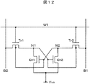
図12と図13には、プロセッサと同一チップ上に形成されるメモリセルの例を示す。
In the present invention, the BG is independently controlled as shown in FIG. 10 for the logic circuit grouped as CKT in FIG. In general, a system LSI is made up of many circuit blocks, but not all circuit blocks are operating at all times, and the parts that operate temporally and spatially are part of many circuit blocks. This will change from moment to moment. Therefore, only the circuit block to be activated has a high on-current, and many non-activated circuit blocks have a very low off-current, thereby achieving high speed, low power, and low leakage. be able to. Furthermore, since the back gate is driven from outside this circuit block, the operation of this circuit block proceeds, so that each circuit in the CKT does not drive the back gate. Since the wiring is short inside the circuit block, the load driven by each circuit is almost determined by the gate capacitance. Therefore, it is important not to increase the gate capacitance, and this is achieved.
12 and 13 show examples of memory cells formed on the same chip as the processor.
図12は、4つのトランジスタTr1,Tr2,Dr1,Dr2で構成したSRAMの例であり、Tr1とTr2のバックゲートを、メモリセルの内部ノードであるN1とN2で制御している。B1とB2は信号を読み出すビット線であり、W1がワード線である。この構成によれば、Tr1とTr2の内、必要な片方のMOSのしきい値電圧を高く、他方を低く設定することができ、このメモリセルの電力を下げることができる。 FIG. 12 shows an example of an SRAM constituted by four transistors Tr1, Tr2, Dr1, Dr2. The back gates of Tr1 and Tr2 are controlled by N1 and N2 which are internal nodes of the memory cell. B1 and B2 are bit lines for reading signals, and W1 is a word line. According to this configuration, the required threshold voltage of one of the transistors Tr1 and Tr2 can be set high and the other can be set low, and the power of the memory cell can be reduced.
図13には、6つのトランジスタTr1,Tr2,Ld1,Ld2,Dr1,Dr2で構成したSRAMの例であり、Ld1とDr1のバックゲートがそのゲートと接続され、同様にLd2とDr2のバックゲートがそのゲートと接続された構成を取る。この構成によれば、このメモリセルの安定度を高めることができる。 FIG. 13 shows an example of an SRAM composed of six transistors Tr1, Tr2, Ld1, Ld2, Dr1, and Dr2. The back gates of Ld1 and Dr1 are connected to the gates. Similarly, the back gates of Ld2 and Dr2 are connected to each other. Take the configuration connected to the gate. According to this configuration, the stability of the memory cell can be increased.
図14〜図16は、本発明を用いたプロセッサで構成される大型計算機の構成例を示す図である。 FIG. 14 to FIG. 16 are diagrams showing a configuration example of a large-sized computer constituted by a processor using the present invention.
図14において、各プロセッサは、図1のCHIP又は図15に示すプロセッサである。この図14の例では、4つのプロセッサ、プロセッサ0〜プロセッサ3がひとつのノードを形成し、このノードM個(ノード1〜ノードM−1)がネットワークで形成されている。このプロセッサ0〜プロセッサ3は、同種のプロセッサが4つでも、或いは異なるプロセッサの組み合わせでも良い。このような構成の大型計算機は並列計算に向いており、各ノードに分配された必要な計算が、4つのプロセッサで同時に処理される。この時、例えば、プロセッサ0が、全体の計算のスケジューリングや他のノードとの通信処理を受け持つ。
In FIG. 14, each processor is the CHIP in FIG. 1 or the processor shown in FIG. In the example of FIG. 14, four processors,
図15は、プロセッサの他の構成例を示す実施例である。CPUと複数のアクセラレータ1〜アクセラレータnを備えている。OtherはIO回路含めた他の回路ブロックを示す。また、キャッシュッメモリを備え、外部のメモリを制御するメモリコントローラを備えている。このメモリコントローラの動作状態によって、このプロセッサがどの階層のメモリを扱っているのかを認識し、本発明では、外部メモリ(主記憶)の先頭アクセスを探している期間は、このプロセッサ上の少なくとも一部の回路のクロック及びバックゲートを制御する。このために、クロック発生及び制御とPLLとバックゲート電圧発生回路を備えている。この図15のプロセッサが、プロセッサ0〜プロセッサ3のひとつひとつに対応する。図15の本実施例によれば、複数のアクセラレータ1〜アクセラレータnを備えた高い処理性能を持つ計算機においても、その性能を損なうことなく、電力を削減できる半導体装置を実現ですきる。
FIG. 15 is an embodiment showing another configuration example of the processor. A CPU and a plurality of
図16に、図15のプロセッサを用いて、図14の計算機を構成したときの全体像を示す。各プロセッサは図15と同じものである。この図では、メモリコントローラに接続される主記憶であるメモリが示されている。このメモリの先頭アドレスを検出するときの動作においては、本実施例では、プロセッサの少なくとも一部のバックゲートや周波数を変化させて低電力とすることはできる特徴がある。更に、各プロセッサは4つごとにネットワークI/Fでひとつのノードとなり、これがM個接続されている。また、本実施例では他の特徴として、例えば、プロセッサ0が、他のプロセッサ1〜3の状態を制御することができる。例えば、他のノードとの通信のような時は、プロセッサ0のみが動作すれば良く、この時他のプロセッサのバックゲートや周波数に指令を与えることができる。
FIG. 16 shows an overall image when the computer of FIG. 14 is configured using the processor of FIG. Each processor is the same as in FIG. In this figure, a memory which is a main memory connected to the memory controller is shown. In this operation when detecting the start address of the memory, this embodiment has a feature that low power can be obtained by changing the back gate or frequency of at least a part of the processor. Further, every four processors form one node in the network I / F, and M processors are connected. In this embodiment, as another feature, for example, the
本発明は、半導体装置に係わり、高速処理計算を行うが電力の増大が問題となっているサーバやスーパーコンピュータなどの分野において、処理速度の低下をおこさずに消費電力を低下させることができる装置を実現するものである。 The present invention relates to a semiconductor device, and can reduce power consumption without reducing the processing speed in a field such as a server or a supercomputer that performs high-speed processing calculations but has an increase in power. Is realized.
DCL…論理回路ブロック、BAC…バックゲート制御信号発生回路ブロック、PFC…出力バッファ回路ブロック、UTB…埋め込み酸化膜、OX…ゲート酸化膜、STI…溝堀型絶縁領域、SSTI…溝堀型絶縁領域(STIよりも浅い)、TB…埋め込み酸化膜(UTBの下層にある)。 DCL: logic circuit block, BAC: back gate control signal generation circuit block, PFC: output buffer circuit block, UTB: buried oxide film, OX: gate oxide film, STI: grooved insulation region, SSTI ... grooved insulation region (Shallow than STI), TB ... buried oxide (under the UTB).
Claims (8)
前記演算処理装置で使用される命令及びデータを含む記憶情報を蓄えた、アクセス速度が前記演算処理装置の動作速度よりも遅い大容量記憶装置と、
前記記憶情報の少なくとも一部を蓄えた、アクセス速度が前記演算処理装置の動作速度よりも遅く、前記大容量記憶装置のアクセス速度よりも速い小規模記憶装置と、
前記大容量記憶装置を制御する記憶制御装置と、を有し、
前記演算処理装置が、ゲート端子とドレイン端子とソース端子と基板端子とを具備してなるCMOSトランジスタで構成され、
前記CMOSトランジスタの基板端子に、前記小規模記憶装置に記憶された記憶情報が前記演算処理装置において実行される第1の期間では第1の電圧が印加され、
前記大容量記憶装置が、前記演算処理装置で必要な記憶情報を前記演算処理装置へ送る準備を行う第2の期間では第2の電圧が印加され、
前記第1の電圧と前記第2の電圧とは異なる電圧であって、前記第1の電圧は前記CMOSトランジスタのしきい値電圧の絶対値を大きくする電圧であることを特徴とする半導体装置。 An arithmetic processing unit;
A large-capacity storage device that stores storage information including instructions and data used in the arithmetic processing device and whose access speed is slower than the operation speed of the arithmetic processing device;
A small-scale storage device that stores at least a part of the storage information, and whose access speed is slower than the operation speed of the arithmetic processing device and faster than the access speed of the mass storage device;
A storage control device for controlling the mass storage device,
The arithmetic processing unit is composed of a CMOS transistor having a gate terminal, a drain terminal, a source terminal, and a substrate terminal,
A first voltage is applied to the substrate terminal of the CMOS transistor in a first period in which the storage information stored in the small-scale storage device is executed in the arithmetic processing unit,
A second voltage is applied in a second period in which the mass storage device prepares to send storage information required by the arithmetic processing device to the arithmetic processing device,
The semiconductor device, wherein the first voltage and the second voltage are different voltages, and the first voltage is a voltage that increases an absolute value of a threshold voltage of the CMOS transistor.
前記第2の期間において、前記バックゲート端子に、前記CMOSトランジスタのしきい値電圧の絶対値を大きくする電圧であって、前記第1の期間とは異なる電圧が印加されることを特徴とする請求項1記載の半導体装置。 The CMOS transistor has an SOI structure formed on an insulating film, and a gate terminal, a drain terminal, a source terminal, a semiconductor region provided under the insulating film, and a voltage applied to the semiconductor region With a back gate terminal that can
In the second period, a voltage that increases the absolute value of the threshold voltage of the CMOS transistor and is different from that in the first period is applied to the back gate terminal. The semiconductor device according to claim 1.
前記演算処理装置が使用する命令及びデータを含む記憶情報を蓄えた、アクセス速度が前記演算処理装置の動作速度よりも遅い大容量記憶装置と、
前記記憶情報の少なくとも一部を蓄えた、アクセス速度が前記演算処理装置の動作速度よりも遅く、前記大容量記憶装置のアクセス速度よりも速い小規模記憶装置と、
前記大容量記憶装置を制御する記憶制御装置と、を有し、
前記演算処理装置が、ゲート端子とドレイン端子とソース端子と基板端子とを具備してなるCMOSトランジスタで構成され、
前記演算処理装置が前記小規模記憶装置に記憶された記憶情報を用いて演算を実行する第1の期間において、前記CMOSトランジスタの基板端子に第1の電圧が印加され、前記演算処理装置は第1のクロック周波数に同期して動作し、
前記大容量記憶装置が、前記演算処理装置に必要な記憶情報を前記演算処理装置へ送る準備を行う第2の期間において、前記演算処理装置は前記第1のクロック周波数より遅い周波数を有する第2のクロック周波数に同期して動作し、前記基板端子には、前記CMOSトランジスタのしきい値電圧の絶対値を大きくする前記第1の電圧とは異なる第2の電圧が印加されることを特徴とする半導体装置。 An arithmetic processing unit;
A large-capacity storage device that stores storage information including instructions and data used by the arithmetic processing device and whose access speed is slower than the operation speed of the arithmetic processing device;
A small-scale storage device that stores at least a part of the storage information, and whose access speed is slower than the operation speed of the arithmetic processing device and faster than the access speed of the mass storage device;
A storage control device for controlling the mass storage device,
The arithmetic processing unit is composed of a CMOS transistor having a gate terminal, a drain terminal, a source terminal, and a substrate terminal,
In a first period in which the arithmetic processing unit performs an operation using stored information stored in the small-scale storage device, a first voltage is applied to the substrate terminal of the CMOS transistor, and the arithmetic processing unit Operates in synchronization with the clock frequency of 1,
In a second period in which the mass storage device prepares to send storage information necessary for the arithmetic processing device to the arithmetic processing device, the arithmetic processing device has a second frequency that is slower than the first clock frequency. The second voltage different from the first voltage for increasing the absolute value of the threshold voltage of the CMOS transistor is applied to the substrate terminal. Semiconductor device.
前記第2の期間において、前記バックゲート端子に、前記CMOSトランジスタのしきい値電圧の絶対値を大きくする電圧であって、前記第1の期間とは異なる電圧が印加されることを特徴とする請求項5記載の半導体装置。 The CMOS transistor has an SOI structure formed on an insulating film, and a gate terminal, a drain terminal, a source terminal, a semiconductor region provided under the insulating film, and a voltage applied to the semiconductor region With a back gate terminal that can
In the second period, a voltage that increases the absolute value of the threshold voltage of the CMOS transistor and is different from that in the first period is applied to the back gate terminal. The semiconductor device according to claim 5.
Priority Applications (1)
| Application Number | Priority Date | Filing Date | Title |
|---|---|---|---|
| JP2008325702A JP4966956B2 (en) | 2008-12-22 | 2008-12-22 | Semiconductor device |
Applications Claiming Priority (1)
| Application Number | Priority Date | Filing Date | Title |
|---|---|---|---|
| JP2008325702A JP4966956B2 (en) | 2008-12-22 | 2008-12-22 | Semiconductor device |
Publications (2)
| Publication Number | Publication Date |
|---|---|
| JP2010146474A true JP2010146474A (en) | 2010-07-01 |
| JP4966956B2 JP4966956B2 (en) | 2012-07-04 |
Family
ID=42566816
Family Applications (1)
| Application Number | Title | Priority Date | Filing Date |
|---|---|---|---|
| JP2008325702A Expired - Fee Related JP4966956B2 (en) | 2008-12-22 | 2008-12-22 | Semiconductor device |
Country Status (1)
| Country | Link |
|---|---|
| JP (1) | JP4966956B2 (en) |
Cited By (1)
| Publication number | Priority date | Publication date | Assignee | Title |
|---|---|---|---|---|
| JP2015148890A (en) * | 2014-02-05 | 2015-08-20 | 富士通株式会社 | Information processor, information processing system, and control method for information processing system |
Citations (7)
| Publication number | Priority date | Publication date | Assignee | Title |
|---|---|---|---|---|
| WO1998022863A1 (en) * | 1996-11-21 | 1998-05-28 | Hitachi, Ltd. | Low-power processor |
| JP2000214967A (en) * | 1998-11-20 | 2000-08-04 | Hitachi Ltd | Low-electric-power information processor |
| JP2002006979A (en) * | 2000-06-19 | 2002-01-11 | Seiko Epson Corp | Clock control device, semiconductor intedrated circuit device, micro computer, and electronic equipment |
| JP2005115769A (en) * | 2003-10-09 | 2005-04-28 | Nec Corp | Information processor |
| JP2005196430A (en) * | 2004-01-07 | 2005-07-21 | Hiroshi Nakamura | Semiconductor device and method for controlling source voltage/clock frequency thereof |
| JP2007042730A (en) * | 2005-08-01 | 2007-02-15 | Renesas Technology Corp | Semiconductor device and semiconductor integrated circuit using the same |
| JP2007193433A (en) * | 2006-01-17 | 2007-08-02 | Matsushita Electric Ind Co Ltd | Information processor |
-
2008
- 2008-12-22 JP JP2008325702A patent/JP4966956B2/en not_active Expired - Fee Related
Patent Citations (7)
| Publication number | Priority date | Publication date | Assignee | Title |
|---|---|---|---|---|
| WO1998022863A1 (en) * | 1996-11-21 | 1998-05-28 | Hitachi, Ltd. | Low-power processor |
| JP2000214967A (en) * | 1998-11-20 | 2000-08-04 | Hitachi Ltd | Low-electric-power information processor |
| JP2002006979A (en) * | 2000-06-19 | 2002-01-11 | Seiko Epson Corp | Clock control device, semiconductor intedrated circuit device, micro computer, and electronic equipment |
| JP2005115769A (en) * | 2003-10-09 | 2005-04-28 | Nec Corp | Information processor |
| JP2005196430A (en) * | 2004-01-07 | 2005-07-21 | Hiroshi Nakamura | Semiconductor device and method for controlling source voltage/clock frequency thereof |
| JP2007042730A (en) * | 2005-08-01 | 2007-02-15 | Renesas Technology Corp | Semiconductor device and semiconductor integrated circuit using the same |
| JP2007193433A (en) * | 2006-01-17 | 2007-08-02 | Matsushita Electric Ind Co Ltd | Information processor |
Cited By (2)
| Publication number | Priority date | Publication date | Assignee | Title |
|---|---|---|---|---|
| JP2015148890A (en) * | 2014-02-05 | 2015-08-20 | 富士通株式会社 | Information processor, information processing system, and control method for information processing system |
| US9710047B2 (en) | 2014-02-05 | 2017-07-18 | Fujitsu Limited | Apparatus, system, and method for varying a clock frequency or voltage during a memory page transfer |
Also Published As
| Publication number | Publication date |
|---|---|
| JP4966956B2 (en) | 2012-07-04 |
Similar Documents
| Publication | Publication Date | Title |
|---|---|---|
| US20200089407A1 (en) | Inter zone write for zoned namespaces | |
| KR101249648B1 (en) | Semiconductor device and semiconductor integrated circuit using the same | |
| US7683669B2 (en) | Semiconductor device, CPU, image processing circuit and electronic device, and driving method of semiconductor device | |
| US9703704B2 (en) | Semiconductor device | |
| JP2020042892A (en) | Semiconductor device and dynamic logic circuit | |
| US9886997B2 (en) | Semiconductor device for reducing an instantaneous voltage drop | |
| Shuto et al. | Nonvolatile static random access memory based on spin-transistor architecture | |
| JP5364125B2 (en) | Semiconductor device | |
| JP6420165B2 (en) | Semiconductor device | |
| JP2019046199A (en) | Processor and electronic device | |
| WO2009092163A1 (en) | Operational mode control in serial-connected memory based on identifier | |
| TW459230B (en) | Static RAM having word line driving circuitry shared by all the memory cells provided therein | |
| JP2009266339A (en) | Semiconductor memory device and electronic device using same | |
| JP4966956B2 (en) | Semiconductor device | |
| WO2023138219A1 (en) | Memory, timing control method, and electronic device | |
| Kawahara et al. | Green computing with emerging memory | |
| Shastri et al. | Read write stability with leakage minimization of 4t SRAM cell for nano CMOS technology | |
| JP4972634B2 (en) | Semiconductor device | |
| Sakthimurugan et al. | Designing low power magentic flip flop in 45 nm FDSOI technology for large scale cluster based engineering application | |
| Akashe et al. | Read write stability of Dual-VT 7T SRAM Cell at 45 nm technology | |
| US20230317145A1 (en) | Method and apparatus to implement an integrated circuit to operate based on data access characteristics | |
| US20230315331A1 (en) | Method and apparatus to implement an integrated circuit including both dynamic random-access memory (dram) and static random-access memory (sram) | |
| Srivastava et al. | Effect of technology scale-down on power reduction strategies | |
| Rahman et al. | A new Tunnel-FET based RAM concept for ultra-low power applications | |
| Yadavalli et al. | Design of High-Speed SRAM Cell Using FinFET Technology |
Legal Events
| Date | Code | Title | Description |
|---|---|---|---|
| A977 | Report on retrieval |
Free format text: JAPANESE INTERMEDIATE CODE: A971007 Effective date: 20111031 |
|
| A131 | Notification of reasons for refusal |
Free format text: JAPANESE INTERMEDIATE CODE: A131 Effective date: 20111213 |
|
| A521 | Written amendment |
Free format text: JAPANESE INTERMEDIATE CODE: A523 Effective date: 20120213 |
|
| TRDD | Decision of grant or rejection written | ||
| A01 | Written decision to grant a patent or to grant a registration (utility model) |
Free format text: JAPANESE INTERMEDIATE CODE: A01 Effective date: 20120306 |
|
| A01 | Written decision to grant a patent or to grant a registration (utility model) |
Free format text: JAPANESE INTERMEDIATE CODE: A01 |
|
| A61 | First payment of annual fees (during grant procedure) |
Free format text: JAPANESE INTERMEDIATE CODE: A61 Effective date: 20120402 |
|
| R150 | Certificate of patent or registration of utility model |
Free format text: JAPANESE INTERMEDIATE CODE: R150 |
|
| FPAY | Renewal fee payment (event date is renewal date of database) |
Free format text: PAYMENT UNTIL: 20150406 Year of fee payment: 3 |
|
| LAPS | Cancellation because of no payment of annual fees |