JP2010141211A - Semiconductor device - Google Patents
Semiconductor device Download PDFInfo
- Publication number
- JP2010141211A JP2010141211A JP2008317583A JP2008317583A JP2010141211A JP 2010141211 A JP2010141211 A JP 2010141211A JP 2008317583 A JP2008317583 A JP 2008317583A JP 2008317583 A JP2008317583 A JP 2008317583A JP 2010141211 A JP2010141211 A JP 2010141211A
- Authority
- JP
- Japan
- Prior art keywords
- insulating film
- region
- interlayer insulating
- semiconductor layer
- electrode
- Prior art date
- Legal status (The legal status is an assumption and is not a legal conclusion. Google has not performed a legal analysis and makes no representation as to the accuracy of the status listed.)
- Pending
Links
Images


Abstract
Description
本発明は半導体装置に関する。 The present invention relates to a semiconductor device.
薄膜トランジスタ(Thin Film Transistor:TFT)の設けられた半導体装置は、表示装置のアクティブマトリクス基板の一部として好適に用いられている。例えば、アクティブマトリクス基板を備える液晶表示装置は、テレビ、コンピュータ、デジタルカメラ、携帯端末等のディスプレイに利用されている。 A semiconductor device provided with a thin film transistor (TFT) is preferably used as a part of an active matrix substrate of a display device. For example, a liquid crystal display device including an active matrix substrate is used for a display of a television, a computer, a digital camera, a portable terminal, or the like.
アクティブマトリクス基板では、画素領域にTFTを設けるだけでなく周辺領域に駆動回路や配線等を一体的に設けることが検討されている。このようなアクティブマトリクス基板に用いられる半導体装置には、TFTだけでなく容量結合部や端子部が形成される(例えば、特許文献1参照)。 In an active matrix substrate, it is considered that not only a TFT is provided in a pixel region but also a driving circuit and wiring are integrally provided in a peripheral region. In a semiconductor device used for such an active matrix substrate, not only a TFT but also a capacitive coupling portion and a terminal portion are formed (for example, see Patent Document 1).
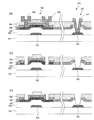
特許文献1には、ボトムゲート構造のTFTを備える半導体装置が開示されている。半導体装置900には、TFT920、コンタクト部940および容量結合部960が設けられている。
Patent Document 1 discloses a semiconductor device including a bottom-gate TFT. The
以下、図15および図16を参照して、特許文献1の半導体装置900の製造方法を説明する。
Hereinafter, a method for manufacturing the
まず、図15(a)に示すように、絶縁基板901上に、ゲート電極922、ソース配線932、下側電極942および下側配線962を同一工程で形成する。ゲート電極922、ソース配線932、下側電極942および下側配線962のそれぞれは同じ材料から形成されている。
First, as shown in FIG. 15A, a
次に、図15(b)に示すように、半導体装置900では、ソース配線932および下側電極942にメッキ処理を行い、ソース配線932および下側電極942上にCu被膜933、943を形成する。
Next, as illustrated in FIG. 15B, in the
次に、図15(c)に示すように、ゲート電極922、Cu被膜933、Cu被膜943および下側配線962を覆う絶縁層925を堆積し、絶縁層925上に第1半導体層Se1および第2半導体層Se2を堆積する。第1半導体層Se1は非晶質シリコンから形成されており、第2半導体層Se2はドーパントを含有する非晶質シリコンから形成されている。
Next, as shown in FIG. 15C, an
次に、図15(d)に示すように、第2半導体層Se2を覆うフォトレジストマスクPxを形成し、フォトレジストマスクPxを利用してエッチングを行う。フォトレジストマスクPxは、TFT領域および容量結合領域において第2半導体層Seを覆うように設けられている。エッチングにより、TFT領域において第1半導体層Se1から第1半導体層926aが形成され、第2半導体層Se2から第2半導体層926bが形成される。同様に、エッチングにより、容量結合領域において第1半導体層Se1から第1半導体層966aが形成され、第2半導体層Se2から第2半導体層966bが形成される。このように、半導体層926、966はそれぞれ積層構造である。
Next, as shown in FIG. 15D, a photoresist mask Px covering the second semiconductor layer Se2 is formed, and etching is performed using the photoresist mask Px. The photoresist mask Px is provided so as to cover the second semiconductor layer Se in the TFT region and the capacitive coupling region. By etching, the
次に、図15(e)に示すように、フォトレジストマスクPxを剥離し、絶縁層925および半導体層926、966を覆うフォトレジストマスクPyを形成し、フォトレジストマスクPyを利用してエッチングを行う。フォトレジストマスクPyはTFT領域のゲート電極922上方部分において開口しており、エッチングにより、第2半導体層926bのチャネル領域部分が除去される。このため、第1半導体層926aのソース領域はチャネル領域を介してドレイン領域と連続しているが、第2半導体層926bのうちチャネル領域に相当する領域は除去されており、第2半導体層926bのソース領域はドレイン領域と不連続である。
Next, as shown in FIG. 15E, the photoresist mask Px is peeled off, a photoresist mask Py covering the
次に、図16(f)に示すように、フォトレジストマスクPyを剥離し、絶縁層925および半導体層926、966を覆う第1層間絶縁膜902を堆積する。
Next, as shown in FIG. 16F, the photoresist mask Py is removed, and a first
次に、図16(g)に示すように、第1層間絶縁膜902を覆う第2層間絶縁膜904を堆積し、第2層間絶縁膜904上にフォトレジストマスクPzを形成する。その後、フォトレジストマスクPzを利用してコンタクトホールを形成する。このエッチングにより、TFT領域において第1、第2層間絶縁膜902、904にコンタクトホールが形成され、半導体層926のソース領域およびドレイン領域の一部が露出する。また、このエッチングにより、コンタクト領域において第1、第2層間絶縁膜902、904および絶縁層925にコンタクトホールが形成され、Cu被覆943の一部が露出する。また、ソース配線領域においても同様に、第1、第2層間絶縁膜902、904および絶縁層925にコンタクトホールが形成され、Cu被覆933の一部が露出する。
Next, as shown in FIG. 16G, a second
次に、図16(h)に示すように、第2層間絶縁膜904上に画素電極908を形成する。画素電極908は、TFT領域と容量結合領域との間に設けられている。
Next, as illustrated in FIG. 16H, the
次に、図16(i)に示すように、フォトレジストマスクPzを剥離し、ソース電極928、ドレイン電極930、上側電極942、第1上側配線962aおよび第2上側配線962bを形成する。ソース電極928、ドレイン電極930、上側電極942、第1上側配線962aおよび第2上側配線962bは、同一工程で形成される。
Next, as shown in FIG. 16I, the photoresist mask Pz is peeled off to form a
以上のようにして半導体装置900は作製される。なお、半導体装置900では、メッキ処理を行うことにより、配線抵抗の増加を抑制するとともに消費電力の増加が抑制されている。
特許文献1の半導体装置では、メッキ処理を行うことを必須としており、製造工程および製造時間が増加することになる。また、特許文献1の半導体装置では、TFT領域において第1、第2層間絶縁膜902、904を除去するエッチングにより、コンタクト部において第1、第2層間絶縁膜902、904だけでなく絶縁層925の除去も行っている。このように、同一のエッチング工程で深さの異なるコンタクトホールを形成する場合、適切なコンタクトホールを形成することができず、接続不良が発生することがある。なお、特許文献1には、第2層間絶縁膜904の表面が平坦化されているように図示されており、第2層間絶縁膜904の厚さは第2層間絶縁膜904の下方に設けられた構成要素に応じて大きく変動しているようにみえるが、特に、第2層間絶縁膜904が比較的薄い場合、第2層間絶縁膜904の表面は平坦にはならず、第2層間絶縁膜904の厚さは下方の構成要素にかかわらずほぼ一定となるか、あるいは、第2層間絶縁膜904の厚さの変動量は下方の構成要素の厚さの差よりも小さい。
In the semiconductor device of Patent Document 1, it is essential to perform the plating process, which increases the manufacturing process and manufacturing time. Further, in the semiconductor device disclosed in Patent Document 1, not only the first and second
本発明は、上記課題を鑑みてなされたものであり、その目的は、接続不良を抑制した半導体装置を提供することにある。 The present invention has been made in view of the above problems, and an object of the present invention is to provide a semiconductor device in which poor connection is suppressed.
本発明による半導体装置は、ゲート電極と、前記ゲート電極と同じ材料から形成された下側電極と、前記ゲート電極および前記下側電極を覆う絶縁層と、ソース領域、チャネル領域およびドレイン領域を有する半導体層であって、前記チャネル領域が前記絶縁層を介して前記ゲート電極と対向する、半導体層と、前記絶縁層の一部および前記半導体層を覆う第1層間絶縁膜であって、前記絶縁層のうちの前記下側電極上の領域を覆わない第1層間絶縁膜と、前記絶縁層および前記第1層間絶縁膜を覆う第2層間絶縁膜と、前記第1層間絶縁膜および前記第2層間絶縁膜に設けられたコンタクトホールを介して前記半導体層の前記ソース領域と電気的に接続されたソース電極と、前記第1層間絶縁膜および前記第2層間絶縁膜に設けられたコンタクトホールを介して前記半導体層の前記ドレイン領域と電気的に接続されたドレイン電極と、前記ソース電極および前記ドレイン電極と同じ材料から形成された上側電極であって、前記絶縁層および前記第2層間絶縁膜に設けられたコンタクトホールを介して前記下側電極と電気的に接続された上側電極とを備える。 A semiconductor device according to the present invention includes a gate electrode, a lower electrode made of the same material as the gate electrode, an insulating layer covering the gate electrode and the lower electrode, a source region, a channel region, and a drain region. A semiconductor layer, wherein the channel region is opposed to the gate electrode through the insulating layer, and is a first interlayer insulating film covering a part of the insulating layer and the semiconductor layer, the insulating layer A first interlayer insulating film that does not cover a region of the layer on the lower electrode; a second interlayer insulating film that covers the insulating layer and the first interlayer insulating film; and the first interlayer insulating film and the second A source electrode electrically connected to the source region of the semiconductor layer through a contact hole provided in the interlayer insulating film, and a capacitor provided in the first interlayer insulating film and the second interlayer insulating film. A drain electrode electrically connected to the drain region of the semiconductor layer through a hole, and an upper electrode formed of the same material as the source electrode and the drain electrode, wherein the insulating layer and the second interlayer And an upper electrode electrically connected to the lower electrode through a contact hole provided in the insulating film.
ある実施形態において、前記半導体装置は、前記ゲート電極および前記下側電極と同じ材料から形成された下側配線と、前記ソース電極、前記ドレイン電極および前記上側電極と同じ材料から形成された上側配線であって、前記絶縁層、前記第1層間絶縁膜および前記第2層間絶縁膜を介して前記下側配線と対向する上側配線とをさらに備える。 In one embodiment, the semiconductor device includes a lower wiring formed from the same material as the gate electrode and the lower electrode, and an upper wiring formed from the same material as the source electrode, the drain electrode, and the upper electrode. And an upper wiring facing the lower wiring via the insulating layer, the first interlayer insulating film, and the second interlayer insulating film.
ある実施形態において、前記半導体層は、前記ソース領域と前記チャネル領域との間に位置する第1中間領域と、前記チャネル領域と前記ドレイン領域との間に位置する第2中間領域とをさらに有しており、前記半導体層の前記ソース領域および前記ドレイン領域のそれぞれにはドーパントがドープされており、前記第1中間領域には、前記ソース領域よりも低濃度のドーパントがドープされており、前記第2中間領域には、前記ドレイン領域よりも低濃度のドーパントがドープされている。 In one embodiment, the semiconductor layer further includes a first intermediate region located between the source region and the channel region, and a second intermediate region located between the channel region and the drain region. Each of the source region and the drain region of the semiconductor layer is doped with a dopant, and the first intermediate region is doped with a dopant at a lower concentration than the source region, The second intermediate region is doped with a dopant having a lower concentration than the drain region.
ある実施形態において、前記半導体層の前記ソース領域および前記ドレイン領域のそれぞれは、前記第1層間絶縁膜で覆われており、前記第1中間領域および前記第2中間領域のそれぞれは、前記第2層間絶縁膜で覆われている。 In one embodiment, each of the source region and the drain region of the semiconductor layer is covered with the first interlayer insulating film, and each of the first intermediate region and the second intermediate region is the second intermediate region. It is covered with an interlayer insulating film.
ある実施形態において、前記半導体層の前記チャネル領域上に前記第1層間絶縁膜が設けられている。 In one embodiment, the first interlayer insulating film is provided on the channel region of the semiconductor layer.
ある実施形態において、前記半導体層の前記チャネル領域上に前記第2層間絶縁膜が設けられている。 In one embodiment, the second interlayer insulating film is provided on the channel region of the semiconductor layer.
本発明による半導体装置の製造方法は、下側導電層を堆積し、前記下側導電層からゲート電極および下側電極を形成する工程と、前記ゲート電極および前記下側電極を覆う絶縁層を形成する工程と、ソース領域、チャネル領域およびドレイン領域を有する半導体層を形成する工程であって、前記チャネル領域は前記絶縁層を介して前記ゲート電極と対向する、工程と、前記絶縁層および前記半導体層を覆う第1層間絶縁膜を堆積する工程と、前記第1層間絶縁膜のうち少なくとも前記下側電極と対向する部分を除去するように前記第1層間絶縁膜のエッチングを行う工程と、前記絶縁層および前記第1層間絶縁膜を覆う第2層間絶縁膜を堆積する工程と、前記半導体層のうちの前記ソース領域および前記ドレイン領域のそれぞれの少なくとも一部が露出するように前記第1層間絶縁膜および前記第2層間絶縁膜にコンタクトホールを形成するとともに、前記下側電極が露出するように前記絶縁層および前記第2層間絶縁膜にコンタクトホールを形成する工程と、前記コンタクトホールを形成した後に上側導電層を堆積し、前記上側導電層から、前記半導体層の前記ソース領域および前記ドレイン領域とそれぞれ電気的に接続されたソース電極およびドレイン電極を形成するとともに前記下側電極と電気的に接続された上側電極を形成する工程とを包含する。 A method of manufacturing a semiconductor device according to the present invention includes a step of depositing a lower conductive layer, forming a gate electrode and a lower electrode from the lower conductive layer, and forming an insulating layer covering the gate electrode and the lower electrode And a step of forming a semiconductor layer having a source region, a channel region, and a drain region, wherein the channel region faces the gate electrode through the insulating layer, and the insulating layer and the semiconductor Depositing a first interlayer insulating film covering the layer; etching the first interlayer insulating film so as to remove at least a portion of the first interlayer insulating film facing the lower electrode; Depositing a second interlayer insulating film covering the insulating layer and the first interlayer insulating film; and at least each of the source region and the drain region of the semiconductor layer Contact holes are formed in the first interlayer insulating film and the second interlayer insulating film so as to be exposed, and contact holes are formed in the insulating layer and the second interlayer insulating film so that the lower electrode is exposed. Forming an upper conductive layer after forming the contact hole, and forming a source electrode and a drain electrode electrically connected to the source region and the drain region of the semiconductor layer from the upper conductive layer, respectively. Forming an upper electrode electrically connected to the lower electrode.
ある実施形態において、前記コンタクトホールを形成する工程は、ドライエッチングを行う工程を含む。 In one embodiment, the step of forming the contact hole includes a step of performing dry etching.
ある実施形態において、前記製造方法は、前記下側導電層から下側配線を形成する工程と、前記上側導電層から、前記絶縁層、前記第1層間絶縁膜および前記第2層間絶縁膜を介して前記下側配線と対向する上側配線を形成する工程とをさらに包含する。 In one embodiment, the manufacturing method includes a step of forming a lower wiring from the lower conductive layer, and the upper conductive layer through the insulating layer, the first interlayer insulating film, and the second interlayer insulating film. And a step of forming an upper wiring facing the lower wiring.
ある実施形態において、前記半導体層は、前記ソース領域と前記チャネル領域との間に設けられた第1中間領域と、前記チャネル領域と前記ドレイン領域との間に設けられた第2中間領域とをさらに有しており、前記製造方法は、前記半導体層の前記チャネル領域、前記第1中間領域および前記第2中間領域と重なるとともに前記半導体層の前記ソース領域および前記ドレイン領域と重ならないフォトレジストマスクを利用して第1ドーピングを行う工程と、前記半導体層のうちの少なくとも前記チャネル領域と重なるとともに前記半導体層のうちの少なくとも前記第1中間領域および前記第2中間領域と重ならないフォトレジストマスクを利用して第2ドーピングを行う工程とをさらに包含する。 In one embodiment, the semiconductor layer includes a first intermediate region provided between the source region and the channel region, and a second intermediate region provided between the channel region and the drain region. The manufacturing method further includes a photoresist mask that overlaps the channel region, the first intermediate region, and the second intermediate region of the semiconductor layer and that does not overlap the source region and the drain region of the semiconductor layer. And a photoresist mask that overlaps at least the channel region of the semiconductor layer and does not overlap at least the first intermediate region and the second intermediate region of the semiconductor layer. And further performing a second doping process.
ある実施形態において、前記第1層間絶縁膜のエッチングを行う工程は、前記第1層間絶縁膜のうち、少なくとも、前記半導体層の前記第1中間領域および前記第2中間領域のそれぞれに対応する領域を除去する工程を含む。 In one embodiment, the step of etching the first interlayer insulating film includes at least a region of the first interlayer insulating film corresponding to each of the first intermediate region and the second intermediate region of the semiconductor layer. The process of removing.
ある実施形態において、前記第1層間絶縁膜のエッチングは、前記第2ドーピングを行う前または前記第1ドーピングを行った後に、前記第2ドーピングのフォトレジストマスクを利用して行われる。 In one embodiment, the etching of the first interlayer insulating film is performed using the photoresist mask of the second doping before the second doping or after the first doping.
ある実施形態において、前記半導体層の少なくともチャネル領域を覆わないフォトレジストマスクを利用してチャネルドーピングを行う工程をさらに包含し、前記第1層間絶縁膜のエッチングは、前記チャネルドーピングを行う前または前記チャネルドーピングを行った後に、前記チャネルドーピングのフォトレジストマスクを利用して行われる。 In one embodiment, the method further includes a step of performing channel doping using a photoresist mask that does not cover at least a channel region of the semiconductor layer, and the etching of the first interlayer insulating film is performed before the channel doping or After channel doping, the channel doping is performed using a photoresist mask.
本発明によれば、接続不良を抑制した半導体装置を提供できる。 ADVANTAGE OF THE INVENTION According to this invention, the semiconductor device which suppressed the connection failure can be provided.
以下、図面を参照して、本発明による半導体装置の実施形態を説明する。ただし、本発明は、以下の実施形態に限定されるものではない。 Hereinafter, embodiments of a semiconductor device according to the present invention will be described with reference to the drawings. However, the present invention is not limited to the following embodiments.
(実施形態1)
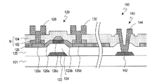
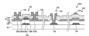
以下、図1を参照して本発明による半導体装置の第1実施形態を説明する。図1に、本実施形態の半導体装置100の模式図を示す。
(Embodiment 1)
Hereinafter, a semiconductor device according to a first embodiment of the present invention will be described with reference to FIG. FIG. 1 shows a schematic diagram of a
半導体装置100にはTFT120およびコンタクト部140が設けられている。TFT120はボトムゲート構造を有している。TFT120は例えばNチャネルトランジスタである。
The
TFT120は、ゲート電極122と、ゲート電極122を覆うゲート絶縁膜124と、ゲート絶縁膜124上に設けられた半導体層126と、ソース電極128と、ドレイン電極130とを有している。ゲート絶縁膜124は絶縁層125の一部である。例えば、絶縁層125はSiO2から形成されており、その厚さは250nmである。
The
半導体層126は例えば多結晶半導体から形成される。半導体層126非晶質状態で堆積された後、結晶化されたものであってもよい。あるいは、半導体層126は微結晶半導体または非晶質半導体から形成されてもよい。
The
半導体層126は、ソース領域126sと、チャネル領域126cと、ドレイン領域126dとを有している。チャネル領域126cはゲート絶縁膜124を介してゲート電極122と対向している。
The
チャネル領域126cにはTFT120のしきい値電圧を制御するために低濃度のBがドープされている。チャネル領域126cのドーパント濃度は例えば3×10¹²個/cm2である。
The
また、ソース領域126sおよびドレイン領域126dには比較的高濃度のドーパント(例えば、P)がドープされている。ソース領域126sおよびドレイン領域126dのドーパント濃度は例えば4×10¹⁴個/cm2である。ソース領域126sはソース電極128と電気的に接続されており、ドレイン領域126dはドレイン電極130と電気的に接続されている。
The
また、半導体層126のうち、ソース領域126sとチャネル領域126cとの間に位置する第1中間領域126a、および、チャネル領域126cとドレイン領域126dとの間に位置する第2中間領域126bのそれぞれに比較的低濃度のドーパント(例えば、P)がドープされている。第1、第2中間領域126a、126bのドーパント濃度は例えば1×10¹³個/cm2である。第1、第2中間領域126a、126bはLDD(Lightly Doped Drain)領域とも呼ばれる。また、第1、第2中間領域126a、126bは低濃度領域とも呼ばれ、ソース、ドレイン領域126s、126dは高濃度領域とも呼ばれることもある。
Further, in the
コンタクト部140は、下側電極142と、下側電極142と電気的に接続された上側電極144とを有している。下側電極142はゲート電極122とともに絶縁基板101上に設けられている。なお、絶縁基板101は透明であり、例えば、ガラス基板である。あるいは、下側電極142はゲート電極122とともに絶縁基板101上に設けられたベースコート層(図示せず)上に設けられてもよい。
The
半導体装置100は、また、絶縁層125および半導体層126を覆う第1層間絶縁膜102と、絶縁層125、半導体層126および第1層間絶縁膜102を覆う第2層間絶縁膜104とをさらに備えている。なお、以下の説明において、第1層間絶縁膜102および第2層間絶縁膜104を総称して層間絶縁膜Nと呼ぶことがある。例えば、第1層間絶縁膜102の厚さは250nmであり、第2層間絶縁膜104の厚さは250nmである。なお、第1層間絶縁膜102は第2層間絶縁膜104よりも薄くてもよい。
The
例えば、第1層間絶縁膜102はSiNから形成されており、第2層間絶縁膜104はSiO2から形成されている。第1層間絶縁膜102または第2層間絶縁膜104を形成した後、加熱処理が行われることがあるが、第1層間絶縁膜102がSiNから形成されていると、第1層間絶縁膜102に含有された水素原子が半導体層126と第1層間絶縁膜102との界面に供給され、TFT特性を劣化させる不対結合手(ダングリングボンド)が終端化して不活性化される。このようにダングリングボンドを不活性化する加熱処理は水素化アニールとも呼ばれる。また、第1層間絶縁膜102がSiNから形成されている場合、SiNの比誘電率が7.0と比較的高いため、第2層間絶縁膜104は比誘電率の比較的低い材料(例えば、比誘電率が3.9であるSiO2)から形成されていることが好ましい。これにより、層間絶縁膜NをSiNの単層膜で形成するよりも薄くすることができる。ただし、第1層間絶縁膜102がSiO2から形成され、第2層間絶縁膜104がSiNから形成されてもよい。
For example, the first
ソース電極128およびドレイン電極130は第1、第2層間絶縁膜102、104に設けられたコンタクトホールを介してソース領域126sおよびドレイン領域126dとそれぞれ電気的に接続されている。また、上側電極144は絶縁層125および第2層間絶縁膜104に設けられたコンタクトホールを介して下側電極142と電気的に接続されている。
The
ゲート電極122および下側電極142は同じ材料から形成されており、ゲート電極122および下側電極142は同一工程で形成される。以下の説明において、ゲート電極122および下側電極142を形成する導電層を下側導電層またはゲート電極層とも呼ぶ。この導電層は、例えば、W/Ta/TaNの積層構造であり、その厚さはそれぞれ10nm/100nm/30nmである。なお、積層構造のうちのTaNがガラス基板側である。
The
また、ソース電極128、ドレイン電極130および上側電極144はいずれも同じ材料から形成されており、ソース電極128、ドレイン電極130および上側電極144は同一工程で形成される。以下の説明において、ソース電極128、ドレイン電極130および上側電極144を形成する導電層を上側導電層またはソース電極層とも呼ぶ。この導電層はTi/Al/Tiの積層構造であり、その厚さはそれぞれ100nm/250nm/100nmである。
The
上述したように、半導体装置100にはTFT120およびコンタクト部140が設けられている。以下の説明において、TFT120の形成される領域およびその近傍をTFT領域とも呼び、コンタクト部140の形成される領域およびその近傍をコンタクト領域とも呼ぶ。半導体装置100は液晶表示装置に好適に用いられる。上述したように、TFT120の半導体層126はLDD領域を有しており、このようなTFT120はオフ電流が低いため画素領域のTFTとして用いられる。また、コンタクト部140は、アクティブマトリクス基板の周辺回路部や端子部として用いられる。例えば、ゲート信号は、ゲート駆動回路のシフトレジスタの前段から、下側電極142および上側電極144を有するコンタクト部140を介してゲート配線に供給される。また、端子部自体は2つの電極の積層構造でなくてもよいが、複数の配線が交差する場合には下側電極142および上側電極144を有するコンタクト部140を用いて迂回経路を形成してもよい。
As described above, the
本実施形態の半導体装置100において、コンタクト領域には第2層間絶縁膜104が設けられているものの第1層間絶縁膜102は設けられていない。ここで、ソース電極128、ドレイン電極130および上側電極144の設けられるコンタクトホールに着目すると、TFT領域では第1層間絶縁膜102および第2層間絶縁膜104にコンタクトホールが設けられているのに対して、コンタクト領域では絶縁層125および第2層間絶縁膜104にコンタクトホールが設けられている。このため、半導体装置100では、TFT領域およびコンタクト領域のコンタクトホールを同時に形成しても接続不良を抑制することができる。なお、半導体装置100の構成は断面SEM(Scanning Electron Microscopy)や断面TEM(Transmittance Electron Microscopy)などで観測可能である。
In the
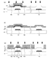
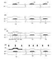
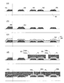
ここで、図2〜図4を参照して半導体装置100の製造方法を説明する。
Here, a method for manufacturing the
まず、図2(a)に示すように、絶縁基板101上に、ゲート電極122および下側電極142を形成する。ゲート電極122および下側電極142は、絶縁基板101の表面上に堆積した導電層を、フォトレジストマスク(図示せず)を利用して所定の形状にパターニングすることによって形成される。ゲート電極122はTFT領域に設けられており、下側電極142はコンタクト領域に設けられている。
First, as shown in FIG. 2A, the
次に、図2(b)に示すように、ゲート電極122および下側電極142を覆う絶縁層125を形成する。絶縁層125は、例えば厚さ250nmのSiO2から形成されている。
Next, as illustrated in FIG. 2B, an insulating
次に、図2(c)に示すように、絶縁層125の上に半導体層126を形成する。半導体層126は、絶縁層125の表面に堆積した半導体層を、フォトレジストマスク(図示せず)を利用して所定の形状にパターニングすることによって形成される。
Next, as illustrated in FIG. 2C, the
なお、半導体層126には、後述のドーピングにおいてドーパントの種類および/または濃度が隣接領域とは異なる5つの領域126s、126a、126c、126bおよび126dが設けられる。領域126s、126cおよび126dはそれぞれTFT120のソース領域、チャネル領域およびドレイン領域となり、領域126a、126bはそれぞれTFT120の第1、第2中間領域(LDD領域)となる。半導体層126のチャネル領域126cはゲート絶縁膜124を介してゲート電極122と対向している。
Note that the
次に、図2(d)に示すように、半導体層126に低濃度のドーパント(例えば、B)をドープする。なお、後述するように、半導体層126の領域126c以外の領域(すなわち、領域126s、126d、126aおよび126b)にはさらに別のドーパントがドープされるが、半導体層126のチャネル領域126cにはBのみがドープされる。このため、このようなドーピングはチャネルドーピングとも呼ばれる。
Next, as shown in FIG. 2D, the
次に、図3(e)に示すように、半導体層126上に、半導体層126の領域126a、126c、126bを覆うフォトレジストマスクPeを形成し、フォトレジストマスクPeを利用して半導体層126の領域126s、126dに高濃度のドーパント(例えば、P)をドープする。なお、本明細書において、このように、半導体層126のソース領域126s、ドレイン領域126dとなる領域に行うドーピングを第1ドーピングともいう。その後、フォトレジストマスクPeを剥離する。
Next, as illustrated in FIG. 3E, a photoresist mask Pe that covers the
次に、図3(f)に示すように、絶縁層125および半導体層126を覆う第1層間絶縁膜102を堆積する。第1層間絶縁膜102は、例えばSiNから形成されている。
Next, as shown in FIG. 3F, a first
次に、図3(g)に示すように、第1層間絶縁膜102上にフォトレジストマスクP1を形成する。フォトレジストマスクP1では、半導体層126の領域126a、126bの上方部分および下側電極142の上方部分が開口している。
Next, as illustrated in FIG. 3G, a photoresist mask P <b> 1 is formed on the first
このようなフォトレジストマスクP1を利用してエッチングを行う。以下の説明において、このようなエッチングを第1エッチングとも呼ぶ。第1エッチングは、例えばウエットエッチングで行われ、ウエットエッチングは、フッ酸(Hydrogen Fluoride:HF)または緩衝フッ酸(Buffered Hydrogen Fluoride:BHF)を用いて行われる。このエッチングにより、堆積された第1層間絶縁膜102のうち、半導体層126の領域126a、126bの上方部分および下側電極142の上方部分が除去される。
Etching is performed using such a photoresist mask P1. In the following description, such etching is also referred to as first etching. The first etching is performed by wet etching, for example, and the wet etching is performed using hydrofluoric acid (HF) or buffered hydrofluoric acid (BHF). By this etching, in the deposited first
さらに、フォトレジストマスクP1をマスクとして利用して半導体層126に比較的低量のドーパント(例えば、P)をドープする。これにより、半導体層126の領域126a、126bには低濃度のドーパントがドープされる。なお、本明細書において、このように、半導体層126の少なくとも第1、第2中間領域126a、126bとなる領域に行うドーピングを第2ドーピングともいう。
Further, the
なお、このドーピング後に加熱処理を行ってもよい。例えば、大気中または窒素ガスと水素ガスを含む雰囲気下で300〜400℃で加熱処理を行う。加熱処理により、水素化アニールおよび活性化アニールが行われ、半導体層126と第1層間絶縁膜102との界面が安定化するとともに、領域126sおよび領域126dの抵抗が低下する。
Note that heat treatment may be performed after the doping. For example, heat treatment is performed at 300 to 400 ° C. in the air or in an atmosphere containing nitrogen gas and hydrogen gas. By the heat treatment, hydrogenation annealing and activation annealing are performed, the interface between the
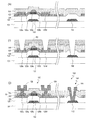
次に、図4(h)に示すように、フォトレジストマスクP1を剥離した後、絶縁層125、半導体層126および第1層間絶縁膜102を覆う第2層間絶縁膜104を堆積する。第2層間絶縁膜104は、例えばSiO2から形成されている。
Next, as shown in FIG. 4H, after removing the photoresist mask P1, a second
次に、図4(i)に示すように、堆積した第2層間絶縁膜104の上にフォトレジストマスクP2を形成する。フォトレジストマスクP2では、半導体層126の領域126s、126dの上方部分および下側電極142の上方部分が開口している。
Next, as shown in FIG. 4I, a photoresist mask P2 is formed on the deposited second
次に、フォトレジストマスクP2を利用してエッチングを行う。以下の説明において、このエッチングを第2エッチングとも呼ぶ。第2エッチングにより、TFT領域における第1層間絶縁膜102および第2層間絶縁膜104が除去されて半導体層126のソース領域126s、ドレイン領域126dの一部を露出するコンタクトホールが形成されるとともに、コンタクト領域における第2層間絶縁膜104および絶縁層125が除去されて下側電極142の一部を露出するコンタクトホールが形成される。
Next, etching is performed using the photoresist mask P2. In the following description, this etching is also referred to as second etching. By the second etching, the first
なお、エッチングとしてウェットエッチングを行ってもよいが、ウェットエッチングを行う場合、コンタクトホールが比較的大きくなってしまう。このため、エッチングとしてドライエッチングを行うことが好ましい。これにより、比較的小さいコンタクトホール(例えば、1.5μm〜2μm)を形成することができる。 Note that wet etching may be performed as etching, but when wet etching is performed, the contact hole becomes relatively large. For this reason, it is preferable to perform dry etching as etching. Thereby, a comparatively small contact hole (for example, 1.5 μm to 2 μm) can be formed.
ドライエッチングは、フッ素系ガスを用いた誘導結合プラズマ(Inductively Coupled Plasma:ICP)を用いて行われる。例えば、混合ガスとして、数mTorrのSF6およびArガスが用いられ、高周波出力は数kW程度である。 The dry etching is performed using inductively coupled plasma (ICP) using a fluorine-based gas. For example, SF 6 and Ar gas of several mTorr are used as the mixed gas, and the high frequency output is about several kW.
次に、図4(j)に示すように、フォトレジストマスクP2を剥離した後、半導体層126、下側電極142および第2層間絶縁膜104を覆う上側導電層を堆積し、上側導電層をパターニングすることによって、半導体層126のソース領域126sと電気的に接続されたソース電極128、半導体層126のドレイン領域126dと電気的に接続されたドレイン電極130、および、下側電極142と電気的に接続された上側電極144を形成する。以上のようにして半導体装置100が作製される。
Next, as shown in FIG. 4J, after removing the photoresist mask P2, an upper conductive layer covering the
このような半導体装置100は例えば液晶表示装置のアクティブマトリクス基板の作製に好適に用いられる。ここでは図示しないが、例えば、ソース電極128、ドレイン電極130、上側電極144および第2層間絶縁膜104上に別の透明層間絶縁膜をさらに堆積し、透明層間絶縁膜上に画素電極および配向膜を形成する。この画素電極は透明層間絶縁膜に設けられたコンタクトホールを介してドレイン電極130と電気的に接続されている。
Such a
なお、上述した説明では、フォトレジストマスクP1を利用して第1層間絶縁膜102のエッチングを行った後に、フォトレジストマスクP1を利用して領域126a、126bへのドーピングを行ったが、本発明はこれに限定されない。第1層間絶縁膜102が薄く、例えば、その厚さが100nm以下である場合、フォトレジストマスクP1を利用して第1層間絶縁膜102を介して半導体層126の領域126a、126bにドーピングを行った後に、フォトレジストマスクP1を利用して第1層間絶縁膜102のエッチングを行ってもよい。なお、第1層間絶縁膜102のエッチングおよび領域126a、126bへのドーピングの順番にかかわらず、第1層間絶縁膜102のエッチングは、半導体層126の領域126a、126bへのドーピングを行うためのフォトレジストマスクP1を利用して行われることにより、使用するフォトレジストマスクの数の増加を抑制できる。
In the above description, after the first
また、上述した説明では、領域126a、126bへのドーピングを行うためのマスクとしてフォトレジストマスクP1を利用したが、本発明はこれに限定されない。第1層間絶縁膜102が比較的厚く、例えば、その厚さが200nm以上である場合、第1層間絶縁膜102のエッチングに利用したフォトレジストマスクP1を剥離した後で、領域126a、126bにドーパントをドーピングするためのマスクとして第1層間絶縁膜102を利用してもよい。
In the above description, the photoresist mask P1 is used as a mask for doping the
また、上述した説明では、加熱処理は第1層間絶縁膜102を堆積した後であって第2層間絶縁膜104を堆積する前に行ったが、本発明はこれに限定されない。加熱処理は第2層間絶縁膜104を堆積した後に行ってもよい。
In the above description, the heat treatment is performed after the first
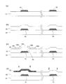
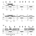
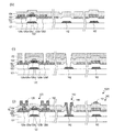
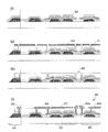
ここで、比較例の半導体装置と比較して本実施形態の半導体装置100の利点を説明する。まず、図5を参照して、比較例の半導体装置500を説明する。
Here, advantages of the
図5(a)に、半導体装置500の模式図を示す。半導体装置500では、TFT領域において第1層間絶縁膜502および第2層間絶縁膜504が積層しているだけでなく、コンタクト領域においても第1層間絶縁膜502および第2層間絶縁膜504が積層している。このように半導体装置500ではコンタクト領域においても第1層間絶縁膜502および第2層間絶縁膜504が積層している。
FIG. 5A shows a schematic diagram of the
ここで、比較例の半導体装置500において、上側導電層を堆積する前のエッチングに着目する。コンタクト領域において下側電極542が十分に露出するまでエッチングを行うと、図5(b)に示すように、半導体層526に孔が形成されてしまうことがある。この場合、その後にコンタクトホールに設けられるソース電極528およびドレイン電極530が半導体層526と十分に接触せず、接続不良が生じる。
Here, in the
あるいは、TFT領域において半導体層526に孔が形成しないようにエッチングを行うと、図5(c)に示すように、コンタクト部540において絶縁層525が十分に除去されずに残存してしまい、下側電極542が露出されない。この場合、その後にコンタクトホールに形成される上側電極544が下側電極542と接触しないことにより、接続不良が生じる。
Alternatively, if etching is performed so that no hole is formed in the
これに対して、半導体装置100では、コンタクト領域において絶縁層125上に第1層間絶縁膜102は設けられていないため、TFT領域において半導体層126に孔を形成することなく、かつ、コンタクト領域において下側電極142が露出するようにエッチングを行うことができる。また、TFT領域にコンタクトホールを形成するためのエッチングと、コンタクト領域にコンタクトホールを形成するためのエッチングとを同時に行うことができ、製造工程を簡略化するとともに製造時間を短縮できる。なお、第1層間絶縁膜102の材料および厚さは、エッチング工程において絶縁層125を除去するのに必要な時間と等しい時間で除去されるように調整されていることが好ましい。
On the other hand, in the
例えば、上述したように、絶縁層125がSiO2から形成され、第1層間絶縁膜102がSiNから形成され、第2層間絶縁膜104がSiO2から形成される場合、第2エッチングを行うと、TFT領域ではSiNから形成された第1層間絶縁膜102が除去され、コンタクト領域ではSiO2から形成された絶縁層125が除去される。このため、第1層間絶縁膜102および絶縁層125の厚さに応じて、エッチング条件(例えば、ドライエッチング条件)を調整してSiNとSiO2とのエッチングレート比を変化させてもよい。
For example, as described above, when the insulating
あるいは、絶縁層125がSiO2から形成され、第1層間絶縁膜102がSiO2から形成され、第2層間絶縁膜104がSiNから形成される場合、第1エッチングにおいて、コンタクト領域では、第1層間絶縁膜102の除去に続き、同じ材料から形成された絶縁層125が除去されることがある。このため、絶縁層125を第1層間絶縁膜104よりも厚くしてもよい。
Alternatively, when the insulating
なお、半導体装置を用いて液晶表示装置のアクティブマトリクス基板を作製する場合、下側導電層から形成された配線と上側導電層から形成された配線との間で容量結合を形成することがある。 Note that when an active matrix substrate of a liquid crystal display device is manufactured using a semiconductor device, capacitive coupling may be formed between a wiring formed from a lower conductive layer and a wiring formed from an upper conductive layer.
以下、図6を参照して半導体装置100Aの構成を説明する。半導体装置100Aは、TFT120およびコンタクト部140だけでなく容量結合部160を備えている点を除いて上述した半導体装置100と同様の構成を有している。したがって、冗長を避けるために重複する説明を省略する。
Hereinafter, the configuration of the
容量結合部160は、下側配線162と、上側配線164とを有しており、下側配線162および上側配線164の間には絶縁層125、第1層間絶縁膜102および第2層間絶縁膜104が設けられている。容量結合部160では、下側配線162と上側配線164との間で容量結合が形成される。なお、以下の説明において、容量結合部160の形成される領域およびその近傍を容量結合領域とも呼ぶ。
The
下側配線162はゲート電極122および下側電極142と同一工程で形成され、下側配線162は下側導電層から形成される。また、上側配線164はソース電極128、ドレイン電極130および上側電極144と同一工程で形成され、上側配線164は上側導電層から形成される。
The
なお、コンタクト領域では第1層間絶縁膜102が設けられていないのに対して、容量結合領域では絶縁層125および第2層間絶縁膜104だけでなく第1層間絶縁膜102が設けられている。このため、容量結合部160の静電容量は小さく、電荷変化量が小さくても容量結合部160の電圧変化量を大きくすることができる。このような容量結合部160は、例えばアクティブマトリクス基板の配線交差部として利用される。例えば、下側配線162は補助容量配線として用いられ、上側配線164はソース配線として用いられる。
The first
ここで、図7〜図9を参照して半導体装置100Aの製造方法を説明する。
Here, a method of manufacturing the
まず、図7(a)に示すように、絶縁基板101上に、ゲート電極122、下側電極142および下側配線162を形成する。
First, as shown in FIG. 7A, the
次に、図7(b)に示すように、ゲート電極122、下側電極142および下側配線162を覆う絶縁層125を形成する。
Next, as illustrated in FIG. 7B, an insulating
次に、図7(c)に示すように、絶縁層125の上に半導体層126を形成する。半導体層126は、絶縁層125の表面に堆積した半導体層を、フォトレジストマスク(図示せず)を利用して所定の形状にパターニングすることによって形成される。
Next, as illustrated in FIG. 7C, the
次に、図7(d)に示すように、低量のドーパント(例えば、B)を注入する。これにより、半導体層126に低濃度のドーパントがドープされる。
Next, as shown in FIG. 7D, a low amount of dopant (for example, B) is implanted. Thereby, the
次に、図8(e)に示すように、半導体層126上に、半導体層126の領域126a、126c、126bを覆うフォトレジストマスクPeを形成し、フォトレジストマスクPeを利用して半導体層126の領域126s、126dに高濃度のドーパント(例えば、P)をドープする。
Next, as shown in FIG. 8E, a photoresist mask Pe covering the
次に、図8(f)に示すように、絶縁層125および半導体層126を覆う第1層間絶縁膜102を堆積する。第1層間絶縁膜102は例えばSiNから形成されている。
Next, as shown in FIG. 8F, a first
次に、図8(g)に示すように、第1層間絶縁膜102上にフォトレジストマスクP1を形成する。フォトレジストマスクP1では、半導体層126の領域126a、126bの上方部分および下側電極142の上方部分が開口している。
Next, as illustrated in FIG. 8G, a photoresist mask P <b> 1 is formed on the first
第1層間絶縁膜102のエッチングはこのようなフォトレジストマスクP1を利用して行われる。エッチングにより、第1層間絶縁膜102のうち、半導体層126の領域126a、126bの上方部分および下側電極142の上方部分が除去される。さらに、フォトレジストマスクP1をマスクとして利用して比較的低量のドーパント(例えば、P)をドープすることにより、半導体層126の領域126a、126bにドーピングを行う。
Etching of the first
なお、第1層間絶縁膜102にドーピングを行った後に、加熱処理を行ってもよい。加熱処理により、水素化アニールおよび活性化アニールが行われる。これにより、半導体層126と第1層間絶縁膜102との界面が安定化するとともに、ソース領域126sおよびドレイン領域126dの抵抗が低下する。
Note that heat treatment may be performed after the first
次に、図9(h)に示すように、フォトレジストマスクP1を剥離した後、絶縁層125、半導体層126および第1層間絶縁膜102を覆う第2層間絶縁膜104を堆積する。第2層間絶縁膜104は、例えばSiO2から形成されている。
Next, as shown in FIG. 9H, after the photoresist mask P1 is peeled off, a second
次に、図9(i)に示すように、第2層間絶縁膜104の上にフォトレジストマスクP2を形成する。フォトレジストマスクP2では、半導体層126の領域126s、126dの上方部分および下側電極142の上方部分が開口している。
Next, as illustrated in FIG. 9I, a photoresist mask P <b> 2 is formed on the second
次に、フォトレジストマスクP2を利用して絶縁層125、第1層間絶縁膜102および第2層間絶縁膜104のエッチングを行う。このエッチングにより、TFT領域において第1層間絶縁膜102および第2層間絶縁膜104の一部が除去されて半導体層126のソース領域126s、ドレイン領域126dを露出するコンタクトホールが形成され、コンタクト領域において第2層間絶縁膜104および絶縁層125の一部が除去されて下側電極142を露出するコンタクトホールが形成される。
Next, the insulating
次に、図9(j)に示すように、フォトレジストマスクP2を剥離した後、半導体層126および第2層間絶縁膜104を覆う上側導電層を堆積する。上側導電層をパターニングすることによって、半導体層126のソース領域126sと電気的に接続されたソース電極128、半導体層126のドレイン領域126dと電気的に接続されたドレイン電極130、および、下側電極142と電気的に接続された上側電極144だけでなく、下側配線162と絶縁層125、第1層間絶縁膜102および第2層間絶縁膜104を介して対向する上側配線164を形成する。以上のようにして半導体装置100Aが形成される。
Next, as shown in FIG. 9J, after the photoresist mask P2 is peeled off, an upper conductive layer that covers the
なお、上述した説明では、半導体層126のチャネル領域126cとソース領域126s、ドレイン領域126dとの間に第1、第2中間領域126a、126bが設けられていたが、本発明はこれに限定されない。半導体層126に第1、第2中間領域126a、126bが設けられなくてもよい。
In the above description, the first and second
図10を参照して、半導体装置100Bの構成を説明する。半導体層126Bは第1、第2中間領域126a、126bを有していない点を除いて図1に示した半導体装置100の半導体層126と同様の構成を有しており、冗長を避けるために、重複する説明を省略する。
The configuration of the
半導体層126Bにおいて、チャネル領域126cはソース領域126sおよびドレイン領域126dのそれぞれと隣接している。また、半導体層126Bにはソース電極128およびドレイン電極130のためのコンタクトホールが設けられている領域を除いて第1層間絶縁膜102が半導体層126Bを覆っている。LDD領域を有しない半導体層126Bを含むTFT120Bは、例えば、アクティブマトリクス基板の周辺回路部に好適に用いられる。具体的には、TFT120Bは、高速動作が必要なシフトレジスタ等に好適に用いられる。なお、周辺回路部のNチャネルトランジスタとしては、LDD領域を有さないTFT120BだけでなくLDD領域を有する上述したTFT120が用いられる。特に、動作電圧が高い場合、LDD領域を有するTFT120を用いることが好適である。なお、Pチャネルトランジスタの場合、信頼性の問題が生じないので、LDD領域を設ける必要はない。
In the semiconductor layer 126B, the
なお、上述した説明では、第1層間絶縁膜102のうちの下側電極142の上方部分を除去するためのマスクとして、第1、第2中間領域126a、126bにドーピングを行うためのフォトレジストマスクP1を利用したが、本発明はこれに限定されない。また、上述した説明では、第1、第2中間領域126a、126bへのドーピングに利用されるフォトレジストマスクP1は半導体層126のチャネル領域126c上方を覆っており、その結果、半導体層126のチャネル領域126上には第1層間絶縁膜102が設けられていたが、本発明はこれに限定されない。
In the above description, a photoresist mask for doping the first and second
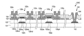
以下、図11を参照して、半導体装置100Cの構成を説明する。半導体装置100CにはNチャネルTFT120n、PチャネルTFT120p、および、コンタクト部140が設けられている。ここでは、TFT120nは第1、第2中間領域(LDD領域)126na、126nbを有しており、上述したように、このようなTFT120nは画素領域のTFTとして好適に用いられる。
Hereinafter, the configuration of the
半導体層126nはLDD領域を有しているのに対して、半導体層126pはLDD領域を有していない。このため、TFT120nの半導体層126nでは、チャネル領域126ncとソース領域126nsまたはドレイン領域126ndとの間に第1中間領域126naおよび第2中間領域126nbがそれぞれ設けられているが、TFT120pの半導体層126pでは、ソース領域126psおよびドレイン領域126pdのそれぞれはチャネル領域126pcと隣接している。なお、半導体層126pにおけるチャネル領域126pcの上には第1層間絶縁膜102が設けられているのに対して、半導体層126nにおけるチャネル領域126ncの上には第1層間絶縁膜102は設けられていない。
The
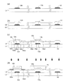
ここで、図12〜図14を参照して半導体装置100Cの製造方法を説明する。
Here, a method of manufacturing the
まず、図12(a)に示すように、絶縁基板101上に下側導電層を堆積し、この下側導電層を所定の形状のフォトレジストマスク(図示せず)を利用してパターニングすることにより、ゲート電極122n、122pおよび下側電極142を形成する。
First, as shown in FIG. 12A, a lower conductive layer is deposited on an insulating
次に、図12(b)に示すように、ゲート電極122n、122pおよび下側電極142を覆う絶縁層125を形成する。
Next, as shown in FIG. 12B, an insulating
次に、図12(c)に示すように、絶縁層125上に半導体層126n、126pを形成する。半導体層126n、126pは絶縁層125上に半導体材料を堆積した後で所定の形状のフォトレジストマスク(図示せず)を利用してエッチングを行うことによって形成される。
Next, as illustrated in FIG. 12C, semiconductor layers 126 n and 126 p are formed over the insulating
なお、半導体層126nには、後述のドーピングにおいてドーパントの種類および/または濃度が隣接領域とは異なる5つの領域126ns、126na、126nc、126nbおよび126ndが設けられる。領域126ns、126ncおよび126ndはそれぞれTFT120nのソース領域、チャネル領域およびドレイン領域となり、領域126na、126nbはそれぞれTFT120nの第1、第2中間領域(LDD領域)となる。半導体層126nのチャネル領域126ncはゲート絶縁膜124nを介してゲート電極122nと対向している。
Note that the
また、半導体層126pには、後述のドーピングにおいてドーパントの種類および/または濃度が隣接領域とは異なる3つの領域126ps、126pcおよび126pdが設けられる。領域126ps、126pcおよび126pdはそれぞれTFT120pのソース領域、チャネル領域およびドレイン領域となる。半導体層126pのチャネル領域126pcはゲート絶縁膜124pを介してゲート電極122pと対向している。
In addition, the
次に、図12(d)に示すように、フォトレジストマスクPdを形成する。フォトレジストマスクPdは半導体層126nの領域126na、126nc、126ndと半導体層126pの全体を覆っている。このようなフォトレジストマスクPdを利用して半導体層126nの領域126nsおよび126ndに多量のドーパント(例えば、P)をドープする。このようにして、半導体層126nの領域126ns、126ndには高濃度のドーパントがドーピングされる。
Next, as shown in FIG. 12D, a photoresist mask Pd is formed. The photoresist mask Pd covers the regions 126na, 126nc, 126nd of the
次に、図13(e)に示すように、フォトレジストマスクPeを形成する。フォトレジストマスクPeは半導体層126nの領域126nc、および、半導体層126pの領域126pcを覆っているが、フォトレジストマスクPeはフォトレジストマスクPdよりも小さい。半導体層126nでは高濃度のドーパントをドープされていない領域126na、126nbが露出されており、半導体層126pでは領域126ps、126pdが露出されている。フォトレジストマスクPeの形成は、下側導電層をマスクとして利用した裏面露光によって行われる。
Next, as shown in FIG. 13E, a photoresist mask Pe is formed. The photoresist mask Pe covers the region 126nc of the
このようなフォトレジストマスクPeを利用して半導体層126nの領域126s、126na、126nbおよび126ndに低量のドーパント(例えば、P)をドープする。このドーピングにより、半導体層126nの領域126na、126nbに低濃度のドーパントがドーピングされる。また、このとき、半導体層126pの領域126ps、126pdに低濃度のドーパントがドーピングされる。なお、半導体層126nの領域126ns、126ndにはすでに高濃度のドーパントがドーピングされている。また、後述するように、半導体層126pの領域126ps、126pdには高濃度のドーパントがドーピングされる。
Using such a photoresist mask Pe, the
次に、図13(f)に示すように、フォトレジストマスクPfを形成する。フォトレジストマスクPfは半導体層126nの全体と半導体層126pの領域126pcを覆っている。このようなフォトレジストマスクPfを利用して半導体層126pの領域126ps、126pdに高濃度のドーパント(例えば、N)をドーピングする。このとき、半導体層126pにおいて、高濃度のドーパントがドーピングされる領域は先にドーピングが行われた領域の境界よりも内側にまで位置している。その後、フォトレジストマスクPfを剥離する。
Next, as shown in FIG. 13F, a photoresist mask Pf is formed. The photoresist mask Pf covers the
次に、図13(g)に示すように、絶縁層125および半導体層126n、126pを覆う第1層間絶縁膜102を堆積する。なお、第1層間絶縁膜102を堆積した後に加熱処理を行ってもよい。
Next, as shown in FIG. 13G, a first
その後、第1層間絶縁膜102を介して半導体層126n、半導体層126pに低量のドーパント(例えば、B)をドーピングする。このドーピングはフォトレジストマスクを設けることなく行われる。これにより、半導体層126n、126pのチャネル領域126nc、126pcにもドーパントがドーピングされる。このため、このようなドーピングはチャネルドーピングとも呼ばれる。以下の説明において、このドーピングを1回目のチャネルドーピングと呼ぶことがある。なお、一般に、半導体層126nのチャネル領域126ncのドーズ量は半導体層126pのチャネル領域126pcよりも多いことが好ましい。このため、半導体層126nのチャネル領域126ncのためにさらなるチャネルドーピングが行われる。
Thereafter, a low amount of dopant (for example, B) is doped into the
次に、図14(h)に示すように、半導体層126nの領域126ncおよびコンタクト領域が開口されたフォトレジストマスクP1を形成する。その後、フォトレジストマスクP1を利用して第1層間絶縁膜102のエッチングを行うことによって、半導体層126nの領域126ncおよびコンタクト領域の絶縁層125が露出される。その後、フォトレジストマスクP1を利用して半導体層126nのチャネル領域126ncに低量のドーパント(例えば、B)をドーピングする。このドーピングは2回目のチャネルドーピングとも呼ばれる。なお、上述したように、半導体層126nの領域126nc以外の領域(すなわち、領域126ns、126nd、126naおよび126nb)にはすでに別のドーパントがドープされているが、半導体層126nのチャネル領域126ncにはBのみがドープされる。
Next, as shown in FIG. 14H, a photoresist mask P1 in which the region 126nc of the
なお、上述した説明では、1回目のチャネルドーピングは第1層間絶縁膜102を形成した後で、第1層間絶縁膜102を介して行われたが、これに限定されない。例えば、半導体層126n、126pを形成した後、半導体層126nのソース領域126ns、ドレイン領域126ndへのドーピングを行う前に1回目のチャネルドーピングを行ってもよい。
In the above description, the first channel doping is performed through the first
次に、図14(i)に示すように、フォトレジストマスクP1を剥離し、絶縁層125、半導体層126および第1層間絶縁膜102を覆う第2層間絶縁膜104を堆積する。
Next, as shown in FIG. 14I, the photoresist mask P1 is peeled off, and a second
次に、図14(j)に示すように、第2層間絶縁膜104の上にフォトレジストマスクP2を形成する。フォトレジストマスクP2では、半導体層126nのソース領域126ns、ドレイン領域126nd、半導体層126pのソース領域126ps、ドレイン領域126pdの上方部分およびコンタクト領域が開口している。
Next, as illustrated in FIG. 14J, a photoresist mask P <b> 2 is formed on the second
その後、フォトレジストマスクP2を利用してエッチングを行う。このエッチングにより、TFT領域において第1層間絶縁膜102および第2層間絶縁膜104が除去されて半導体層126nのソース領域126ns、ドレイン領域126nd、半導体層126pのソース領域126psを露出するコンタクトホールが形成され、コンタクト領域において第2層間絶縁膜104および絶縁層125が除去されて下側電極142を露出するコンタクトホールが形成される。
Thereafter, etching is performed using the photoresist mask P2. By this etching, the first
次に、図14(k)に示すように、フォトレジストマスクP2を剥離し、半導体層126および第2層間絶縁膜104を覆う上側導電層を堆積し、上側導電層を所定の形状のフォトレジストマスク(図示せず)を利用してエッチングすることにより、ソース領域126ns、126ps、ドレイン領域126nd、126pdと電気的に接続されたソース電極128n、128pおよびドレイン電極130n、130pと、下側電極142と電気的に接続された上側電極144とを形成する。以上のようにして半導体装置100Cが形成される。なお、半導体装置100Cに図6に示した容量結合部160がさらに設けられてもよい。
Next, as shown in FIG. 14K, the photoresist mask P2 is peeled off, an upper conductive layer covering the
なお、上述した説明では、フォトレジストマスクP1を利用して第1層間絶縁膜102のエッチングを行った後に、フォトレジストマスクP1を利用して半導体層126nへのチャネルドーピングを行ったが、本発明はこれに限定されない。第1層間絶縁膜102が薄く、例えば、その厚さが100nm以下である場合、フォトレジストマスクP1を利用して第1層間絶縁膜102を介して半導体層126nにチャネルドーピングを行った後に、フォトレジストマスクP1を利用して第1層間絶縁膜102のエッチングを行ってもよい。なお、第1層間絶縁膜102のエッチングおよびチャネルドーピングの順番にかかわらず、第1層間絶縁膜102のエッチングはチャネルドーピングを行うためのフォトレジストマスクP1を利用して行われることにより、使用するフォトレジストマスクの数の増加を抑制できる。
In the above description, the first
また、上述した説明では、チャネルドーピングを行うためのマスクとしてフォトレジストマスクP1を利用したが、本発明はこれに限定されない。第1層間絶縁膜102が比較的厚く、例えば、その厚さが200nm以上である場合、第1層間絶縁膜102のエッチングに利用したフォトレジストマスクP1を剥離した後で、チャネルドーピングするためのマスクとして第1層間絶縁膜102を利用してもよい。
In the above description, the photoresist mask P1 is used as a mask for channel doping, but the present invention is not limited to this. When the first
本発明による半導体装置は、液晶表示装置のアクティブマトリクス基板の作製に好適に用いられる。また、このような液晶表示装置は携帯電話、デジタルカメラ等に好適に用いられる。 The semiconductor device according to the present invention is suitably used for manufacturing an active matrix substrate of a liquid crystal display device. Such a liquid crystal display device is suitably used for a mobile phone, a digital camera, and the like.
100 半導体装置
102 第1層間絶縁膜
104 第2層間絶縁膜
120 TFT
140 コンタクト部
160 容量結合部
DESCRIPTION OF
140
Claims (13)
前記ゲート電極と同じ材料から形成された下側電極と、
前記ゲート電極および前記下側電極を覆う絶縁層と、
ソース領域、チャネル領域およびドレイン領域を有する半導体層であって、前記チャネル領域が前記絶縁層を介して前記ゲート電極と対向する、半導体層と、
前記絶縁層の一部および前記半導体層を覆う第1層間絶縁膜であって、前記絶縁層のうちの前記下側電極上の領域を覆わない第1層間絶縁膜と、
前記絶縁層および前記第1層間絶縁膜を覆う第2層間絶縁膜と、
前記第1層間絶縁膜および前記第2層間絶縁膜に設けられたコンタクトホールを介して前記半導体層の前記ソース領域と電気的に接続されたソース電極と、
前記第1層間絶縁膜および前記第2層間絶縁膜に設けられたコンタクトホールを介して前記半導体層の前記ドレイン領域と電気的に接続されたドレイン電極と、
前記ソース電極および前記ドレイン電極と同じ材料から形成された上側電極であって、前記絶縁層および前記第2層間絶縁膜に設けられたコンタクトホールを介して前記下側電極と電気的に接続された上側電極と
を備える、半導体装置。 A gate electrode;
A lower electrode formed of the same material as the gate electrode;
An insulating layer covering the gate electrode and the lower electrode;
A semiconductor layer having a source region, a channel region, and a drain region, wherein the channel region is opposed to the gate electrode through the insulating layer;
A first interlayer insulating film covering a part of the insulating layer and the semiconductor layer, the first interlayer insulating film not covering a region on the lower electrode of the insulating layer;
A second interlayer insulating film covering the insulating layer and the first interlayer insulating film;
A source electrode electrically connected to the source region of the semiconductor layer through a contact hole provided in the first interlayer insulating film and the second interlayer insulating film;
A drain electrode electrically connected to the drain region of the semiconductor layer through a contact hole provided in the first interlayer insulating film and the second interlayer insulating film;
An upper electrode made of the same material as the source electrode and the drain electrode, and electrically connected to the lower electrode through a contact hole provided in the insulating layer and the second interlayer insulating film A semiconductor device comprising an upper electrode.
前記ソース電極、前記ドレイン電極および前記上側電極と同じ材料から形成された上側配線であって、前記絶縁層、前記第1層間絶縁膜および前記第2層間絶縁膜を介して前記下側配線と対向する上側配線と
をさらに備える、請求項1に記載の半導体装置。 A lower wiring formed of the same material as the gate electrode and the lower electrode;
An upper wiring formed of the same material as the source electrode, the drain electrode, and the upper electrode, and opposed to the lower wiring through the insulating layer, the first interlayer insulating film, and the second interlayer insulating film The semiconductor device according to claim 1, further comprising an upper wiring.
前記半導体層の前記ソース領域および前記ドレイン領域のそれぞれにはドーパントがドープされており、
前記第1中間領域には、前記ソース領域よりも低濃度のドーパントがドープされており、前記第2中間領域には、前記ドレイン領域よりも低濃度のドーパントがドープされている、請求項1または2に記載の半導体装置。 The semiconductor layer further includes a first intermediate region located between the source region and the channel region, and a second intermediate region located between the channel region and the drain region,
Each of the source region and the drain region of the semiconductor layer is doped with a dopant,
The first intermediate region is doped with a lower concentration dopant than the source region, and the second intermediate region is doped with a lower concentration dopant than the drain region. 2. The semiconductor device according to 2.
前記第1中間領域および前記第2中間領域のそれぞれは、前記第2層間絶縁膜で覆われている、請求項3に記載の半導体装置。 Each of the source region and the drain region of the semiconductor layer is covered with the first interlayer insulating film,
4. The semiconductor device according to claim 3, wherein each of the first intermediate region and the second intermediate region is covered with the second interlayer insulating film.
前記ゲート電極および前記下側電極を覆う絶縁層を形成する工程と、
ソース領域、チャネル領域およびドレイン領域を有する半導体層を形成する工程であって、前記チャネル領域は前記絶縁層を介して前記ゲート電極と対向する、工程と、
前記絶縁層および前記半導体層を覆う第1層間絶縁膜を堆積する工程と、
前記第1層間絶縁膜のうち少なくとも前記下側電極と対向する部分を除去するように前記第1層間絶縁膜のエッチングを行う工程と、
前記絶縁層および前記第1層間絶縁膜を覆う第2層間絶縁膜を堆積する工程と、
前記半導体層のうちの前記ソース領域および前記ドレイン領域のそれぞれの少なくとも一部が露出するように前記第1層間絶縁膜および前記第2層間絶縁膜にコンタクトホールを形成するとともに、前記下側電極が露出するように前記絶縁層および前記第2層間絶縁膜にコンタクトホールを形成する工程と、
前記コンタクトホールを形成した後に上側導電層を堆積し、前記上側導電層から、前記半導体層の前記ソース領域および前記ドレイン領域とそれぞれ電気的に接続されたソース電極およびドレイン電極を形成するとともに前記下側電極と電気的に接続された上側電極を形成する工程と
を包含する、半導体装置の製造方法。 Depositing a lower conductive layer and forming a gate electrode and a lower electrode from the lower conductive layer;
Forming an insulating layer covering the gate electrode and the lower electrode;
Forming a semiconductor layer having a source region, a channel region, and a drain region, the channel region facing the gate electrode through the insulating layer;
Depositing a first interlayer insulating film covering the insulating layer and the semiconductor layer;
Etching the first interlayer insulating film so as to remove at least a portion of the first interlayer insulating film facing the lower electrode;
Depositing a second interlayer insulating film covering the insulating layer and the first interlayer insulating film;
A contact hole is formed in the first interlayer insulating film and the second interlayer insulating film so that at least a part of each of the source region and the drain region of the semiconductor layer is exposed, and the lower electrode is Forming a contact hole in the insulating layer and the second interlayer insulating film so as to be exposed;
After forming the contact hole, an upper conductive layer is deposited to form a source electrode and a drain electrode electrically connected to the source region and the drain region of the semiconductor layer from the upper conductive layer, respectively, and Forming an upper electrode electrically connected to the side electrode.
前記上側導電層から、前記絶縁層、前記第1層間絶縁膜および前記第2層間絶縁膜を介して前記下側配線と対向する上側配線を形成する工程と
をさらに包含する、請求項7または8に記載の半導体装置の製造方法。 Forming a lower wiring from the lower conductive layer;
The method further comprises: forming an upper wiring facing the lower wiring from the upper conductive layer via the insulating layer, the first interlayer insulating film, and the second interlayer insulating film. The manufacturing method of the semiconductor device as described in any one of.
前記半導体層の前記チャネル領域、前記第1中間領域および前記第2中間領域と重なるとともに前記半導体層の前記ソース領域および前記ドレイン領域と重ならないフォトレジストマスクを利用して第1ドーピングを行う工程と、
前記半導体層のうちの少なくとも前記チャネル領域と重なるとともに前記半導体層のうちの少なくとも前記第1中間領域および前記第2中間領域と重ならないフォトレジストマスクを利用して第2ドーピングを行う工程と
をさらに包含する、請求項7から9のいずれかに記載の半導体装置の製造方法。 The semiconductor layer further includes a first intermediate region provided between the source region and the channel region, and a second intermediate region provided between the channel region and the drain region. ,
Performing a first doping using a photoresist mask that overlaps the channel region, the first intermediate region, and the second intermediate region of the semiconductor layer and does not overlap the source region and the drain region of the semiconductor layer; ,
Performing a second doping using a photoresist mask that overlaps at least the channel region of the semiconductor layer and does not overlap at least the first intermediate region and the second intermediate region of the semiconductor layer; The manufacturing method of the semiconductor device in any one of Claim 7 to 9 included.
前記第1層間絶縁膜のエッチングは、前記チャネルドーピングを行う前または前記チャネルドーピングを行った後に、前記チャネルドーピングのフォトレジストマスクを利用して行われる、請求項11または12に記載の半導体装置の製造方法。 Further comprising channel doping using a photoresist mask that does not cover at least the channel region of the semiconductor layer;
The semiconductor device according to claim 11, wherein the etching of the first interlayer insulating film is performed using the photoresist mask of the channel doping before the channel doping or after the channel doping. Production method.
Priority Applications (1)
| Application Number | Priority Date | Filing Date | Title |
|---|---|---|---|
| JP2008317583A JP2010141211A (en) | 2008-12-12 | 2008-12-12 | Semiconductor device |
Applications Claiming Priority (1)
| Application Number | Priority Date | Filing Date | Title |
|---|---|---|---|
| JP2008317583A JP2010141211A (en) | 2008-12-12 | 2008-12-12 | Semiconductor device |
Publications (1)
| Publication Number | Publication Date |
|---|---|
| JP2010141211A true JP2010141211A (en) | 2010-06-24 |
Family
ID=42351065
Family Applications (1)
| Application Number | Title | Priority Date | Filing Date |
|---|---|---|---|
| JP2008317583A Pending JP2010141211A (en) | 2008-12-12 | 2008-12-12 | Semiconductor device |
Country Status (1)
| Country | Link |
|---|---|
| JP (1) | JP2010141211A (en) |
Cited By (1)
| Publication number | Priority date | Publication date | Assignee | Title |
|---|---|---|---|---|
| JP2021076851A (en) * | 2011-11-11 | 2021-05-20 | 株式会社半導体エネルギー研究所 | Display device |
-
2008
- 2008-12-12 JP JP2008317583A patent/JP2010141211A/en active Pending
Cited By (2)
| Publication number | Priority date | Publication date | Assignee | Title |
|---|---|---|---|---|
| JP2021076851A (en) * | 2011-11-11 | 2021-05-20 | 株式会社半導体エネルギー研究所 | Display device |
| JP7339971B2 (en) | 2011-11-11 | 2023-09-06 | 株式会社半導体エネルギー研究所 | Display device |
Similar Documents
| Publication | Publication Date | Title |
|---|---|---|
| TWI401802B (en) | Thin film transistor plate and method of fabricating the same | |
| US8357570B2 (en) | Pixel structure and method for fabricating the same | |
| CN110071176B (en) | Top gate self-aligned metal oxide semiconductor TFT, manufacturing method thereof and display panel | |
| US7998803B2 (en) | Pixel structure and method for manufacturing the same | |
| US7755708B2 (en) | Pixel structure for flat panel display | |
| JP2006163389A (en) | Thin film transistor liquid crystal display, laminated storage capacitor, and method of fabricating the same | |
| US7842954B2 (en) | Active matrix array structure | |
| JP6437574B2 (en) | THIN FILM TRANSISTOR AND METHOD FOR MANUFACTURING SAME, ARRAY SUBSTRATE, AND DISPLAY DEVICE | |
| TW200301565A (en) | Thin film transistor substrate and method of manufacturing the same | |
| JP2008028399A (en) | Display with thin film transistor device having different electrical characteristics in pixel and driving regions, and method for fabricating the same | |
| JP2011166120A (en) | Thin-film transistor and method for forming the same | |
| WO2020228499A1 (en) | Transistor device and manufacturing method therefor, display substrate and display apparatus | |
| TW200819888A (en) | TFT substrate and manufacturing method, and display device with the same | |
| WO2015143818A1 (en) | Array substrate and method for fabrication and display device thereof | |
| US8008135B2 (en) | Method for manufacturing pixel structure | |
| JP2004140355A (en) | Pixel structure and its manufacturing method | |
| CN110299322B (en) | Display substrate, manufacturing method thereof and display device | |
| WO2015100859A1 (en) | Array substrate and method for manufacturing same, and display device | |
| US20090085039A1 (en) | Image display system and fabrication method thereof | |
| WO2018061851A1 (en) | Active matrix substrate and method for manufacturing same | |
| JP2007033786A (en) | Display device | |
| JP2010141211A (en) | Semiconductor device | |
| CN112309970B (en) | Manufacturing method of array substrate and array substrate | |
| US6703266B1 (en) | Method for fabricating thin film transistor array and driving circuit | |
| JP4441299B2 (en) | Manufacturing method of display device |