JP2010141007A - Semiconductor device, method of manufacturing the same, and electrostatic discharge protective element - Google Patents
Semiconductor device, method of manufacturing the same, and electrostatic discharge protective element Download PDFInfo
- Publication number
- JP2010141007A JP2010141007A JP2008314307A JP2008314307A JP2010141007A JP 2010141007 A JP2010141007 A JP 2010141007A JP 2008314307 A JP2008314307 A JP 2008314307A JP 2008314307 A JP2008314307 A JP 2008314307A JP 2010141007 A JP2010141007 A JP 2010141007A
- Authority
- JP
- Japan
- Prior art keywords
- semiconductor region
- region
- semiconductor
- insulating film
- conductivity type
- Prior art date
- Legal status (The legal status is an assumption and is not a legal conclusion. Google has not performed a legal analysis and makes no representation as to the accuracy of the status listed.)
- Pending
Links
Images


Landscapes
- Semiconductor Integrated Circuits (AREA)
- Metal-Oxide And Bipolar Metal-Oxide Semiconductor Integrated Circuits (AREA)
- Insulated Gate Type Field-Effect Transistor (AREA)
Abstract
【課題】製造効率を向上すると共に、内部回路の保護を的確に行うことが容易に可能な半導体装置、半導体装置の製造方法、静電放電保護素子を提供する。
【解決手段】半導体基板20に第1導電型の第1半導体領域21が形成され、その両側に第2導電型の第2及び第3半導体領域(22,23)が形成され、第1半導体領域の上方に絶縁膜を介してゲート電極32が形成され、第1半導体領域と第3半導体領域の接合面をまたいでそれらにかかるように第1導電型の第4半導体領域30が形成され、第2及び第3半導体領域にソース領域26とドレイン領域28が形成され、ゲート電極及びソース領域が接地され、内部回路に接続された入力パッド40がドレイン領域に接続され、入力パッドにサージ電圧が入力された際にドレイン領域と第4半導体領域との間でツェナー降伏が生じて寄生バイポーラトランジスタがオン状態となり、サージ電圧を放電する。
【選択図】図3Provided are a semiconductor device, a semiconductor device manufacturing method, and an electrostatic discharge protection element capable of improving manufacturing efficiency and easily protecting an internal circuit accurately.
A first semiconductor region of a first conductivity type is formed in a semiconductor substrate, and second and third semiconductor regions of a second conductivity type are formed on both sides of the first semiconductor region. A gate electrode 32 is formed above the first semiconductor region 30 via an insulating film, and a fourth semiconductor region 30 of the first conductivity type is formed so as to cross over the junction surface of the first semiconductor region and the third semiconductor region, and The source region 26 and the drain region 28 are formed in the second and third semiconductor regions, the gate electrode and the source region are grounded, the input pad 40 connected to the internal circuit is connected to the drain region, and a surge voltage is input to the input pad. In this case, a Zener breakdown occurs between the drain region and the fourth semiconductor region, and the parasitic bipolar transistor is turned on to discharge a surge voltage.
[Selection] Figure 3
Description
本発明は、半導体装置、半導体装置の製造方法、静電放電保護素子に関する。特に、本発明は、サージから内部回路を保護する静電放電保護素子と、この静電放電保護素子を含む半導体装置、および、その製造方法に関する。 The present invention relates to a semiconductor device, a method for manufacturing a semiconductor device, and an electrostatic discharge protection element. In particular, the present invention relates to an electrostatic discharge protection element that protects an internal circuit from a surge, a semiconductor device including the electrostatic discharge protection element, and a manufacturing method thereof.
静電放電(ESD:Electro Static Discharge)は、半導体装置の取り扱い時に生じ、人体、材料、装置等に起因する。このESDによる放電は電流ピーク値が数アンペアに及び、サージ電流が半導体装置の内部回路を破壊する。ICの微細化、高集積化に伴い、ESD耐性を向上させることが必要であり、内部回路が破壊されることを防止するために、ESD保護素子が設けられている。ESD保護素子としては、寄生バイポーラ動作を利用したMOS FET型が、知られている。このMOS FET型のESD保護素子は、たとえば、GG(Grounded Gate)MOSであり、スナップバック現象を利用している。 Electrostatic discharge (ESD) occurs when a semiconductor device is handled, and is caused by a human body, material, device, or the like. The discharge due to ESD has a current peak value of several amperes, and a surge current destroys an internal circuit of the semiconductor device. With the miniaturization and high integration of ICs, it is necessary to improve the ESD resistance, and an ESD protection element is provided to prevent the internal circuit from being destroyed. As an ESD protection element, a MOS FET type using a parasitic bipolar operation is known. This MOS FET type ESD protection element is, for example, a GG (Grounded Gate) MOS and utilizes a snapback phenomenon.
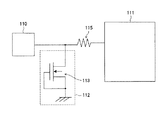
図10は従来例に係る保護回路であるGGMOSを有する回路の回路図である。例えば、パッド電極110及びそれに接続する内部回路111に対して保護素子112が設けられている構成である。保護素子112はGGMOS113を有する。保護素子112との接続点と内部回路111の間に抵抗素子115が設けられている。
FIG. 10 is a circuit diagram of a circuit having GGMOS as a protection circuit according to a conventional example. For example, the
図11(a)は図10に係る保護回路であるGGMOSの断面図であり、図11(b)は対応する平面図である。例えば、N型の半導体基板120にP型ウェル121が設けられており、活性領域を除く半導体基板120の表層にSTI(Shallow Trench Isolation)型の素子分離絶縁膜122(I)が形成されている。P型ウェル121の上層にゲート絶縁膜123を介してゲート電極124(G)が形成されている。ゲート電極124の両側部におけるP型ウェル121の表層部分にN型のソース領域125(NSD1)及びドレイン領域126(NSD2)が形成されている。ゲート電極124(G)、ソース領域125(NSD1)及びドレイン領域126(NSD2)の表層にはシリサイドが形成されていてもよい。
FIG. 11A is a sectional view of a GGMOS that is a protection circuit according to FIG. 10, and FIG. 11B is a corresponding plan view. For example, a P-
上記のGGMOSにおいては、入力パッドPADにドレイン領域126(NSD2)が接続されており、ソース領域125(NSD1)とゲート電極124(G)とのそれぞれが、グランドに接続されている。サージが入力パッドPADに入力された場合には、内部回路にサージが入力される前に、GGMOSにおいて、ドレイン電圧が上昇して電流が流れる。ここでは、GGMOSのソース領域とチャネル形成領域とドレイン領域とで構成される寄生バイポーラトランジスタが、オン状態になり、この寄生バイポーラトランジスタにおけるベース電流が流れて、グランドへ出力される。 In the GGMOS, the drain region 126 (NSD2) is connected to the input pad PAD, and each of the source region 125 (NSD1) and the gate electrode 124 (G) is connected to the ground. When a surge is input to the input pad PAD, the drain voltage increases and current flows in the GGMOS before the surge is input to the internal circuit. Here, the parasitic bipolar transistor composed of the source region, channel forming region, and drain region of the GGMOS is turned on, and the base current in the parasitic bipolar transistor flows and is output to the ground.
具体的には、ドレイン電圧が所定の電圧Vt0以上になると、ドレイン領域とチャネル形成領域との間のPN接合においてツェナーブレークダウンが始まり、GGMOSにて電流が流れる。そして、ドレイン電圧がスナップバック開始電圧(トリガ電圧)Vt1以上になると、ソース領域とチャネル形成領域との間のPN接合が順バイアスになって、スナップバック現象が生じ、GGMOSにおいては、電流が更に流れる。 Specifically, when the drain voltage becomes equal to or higher than a predetermined voltage Vt0, Zener breakdown starts at the PN junction between the drain region and the channel formation region, and a current flows through the GGMOS. When the drain voltage becomes equal to or higher than the snapback start voltage (trigger voltage) Vt1, the PN junction between the source region and the channel formation region becomes a forward bias, causing a snapback phenomenon. In GGMOS, the current further increases. Flowing.
このため、このESD保護素子によって、サージ電圧による破壊から内部回路が保護される(例えば特許文献1〜5参照)。
上記のGGMOSのようなESD保護素子は、一般には、内部回路として使用するMOS FETと同一な工程を経て作製される。このため、ESD保護素子にて寄生バイポーラトランジスタとしての動作が開始されるスナップバック開始電圧Vt1を、任意の値に設定することができない場合がある。よって、内部回路の保護を的確に行うことが困難な場合がある。 An ESD protection element such as the above GGMOS is generally manufactured through the same process as a MOS FET used as an internal circuit. For this reason, the snapback start voltage Vt1 at which the ESD protection element starts its operation as a parasitic bipolar transistor may not be set to an arbitrary value. Therefore, it may be difficult to accurately protect the internal circuit.
製造効率を向上すると共に、内部回路の保護を的確に行うことが容易に可能な半導体装置、半導体装置の製造方法、静電放電保護素子を提供する。 Provided are a semiconductor device, a semiconductor device manufacturing method, and an electrostatic discharge protection element capable of improving manufacturing efficiency and easily easily protecting an internal circuit.
本発明の半導体装置は、内部回路を保護する静電放電保護素子を有しており、前記静電放電保護素子は、半導体基板に形成された第1導電型の第1半導体領域と、前記第1半導体領域と接合するように前記第1半導体領域の両側に形成された第2導電型の第2半導体領域及び第3半導体領域と、前記第1半導体領域の上方に絶縁膜を介して形成されたゲート電極と、前記半導体基板の表層部において前記第1半導体領域と前記第3半導体領域の接合面をまたいで前記第1半導体領域と前記第3半導体領域にかかるように形成された第1導電型の第4半導体領域と、前記第2半導体領域の表層部に形成された第2導電型のソース領域と、前記第4半導体領域から所定の距離を離間して前記第3半導体領域の表層部に形成された第2導電型のドレイン領域と、前記第4半導体領域と前記ドレイン領域の間の領域において前記半導体基板の表層部に形成された素子分離絶縁膜とを有し、前記ゲート電極及び前記ソース領域が接地されており、前記内部回路に接続された入力パッドが前記ドレイン領域に接続して形成されており、前記入力パッドにサージ電圧が入力された際に、前記ドレイン領域と前記第4半導体領域との間でツェナー降伏が生じ、前記第1半導体領域内にキャリアが注入され、当該第1半導体領域内に前記キャリアが注入されたことをトリガとして前記第1半導体領域、前記第2半導体領域及び前記第3半導体領域で構成される寄生バイポーラトランジスタがオン状態となって前記サージ電圧を放電し、前記サージ電圧から前記内部回路を保護する。 The semiconductor device of the present invention includes an electrostatic discharge protection element that protects an internal circuit, and the electrostatic discharge protection element includes a first semiconductor region of a first conductivity type formed on a semiconductor substrate, and the first semiconductor region. A second conductive type second semiconductor region and a third semiconductor region formed on both sides of the first semiconductor region so as to be joined to the first semiconductor region, and an insulating film above the first semiconductor region; A first conductive layer formed on the surface layer of the semiconductor substrate so as to extend over the first semiconductor region and the third semiconductor region across the junction surface of the first semiconductor region and the third semiconductor region. Type fourth semiconductor region, a second conductivity type source region formed in a surface layer portion of the second semiconductor region, and a surface layer portion of the third semiconductor region spaced apart from the fourth semiconductor region by a predetermined distance Drain of the second conductivity type formed on And an element isolation insulating film formed on a surface layer portion of the semiconductor substrate in a region between the fourth semiconductor region and the drain region, and the gate electrode and the source region are grounded, An input pad connected to the internal circuit is formed to connect to the drain region, and a Zener breakdown occurs between the drain region and the fourth semiconductor region when a surge voltage is input to the input pad. And the carrier is injected into the first semiconductor region and triggered by the injection of the carrier into the first semiconductor region in the first semiconductor region, the second semiconductor region, and the third semiconductor region. The configured parasitic bipolar transistor is turned on to discharge the surge voltage and protect the internal circuit from the surge voltage.
本発明の半導体装置の製造方法は、内部回路を保護する静電放電保護素子を形成する静電放電保護素子形成工程を有しており、半導体基板に、第1導電型の第1半導体領域を形成し、前記第1半導体領域と接合するように前記第1半導体領域の両側に第2導電型の第2半導体領域及び第3半導体領域を形成するステップと、前記第3半導体領域において前記第1半導体領域と前記第3半導体領域の接合面から所定の距離を離間するように前記半導体基板の表層部に素子分離絶縁膜を形成するステップと、前記第1半導体領域の上方に絶縁膜を介してゲート電極を形成するステップと、前記ゲート電極と前記素子分離絶縁膜の間の領域における前記半導体基板の表層部において前記第1半導体領域と前記第3半導体領域の接合面をまたいで前記第1半導体領域と前記第3半導体領域にかかるように第1導電型の第4半導体領域を形成するステップと、前記第2半導体領域の表層部に第2導電型のソース領域を形成するステップと、前記第4半導体領域が設けられた側と反対側における前記第3半導体領域の表層部に第2導電型のドレイン領域を形成するステップと、前記ゲート電極及び前記ソース領域を接地するように接続し、前記内部回路に接続された入力パッドが前記ドレイン領域に接続するステップとを有する。 The manufacturing method of a semiconductor device of the present invention includes an electrostatic discharge protection element forming step of forming an electrostatic discharge protection element for protecting an internal circuit, and a first semiconductor region of a first conductivity type is formed on a semiconductor substrate. Forming and forming second and third semiconductor regions of a second conductivity type on both sides of the first semiconductor region so as to be joined to the first semiconductor region, and the first semiconductor region in the third semiconductor region. Forming an element isolation insulating film on a surface layer portion of the semiconductor substrate so as to be spaced a predetermined distance from a bonding surface between the semiconductor region and the third semiconductor region; and an insulating film above the first semiconductor region Forming a gate electrode; straddling the bonding surface of the first semiconductor region and the third semiconductor region in a surface layer portion of the semiconductor substrate in a region between the gate electrode and the element isolation insulating film; Forming a first conductivity type fourth semiconductor region so as to cover one semiconductor region and the third semiconductor region; and forming a second conductivity type source region in a surface layer portion of the second semiconductor region; Forming a drain region of the second conductivity type in the surface layer portion of the third semiconductor region on the side opposite to the side where the fourth semiconductor region is provided, and connecting the gate electrode and the source region to ground. And an input pad connected to the internal circuit is connected to the drain region.
本発明の静電放電保護素子は、半導体基板に形成された第1導電型の第1半導体領域と、前記第1半導体領域と接合するように前記第1半導体領域の両側に形成された第2導電型の第2半導体領域及び第3半導体領域と、前記第1半導体領域の上方に絶縁膜を介して形成されたゲート電極と、前記半導体基板の表層部において前記第1半導体領域と前記第3半導体領域の接合面をまたいで前記第1半導体領域と前記第3半導体領域にかかるように形成された第1導電型の第4半導体領域と、前記第2半導体領域の表層部に形成された第2導電型のソース領域と、前記第4半導体領域から所定の距離を離間して前記第3半導体領域の表層部に形成された第2導電型のドレイン領域と、前記第4半導体領域と前記ドレイン領域の間の領域において前記半導体基板の表層部に形成された素子分離絶縁膜とを有し、前記ゲート電極及び前記ソース領域が接地されており、入力パッドが前記ドレイン領域に接続して形成されており、前記入力パッドにサージ電圧が入力された際に、前記ドレイン領域と前記第4半導体領域との間でツェナー降伏が生じ、前記第1半導体領域内にキャリアが注入され、当該第1半導体領域内に前記キャリアが注入されたことをトリガとして前記第1半導体領域、前記第2半導体領域及び前記第3半導体領域で構成される寄生バイポーラトランジスタがオン状態となって前記サージ電圧を放電する。 The electrostatic discharge protection element according to the present invention includes a first semiconductor region of a first conductivity type formed on a semiconductor substrate and a second semiconductor region formed on both sides of the first semiconductor region so as to be joined to the first semiconductor region. Conductive second and third semiconductor regions, a gate electrode formed above the first semiconductor region with an insulating film interposed therebetween, and the first semiconductor region and the third semiconductor layer in a surface layer portion of the semiconductor substrate A first conductive type fourth semiconductor region formed so as to extend over the first semiconductor region and the third semiconductor region across the junction surface of the semiconductor region; and a second layer formed in a surface layer portion of the second semiconductor region. A source region of a second conductivity type, a drain region of a second conductivity type formed in a surface layer portion of the third semiconductor region at a predetermined distance from the fourth semiconductor region, the fourth semiconductor region, and the drain In the area between the areas An element isolation insulating film formed on a surface layer portion of the semiconductor substrate, the gate electrode and the source region are grounded, and an input pad is formed to connect to the drain region, and the input pad When a surge voltage is input to the semiconductor device, a Zener breakdown occurs between the drain region and the fourth semiconductor region, carriers are injected into the first semiconductor region, and the carriers are injected into the first semiconductor region. The parasitic bipolar transistor composed of the first semiconductor region, the second semiconductor region, and the third semiconductor region is turned on using the injection as a trigger to discharge the surge voltage.
本発明の半導体装置は、第1半導体領域と前記第3半導体領域にかかるように第4半導体領域が形成されており、入力パッドにサージ電圧が入力された際にドレイン領域と第4半導体領域との間でツェナー降伏が生じ、第1半導体領域内にキャリアが注入される。これをトリガとして寄生バイポーラトランジスタがオン状態となってサージ電圧を放電することができる。第4半導体領域は内部回路を構成する領域と同時に形成可能であり、製造効率を向上すると共に、内部回路の保護を的確に行うことが容易に可能である。 In the semiconductor device of the present invention, the fourth semiconductor region is formed so as to cover the first semiconductor region and the third semiconductor region, and when the surge voltage is input to the input pad, the drain region, the fourth semiconductor region, Zener breakdown occurs between the first and second semiconductor regions, and carriers are injected into the first semiconductor region. With this as a trigger, the parasitic bipolar transistor is turned on and the surge voltage can be discharged. The fourth semiconductor region can be formed at the same time as the region constituting the internal circuit, so that the manufacturing efficiency can be improved and the internal circuit can be easily protected accurately.
本発明の半導体装置の製造方法は、第1半導体領域と前記第3半導体領域にかかるように形成する第4半導体領域としては、内部回路を構成する領域と同時に形成可能であり、製造効率を向上すると共に、内部回路の保護を的確に行うことが容易に可能である。 In the method for manufacturing a semiconductor device of the present invention, the fourth semiconductor region formed so as to cover the first semiconductor region and the third semiconductor region can be formed simultaneously with the region constituting the internal circuit, thereby improving the manufacturing efficiency. In addition, the internal circuit can be easily protected accurately.
本発明の静電放電保護素子は、第4半導体領域を設けることで製造効率を向上すると共に、内部回路の保護を的確に行うことが容易に可能である。 The electrostatic discharge protection element of the present invention can improve the manufacturing efficiency by providing the fourth semiconductor region, and can easily protect the internal circuit accurately.
以下に、本発明に係る半導体装置とその製造方法、及びそれに用いられる静電放電保護素子の実施の形態について、図面を参照して説明する。
尚、説明は以下の順序で行う。
1.第1実施形態(第4半導体領域が自己整合的に形成された構成)
2.第1変形例
3.第2変形例
4.第2実施形態(第4半導体領域に第6半導体領域が接続された構成)
5.第3変形例
6.第4変形例
DESCRIPTION OF EMBODIMENTS Embodiments of a semiconductor device according to the present invention, a manufacturing method thereof, and an electrostatic discharge protection element used therefor will be described below with reference to the drawings.
The description will be given in the following order.
1. First embodiment (configuration in which the fourth semiconductor region is formed in a self-aligned manner)
2. First modification example3. Second Modification Example 4. Second embodiment (configuration in which a sixth semiconductor region is connected to a fourth semiconductor region)
5. Third modified example 6. Fourth modification
<第1実施形態>
[全体構成]
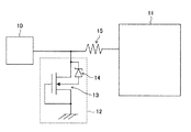
図1は、本実施形態に係る静電放電保護素子を有する回路の回路図である。
例えば、パッド電極10及びそれに接続する内部回路11に対して、静電放電保護素子12が設けられている構成である。静電放電保護素子12は、GG(Grounded Gate)MOSトランジスタ13に対して基板とドレインを接続するツェナーダイオード14が設けられた構成である。
静電放電保護素子12との接続点と内部回路11の間に抵抗素子15が設けられている。
<First Embodiment>
[overall structure]
FIG. 1 is a circuit diagram of a circuit having an electrostatic discharge protection element according to this embodiment.
For example, the electrostatic
A
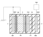
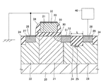
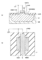
図2は図1に係る静電放電保護回路部分の平面図であり、図3は図2中X−X’における断面図である。
例えば、P型の半導体基板20に、P型ウェルである第1半導体領域21(PW)と、N型ウェルである第2半導体領域22(NW1)及び第3半導体領域23(NW2)が設けられている。
活性領域を除く半導体基板20の表層にSTI(Shallow Trench Isolation)型の素子分離絶縁膜24(I)が形成されている。
ここでは、第1半導体領域21から所定の距離を離間した第3半導体領域23の表層部においても、素子分離絶縁膜24が形成されている。
2 is a plan view of the electrostatic discharge protection circuit portion according to FIG. 1, and FIG. 3 is a cross-sectional view taken along the line XX ′ in FIG.
For example, a P-
An STI (Shallow Trench Isolation) type element isolation insulating film 24 (I) is formed on the surface layer of the
Here, the element
第1半導体領域23の上層にゲート絶縁膜31を介してポリシリコンなどからなるゲート電極32(G)が形成されている。ゲート電極32の上面に高融点金属シリサイド層33が形成されている。
また、ゲート電極32の一方の側面に酸化シリコンなどからなるサイドウォール絶縁膜34(SD)が形成されている。サイドウォール絶縁膜34の側部における第2半導体領域22の表層部に高濃度のN型不純物を含有するソース領域26(NSD1)が形成されている。
ソース領域26の上面に高融点金属シリサイド層27が形成されている。
A gate electrode 32 (G) made of polysilicon or the like is formed on the
Further, a sidewall insulating film 34 (SD) made of silicon oxide or the like is formed on one side surface of the
A refractory
ゲート電極32の他方の側面における半導体基板の表層部において、第1半導体領域21と第3半導体領域23の接合面をまたいで第1半導体領域21と第3半導体領域23にかかるように、N型の第4半導体領域30(POD)が形成されている。
図3に示すように、第4半導体領域30は、ゲート電極32の下部にかかる領域から、第1半導体領域21から所定の距離を離間して形成された素子分離絶縁膜24に至る領域において、形成されている。例えば、ゲート電極32と素子分離絶縁膜24に対して自己整合的に形成されている。
第4半導体領域30の上方及びゲート電極32の他方の側面を被覆するように、窒化シリコンなどからなるシリサイド化防止層35が形成されている。
In the surface layer portion of the semiconductor substrate on the other side surface of the
As shown in FIG. 3, the
A
また、第1半導体領域21から所定の距離を離間して形成された素子分離絶縁膜24を挟んで、第4半導体領域30の反対側における第3半導体領域23の表層部に、高濃度のN型不純物を含有するドレイン領域28(NSD2)が形成されている。
ドレイン領域28の上面に高融点金属シリサイド層29が形成されている。
Further, a high concentration N is formed on the surface layer portion of the
A refractory
また、第1半導体領域21から所定の距離を離間して形成された素子分離絶縁膜24の下部において、高濃度のN型不純物を含有するチャネルストップとなる第5半導体領域25(CS)が形成されている。
In addition, a fifth semiconductor region 25 (CS) serving as a channel stop containing a high-concentration N-type impurity is formed below the element
上記の構成において、ドレイン領域28に接続するように、図1に示す入力パッド40(PAD)及び内部回路などが接続して形成されている。
また、ゲート電極32及びソース領域26が接地されている。
In the above configuration, the input pad 40 (PAD) and the internal circuit shown in FIG. 1 are connected to be connected to the
The
上記の本実施形態の半導体装置の構成において、第4半導体領域30が設けられていることが、図1におけるツェナーダイオードが設けられていることに相当する。
In the configuration of the semiconductor device of the present embodiment, the provision of the
上記の本実施形態の半導体装置においては、入力パッドにサージ電圧が入力された際に、ドレイン領域28と第4半導体領域30との間でツェナー降伏が生じ、第1半導体領域21内にキャリアが注入される。
第1半導体領域21内にキャリアが注入されたことをトリガとして、第1半導体領域21をベース、第2半導体領域22及び第3半導体領域23をそれぞれエミッタ及びコレクタとして構成される横方向の寄生バイポーラトランジスタがオン状態となる。
これによってサージ電圧を放電し、サージ電圧から内部回路を保護することができる。
In the semiconductor device of the present embodiment, a Zener breakdown occurs between the
A lateral parasitic bipolar transistor configured with the
As a result, the surge voltage is discharged, and the internal circuit can be protected from the surge voltage.
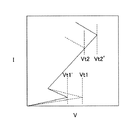
[I−V特性]
図4は印加電圧Vに対するドレイン電流Iを示すI−V特性を示すグラフである。破線は従来例に係り、実線が本実施形態に係る。
上記のように本実施形態においてはツェナー降伏をトリガとして寄生バイポーラトランジスタを動作させることで、図4に示すように、スナップバックが開始電圧Vt1をVt1’へと下げることができる。
これにより、内部回路を確実に保護することができる。
[IV characteristics]
FIG. 4 is a graph showing IV characteristics indicating the drain current I with respect to the applied voltage V. A broken line relates to a conventional example, and a solid line relates to the present embodiment.
As described above, in the present embodiment, by operating the parasitic bipolar transistor using the Zener breakdown as a trigger, the snapback can lower the start voltage Vt1 to Vt1 ′ as shown in FIG.
Thereby, an internal circuit can be protected reliably.
本実施形態においては、第1半導体領域21をベース、第2半導体領域22及び第3半導体領域23をそれぞれエミッタ及びコレクタとして構成される横方向の寄生バイポーラトランジスタの動作でサージ電圧を放電することができる。
例えば、第1半導体領域21、第2半導体領域22及び第3半導体領域23の深さを2μm程度にまで深く形成することで、各PN接合面の大きさを大きくできる。
これにより、接合断面積が大きくかつ接合深さが深いために電流集中が起こりにくく、安定したバイポーラ動作が可能となり、大電流を流すことが可能となる。
In the present embodiment, the surge voltage is discharged by the operation of a lateral parasitic bipolar transistor configured with the
For example, by forming the
As a result, since the junction cross-sectional area is large and the junction depth is deep, current concentration is unlikely to occur, stable bipolar operation becomes possible, and a large current can flow.
例えば、特許文献4、特許文献5などにおいて、急峻なPN接合がシリサイドやコンタクトプラグの近くに存在すると、発生した熱によってそれらの溶融が生じ、保護素子の破壊につながるということが知られている。
本実施形態においては、上記のように、第3半導体領域と、第1半導体領域及び第4半導体領域との接合から、ドレイン領域となる拡散層表面に形成されるシリサイド領域およびコンタクトプラグまでの距離を十分に離すことができる。
これにより、発生した熱によるそれらの溶融の懸念が格段に少なくなる。
図4に示すように、接合部からシリサイドおよびコンタクトプラグまでの距離が十分に離れていることから熱破壊点であるVt2をVt2’に上げることができる。
For example, in Patent Document 4 and Patent Document 5, it is known that when a steep PN junction exists near a silicide or a contact plug, the generated heat causes melting thereof, leading to destruction of the protection element. .
In the present embodiment, as described above, the distance from the junction of the third semiconductor region and the first semiconductor region and the fourth semiconductor region to the silicide region and contact plug formed on the surface of the diffusion layer serving as the drain region. Can be released sufficiently.
As a result, there is much less concern about their melting due to the generated heat.
As shown in FIG. 4, since the distance from the junction to the silicide and the contact plug is sufficiently large, Vt2 which is a thermal breakdown point can be raised to Vt2 ′.
本実施形態の半導体装置においては、例えば、内部回路を構成するMOSトランジスタの通常動作電圧<ドレイン領域と第4半導体領域間の横方向耐圧<寄生バイポーラの耐圧BVceo<内部回路を構成するMOSトランジスタの破壊電圧と設定する。
特に、第4半導体領域とドレイン領域間の横方向耐圧Vthと、寄生バイポーラトランジスタの耐圧BVceoが、Vth<BVceoの関係となっているように設計する。
上記により、通常の電源電圧では寄生バイポーラ動作せず、サージが流入したときのみ内部回路を保護することができる。
In the semiconductor device of the present embodiment, for example, the normal operating voltage of the MOS transistor constituting the internal circuit <the lateral breakdown voltage between the drain region and the fourth semiconductor region <the parasitic bipolar breakdown voltage BVceo <the MOS transistor constituting the internal circuit. Set to breakdown voltage.
In particular, the lateral breakdown voltage Vth between the fourth semiconductor region and the drain region and the breakdown voltage BVceo of the parasitic bipolar transistor are designed to have a relationship of Vth <BVceo.
As described above, the parasitic circuit does not operate at a normal power supply voltage, and the internal circuit can be protected only when a surge flows.
上記各電圧の大小関係により他に制御回路や駆動回路が不要である。
上記の横方向耐圧は、例えばゲート電極から所定の距離を離間して形成された素子分離絶縁膜により隔てられた長さL(図3参照)、素子分離絶縁膜の深さ、あるいはその両方などで制御することができる。
No other control circuit or drive circuit is required due to the magnitude relationship between the voltages.
The lateral withstand voltage is, for example, the length L (see FIG. 3) separated by the element isolation insulating film formed at a predetermined distance from the gate electrode, the depth of the element isolation insulating film, or both Can be controlled.
また、上記のようにチャネルストップとなる第5半導体領域25(CS)を設けることで、これが無い場合と比較して素子分離絶縁膜の幅を狭くでき、デバイスサイズを縮小することができる。 Further, by providing the fifth semiconductor region 25 (CS) serving as a channel stop as described above, the width of the element isolation insulating film can be narrowed and the device size can be reduced as compared with the case where there is no channel stop.
本実施形態において、各半導体領域の導電型を逆にしても、上記と同様に適用可能である。 In this embodiment, even if the conductivity type of each semiconductor region is reversed, the present invention can be applied in the same manner as described above.
本実施形態の半導体装置は、第1半導体領域と前記第3半導体領域にかかるように第4半導体領域が形成されている。
入力パッドにサージ電圧が入力された際にドレイン領域と第4半導体領域との間でツェナー降伏が生じ、第1半導体領域内にキャリアが注入される。これをトリガとして寄生バイポーラトランジスタがオン状態となってサージ電圧を放電することができる。
第4半導体領域は内部回路を構成する領域と同時に形成可能であり、製造効率を向上すると共に、内部回路の保護を的確に行うことが容易に可能である。
In the semiconductor device of this embodiment, the fourth semiconductor region is formed so as to cover the first semiconductor region and the third semiconductor region.
When a surge voltage is input to the input pad, a Zener breakdown occurs between the drain region and the fourth semiconductor region, and carriers are injected into the first semiconductor region. With this as a trigger, the parasitic bipolar transistor is turned on and the surge voltage can be discharged.
The fourth semiconductor region can be formed at the same time as the region constituting the internal circuit, so that the manufacturing efficiency can be improved and the internal circuit can be easily protected accurately.
[製造方法]
本実施形態に係る半導体装置の製造方法について説明する。
例えば、P型の半導体基板20に、活性領域を区分するように、STI(Shallow Trench Isolation)型の素子分離絶縁膜24(I)を形成する。
例えば、深さ400nmの素子分離用溝を形成し、CVD(Chemical Vapor Deposition)法などにより溝を埋め込んで酸化シリコンなどの絶縁膜を堆積し、溝の外部の酸化シリコンを除去することなどで形成できる。
ここでは、図2に示しように、ゲート電極となる領域から所定の距離を離間した位置においても形成する。
[Production method]
A method for manufacturing a semiconductor device according to this embodiment will be described.
For example, an STI (Shallow Trench Isolation) type element isolation insulating film 24 (I) is formed on the P
For example, a trench for element isolation having a depth of 400 nm is formed, the trench is filled by a CVD (Chemical Vapor Deposition) method or the like, an insulating film such as silicon oxide is deposited, and silicon oxide outside the trench is removed. it can.
Here, as shown in FIG. 2, it is also formed at a position spaced a predetermined distance from the region to be the gate electrode.
次に、イオン注入法により、P型ウェルである第1半導体領域21(PW)と、N型ウェルである第2半導体領域22(NW1)及び第3半導体領域23(NW2)を形成する。
イオン注入においては、適宜レジスト膜をパターン形成してマスクとして用いる。
Next, a first semiconductor region 21 (PW) which is a P-type well, a second semiconductor region 22 (NW1) and a third semiconductor region 23 (NW2) which are N-type wells are formed by ion implantation.
In ion implantation, a resist film is appropriately formed and used as a mask.
例えば、下記の条件でそれぞれリンをイオン注入して第2半導体領域22(NW1)及び第3半導体領域23(NW2)を形成する。
(1)2.0MeV、4.0×10¹²/cm2
(2)900keV、6.0×10¹¹/cm2
(3)400keV、7.0×10¹¹/cm2
For example, phosphorus is ion-implanted under the following conditions to form the second semiconductor region 22 (NW1) and the third semiconductor region 23 (NW2).
(1) 2.0 MeV, 4.0 × 10 12 / cm 2
(2) 900 keV, 6.0 × 10 11 / cm 2
(3) 400 keV, 7.0 × 10 11 / cm 2
また、例えば、下記の条件でそれぞれホウ素をイオン注入して第1半導体領域21(PW)を形成する。
(1)1.2MeV、6.0×10¹²/cm2
(2)800keV、3.0×10¹²/cm2
(3)400keV、1.0×10¹²/cm2
(4)150keV、3.0×10¹¹/cm2
上記の第1半導体領域21、第2半導体領域22及び第3半導体領域23は、内部回路を構成する高耐圧MOSトランジスタのウェルを同様にして、同一の工程で形成することができる。
Further, for example, boron is ion-implanted under the following conditions to form the first semiconductor region 21 (PW).
(1) 1.2 MeV, 6.0 × 10 12 / cm 2
(2) 800 keV, 3.0 × 10 12 / cm 2
(3) 400 keV, 1.0 × 10 12 / cm 2
(4) 150 keV, 3.0 × 10 11 / cm 2
The
次に、例えば、素子分離絶縁膜24の下部に、リンを400keV、5.0×10¹²/cm2の条件で注入して第5半導体領域25を形成する。
Next, for example, phosphorus is implanted under the conditions of 400 keV and 5.0 × 10 12 / cm 2 under the element
次に、例えば、熱酸化法などにより第1半導体領域21を含む半導体基板の表面に酸化シリコンを60nmの膜厚で形成し、ゲート絶縁膜31を形成する。
次に、例えばCVD法によりポリシリコンを成膜し、ゲート電極32をパターン形成する。
Next, for example, silicon oxide is formed to a thickness of 60 nm on the surface of the semiconductor substrate including the
Next, for example, a polysilicon film is formed by the CVD method, and the
次に、ゲート電極32と素子分離絶縁膜24の間の領域において、ホウ素をイオン注入して、自己整合的に第4半導体領域30を形成する。この条件は、例えば、40keV、3.5×10¹²/cm2とする。
また、ゲート電極32に対して、リンを20keV、4.0×10¹⁵/cm2の条件で注入する。
Next, boron is ion-implanted in a region between the
Further, phosphorus is implanted into the
次に、例えばCVD法により窒化シリコンを堆積し、第4半導体領域30を被覆する部分を残すようにパターン加工することで、シリサイド化防止層35を形成する。
次に、例えばCVD法により酸化シリコンを堆積し、ゲート電極32の第2半導体領域22側の側面を被覆する部分を残すようにエッチバックすることで、サイドウォール絶縁膜34を形成する。
Next, for example, silicon nitride is deposited by the CVD method, and patterning is performed so as to leave a portion covering the
Next, silicon oxide is deposited by, eg, CVD, and etched back so as to leave a portion covering the side surface of the
次に、サイドウォール絶縁膜34及び素子分離絶縁膜24をマスクとして、リンをイオン注入して、自己整合的にソース領域26及びドレイン領域28を形成する。この条件は、例えば、10keV、4.0×10¹⁵/cm2とする。
次に、例えばスパッタリング法によりタングステンなどの高融点金属を全面に堆積し、シリサイド化のためのアニール処理を行うことで、シリコンまたはポリシリコンが露出していた面上に高融点金属シリサイド層(27,29,33)を形成する。
その後、シリサイド化しなかった未反応の高融点金属を除去する。
Next, phosphorus is ion-implanted using the
Next, a refractory metal such as tungsten is deposited on the entire surface by sputtering, for example, and an annealing process for silicidation is performed, whereby a refractory metal silicide layer (27 , 29, 33).
Thereafter, the unreacted refractory metal that has not been silicided is removed.
次に、中間絶縁膜の形成及びコンタクトホールの開口、プラグ及び上層配線の形成などにより、ドレイン領域28に入力パッド40(PAD)及び内部回路などを接続し、ゲート電極32及びソース領域26を接地する。
Next, the input pad 40 (PAD) and internal circuits are connected to the
上記において、内部回路が内部回路トランジスタを含んでおり、第4半導体領域30を形成するステップを、内部回路トランジスタを構成する不純物半導体領域を形成する工程と同時に行うことが好ましい。
従来例に係る製造方法と比較して、工程の数を増加させないで、本実施形態の半導体装置を製造することができる。
In the above, it is preferable that the internal circuit includes an internal circuit transistor, and the step of forming the
Compared with the manufacturing method according to the conventional example, the semiconductor device of this embodiment can be manufactured without increasing the number of steps.
本実施形態の半導体装置の製造方法は、第1半導体領域と前記第3半導体領域にかかるように形成する第4半導体領域としては、内部回路を構成する領域と同時に形成可能であり、製造効率を向上すると共に、内部回路の保護を的確に行うことが容易に可能である。 In the manufacturing method of the semiconductor device of this embodiment, the fourth semiconductor region formed so as to cover the first semiconductor region and the third semiconductor region can be formed simultaneously with the region constituting the internal circuit, and the manufacturing efficiency is improved. In addition to the improvement, it is easy to accurately protect the internal circuit.
<第1変形例>
図5は第1変形例に係る半導体装置の平面図である。
ソース領域(NSD1)がドレイン領域(NSD2)の外周を囲むようなレイアウトで設けられている。ソース領域(NSD1)とドレイン領域(NSD2)の間に、ゲート電極(G)及び第4半導体領域(POD)などがレイアウトされている。
ここでは、各領域が矩形の形状となっている。
上記のような構成では、矩形の各辺の方向からサージ電圧のチャージを引き抜くことができ、チャージを引き抜く効率を高めることができる。
<First Modification>
FIG. 5 is a plan view of a semiconductor device according to a first modification.
The source region (NSD1) is provided in a layout that surrounds the outer periphery of the drain region (NSD2). A gate electrode (G), a fourth semiconductor region (POD), and the like are laid out between the source region (NSD1) and the drain region (NSD2).
Here, each region has a rectangular shape.
In the configuration as described above, the surge voltage can be extracted from the direction of each side of the rectangle, and the efficiency of extracting the charge can be increased.
<第2変形例>
図6は第2変形例に係る半導体装置の平面図である。
ソース領域(NSD1)がドレイン領域(NSD2)の外周を囲むようなレイアウトで設けられている。ソース領域(NSD1)とドレイン領域(NSD2)の間に、ゲート電極(G)及び第4半導体領域(POD)などがレイアウトされており、特に、ドレイン領域(NSD2)とソース領域(NSD1)がいずれの場所でも等距離を離間した同心円状のレイアウトで設けられている。
上記のような構成では、全ての方向からサージ電圧のチャージを引き抜くことができ、チャージを引き抜く効率を高めることができる。
<Second Modification>
FIG. 6 is a plan view of a semiconductor device according to a second modification.
The source region (NSD1) is provided in a layout that surrounds the outer periphery of the drain region (NSD2). A gate electrode (G), a fourth semiconductor region (POD), and the like are laid out between the source region (NSD1) and the drain region (NSD2), and in particular, the drain region (NSD2) and the source region (NSD1) Are also provided in a concentric layout at equal distances.
In the configuration as described above, the surge voltage can be extracted from all directions, and the efficiency of extracting the charge can be improved.
<第2実施形態>
図7は本実施形態に係る半導体装置の断面図である。
第1実施形態の半導体装置と同様に、ゲート電極32のソース領域26側にサイドウォール絶縁膜34が形成されており、ソース領域26がサイドウォール絶縁膜34に対して自己整合的に形成されている。
本実施形態においては、さらに、ゲート電極32のドレイン領域28側においてもサイドウォール絶縁膜50が形成されている。
また、サイドウォール絶縁膜50に対して自己整合的に、P型の導電性不純物を第4半導体領域30より高濃度に含有する第6半導体領域51が、第4半導体領域30に接続して形成されている。
第6半導体領域51の表面に高融点金属シリサイド層52が形成されている。
ここで、第6半導体領域51が形成されていることにより、第4半導体領域30は実質的にゲート電極32の下部にのみ残された状態となっている。
Second Embodiment
FIG. 7 is a cross-sectional view of the semiconductor device according to the present embodiment.
Similar to the semiconductor device of the first embodiment, a
In the present embodiment, a
In addition, a
A refractory
Here, since the
上記の本実施形態に係る半導体装置は、第1実施形態の半導体装置と同様に形成できる。
即ち、サイドウォール絶縁膜34と同時にサイドウォール絶縁膜50を形成し、サイドウォール絶縁膜50に対して自己整合的に、P型の導電性不純物を第4半導体領域30より高濃度にイオン注入して、第6半導体領域51を形成する。
上記を除いて、第1実施形態の半導体装置と同様に形成できる。
The semiconductor device according to this embodiment can be formed in the same manner as the semiconductor device of the first embodiment.
That is, a
Except for the above, it can be formed similarly to the semiconductor device of the first embodiment.
上記の第1半導体領域21、第2半導体領域22及び第3半導体領域23は、第1実施形態と同様に、内部回路を構成する高耐圧MOSトランジスタのウェルを同様にして、同一の工程で形成することができる。
あるいは、本実施形態においては、内部回路を構成する低耐圧の通常のMOSトランジスタのウェルを同様にして、同一の工程で形成することもできる。
The
Alternatively, in this embodiment, the well of a low-breakdown voltage normal MOS transistor that constitutes an internal circuit can be formed in the same process in the same manner.
本実施形態の半導体装置は、第1半導体領域と第3半導体領域にかかるように第4半導体領域が形成されている。
入力パッドにサージ電圧が入力された際にドレイン領域と第4半導体領域との間でツェナー降伏が生じ、第1半導体領域内にキャリアが注入される。
これをトリガとして寄生バイポーラトランジスタがオン状態となってサージ電圧を放電することができる。
第4半導体領域は内部回路を構成する領域と同時に形成可能であり、製造効率を向上すると共に、内部回路の保護を的確に行うことが容易に可能である。
In the semiconductor device of this embodiment, the fourth semiconductor region is formed so as to cover the first semiconductor region and the third semiconductor region.
When a surge voltage is input to the input pad, a Zener breakdown occurs between the drain region and the fourth semiconductor region, and carriers are injected into the first semiconductor region.
With this as a trigger, the parasitic bipolar transistor is turned on and the surge voltage can be discharged.
The fourth semiconductor region can be formed at the same time as the region constituting the internal circuit, so that the manufacturing efficiency can be improved and the internal circuit can be easily protected accurately.
本実施形態の半導体装置の製造方法は、第1半導体領域と第3半導体領域にかかるように形成する第4半導体領域としては、内部回路を構成するトランジスタのP型領域と同時に形成可能である。製造効率を向上すると共に、内部回路の保護を的確に行うことが容易に可能である。 In the manufacturing method of the semiconductor device of this embodiment, the fourth semiconductor region formed so as to cover the first semiconductor region and the third semiconductor region can be formed simultaneously with the P-type region of the transistor constituting the internal circuit. It is easy to improve the manufacturing efficiency and protect the internal circuit accurately.
<第3変形例>
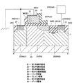
図8は第3変形例に係る半導体装置の断面図である。
ゲート電極32のソース領域26側の側面における半導体基板の表層部において、第1半導体領域21と第2半導体領域22の接合面をまたいで第1半導体領域21と第2半導体領域22にかかるように、N型の第7半導体領域60(NOD)が形成されている。
これを除いて、第1実施形態の半導体装置と同様である。
また、第7半導体領域60の上方及びゲート電極32のソース領域26側の側面を被覆するように、窒化シリコンなどからなるシリサイド化防止層61が形成されている。
N型の第7半導体領域60(NOD)は、P型の第4半導体領域30(POD)と同様にして反対の導電型の不純物をイオン注入して形成することができる。
シリサイド化防止層61は、シリサイド化防止層35と同じ工程で形成することができる。
本変形例の半導体装置は、第1半導体領域と、第2半導体領域及び第7半導体領域との接合から、ソース領域となる拡散層表面に形成されるシリサイド領域およびコンタクトプラグまでの距離を十分に離すことができる。
これにより、発生した熱によるそれらの溶融の懸念が格段に少なくなる。
<Third Modification>
FIG. 8 is a cross-sectional view of a semiconductor device according to a third modification.
In the surface layer portion of the semiconductor substrate on the side surface of the
Except this, it is the same as the semiconductor device of the first embodiment.
A
The N-type seventh semiconductor region 60 (NOD) can be formed by ion implantation of impurities of the opposite conductivity type in the same manner as the P-type fourth semiconductor region 30 (POD).
The
The semiconductor device of this modification has a sufficient distance from the junction of the first semiconductor region, the second semiconductor region, and the seventh semiconductor region to the silicide region and contact plug formed on the surface of the diffusion layer serving as the source region. Can be released.
As a result, there is much less concern about their melting due to the generated heat.
<第4変形例>
図9は第4変形例に係る半導体装置の断面図である。
第3変形例の半導体装置と同様であるが、第2半導体領域22及び第3半導体領域23の下部に、N型の第8半導体領域70及び第9半導体領域71がそれぞれ設けられていることが異なる。
上記のほか、第3変形例と同様に、N型の第7半導体領域60(NOD)とシリサイド化防止層61が形成されている。
第8半導体領域70及び第9半導体領域71は、N型不純物の実効的濃度が第2半導体領域22及び第3半導体領域23より高い。
また、第8半導体領域70及び第9半導体領域71の間隔は、第2半導体領域22及び第3半導体領域23の間隔、即ち、第1半導体領域21の幅より狭く設けられている。
これによって、より詳細に寄生トランジスタの動作電圧などを制御することができる。
<Fourth Modification>
FIG. 9 is a sectional view of a semiconductor device according to a fourth modification.
Although it is the same as that of the semiconductor device of the third modification, an N-type
In addition to the above, an N-type seventh semiconductor region 60 (NOD) and a
The
Further, the interval between the
As a result, the operating voltage of the parasitic transistor can be controlled in more detail.
本発明は上記の説明に限定されない。
例えば、MOS型のESD保護素子を有する半導体装置を想定しているが、それ以外の半導体装置に適用することも可能である。
また、本発明は、静電放電保護素子のみとしても適用可能である。
その他、本発明の要旨を逸脱しない範囲で、種々の変更が可能である。
The present invention is not limited to the above description.
For example, although a semiconductor device having a MOS type ESD protection element is assumed, the present invention can also be applied to other semiconductor devices.
Further, the present invention can be applied only as an electrostatic discharge protection element.
In addition, various modifications can be made without departing from the scope of the present invention.
10…パッド電極、11…内部回路、12…静電放電保護素子、13…GGMOSトランジスタ、14…ツェナーダイオード、15…抵抗素子、20…半導体基板、21…半導体領域、22…第2半導体領域、23…第3半導体領域、24…素子分離絶縁膜、25…第5半導体領域、26…ソース領域、27…高融点金属シリサイド層、28…ドレイン領域、29…高融点金属シリサイド層、30…第4半導体領域、31…ゲート絶縁膜、32…ゲート電極、33…高融点金属シリサイド層、34…サイドウォール絶縁膜、35…シリサイド化防止層、40…パッド電極、50…サイドウォール絶縁膜、51…第6半導体領域、52…高融点金属シリサイド層、60…第7半導体領域、61…シリサイド化防止層、70…第8半導体領域、71…第9半導体領域
DESCRIPTION OF
Claims (14)
を有しており、
前記静電放電保護素子は、
半導体基板に形成された第1導電型の第1半導体領域と、
前記第1半導体領域と接合するように前記第1半導体領域の両側に形成された第2導電型の第2半導体領域及び第3半導体領域と、
前記第1半導体領域の上方に絶縁膜を介して形成されたゲート電極と、
前記半導体基板の表層部において前記第1半導体領域と前記第3半導体領域の接合面をまたいで前記第1半導体領域と前記第3半導体領域にかかるように形成された第1導電型の第4半導体領域と、
前記第2半導体領域の表層部に形成された第2導電型のソース領域と、
前記第4半導体領域から所定の距離を離間して前記第3半導体領域の表層部に形成された第2導電型のドレイン領域と、
前記第4半導体領域と前記ドレイン領域の間の領域において前記半導体基板の表層部に形成された素子分離絶縁膜と
を有し、
前記ゲート電極及び前記ソース領域が接地されており、
前記内部回路に接続された入力パッドが前記ドレイン領域に接続して形成されており、
前記入力パッドにサージ電圧が入力された際に、前記ドレイン領域と前記第4半導体領域との間でツェナー降伏が生じ、前記第1半導体領域内にキャリアが注入され、当該第1半導体領域内に前記キャリアが注入されたことをトリガとして前記第1半導体領域、前記第2半導体領域及び前記第3半導体領域で構成される寄生バイポーラトランジスタがオン状態となって前記サージ電圧を放電し、前記サージ電圧から前記内部回路を保護する
半導体装置。 It has an electrostatic discharge protection element that protects the internal circuit.
The electrostatic discharge protection element is:
A first semiconductor region of a first conductivity type formed on a semiconductor substrate;
A second conductivity type second semiconductor region and a third semiconductor region formed on both sides of the first semiconductor region so as to be joined to the first semiconductor region;
A gate electrode formed above the first semiconductor region via an insulating film;
A first conductivity type fourth semiconductor formed over the first semiconductor region and the third semiconductor region across the junction surface of the first semiconductor region and the third semiconductor region in the surface layer portion of the semiconductor substrate. Area,
A source region of a second conductivity type formed in a surface layer portion of the second semiconductor region;
A drain region of a second conductivity type formed in a surface layer portion of the third semiconductor region at a predetermined distance from the fourth semiconductor region;
An element isolation insulating film formed in a surface layer portion of the semiconductor substrate in a region between the fourth semiconductor region and the drain region;
The gate electrode and the source region are grounded;
An input pad connected to the internal circuit is formed connected to the drain region,
When a surge voltage is input to the input pad, a Zener breakdown occurs between the drain region and the fourth semiconductor region, carriers are injected into the first semiconductor region, and the first semiconductor region is injected into the first semiconductor region. A parasitic bipolar transistor composed of the first semiconductor region, the second semiconductor region, and the third semiconductor region is turned on when the carrier is injected to discharge the surge voltage, and the surge voltage A semiconductor device for protecting the internal circuit from the semiconductor device.
請求項1に記載の半導体装置。 The semiconductor device according to claim 1, wherein the fourth semiconductor region is formed in a self-aligned manner with respect to the gate electrode and the element isolation insulating film.
請求項1に記載の半導体装置。 The semiconductor device according to claim 1, wherein a fifth semiconductor region of a second conductivity type is formed in the semiconductor substrate below the element isolation insulating film.
Vth<BVceo
の関係となっている
請求項1記載の半導体装置。 The lateral withstand voltage Vth between the fourth semiconductor region and the drain region and the withstand voltage BVceo of the parasitic bipolar transistor are Vth <BVceo.
The semiconductor device according to claim 1, wherein:
Vth<BVceo
の関係となるように、前記素子分離絶縁膜の距離、深さ、あるいはその両方が規定されている
請求項1記載の半導体装置。 The lateral withstand voltage Vth between the fourth semiconductor region and the drain region and the withstand voltage BVceo of the parasitic bipolar transistor are Vth <BVceo.
The semiconductor device according to claim 1, wherein a distance, a depth, or both of the element isolation insulating film are defined so as to satisfy the following relationship.
前記ソース領域が前記サイドウォール絶縁膜に対して自己整合的に形成されている
請求項1記載の半導体装置。 A sidewall insulating film is formed on the source region side of the gate electrode,
The semiconductor device according to claim 1, wherein the source region is formed in a self-aligned manner with respect to the sidewall insulating film.
前記サイドウォール絶縁膜に対して自己整合的に、第1導電型の導電性不純物を前記第4半導体領域より高濃度に含有する第6半導体領域が前記第4半導体領域に接続して形成されている
請求項1記載の半導体装置。 A sidewall insulating film is formed on the drain region side of the gate electrode,
A sixth semiconductor region containing conductive impurities of the first conductivity type in a higher concentration than the fourth semiconductor region is connected to the fourth semiconductor region in a self-aligned manner with respect to the sidewall insulating film. The semiconductor device according to claim 1.
請求項1記載の半導体装置。 The semiconductor device according to claim 1, wherein the source region is provided in a layout surrounding an outer periphery of the drain region.
請求項1記載の半導体装置。 2. The semiconductor device according to claim 1, wherein the source region is provided so as to surround an outer periphery of the drain region, and the drain region and the source region are provided in a concentric layout separated at equal distances at any location.
を有しており、
半導体基板に、第1導電型の第1半導体領域を形成し、前記第1半導体領域と接合するように前記第1半導体領域の両側に第2導電型の第2半導体領域及び第3半導体領域を形成するステップと、
前記第3半導体領域において前記第1半導体領域と前記第3半導体領域の接合面から所定の距離を離間するように前記半導体基板の表層部に素子分離絶縁膜を形成するステップと、
前記第1半導体領域の上方に絶縁膜を介してゲート電極を形成するステップと、
前記ゲート電極と前記素子分離絶縁膜の間の領域における前記半導体基板の表層部において前記第1半導体領域と前記第3半導体領域の接合面をまたいで前記第1半導体領域と前記第3半導体領域にかかるように第1導電型の第4半導体領域を形成するステップと、
前記第2半導体領域の表層部に第2導電型のソース領域を形成するステップと、
前記第4半導体領域が設けられた側と反対側における前記第3半導体領域の表層部に第2導電型のドレイン領域を形成するステップと、
前記ゲート電極及び前記ソース領域を接地するように接続し、前記内部回路に接続された入力パッドが前記ドレイン領域に接続するステップと
を有する
半導体装置の製造方法。 An electrostatic discharge protection element forming step for forming an electrostatic discharge protection element for protecting an internal circuit,
A first conductive type first semiconductor region is formed on a semiconductor substrate, and a second conductive type second semiconductor region and a third semiconductor region are formed on both sides of the first semiconductor region so as to be joined to the first semiconductor region. Forming step;
Forming an element isolation insulating film on a surface layer portion of the semiconductor substrate so as to be separated from a bonding surface between the first semiconductor region and the third semiconductor region in the third semiconductor region;
Forming a gate electrode above the first semiconductor region through an insulating film;
In the surface layer portion of the semiconductor substrate in the region between the gate electrode and the element isolation insulating film, the first semiconductor region and the third semiconductor region are crossed over the junction surface of the first semiconductor region and the third semiconductor region. Forming a first conductivity type fourth semiconductor region in such a manner;
Forming a second conductivity type source region in a surface layer portion of the second semiconductor region;
Forming a drain region of the second conductivity type in a surface layer portion of the third semiconductor region on the side opposite to the side where the fourth semiconductor region is provided;
Connecting the gate electrode and the source region to be grounded, and connecting an input pad connected to the internal circuit to the drain region.
前記第4半導体領域を形成するステップを、前記内部回路トランジスタを構成する不純物半導体領域を形成する工程と同時に行う
請求項10記載の半導体装置の製造方法。 The internal circuit includes an internal circuit transistor;
The method of manufacturing a semiconductor device according to claim 10, wherein the step of forming the fourth semiconductor region is performed simultaneously with the step of forming an impurity semiconductor region constituting the internal circuit transistor.
請求項10に記載の半導体装置の製造方法。 The method of manufacturing a semiconductor device according to claim 10, wherein in the step of forming the fourth semiconductor region, the fourth semiconductor region is formed in a self-aligned manner with respect to the gate electrode and the element isolation insulating film.
請求項10に記載の半導体装置の製造方法。 The method of manufacturing a semiconductor device according to claim 10, further comprising forming a fifth semiconductor region of a second conductivity type in the semiconductor substrate below the element isolation insulating film.
前記第1半導体領域と接合するように前記第1半導体領域の両側に形成された第2導電型の第2半導体領域及び第3半導体領域と、
前記第1半導体領域の上方に絶縁膜を介して形成されたゲート電極と、
前記半導体基板の表層部において前記第1半導体領域と前記第3半導体領域の接合面をまたいで前記第1半導体領域と前記第3半導体領域にかかるように形成された第1導電型の第4半導体領域と、
前記第2半導体領域の表層部に形成された第2導電型のソース領域と、
前記第4半導体領域から所定の距離を離間して前記第3半導体領域の表層部に形成された第2導電型のドレイン領域と、
前記第4半導体領域と前記ドレイン領域の間の領域において前記半導体基板の表層部に形成された素子分離絶縁膜と
を有し、
前記ゲート電極及び前記ソース領域が接地されており、
入力パッドが前記ドレイン領域に接続して形成されており、
前記入力パッドにサージ電圧が入力された際に、前記ドレイン領域と前記第4半導体領域との間でツェナー降伏が生じ、前記第1半導体領域内にキャリアが注入され、当該第1半導体領域内に前記キャリアが注入されたことをトリガとして前記第1半導体領域、前記第2半導体領域及び前記第3半導体領域で構成される寄生バイポーラトランジスタがオン状態となって前記サージ電圧を放電する
静電放電保護素子。 A first semiconductor region of a first conductivity type formed on a semiconductor substrate;
A second conductivity type second semiconductor region and a third semiconductor region formed on both sides of the first semiconductor region so as to be joined to the first semiconductor region;
A gate electrode formed above the first semiconductor region via an insulating film;
A first conductivity type fourth semiconductor formed over the first semiconductor region and the third semiconductor region across the junction surface of the first semiconductor region and the third semiconductor region in the surface layer portion of the semiconductor substrate. Area,
A source region of a second conductivity type formed in a surface layer portion of the second semiconductor region;
A drain region of a second conductivity type formed in a surface layer portion of the third semiconductor region at a predetermined distance from the fourth semiconductor region;
An element isolation insulating film formed in a surface layer portion of the semiconductor substrate in a region between the fourth semiconductor region and the drain region;
The gate electrode and the source region are grounded;
An input pad is formed connected to the drain region,
When a surge voltage is input to the input pad, a Zener breakdown occurs between the drain region and the fourth semiconductor region, carriers are injected into the first semiconductor region, and the first semiconductor region is injected into the first semiconductor region. An electrostatic discharge protection in which a parasitic bipolar transistor composed of the first semiconductor region, the second semiconductor region, and the third semiconductor region is turned on to discharge the surge voltage triggered by the injection of the carrier element.
Priority Applications (1)
| Application Number | Priority Date | Filing Date | Title |
|---|---|---|---|
| JP2008314307A JP2010141007A (en) | 2008-12-10 | 2008-12-10 | Semiconductor device, method of manufacturing the same, and electrostatic discharge protective element |
Applications Claiming Priority (1)
| Application Number | Priority Date | Filing Date | Title |
|---|---|---|---|
| JP2008314307A JP2010141007A (en) | 2008-12-10 | 2008-12-10 | Semiconductor device, method of manufacturing the same, and electrostatic discharge protective element |
Publications (1)
| Publication Number | Publication Date |
|---|---|
| JP2010141007A true JP2010141007A (en) | 2010-06-24 |
Family
ID=42350904
Family Applications (1)
| Application Number | Title | Priority Date | Filing Date |
|---|---|---|---|
| JP2008314307A Pending JP2010141007A (en) | 2008-12-10 | 2008-12-10 | Semiconductor device, method of manufacturing the same, and electrostatic discharge protective element |
Country Status (1)
| Country | Link |
|---|---|
| JP (1) | JP2010141007A (en) |
Cited By (1)
| Publication number | Priority date | Publication date | Assignee | Title |
|---|---|---|---|---|
| WO2012120802A1 (en) * | 2011-03-09 | 2012-09-13 | ルネサスエレクトロニクス株式会社 | Semiconductor device |
-
2008
- 2008-12-10 JP JP2008314307A patent/JP2010141007A/en active Pending
Cited By (1)
| Publication number | Priority date | Publication date | Assignee | Title |
|---|---|---|---|---|
| WO2012120802A1 (en) * | 2011-03-09 | 2012-09-13 | ルネサスエレクトロニクス株式会社 | Semiconductor device |
Similar Documents
| Publication | Publication Date | Title |
|---|---|---|
| US9401352B2 (en) | Field-effect device and manufacturing method thereof | |
| US6639284B1 (en) | Compensated-well electrostatic discharge protection structure | |
| JP3675303B2 (en) | Semiconductor device with built-in electrostatic protection circuit and manufacturing method thereof | |
| TWI259573B (en) | High efficiency substrate-triggered ESD protection component | |
| TWI415223B (en) | Semiconductor device and manufacturing method thereof | |
| US6987303B2 (en) | Silicon-controlled rectifier structures on silicon-on insulator with shallow trench isolation | |
| US8107203B2 (en) | Electrostatic discharge protection device | |
| US6576959B2 (en) | Device and method of low voltage SCR protection for high voltage failsafe ESD applications | |
| US8471333B2 (en) | Semiconductor device and manufacturing method of the same | |
| JP2006523965A (en) | Low voltage silicon controlled rectifier (SCR) for electrostatic discharge (ESD) protection targeted at silicon on insulator technology | |
| JP4844621B2 (en) | Transistor-type protection device and semiconductor integrated circuit | |
| US6764892B2 (en) | Device and method of low voltage SCR protection for high voltage failsafe ESD applications | |
| JP5525736B2 (en) | Semiconductor device and manufacturing method thereof | |
| US6835985B2 (en) | ESD protection structure | |
| JP6972691B2 (en) | Semiconductor devices and methods for manufacturing semiconductor devices | |
| JP4479041B2 (en) | Semiconductor device and manufacturing method thereof | |
| JP2010141007A (en) | Semiconductor device, method of manufacturing the same, and electrostatic discharge protective element | |
| JP5925419B2 (en) | Offtra ESD protection device and method for manufacturing the same | |
| JP3402244B2 (en) | Semiconductor device including lateral MOS element | |
| JP2017092297A (en) | Field-effect transistor, and semiconductor device | |
| JP5494519B2 (en) | Transistor-type protection device and semiconductor integrated circuit | |
| US20250072018A1 (en) | Semiconductor device and method of manufacturing the same | |
| JP2011171662A (en) | Protective transistor, and semiconductor integrated circuit | |
| JP5416478B2 (en) | Semiconductor device | |
| JP2008098276A (en) | Semiconductor device and manufacturing method thereof |