JP2010123720A - Solar cell backside sheet and solar cell module - Google Patents
Solar cell backside sheet and solar cell module Download PDFInfo
- Publication number
- JP2010123720A JP2010123720A JP2008295373A JP2008295373A JP2010123720A JP 2010123720 A JP2010123720 A JP 2010123720A JP 2008295373 A JP2008295373 A JP 2008295373A JP 2008295373 A JP2008295373 A JP 2008295373A JP 2010123720 A JP2010123720 A JP 2010123720A
- Authority
- JP
- Japan
- Prior art keywords
- solar cell
- concavo
- light
- resin
- layer
- Prior art date
- Legal status (The legal status is an assumption and is not a legal conclusion. Google has not performed a legal analysis and makes no representation as to the accuracy of the status listed.)
- Withdrawn
Links
Images


Classifications
-
- Y—GENERAL TAGGING OF NEW TECHNOLOGICAL DEVELOPMENTS; GENERAL TAGGING OF CROSS-SECTIONAL TECHNOLOGIES SPANNING OVER SEVERAL SECTIONS OF THE IPC; TECHNICAL SUBJECTS COVERED BY FORMER USPC CROSS-REFERENCE ART COLLECTIONS [XRACs] AND DIGESTS
- Y02—TECHNOLOGIES OR APPLICATIONS FOR MITIGATION OR ADAPTATION AGAINST CLIMATE CHANGE
- Y02E—REDUCTION OF GREENHOUSE GAS [GHG] EMISSIONS, RELATED TO ENERGY GENERATION, TRANSMISSION OR DISTRIBUTION
- Y02E10/00—Energy generation through renewable energy sources
- Y02E10/50—Photovoltaic [PV] energy
- Y02E10/52—PV systems with concentrators
Abstract
Description
本発明は、反射面を有する凹凸構造が形成され、前記構造によって光を反射し、本来は損失となる光を有効に活用できる裏面シート及びそれを用いた太陽電池モジュールに関する。 The present invention relates to a back sheet that has a concavo-convex structure having a reflecting surface, reflects light by the structure, and can effectively use light that is originally lost, and a solar cell module using the back sheet.
近年、太陽電池モジュールの普及は大きな広がりを見せ、電卓等の小型電子機器に搭載される比較的小さなものから、家庭用として住宅に取り付けられる太陽電池モジュールや大規模な発電施設に用いられる大面積の太陽電池発電システム、さらには人工衛星の電源まで、様々な分野で利用が促進されている(例えば、特許文献1参照)。 In recent years, the widespread use of solar cell modules has expanded greatly, from relatively small ones mounted on small electronic devices such as calculators to large areas used for solar cell modules installed in homes and large-scale power generation facilities The use of solar cell power generation systems and power supplies for artificial satellites has been promoted in various fields (see, for example, Patent Document 1).
太陽電池は、主に光が照射される面積に比例して発電量が増加する。したがって、発電効率を向上させるには封止技術、製膜技術等の製造技術を改善することに加え、いかにして太陽電池モジュールの開口率、すなわち全面積に対する発電可能な面積の割合を大きくするかが重要な課題となっている。 In the solar cell, the amount of power generation increases mainly in proportion to the area irradiated with light. Therefore, in order to improve the power generation efficiency, in addition to improving the manufacturing technology such as the sealing technology and the film forming technology, how to increase the aperture ratio of the solar cell module, that is, the ratio of the power generating area to the total area Is an important issue.
また、特に単結晶シリコンや多結晶のシリコンのでは、そのシリコンのコストが高いという問題がある。また、それを貼り付けるためのコストも加算されてくる。
そこで、太陽電池セルの構成部材であるシリコンの量が少なく、CVD等の技術により、成膜することができるような薄膜シリコンの太陽電池セルが用いられるようになってきている。
In particular, single crystal silicon or polycrystalline silicon has a problem that the cost of the silicon is high. Also, the cost for pasting it is added.
In view of this, the amount of silicon that is a constituent member of a solar cell is small, and a thin-film silicon solar cell that can be formed by a technique such as CVD has been used.
しかし、上述のものは特に赤外の光が薄膜シリコンの太陽電池セルを透過しやすいため光の吸収率が低い。そこで光の利用効率を上げるために、あえて入射光を散乱させて、薄膜シリコンの太陽電池セルを透過する距離を稼ぐことで光の利用効率を向上させる。 However, the light absorption rate of the above-mentioned is particularly low because infrared light is likely to pass through thin-film silicon solar cells. Therefore, in order to increase the light utilization efficiency, the incident light is intentionally scattered to increase the light transmission efficiency by increasing the distance through which the thin-film silicon solar cells are transmitted.
一般に、非晶質シリコン太陽電池には、2種類の構造のものがある。一つは、ガラス等の透光性基板上に、SnO2やITO等の透明電導膜が形成され、その上に非晶質半導体(Si)のp層、i層、n層がこの順に積層されて成る構造のものである。もう一つは、金属基板電極の上に、非晶質半導体(Si)のn層,i層,p層がこの順に積層されて光電変換活性層が形成され、更にその上に透明電導膜が積層され成る構造のものである。 In general, there are two types of amorphous silicon solar cells. First, a transparent conductive film such as SnO2 or ITO is formed on a light-transmitting substrate such as glass, and an amorphous semiconductor (Si) p-layer, i-layer, and n-layer are stacked in this order. It is of the structure which consists of. The other is an amorphous semiconductor (Si) n-layer, i-layer, and p-layer stacked in this order on a metal substrate electrode to form a photoelectric conversion active layer, and a transparent conductive film is further formed thereon. It has a laminated structure.
特に、前者の構造のものでは、非晶質半導体をp−i−n層の順に形成するのに、透光性絶縁基板が太陽電池表面カバーガラスを兼ねることができること、また、SnO2等の耐プラズマ性透明電導膜が開発されて、この上に非晶質半導体光電変換活性層をプラズマCVD法で形成することが可能になったことなどから、現在多く用いられている。
In particular, in the former structure, in order to form amorphous semiconductors in the order of pin layers, the translucent insulating substrate can also serve as a solar cell surface cover glass, and resistance to
なお、非晶質半導光電変換活性層の形成に、原料ガスのグロー放電分解によるプラズマCVD法や、光CVD法による気相成長法を用いることができ、これらの方法によれば大面積の薄膜形成が可能であるという利点もある。 The amorphous semi-light-guided conversion active layer can be formed by using a plasma CVD method by glow discharge decomposition of a source gas or a vapor phase growth method by a photo-CVD method. There is also an advantage that a thin film can be formed.
非晶質Si太陽電池は、100℃〜200℃程度の比較的低温で形成できるので、その非晶質Si太陽電池を形成するための基板として、様々な材質の基板を用いることが可能であるが、通常よく用いられるものはガラス基板やステンレス基板である。 Since an amorphous Si solar cell can be formed at a relatively low temperature of about 100 ° C. to 200 ° C., it is possible to use substrates of various materials as a substrate for forming the amorphous Si solar cell. However, glass substrates and stainless steel substrates are commonly used.
また、非晶質Si太陽電池は、光を電機に代える変換効率が最大となるときのシリコンの光吸収層の膜厚が500nm程度であるため、その変換効率を向上させるには光吸収層の膜厚内で光の吸収量を増大させることが重要なポイントとなる。そのため、ガラス基板上の表面に凹凸のある透明導電膜を形成したり、ステンレス基板上の表面に凹凸のある金属膜を形成したりすることにより、光吸収層中での光の光路長を増加させることが従来より行われてきた。 In addition, the amorphous Si solar cell has a silicon light absorption layer thickness of about 500 nm when the conversion efficiency for replacing light with an electric machine is maximized. Therefore, in order to improve the conversion efficiency of the light absorption layer, Increasing the amount of light absorption within the film thickness is an important point. Therefore, the optical path length of light in the light absorption layer is increased by forming a transparent conductive film with unevenness on the surface of the glass substrate or forming a metal film with unevenness on the surface of the stainless steel substrate. It has been performed conventionally.
このような方法で、光吸収層中での光路長を増加させた太陽電池の場合、その表面に凹凸がない平坦な基板上に非晶質Si太陽電池を形成した場合と比較して、光の利用効率が顕著に向上する。 In the case of the solar cell in which the optical path length in the light absorption layer is increased by such a method, the light is compared with the case where the amorphous Si solar cell is formed on a flat substrate having no irregularities on the surface. The utilization efficiency of is significantly improved.
ところで、ガラス基板の表面上に凹凸を形成する一般的な方法としては、常圧CVD法により透明電極であるSnO2膜を形成する方法があげられる。また、ステンレス等の金属基板上に凹凸を形成する方法としては、Agを蒸着法やスパッタリング法により形成する際に、その形成条件を調整したり、Agの形成後に熱処理を行ったりする方法が用いられていた。
By the way, as a general method for forming irregularities on the surface of a glass substrate, there is a method of forming a
この薄膜太陽電池は、透光性絶縁基板の上に、透明導電膜、水素化アモルファスシリコンカーバイド(a―SiCH)p層、水素化アモルファスシリコン(a―SiH)i層、水素化アモルファスシリコン(a―SiH)n層、透明導電膜、及び裏面電極が順次形成されて構成されるものである。そして、前述のようにして、透明導電膜の表面に凹凸形状が形成され、これによりその上部に形成された各層が凹凸構造を有するというものである。 This thin film solar cell has a transparent conductive film, a hydrogenated amorphous silicon carbide (a-SiCH) p layer, a hydrogenated amorphous silicon (a-SiH) i layer, a hydrogenated amorphous silicon (a —SiH) n layer, transparent conductive film, and back electrode are sequentially formed. Then, as described above, a concavo-convex shape is formed on the surface of the transparent conductive film, whereby each layer formed on the top has a concavo-convex structure.
また、薄膜太陽電池等の半導体素子を可撓性基板あるいは軽量基板上に形成する場合、耐熱性の高いポリイミド樹脂が用いられてきた。このような樹脂に凹凸を形成する方法は、特許文献2等に開示されている。
Moreover, when forming semiconductor elements, such as a thin film solar cell, on a flexible substrate or a lightweight substrate, the polyimide resin with high heat resistance has been used. A method for forming irregularities in such a resin is disclosed in
また、特許文献3には、V溝の周期構造により、光を再帰反射し、光の利用効率を上げるような特許が公開されており、V溝頂角は、50度から90度が望ましいとの記述がある。また、V溝の周期のピッチとしては、10μmから20μmが望ましいとの記述がある。 Further, Patent Document 3 discloses a patent that retroreflects light by the periodic structure of the V-groove to increase the light utilization efficiency, and that the V-groove apex angle is desirably 50 to 90 degrees. There is a description. Further, there is a description that the pitch of the period of the V groove is preferably 10 μm to 20 μm.
また、太陽電池セル30の配置間隔を狭くするとリーク電流が生じてしまうため、隣り合う太陽電池セル30の間の領域が必要となる。図17に示すように、太陽電池モジュール200に入射する光H0のうち、この領域に入射する光H1を、裏面材300を太陽電池モジュール200の背面に配置することにより裏面材300反射し、光H2として再利用するもの(特許文献4)が知られている。しかし、まだ十分な発電効率は得られていない。
上述のように、従来の太陽電池モジュールは、単位面積当たりの発電効率を上げようという要望は多いが、損失となってしまう光があるため、まだ十分とはいえない。 As described above, the conventional solar cell module has many requests to increase the power generation efficiency per unit area, but it is not yet sufficient because there is light that causes loss.
本発明はこのような課題に鑑みてなされたものであって、本来は損失となってしまう光を再利用することによって、光の利用効率を向上させることができる裏面シート及びそれを用いた太陽電池モジュール用を提供することを目的とする。 The present invention has been made in view of such problems, and a back sheet that can improve light use efficiency by reusing light that would otherwise be lost, and a sun using the back sheet An object is to provide a battery module.
上述の目的を達成するために、本発明では、以下のような手段を講じる。 In order to achieve the above object, the present invention takes the following measures.
請求項1の発明は、
少なくとも透光性前面板と太陽電池セルと封止材と裏面シートとを有する太陽電池モジュールにおいて、
前記裏面シートの前面側に光散乱反射機能を有する凹凸構造が形成されていることを特徴とする太陽電池裏面シートである。
請求項2の発明は、
前記凹凸構造の表面にのみ、散乱要素を含む樹脂層が形成されていることを特徴とする請求項1に記載の太陽電池裏面シートである。
請求項3の発明は、
前記凹凸構造が、散乱要素を含む樹脂層から構成されることを特徴とする請求項1記載の太陽電池裏面シートである。
請求項4の発明は、
前記散乱要素が、白色顔料、金属粒子、高屈折率粒子、中空粒子、のいずれかからなることを特徴とする請求項1乃至3の何れか1項に記載の太陽電池裏面シートである。
請求項5の発明は、
前記裏面シートが、前記凹凸構造の前面側に前記凹凸構造を保護するトップコート層を有することを特徴とする請求項1乃至4の何れか1項に記載の太陽電池裏面シートである。
請求項6の発明は、
前記トップコート層が、電気絶縁性を有し、絶縁破壊電圧が3KV以上であることを特徴とする請求項1乃至5の何れか1項に記載の太陽電池裏面シートである。
請求項7の発明は、
繰り返しからなる周期構造を有する前記凹凸構造が、プリズム、多角錐形状、シリンドリカルレンズ、マイクロレンズ、あるいはこれらの逆型のいずれかであることを特徴とする請求項1乃至6の何れか1項に記載の太陽電池裏面シートである。
請求項8の発明は、
繰り返しからなる周期構造を有する前記凹凸構造の単位構造の底辺と高さのアスペクト比が、0.15以上0.4以下であることを特徴とする請求項1乃至7の何れか1項に記載の太陽電池裏面シートである。
請求項9の発明は、
繰り返しからなる周期構造を有する前記凹凸構造の単位構造の底辺と高さのアスペクト比が、0.2以上0.35以下であることを特徴とする請求項1乃至8の何れか1項に記載の太陽電池裏面シートである。
請求項10の発明は、
繰り返しからなる周期構造を有する前記凹凸構造のピッチが、25μm以上300μm以下であることを特徴とする請求項1乃至9の何れか1項に記載の太陽電池裏面シートである。
請求項11の発明は、
繰り返しからなる周期構造を有する前記凹凸構造のピッチが、50μm以上200μm以下であることを特徴とする請求項1乃至10の何れか1項に記載の太陽電池裏面シートである。
請求項12の発明は、
請求項1乃至11の何れか1項に記載の太陽電池裏面シートを用いることを特徴とする太陽電池モジュールである。
The invention of
In a solar cell module having at least a translucent front plate, solar cells, a sealing material, and a back sheet,
An uneven structure having a light scattering reflection function is formed on the front side of the back sheet.
The invention of
2. The solar cell backsheet according to
The invention of claim 3
The solar cell backsheet according to
The invention of claim 4
The solar cell backsheet according to any one of
The invention of claim 5
The solar cell backsheet according to any one of
The invention of claim 6
The solar cell backsheet according to any one of
The invention of claim 7
7. The concavo-convex structure having a repeating periodic structure is any one of a prism, a polygonal pyramid shape, a cylindrical lens, a microlens, or a reverse type thereof. It is a solar cell back surface sheet | seat of description.
The invention of claim 8
8. The aspect ratio of the base and height of the unit structure of the concavo-convex structure having a repeating periodic structure is 0.15 or more and 0.4 or less, according to
The invention of claim 9
9. The aspect ratio of the bottom to the height of the unit structure of the concavo-convex structure having a repeating periodic structure is 0.2 or more and 0.35 or less. 9. It is a solar cell back surface sheet.
The invention of claim 10
10. The solar cell backsheet according to
The invention of
11. The solar cell backsheet according to
The invention of
It is a solar cell module using the solar cell back surface sheet of any one of
本発明は、上述の手段により、従来は損失となる光を再利用することにより光の利用効率を向上し、発電効率の良い太陽電池モジュールを提供することができる。 According to the present invention, by using the above-described means, light utilization efficiency can be improved by reusing light that has been conventionally lost, and a solar cell module with good power generation efficiency can be provided.
まず、本発明に係る太陽電池裏面シート及びそれを用いた太陽電池モジュールについて説明する。
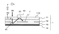
図1は、本発明の太陽電池裏面シートを用いた太陽電池モジュール1に係る一様態を示す断面図である。本発明に係る太陽電池モジュール1は、前面板11と、太陽電池セル12と、封止材13と、裏面シート14を有する。
First, the solar cell back surface sheet | seat which concerns on this invention, and a solar cell module using the same are demonstrated.
FIG. 1 is a cross-sectional view showing a uniform state of a
前面板11は、太陽光や照明光などの光源Lの光を透過するものであり、太陽電池セル12を衝撃、汚れ、水分の浸入等から保護するもので、透過率が高い透明な材料からなる。光源Lの光が太陽光・照明光の側より入射面110に垂直に入射する光H0は、前面板11に入射後、前面板11を透過し、封止材21に入射する。
尚、入射面110の法線NGは、平面P上に前面板11をもっとも安定させた状態で置いた状態における平面Pの法線Nと平行な方向とする。入射面110に垂直に入射する光とは、法線NGに平行に太陽電池モジュール1に入射する光のことである。
The
The normal line NG of the
前面板11の材質は、強化ガラス、サファイアガラス等のガラスあるいは、PC(ポリカーボネート)、PEN(ポリエチレンナフタレート)等の樹脂シートである。前面板11の厚さは強化ガラスであれば約3〜6mm、樹脂シートであれば100μm〜3000μmのものが用いられる。
The material of the
前面板11を射出した光は、封止材12に入射する。封止材12は、太陽電池セル13を固定するものである。前面板11に入射した光H0は、封止材12を透過し、太陽電池セル13へ入射する光H10となり、一部は裏面シート14に入射する光H1となる。封止材12には、入射した光H0を透過させるため光線透過率が高い材料が用いられ、耐熱性、耐高温、耐高湿、耐候性などの耐久性に優れるEVA(エチレン・ビニル・アセテート)が広く使用されている。
The light emitted from the
太陽電池セル13は、光電効果により受光面Jに入射した光を電気へと変換する機能を持ち、単結晶シリコン型、多結晶シリコン型、アモルファスシリコン型、CISG(Cu・In・Ga・Seの化合物)系薄膜型など多くの種類が存在する。太陽電池セル13は、複数個を電極で接続し、モジュールを形成して用いられる。封止材12から太陽電池セル13に入射した光H10は、太陽電池セル13で電気へと変換される。
通常、入射面110に対し斜めに入射した光は、垂直入射の光H0と比較して入射面110で、反射する割合が多く、太陽電池セル13に入射する光が少ない、すなわち発電に利用できる光が少ない。
そのため、入射光H0が、入射面110に垂直に入射するとき、もっとも効率が高い。
The
Usually, the light incident obliquely with respect to the
Therefore, the efficiency is highest when the incident light H0 enters the
裏面シート14は、太陽電池セル13自体を透過した光や、太陽電池セル13に入射せず裏面シートに入射した光H1を反射する機能を有する。
裏面シート14の前面側には散乱要素を含む樹脂層143を有する凹凸構造142、もしくは散乱要素を含む樹脂から構成される凹凸構造142が設けられている。裏面シート14に入射した光H1は、散乱要素で反射される。反射された光H2は前面板11と大気の間等の界面で再度反射され、太陽電池セル13の受光面Jに入射する光H3となり光電変換される。これにより裏面シート14が反射層を有する凹凸構造を持たない構成と比較して光利用効率が向上する効果がある。
The
A concavo-
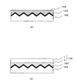
図2は、本発明の裏面シート14の一様態を示す断面図である。本発明に係る裏面シート14は、基材141、凹凸構造142、散乱要素を含む樹脂層143(以下、散乱性反射層143と表記する)からなる。
FIG. 2 is a cross-sectional view showing a uniform state of the
基材141に用いられる材料としては、ポリエチレンテレフタラート、ポリカーボネート、アクリル系樹脂以外にも、耐熱性と透明性を併せ持つポリエステル系樹脂、メタクリル系樹脂、ポリメチルペンテン系樹脂、ポリオレフィン系樹脂、透明ポリイミド、フッ素系樹脂、ポリ乳酸系樹脂、シリコーン、ポリスルフォン系樹脂、ポリエチレンナフタレート系樹脂、ポリエーテルイミド系樹脂、エポキシ樹脂などがある。
In addition to polyethylene terephthalate, polycarbonate, and acrylic resin, materials used for the
基材141は単層であっても多層であってもよく、耐熱性、耐高温、耐高湿、難燃性などの長期耐候性や水蒸気バリア性などの各種性能を付与するために多層構造とすることが望ましい。
The
例えば、最外層には、長期耐候性に優れるPVF(ポリ・フッ化・ビニル)などのフッ素樹脂フィルムやフッ素樹脂塗膜、もしくは低オリゴマーPETフィルムなど耐熱タイプのPETフィルムや耐熱性に優れるPENフィルムなどを配するのが望ましい。 For example, the outermost layer is a fluororesin film such as PVF (poly, fluoride, vinyl), etc. that has excellent long-term weather resistance, a heat-resistant PET film such as a fluororesin coating film, or a low-oligomer PET film, or a PEN film that is excellent in heat resistance It is desirable to arrange etc.
また、例えば、中間層として、水蒸気バリア性に優れるアルミニウム薄膜や、シリカ(SiO2)もしくはアルミナ(Al2O3)蒸着膜などを配するのが望ましい。 For example, it is desirable to arrange an aluminum thin film excellent in water vapor barrier property, a silica (SiO 2 ) or alumina (Al 2 O 3 ) vapor deposition film, etc. as the intermediate layer.
これらのどの組合せを採用するかは、要求性能によって異なるため、必要な性能に合わせて適宜設計するのが望ましい。
例えば、長期耐候性を重視する場合には、最外層としてPVFなどのフッ素樹脂フィルムを用いるのが好ましい。しかし、コストを重視する場合には、耐熱タイプのPETフィルムを用いてもよい。近年では、PETフィルムの耐熱性の改良が進み、十分な長期耐候性が得られる。
また、太陽電池セルとして単結晶シリコンや多結晶シリコンなどの結晶系を用いる場合には、シリカやアルミナ蒸着膜で対応可能であるが、アモルファスシリコンによる薄膜系を用いる場合には、耐湿熱性に劣るため、より水蒸気バリア性に優れるアルミニウム薄膜を用いるのが望ましい。
Which combination to use depends on the required performance, so it is desirable to design appropriately according to the required performance.
For example, when importance is attached to long-term weather resistance, it is preferable to use a fluororesin film such as PVF as the outermost layer. However, when cost is important, a heat-resistant PET film may be used. In recent years, the heat resistance of PET films has been improved and sufficient long-term weather resistance can be obtained.
In addition, when a crystal system such as single crystal silicon or polycrystalline silicon is used as a solar battery cell, silica or alumina deposited film can be used. However, when a thin film system using amorphous silicon is used, it is inferior in heat and moisture resistance. Therefore, it is desirable to use an aluminum thin film that is more excellent in water vapor barrier properties.
凹凸構造142は、基材141の前面側に形成されている。基材141の表面に直接形成してもよく(図2(a))、別の層を設けて形成してもよい(図2(b))。
The
凹凸構造142を基材1に直接形成する方法としては、金型を用いたプレス法・キャスティング法・押し出し成形法・射出成形法などが挙げられる。これらの方法では、シート形成と同時に凹凸構造を形成することが可能である。
Examples of the method for directly forming the concavo-
また、基材141上に別の層を設けて凹凸構造142を形成する方法として、平面スタンパやロールスタンパの凹凸形成面に熱硬化型樹脂、紫外線硬化型樹脂や電子線硬化型樹脂等を塗布または注入し、その上に基材141を配置して、硬化処理後にスタンパから離型するといった方法が挙げられる。これらの方法では、使用する樹脂の粘度を低くすることができるため成形性がよいという利点がある。
In addition, as a method for forming the concavo-
上述の製造方法で使用する樹脂は、特に限定されるものではなく、例えばポリ(メタ)アクリル系樹脂、ポリウレタン系樹脂、フッ素系樹脂、シリコーン系樹脂、ポリイミド系樹脂、エポキシ系樹脂、ポリエチレン系樹脂、ポリプロピレン系樹脂、メタクリル系樹脂、ポリメチルペンテン系樹脂、環状ポリオレフィン系樹脂、アクリロニトリル―(ポリ)スチレン共重合体(AS樹脂)、アクリロニトリル―ブタジエン−スチレン共重合体(ABS樹脂)等のポリスチレン系樹脂、ポリ塩化ビニル系樹脂、ポリカーボネート系樹脂、ポリエステル系樹脂、ポリアミド系樹脂、ポリアミドイミド系樹脂、ポリアリールフタレート系樹脂、ポリスルホン系樹脂、ポリフェニレンスルフィド系樹脂、ポリエーテルスルホン系樹脂、リエチレンナフタレート系樹脂、ポリエーテルイミド系樹脂、アセタール系樹脂、セルロース系樹脂等が挙げられ、これらの樹脂を1種又は2種以上混合して使用することができる。 The resin used in the above-described production method is not particularly limited. For example, poly (meth) acrylic resin, polyurethane resin, fluorine resin, silicone resin, polyimide resin, epoxy resin, polyethylene resin , Polystyrene resins such as polypropylene resins, methacrylic resins, polymethylpentene resins, cyclic polyolefin resins, acrylonitrile- (poly) styrene copolymers (AS resins), acrylonitrile-butadiene-styrene copolymers (ABS resins), etc. Resin, polyvinyl chloride resin, polycarbonate resin, polyester resin, polyamide resin, polyamideimide resin, polyaryl phthalate resin, polysulfone resin, polyphenylene sulfide resin, polyethersulfone resin, polyethylene naphtha Over preparative resin, polyether imide resin, acetal resin, cellulose resin and the like, may be used by mixing these resins singly or in combination.
また、上述の樹脂の他に例えば散乱反射体、硬化剤、可塑剤、分散剤、各種レベリング剤、紫外線吸収剤、抗酸化剤、粘性改質剤、潤滑剤、光安定化剤等の各種添加剤が適宜配合されてもよい。 In addition to the above resins, various additions such as scattering reflectors, curing agents, plasticizers, dispersants, various leveling agents, ultraviolet absorbers, antioxidants, viscosity modifiers, lubricants, light stabilizers, etc. An agent may be appropriately blended.
これら成形法に使用する金型は、バイトによって金属板を切削する方法や、電子ビームによる描画やエッチングによって得られた母型の電鋳加工などにより得られる。 The mold used for these forming methods can be obtained by a method of cutting a metal plate with a cutting tool, or by electroforming a mother die obtained by drawing or etching with an electron beam.
凹凸構造142は、図3(a)〜(d)に示すような、プリズム(a)、多角錐形状(b)、シリンドリカルレンズ(c)、マイクロレンズ(d)、あるいはこれらの逆型のいずれかの形状とするのが望ましい。
The concavo-
これらの構造は、図4に示すような単位構造の底辺Xと高さYのアスペクト比が、0.4以下であることが望ましく、より望ましくは0.35以下である。上述の構造のアスペクト比が0.4より大きい場合には、凹凸構造142を成形するときに金型の先端部分に樹脂が残りやすく成形性が悪い。上述の構造のアスペクト比が0.35以下であれば、樹脂が金型に残る可能性が低くなり、設計通りの形状に成形できる。
In these structures, the aspect ratio of the base X and the height Y of the unit structure as shown in FIG. 4 is desirably 0.4 or less, and more desirably 0.35 or less. When the aspect ratio of the above-described structure is larger than 0.4, the resin tends to remain at the tip portion of the mold when the concavo-
また、上述の構造のアスペクト比は、0.15以上であることが望ましく、より望ましくは0.2以上である。上述の構造のアスペクト比が0.2より小さいと、光利用効率を向上させる効果が弱くなる。上述の構造のアスペクト比が0.15より小さいと、光利用効率を向上させる効果がさらに弱くなる。この理由については後に詳細に説明する。 In addition, the aspect ratio of the above structure is desirably 0.15 or more, and more desirably 0.2 or more. When the aspect ratio of the above structure is smaller than 0.2, the effect of improving the light utilization efficiency is weakened. When the aspect ratio of the above-described structure is smaller than 0.15, the effect of improving the light utilization efficiency is further weakened. The reason for this will be described later in detail.
凹凸構造142は、周期構造を有していてもよく、不定形でもよい。このとき、凹凸構造142の周期のピッチとしては、300μm以下であることが望ましく、より望ましくは、200μm以下である。上述の構造の周期のピッチが300μmより大きい場合には、凹凸構造142を成型するときの凹凸形状の先端部分の型に樹脂が十分に入らないため成型性が悪い。上述の構造の周期のピッチが、200μm以下であれば比較的粘度の高い樹脂でも成型が可能となる。また、上述の構造の周期のピッチが小さすぎると型の作製が難しくなるため、25μm以上であることが望ましく、より望ましくは、50μm以上である。上述の構造の周期のピッチが25μmより小さいと、金型を切削する時間が長くタクトが落ち生産効率が悪い。上述の構造の周期のピッチが50μmより小さいと、凹凸構造142を成形する際に樹脂がうまく溝に入らず凹凸形状の先端部分の形状を金型どおり作製することが困難である。
The
散乱性反射層143は、白色顔料、金属粒子、高屈折率粒子、中空粒子のいずれかの散乱要素を樹脂中に分散させ、凹凸構造142の表面に塗布することにより得られる。
The scattering
散乱要素としては、特に限定されるものではないが、例えば、酸化亜鉛(ZnO)、酸化チタン(TiO2)、酸化アルミニウム(Al2O3)などの白色顔料(金属酸化物)、アルミニウム(Al)ペースト、銀(Ag)ペーストなどの金属粒子、シリカ(Si)などの高屈折率粒子、シリカ(Si)などの中空粒子などを採用することが可能である。このうち、酸化チタン(TiO2)は、屈折率が高く、分散性も得られやすいため好ましい。また、散乱反射体の形状は、球状、針状、板状、鱗片状、破砕状等の任意の粒子形状でよく、特に限定されない。 The scattering element is not particularly limited. For example, white pigment (metal oxide) such as zinc oxide (ZnO), titanium oxide (TiO2), and aluminum oxide (Al2O3), aluminum (Al) paste, silver It is possible to employ metal particles such as (Ag) paste, high refractive index particles such as silica (Si), hollow particles such as silica (Si), and the like. Of these, titanium oxide (TiO2) is preferable because of its high refractive index and easy dispersibility. The shape of the scattering reflector may be any particle shape such as a spherical shape, a needle shape, a plate shape, a scale shape, and a crushed shape, and is not particularly limited.
散乱要素を分散させる樹脂としては、特に限定されるものではなく、例えばポリ(メタ)アクリル系樹脂、ポリウレタン系樹脂、フッ素系樹脂、シリコーン系樹脂、ポリイミド系樹脂、エポキシ系樹脂、ポリエチレン系樹脂、ポリプロピレン系樹脂、メタクリル系樹脂、ポリメチルペンテン系樹脂、環状ポリオレフィン系樹脂、アクリロニトリル―(ポリ)スチレン共重合体(AS樹脂)、アクリロニトリル―ブタジエン―スチレン共重合体(ABS樹脂)等のポリスチレン系樹脂、ポリ塩化ビニル系樹脂、ポリフッ化ビニル系樹脂、ポリカーボネート系樹脂、ポリエステル系樹脂、ポリアミド系樹脂、ポリアミドイミド系樹脂、ポリアリールフタレート系樹脂、ポリスルホン系樹脂、ポリフェニレンスルフィド系樹脂、ポリエーテルスルホン系樹脂、リエチレンナフタレート系樹脂、ポリエーテルイミド系樹脂、アセタール系樹脂、セルロース系樹脂等が挙げられ、これらの樹脂を1種又は2種以上混合して使用することができる。 The resin for dispersing the scattering element is not particularly limited, and for example, poly (meth) acrylic resin, polyurethane resin, fluorine resin, silicone resin, polyimide resin, epoxy resin, polyethylene resin, Polystyrene resins such as polypropylene resin, methacrylic resin, polymethylpentene resin, cyclic polyolefin resin, acrylonitrile- (poly) styrene copolymer (AS resin), acrylonitrile-butadiene-styrene copolymer (ABS resin) , Polyvinyl chloride resin, polyvinyl fluoride resin, polycarbonate resin, polyester resin, polyamide resin, polyamide imide resin, polyaryl phthalate resin, polysulfone resin, polyphenylene sulfide resin, polyether sulfone System resin, triethylene naphthalate resins, polyether imide resins, acetal resins, cellulose resins and the like, may be used by mixing these resins singly or in combination.
散乱性反射層143は、特定の方向へ光を散乱反射させるために、凹凸構造142に追従する形状に設けることが望ましい、すなわち、樹脂層143を形成したのちも凹凸構造142の形状が保たれていることが望ましい(図5(a))。凹凸構造142の形状が保たれていない場合(図5(b))、特定の方向へ光が反射する機能がなくなり、等方散乱となってしまう。
The scattering
図6は、本発明の裏面シート14の別の一様態を示す断面図である。本発明に係る裏面シート14は、基材141、散乱要素を含む樹脂から構成される凹凸構造142(以下、散乱性凹凸構造142と表記する)からなる。
FIG. 6 is a cross-sectional view showing another embodiment of the
図6に示す裏面シート14は、散乱要素を含む樹脂層(散乱性反射層)143を設けない、散乱要素を含む樹脂から構成される凹凸構造(散乱性凹凸構造)142を設ける、の2点でのみ図2に示す裏面シート14と異なっている。
The
図6に示す裏面シート14に用いる基材141としては、図2に示す裏面シート14と同様の材料、構成を採用可能であり、単層であっても多層であってもよく、耐熱性、耐高温、耐高湿、難燃性などの長期耐候性や水蒸気バリア性などの各種性能を付与するために多層構造とすることが望ましい。図2に示す裏面シート14について説明したのと同様の各種構成を採用可能であり、要求性能に合わせて適宜設計するのが望ましい。
As the
散乱性凹凸構造142は、基材141の前面側に形成されている。基材141の表面に直接形成してもよく(図6(a))、別の層を設けて形成してもよい(図6(b))。
The scattering
散乱性凹凸構造142を基材141に直接形成する方法、及び基材141上に別の層を設けて散乱性凹凸構造142を形成する方法としては、図2に示す裏面シート14について説明したのと同様の各種製法を採用可能である。
As the method for directly forming the scattering
上述の製造方法で使用する樹脂は、特に限定されるものではなく、図2に示す裏面シート142について説明したのと同様の各種樹脂材料を採用可能である。
The resin used in the above manufacturing method is not particularly limited, and various resin materials similar to those described for the
また、上述の樹脂の他に、図2に示す裏面シート142について説明したのと同様の各種添加剤を適宜配合してもよい。
Moreover, you may mix | blend suitably the various additives similar to having demonstrated the
散乱性凹凸構造142は、凹凸構造を構成する樹脂に、白色顔料、金属粒子、高屈折率粒子、中空粒子のいずれかの散乱要素を分散させることにより得られる。
The scattering concavo-
散乱要素としては、特に限定されるものではないが、図2に示す裏面シート142について説明したのと同様の各種材料、形状を採用可能である。
Although it does not specifically limit as a scattering element, Various materials and shapes similar to having demonstrated the
散乱性凹凸構造142は、図2に示す裏面シート14について説明したのと同様に、図3(a)〜(d)に示すような、プリズム、多角錐形状、シリンドリカルレンズ、マイクロレンズ、あるいはこれらの逆型のいずれかの形状とするのが望ましい。
The scattering concavo-
これらの構造は、図2に示す裏面シート14について説明したのと同様の理由で、図4に示すような単位構造の底辺Xと高さYのアスペクト比が、0.4以下であることが望ましく、より望ましくは0.35以下である。
In these structures, the aspect ratio between the base X and the height Y of the unit structure as shown in FIG. 4 is 0.4 or less for the same reason as described for the
また、上述の構造のアスペクト比は、図2に示す裏面シート14について説明したのと同様の理由で、0.15以上であることが望ましく、より望ましくは0.2以上である。
In addition, the aspect ratio of the above-described structure is desirably 0.15 or more, and more desirably 0.2 or more, for the same reason as described for the
散乱性凹凸構造142は、周期構造を有していてもよく、不定形でもよい。このとき、図2に示す裏面シート14について説明したのと同様の理由で、凹凸構造142の周期のピッチとしては、300μm以下であることが望ましく、より望ましくは、200μm以下である。また、25μm以上であることが望ましく、より望ましくは、50μm以上である。
The scattering
図2及び図6に示す裏面シート14は、トップコート層144をさらに備えていてもよい。このとき、トップコート層144は、電気絶縁性を有する材料であることが望ましい。
The
太陽電池裏面シートに求められる重要な性能の一つとして、電気絶縁性がある。電気絶縁性は、太陽電池が内部に電極を含むモジュールであることから、長期使用での漏電などを防ぐために必ず必要な性能であり、特に、セル側の表面が電気絶縁性であることが求められている。 One of the important performances required for the solar cell back sheet is electrical insulation. Since electrical insulation is a module that includes an electrode inside the solar cell, it is a necessary performance to prevent leakage during long-term use. In particular, the cell-side surface must be electrically insulating. It has been.
電気絶縁性を示す数値基準の一つとして、絶縁破壊電圧がある。絶縁破壊電圧は、絶縁破壊電圧以上の電圧が加わると絶縁状態が破壊される、という指標であり、絶縁破壊電圧が高い方が電気的に安定であると言える。 One of numerical standards indicating electrical insulation is a breakdown voltage. The breakdown voltage is an index that the insulation state is broken when a voltage higher than the breakdown voltage is applied, and it can be said that the higher breakdown voltage is electrically stable.
一般的に、裏面シートのセル側の表面(最内面)には、電気絶縁用プラスチックフィルム、もしくはPVF(ポリ・フッ化・ビニル)などのフッ素樹脂フィルムやフッ素樹脂塗膜が配されている。
例えば、参考文献1(「太陽光発電システム構成材料」(工業調査会))によると、各種電気絶縁用プラスチックフィルム(25μm)の絶縁破壊電圧(KV)のおおよその数値は、PET(ポリエチレンテレフタレート) 6.5、PEN(ポリエチレンナフタレート) 7.5、PVC(延伸硬質塩ビ) 4.0、PC(ポリカーボネート) 5.0、OPP(延伸ポリプロピレン) 6.0、PE(ポリエチレン) 4.0、TAC(トリアセテート) 3.0、PI(ポリイミド) 7.0である。これらはいずれも絶縁材料としての絶縁破壊電圧を満たしている(参考 JISC2318/電気用二軸配向ポリエチレンテレフタレートフィルム)。
また、PVF(ポリ・フッ化・ビニル)の代表的な製品であるデュポン社のテドラーの絶縁破壊電圧は、約3.0KVである。
これらの各種材料、特に電気絶縁用PET及びPVFは、電気絶縁材料として太陽電池裏面シートへの使用実績があり、要求性能を満たすことが確認されている。
以上より、絶縁破壊電圧は3.0KV以上であるのが望ましい。絶縁破壊電圧が2.0KV以下の場合、長期使用による漏電の可能性が高くなる。
In general, a plastic film for electrical insulation, or a fluororesin film such as PVF (poly, fluoride, vinyl) or a fluororesin coating film is disposed on the cell side surface (innermost inner surface) of the back sheet.
For example, according to Reference 1 (“Photovoltaic power generation system constituent material” (Industry Research Committee)), the approximate value of the dielectric breakdown voltage (KV) of various plastic films for electrical insulation (25 μm) is PET (polyethylene terephthalate). 6.5, PEN (polyethylene naphthalate) 7.5, PVC (stretched hard vinyl chloride) 4.0, PC (polycarbonate) 5.0, OPP (stretched polypropylene) 6.0, PE (polyethylene) 4.0, TAC (Triacetate) 3.0 and PI (polyimide) 7.0. All of these satisfy the dielectric breakdown voltage as an insulating material (reference JISC2318 / biaxially oriented polyethylene terephthalate film for electrical use).
The dielectric breakdown voltage of a DuPont Tedlar, which is a typical PVF (poly, fluoride, vinyl) product, is about 3.0 KV.
These various materials, particularly PET and PVF for electrical insulation, have been used for solar cell back sheets as electrical insulation materials, and have been confirmed to satisfy the required performance.
From the above, it is desirable that the dielectric breakdown voltage is 3.0 KV or more. When the dielectric breakdown voltage is 2.0 KV or less, the possibility of leakage due to long-term use increases.
上述の電気絶縁性トップコート層144は、上述の各種材料を図2及び図6に示す裏面シート14上に塗布することで得られる。このとき、使用する材料は透明あるいは半透明性の材料であることが好ましい。
また、用いる材料としては、上記に限ったものではなく、絶縁破壊電圧の基準値を満たす材料であれば、適宜採用することが可能である。
The above-mentioned electrically insulating
In addition, the material to be used is not limited to the above, and any material that satisfies the reference value of the dielectric breakdown voltage can be used as appropriate.
なお、トップコート層144は、単層でもよく多層でもよい。例えば、電気絶縁性を有する材料を直接塗布する単層構成とすることができる(図7(a))。
また、例えば、上述の電気絶縁性プラスチックフィルムfを接着層aを介して貼合する多層構成としても良い(図7(b))。中でも、同時に要求される耐熱性、耐湿性、機械強度などにも優れ、コスト面でも有利である電気絶縁性PETフィルムが特に好ましい。
これら構成は、要求される特性によって、使用する材料が異なり、構成も異なるため、要求特性に応じて適宜設計するのが望ましい。
The
For example, it is good also as a multilayer structure which bonds the above-mentioned electrically insulating plastic film f through the contact bonding layer a (FIG.7 (b)). Among them, an electrically insulating PET film that is excellent in heat resistance, moisture resistance, mechanical strength, and the like that are simultaneously required and advantageous in terms of cost is particularly preferable.
Since these materials use different materials and have different structures depending on required characteristics, it is desirable to design them appropriately according to the required characteristics.
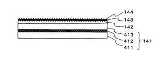
図8に、裏面シート14の層構成の例を示す。
基材141は、耐熱性PETフィルム411、水蒸気バリア性を得るためのシリカ蒸着層412、シリカ蒸着層を保護するPETフィルム413からなる。基材141上には、凹凸構造142を形成する樹脂層が配置されている。凹凸構造142上には、散乱要素を含む樹脂層143が形成されている。
In FIG. 8, the example of a laminated constitution of the
The
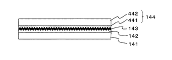
図9に、裏面シート14の別の層構成の例を示す。
基材141は、長期耐候性を得るためのPVF層411、耐熱性PETフィルム412、接着層413、高い水蒸気バリア性を得るためのアルミニウム箔層414、接着層415、表面に凹凸構造142が一体成形されたPETフィルム416からなる。基材141上の凹凸構造142上には、散乱要素を含む樹脂層143が形成されている。散乱要素を含む樹脂層143上には、接着層441、電気絶縁性を得るための電気絶縁性PETフィルム442からなるトップコート層144が配置されている。
In FIG. 9, the example of another layer structure of the
The
図10に、裏面シート14のさらに別の層構成の例を示す。
基材141は、長期耐候性を得るためのPVF層411、耐熱性PETフィルム412、水蒸気バリア性を得るためのシリカ蒸着層413、シリカ蒸着層を保護し、かつ表面に凹凸構造142が一体成形されたPETフィルム414からなる。基材141上には散乱要素を含む樹脂により凹凸構造142が形成されている。凹凸構造142上には、長期耐候性をより強化し、かつ電気絶縁性を得るためのPVF層からなるトップコート層144が配置されている。
In FIG. 10, the example of another layer structure of the
The
図11に、裏面シート14のさらに別の層構成の例を示す。
基材141は、長期耐候性を得るためのPVF層411、耐熱性PETフィルム412、水蒸気バリア性を得るためのシリカ蒸着層413、シリカ蒸着層を保護するPETフィルム414、長期耐候性をより強化するためのPVF層415、接着層416、表面に凹凸構造142が一体成形され、かつ散乱要素を含む樹脂から成るフィルム417からなる。凹凸構造142上には、接着層441、電気絶縁性を得るための電気絶縁性PETフィルム442からなるトップコート層144が配置されている。
In FIG. 11, the example of another layer structure of the
The
裏面シート14の層構成は、例示した層構成に限るものではなく、例示した層構成以外にも、要求特性に応じて様々な変形が可能である。
The layer configuration of the
次に、裏面シート14による光利用効率の向上の手法について説明する。
Next, a method for improving the light utilization efficiency by the
図12は図2に示す裏面シート14に入射した光が、散乱性反射層143を有する凹凸構造142によって反射され、太陽電池セル12の受光面Jに入射する機構を示した概略図である(層構成の詳細は図示せず)。なお、ここでは凹凸構造としてプリズムを採用している。
裏面シート14の前面側には散乱性反射層143を有する凹凸構造142が設けられている。裏面シート14に入射した光H1は、散乱性反射層143で反射される。反射された光はH2を中心に広がりを持つ。H2を中心とする反射光は前面板11と大気の間等の界面で再度反射され、太陽電池セル13の受光面Jに入射する光H3となり光電変換される。太陽電池セル13の受光面Jに入射する光H3が増えれば、光電変換量が増え、光利用効率の向上が見込める。
FIG. 12 is a schematic view showing a mechanism in which the light incident on the
An
図12(c)にプリズムの頂角θと反射角α(入射角α)の関係を示す。ここで、入射面110に対して垂直に光が入射した場合には、頂角θと反射角αの間には以下の関係が成り立つ。

散乱性反射層143で反射した光は、反射角αで反射するH2を中心に広がりを持った光となる。
The light reflected by the scattering
散乱性反射層143で反射した光の中心成分H2は、前面板11と大気の界面で反射する。このときの入射光H2の入射角は2αである。
このとき、2αが臨界角φ以上の場合には、前面板と大気の界面で全反射するため、入射光H2はロスが極めて少なく反射光H3となる(図11(a))。一方、2αが臨界角φより小さい場合には、反射光H3の他に、透過光H4が発生する(図11(b))。透過光H4の発生によって反射光H3の光量が減少する、すなわち太陽電池セル12の受光面Jに入射する光H3の光量が減少するため、入射光H2の入射角2αが臨界角φ以上となることが望ましい。
The central component H2 of the light reflected by the scattering
At this time, when 2α is equal to or larger than the critical angle φ, the light is totally reflected at the interface between the front plate and the atmosphere, so that the incident light H2 is very little loss and becomes reflected light H3 (FIG. 11A). On the other hand, when 2α is smaller than the critical angle φ, transmitted light H4 is generated in addition to the reflected light H3 (FIG. 11B). Since the amount of reflected light H3 decreases due to the generation of transmitted light H4, that is, the amount of light H3 incident on the light receiving surface J of the
臨界角φは、この場合には前面板11の屈折率n1と大気の屈折率n2によって決まり、以下の関係が成り立つ。
例えば、前面板11に強化ガラスなどのガラスを用いた場合には、屈折率n1は約1.5、大気の屈折率n2は約1.0であるため、臨界角φは約42°となる。
散乱性反射層143での反射光H2を有効に利用するためには、2αが臨界角φ以上となることが望ましい、すなわち、臨界角φが42°のときには散乱性反射層143での反射角αが21°以上であることが望ましい。
For example, in the case of using a glass such as tempered glass on the
In order to effectively use the reflected light H2 from the
散乱性反射層143で反射した光は広がりを持つため、中心成分H2の反射角αが21°以上であっても、前面板11と大気の界面への入射角2αが臨界角φ以下となる成分が存在する。この成分は、透過光H4となりロスとなる。ただし、こまでは、前面板11の入射面110への入射角が0°である場合を考えてきたが、実際には、入射する光の入射角は様々である。そのため、正面からの光に対してはロスとなる成分が発生するとしても、入射角が変わったときには逆に有効に利用できる成分が多くなる場合がある。
Since the light reflected by the
ここで、プリズムの底辺Xと高さYのアスペクト比に対する、頂角θ及び反射層143での反射角αのおおよその値を下記の表1に示す。
以上のことを考慮すると、プリズムのアスペクト比は、0.2以上であることが望ましい。しかし、実際には、反射層143に入射する光の入射角は様々であるので、アスペクト比が0.15以上であれば、最終的に受光面Jに入射する光は発生する。しかし、アスペクト比が0.15以下になると、反射層143で反射され、前面板11と大気の界面に入射する光H2の入射角2αが臨界角よりも10°近く小さくなり、全反射する光が少なくなる。
Considering the above, it is desirable that the aspect ratio of the prism is 0.2 or more. However, actually, since the incident angle of the light incident on the
なお、既述の通り、プリズムのアスペクト比が0.4以上であると成形性が悪くなるためアスペクト比は、0.4以下であることが望ましく、0.35以下であればさらに成形性がよくなるため、より望ましくは0.35以下である。 As described above, when the aspect ratio of the prism is 0.4 or more, the moldability deteriorates. Therefore, the aspect ratio is desirably 0.4 or less, and if the aspect ratio is 0.35 or less, the moldability is further improved. In order to improve, it is more desirably 0.35 or less.
図13に示すような、PETフィルムからなる基材141、紫外線硬化性樹脂からなる凹凸構造142、散乱性反射層143、及び接着層441、PETフィルム442からなるトップコート層144からなる裏面シート14を作製し、光利用効率の向上の効果を確認した。このとき、凹凸構造142としてアスペクト比0.2、ピッチ200μmのプリズムを採用した。
図12に示すような位置関係において、太陽電池セル12にあたる部分に光センサーを配置して光量を測定したところ、凹凸構造及び反射層がないときの光量を1とすると、図13に示す裏面シートを用いた場合の光量は相対比で1.2となった。これにより、反射層143を有する凹凸構造142を裏面シートの前面側に設けると、太陽電池モジュールの光利用効率の向上が可能であることが確認できた。
As shown in FIG. 13, a
In the positional relationship as shown in FIG. 12, when the light amount was measured by arranging a photosensor in the portion corresponding to the
また、図13に示す裏面シート14からトップコート層144を省いた構成の裏面シート14(図示せず)を作製し、同様の測定を行ったところ、トップコート層144がある場合と同じ結果が得られた。これにより、トップコート層144は光利用効率の向上を阻害するものではないことが確認できた。
Moreover, when the back sheet 14 (not shown) of the structure which excluded the
また、本発明の裏面シート14は、太陽電池モジュールへの使用に限るものではなく、LED照明やEL素子などの発光素子の光利用効率向上など、光利用効率向上が望まれる光学素子やディスプレイ部材への転用が可能である。
Further, the
1…太陽電池モジュール、11…前面板、12…太陽電池セル、13…封止材、14…裏面シート、141…基材、142…凹凸構造、143…反射層、144…トップコート層、110…入射面、F…光源方向、J…受光面、N…法線、NG…前面板11の法線、H0…太陽電池モジュールに垂直に入射する光、H1…反射層に入射する光、H2…反射光の中心成分、H3…再利用される光、L…光源、X…凹凸構造の底辺、Y…凹凸構造の高さ、e…電気絶縁性の層、f…電気絶縁性フィルム、a…接着層、411、412、413、414、415、416、417…基材141を構成する層、441、442…トップコート層144を構成する層、θ…プリズムの頂角、α…反射角、β…透過角、φ…臨界角
441、442、443…トップコート層144を構成する層、θ…プリズムの頂角、α…反射角、β…透過角、φ…臨界角
DESCRIPTION OF
Claims (12)
前記裏面シートの前面側に光散乱反射機能を有する凹凸構造が形成されていることを特徴とする太陽電池裏面シート。 In a solar cell module having at least a translucent front plate, solar cells, a sealing material, and a back sheet,
An uneven structure having a light scattering reflection function is formed on the front side of the back sheet.
Priority Applications (1)
| Application Number | Priority Date | Filing Date | Title |
|---|---|---|---|
| JP2008295373A JP2010123720A (en) | 2008-11-19 | 2008-11-19 | Solar cell backside sheet and solar cell module |
Applications Claiming Priority (1)
| Application Number | Priority Date | Filing Date | Title |
|---|---|---|---|
| JP2008295373A JP2010123720A (en) | 2008-11-19 | 2008-11-19 | Solar cell backside sheet and solar cell module |
Publications (1)
| Publication Number | Publication Date |
|---|---|
| JP2010123720A true JP2010123720A (en) | 2010-06-03 |
Family
ID=42324808
Family Applications (1)
| Application Number | Title | Priority Date | Filing Date |
|---|---|---|---|
| JP2008295373A Withdrawn JP2010123720A (en) | 2008-11-19 | 2008-11-19 | Solar cell backside sheet and solar cell module |
Country Status (1)
| Country | Link |
|---|---|
| JP (1) | JP2010123720A (en) |
Cited By (4)
| Publication number | Priority date | Publication date | Assignee | Title |
|---|---|---|---|---|
| JP2013149879A (en) * | 2012-01-23 | 2013-08-01 | Toyota Body Research & Development Co Ltd | Photovoltaic power generation system |
| JP2016072540A (en) * | 2014-09-30 | 2016-05-09 | 大日本印刷株式会社 | Rear surface protective sheet and solar cell module using the same |
| JP2016127220A (en) * | 2015-01-08 | 2016-07-11 | 大日本印刷株式会社 | Rear surface protective sheet for solar cell module and solar cell module using the same |
| JP2016183456A (en) * | 2015-03-25 | 2016-10-20 | 富士通株式会社 | Solar power generation device, sensing device and information processing system |
-
2008
- 2008-11-19 JP JP2008295373A patent/JP2010123720A/en not_active Withdrawn
Cited By (4)
| Publication number | Priority date | Publication date | Assignee | Title |
|---|---|---|---|---|
| JP2013149879A (en) * | 2012-01-23 | 2013-08-01 | Toyota Body Research & Development Co Ltd | Photovoltaic power generation system |
| JP2016072540A (en) * | 2014-09-30 | 2016-05-09 | 大日本印刷株式会社 | Rear surface protective sheet and solar cell module using the same |
| JP2016127220A (en) * | 2015-01-08 | 2016-07-11 | 大日本印刷株式会社 | Rear surface protective sheet for solar cell module and solar cell module using the same |
| JP2016183456A (en) * | 2015-03-25 | 2016-10-20 | 富士通株式会社 | Solar power generation device, sensing device and information processing system |
Similar Documents
| Publication | Publication Date | Title |
|---|---|---|
| TWI514598B (en) | Photoelectric conversion device and method for manufacturing the same | |
| US20090114279A1 (en) | Solar cell sheet and a method for the preparation of the same | |
| JP4404753B2 (en) | Solar cell module | |
| WO2005081324A1 (en) | Substrate for photoelectric converter, photoelectric converter, and multilayer photoelectric converter | |
| EP2346092B1 (en) | Photoelectric module | |
| JP2011108725A (en) | Back sheet, solar battery back sheet, and solar battery module using the same | |
| US20090293934A1 (en) | Photoelectric Conversion Device | |
| US20140209155A1 (en) | Three-Dimensional Metamaterial Device with Photovoltaic Bristles | |
| JP2014042018A (en) | Sunlight lighting system | |
| JP2010123720A (en) | Solar cell backside sheet and solar cell module | |
| JP2010123719A (en) | Solar cell backside sheet and solar cell module | |
| JP2011029273A (en) | Solar cell module | |
| JP5729086B2 (en) | Solar cell module | |
| US20180366605A1 (en) | Solar power sunroof device having low reflectance and manufacturing method thereof | |
| JP2012204460A (en) | Solar battery backside sheet and solar battery module using the same | |
| JP2010287715A (en) | Thin film solar cell and method of manufacturing the same | |
| JP2013115216A (en) | Solar cell backside sheet and solar cell module | |
| JP5304444B2 (en) | Solar cell back sheet and solar cell module using the same | |
| JP2009094501A (en) | Photoelectric conversion device | |
| JP2008277423A (en) | Photoelectric conversion device | |
| JP2008053273A (en) | Solar cell and its manufacturing method | |
| JP4969337B2 (en) | Photoelectric conversion device | |
| JP2014236123A (en) | Solar battery module and method for manufacturing the same | |
| JP2013004948A (en) | Solar cell module | |
| JPH11298020A (en) | Thin-film solar cell module |
Legal Events
| Date | Code | Title | Description |
|---|---|---|---|
| A621 | Written request for application examination |
Free format text: JAPANESE INTERMEDIATE CODE: A621 Effective date: 20111021 |
|
| A761 | Written withdrawal of application |
Free format text: JAPANESE INTERMEDIATE CODE: A761 Effective date: 20120903 |