JP2010117161A - 検査装置 - Google Patents
検査装置 Download PDFInfo
- Publication number
- JP2010117161A JP2010117161A JP2008288794A JP2008288794A JP2010117161A JP 2010117161 A JP2010117161 A JP 2010117161A JP 2008288794 A JP2008288794 A JP 2008288794A JP 2008288794 A JP2008288794 A JP 2008288794A JP 2010117161 A JP2010117161 A JP 2010117161A
- Authority
- JP
- Japan
- Prior art keywords
- film thickness
- thickness distribution
- unit
- substrate
- inspection apparatus
- Prior art date
- Legal status (The legal status is an assumption and is not a legal conclusion. Google has not performed a legal analysis and makes no representation as to the accuracy of the status listed.)
- Pending
Links
Images


Landscapes
- Length Measuring Devices By Optical Means (AREA)
Priority Applications (1)
| Application Number | Priority Date | Filing Date | Title |
|---|---|---|---|
| JP2008288794A JP2010117161A (ja) | 2008-11-11 | 2008-11-11 | 検査装置 |
Applications Claiming Priority (1)
| Application Number | Priority Date | Filing Date | Title |
|---|---|---|---|
| JP2008288794A JP2010117161A (ja) | 2008-11-11 | 2008-11-11 | 検査装置 |
Publications (2)
| Publication Number | Publication Date |
|---|---|
| JP2010117161A true JP2010117161A (ja) | 2010-05-27 |
| JP2010117161A5 JP2010117161A5 (enExample) | 2012-07-12 |
Family
ID=42304938
Family Applications (1)
| Application Number | Title | Priority Date | Filing Date |
|---|---|---|---|
| JP2008288794A Pending JP2010117161A (ja) | 2008-11-11 | 2008-11-11 | 検査装置 |
Country Status (1)
| Country | Link |
|---|---|
| JP (1) | JP2010117161A (enExample) |
Cited By (6)
| Publication number | Priority date | Publication date | Assignee | Title |
|---|---|---|---|---|
| US9036895B2 (en) | 2012-05-10 | 2015-05-19 | Samsung Electronics Co., Ltd. | Method of inspecting wafer |
| JPWO2020250868A1 (enExample) * | 2019-06-10 | 2020-12-17 | ||
| CN114659451A (zh) * | 2020-12-22 | 2022-06-24 | 松山湖材料实验室 | 膜厚测量方法及测量装置 |
| JP2022179471A (ja) * | 2021-05-21 | 2022-12-02 | 浜松ホトニクス株式会社 | 膜厚測定装置及び膜厚測定方法 |
| EP4431867A1 (de) * | 2023-03-17 | 2024-09-18 | Confovis GmbH | Verfahren zum erstellen eines schichtdickenvariationsprofils einer oberflächenschicht eines substrates |
| JP7788358B2 (ja) | 2021-05-21 | 2025-12-18 | 浜松ホトニクス株式会社 | 膜厚測定装置及び膜厚測定方法 |
Citations (7)
| Publication number | Priority date | Publication date | Assignee | Title |
|---|---|---|---|---|
| JPS61182507A (ja) * | 1985-02-08 | 1986-08-15 | Nec Kansai Ltd | 膜厚測定装置 |
| JPS6457107A (en) * | 1987-08-28 | 1989-03-03 | Hitachi Ltd | Measuring method of distribution of film thickness and apparatus therefor |
| JPH1047926A (ja) * | 1996-08-07 | 1998-02-20 | Dainippon Screen Mfg Co Ltd | 膜厚測定装置および膜厚測定方法 |
| JP2001091222A (ja) * | 1999-09-17 | 2001-04-06 | Dainippon Screen Mfg Co Ltd | 膜厚測定装置の校正方法および膜厚測定装置および校正用部材 |
| JP2002039718A (ja) * | 2000-07-19 | 2002-02-06 | Olympus Optical Co Ltd | 薄膜の合否判定方法および装置 |
| JP2005221401A (ja) * | 2004-02-06 | 2005-08-18 | Dainippon Printing Co Ltd | 膜厚測定方法および装置 |
| JP2008139065A (ja) * | 2006-11-30 | 2008-06-19 | Nikon Corp | 膜評価装置及び膜評価方法 |
-
2008
- 2008-11-11 JP JP2008288794A patent/JP2010117161A/ja active Pending
Patent Citations (7)
| Publication number | Priority date | Publication date | Assignee | Title |
|---|---|---|---|---|
| JPS61182507A (ja) * | 1985-02-08 | 1986-08-15 | Nec Kansai Ltd | 膜厚測定装置 |
| JPS6457107A (en) * | 1987-08-28 | 1989-03-03 | Hitachi Ltd | Measuring method of distribution of film thickness and apparatus therefor |
| JPH1047926A (ja) * | 1996-08-07 | 1998-02-20 | Dainippon Screen Mfg Co Ltd | 膜厚測定装置および膜厚測定方法 |
| JP2001091222A (ja) * | 1999-09-17 | 2001-04-06 | Dainippon Screen Mfg Co Ltd | 膜厚測定装置の校正方法および膜厚測定装置および校正用部材 |
| JP2002039718A (ja) * | 2000-07-19 | 2002-02-06 | Olympus Optical Co Ltd | 薄膜の合否判定方法および装置 |
| JP2005221401A (ja) * | 2004-02-06 | 2005-08-18 | Dainippon Printing Co Ltd | 膜厚測定方法および装置 |
| JP2008139065A (ja) * | 2006-11-30 | 2008-06-19 | Nikon Corp | 膜評価装置及び膜評価方法 |
Cited By (13)
| Publication number | Priority date | Publication date | Assignee | Title |
|---|---|---|---|---|
| US9036895B2 (en) | 2012-05-10 | 2015-05-19 | Samsung Electronics Co., Ltd. | Method of inspecting wafer |
| CN113994199B (zh) * | 2019-06-10 | 2024-10-18 | 东京毅力科创株式会社 | 基板处理装置、基板检查方法和存储介质 |
| JPWO2020250868A1 (enExample) * | 2019-06-10 | 2020-12-17 | ||
| WO2020250868A1 (ja) * | 2019-06-10 | 2020-12-17 | 東京エレクトロン株式会社 | 基板処理装置、基板検査方法、及び記憶媒体 |
| CN113994199A (zh) * | 2019-06-10 | 2022-01-28 | 东京毅力科创株式会社 | 基板处理装置、基板检查方法和存储介质 |
| US20220252507A1 (en) * | 2019-06-10 | 2022-08-11 | Tokyo Electron Limited | Substrate processing apparatus, substrate inspecting method, and storage medium |
| JP7282171B2 (ja) | 2019-06-10 | 2023-05-26 | 東京エレクトロン株式会社 | 基板処理装置、基板検査方法、及び記憶媒体 |
| TWI848121B (zh) * | 2019-06-10 | 2024-07-11 | 日商東京威力科創股份有限公司 | 基板處理裝置、基板檢查方法及記錄媒體 |
| CN114659451A (zh) * | 2020-12-22 | 2022-06-24 | 松山湖材料实验室 | 膜厚测量方法及测量装置 |
| CN114659451B (zh) * | 2020-12-22 | 2025-01-28 | 松山湖材料实验室 | 膜厚测量方法及测量装置 |
| JP2022179471A (ja) * | 2021-05-21 | 2022-12-02 | 浜松ホトニクス株式会社 | 膜厚測定装置及び膜厚測定方法 |
| JP7788358B2 (ja) | 2021-05-21 | 2025-12-18 | 浜松ホトニクス株式会社 | 膜厚測定装置及び膜厚測定方法 |
| EP4431867A1 (de) * | 2023-03-17 | 2024-09-18 | Confovis GmbH | Verfahren zum erstellen eines schichtdickenvariationsprofils einer oberflächenschicht eines substrates |
Similar Documents
| Publication | Publication Date | Title |
|---|---|---|
| JP5790644B2 (ja) | 検査装置および検査方法 | |
| KR101261047B1 (ko) | 표면 검사장치, 표면 검사방법 및 노광 시스템 | |
| TWI690006B (zh) | 用於模型化基礎臨界尺寸測量之技術及系統 | |
| TWI587082B (zh) | Mask inspection device, mask evaluation method and mask evaluation system | |
| US20190304851A1 (en) | Sample inspection using topography | |
| JP4460659B2 (ja) | 薄膜の膜厚計測方法及びその装置並びにそれを用いた薄膜デバイスの製造方法及びその製造装置 | |
| TWI592654B (zh) | Inspection equipment and inspection methods | |
| US20110071784A1 (en) | Goos-Hanchen compensation in autofocus systems | |
| US10803576B2 (en) | Defect inspection apparatus and defect inspection method | |
| CN113330550B (zh) | 叠对计量系统和方法 | |
| CN113330299B (zh) | 成像反射计 | |
| TW201418661A (zh) | 在角度解析反射量測中之掃描及演算地消除來自光學量測之繞射 | |
| WO2008007614A1 (en) | Surface inspecting apparatus | |
| KR101994524B1 (ko) | 포커싱 장치, 포커싱 방법 및 패턴 검사 방법 | |
| WO2013081072A1 (ja) | 測定装置、測定方法および半導体デバイス製造方法 | |
| US10282635B2 (en) | Pattern inspection apparatus | |
| JP2004012301A (ja) | パターン欠陥検出方法およびその装置 | |
| US7528954B2 (en) | Method of adjusting optical imaging system, positional deviation detecting mark, method of detecting positional deviation, method of detecting position, position detecting device and mark identifying device | |
| CN111801622B (zh) | 使用多个波长的叠加测量 | |
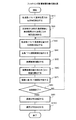
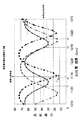
| JP2010117161A (ja) | 検査装置 | |
| JP2010048604A (ja) | 膜厚測定装置および膜厚測定方法 | |
| TW200839916A (en) | Polarization imaging | |
| JP2011174764A (ja) | 検査方法および検査装置 | |
| US10067028B2 (en) | Calibration structure and calibration method for calibrating optical measuring devices | |
| JP7017475B2 (ja) | フォトマスクブランク関連基板の表面状態の評価方法 |
Legal Events
| Date | Code | Title | Description |
|---|---|---|---|
| A621 | Written request for application examination |
Free format text: JAPANESE INTERMEDIATE CODE: A621 Effective date: 20111110 |
|
| A521 | Written amendment |
Free format text: JAPANESE INTERMEDIATE CODE: A523 Effective date: 20111124 |
|
| A521 | Written amendment |
Free format text: JAPANESE INTERMEDIATE CODE: A523 Effective date: 20120524 |
|
| A977 | Report on retrieval |
Free format text: JAPANESE INTERMEDIATE CODE: A971007 Effective date: 20121221 |
|
| A131 | Notification of reasons for refusal |
Free format text: JAPANESE INTERMEDIATE CODE: A131 Effective date: 20130108 |
|
| A521 | Written amendment |
Free format text: JAPANESE INTERMEDIATE CODE: A523 Effective date: 20130311 |
|
| A02 | Decision of refusal |
Free format text: JAPANESE INTERMEDIATE CODE: A02 Effective date: 20140311 |