JP2010104146A - Power converting apparatus - Google Patents
Power converting apparatus Download PDFInfo
- Publication number
- JP2010104146A JP2010104146A JP2008273238A JP2008273238A JP2010104146A JP 2010104146 A JP2010104146 A JP 2010104146A JP 2008273238 A JP2008273238 A JP 2008273238A JP 2008273238 A JP2008273238 A JP 2008273238A JP 2010104146 A JP2010104146 A JP 2010104146A
- Authority
- JP
- Japan
- Prior art keywords
- noise filter
- circuit board
- filter circuit
- base portion
- opening
- Prior art date
- Legal status (The legal status is an assumption and is not a legal conclusion. Google has not performed a legal analysis and makes no representation as to the accuracy of the status listed.)
- Withdrawn
Links
Images


Abstract
Description
本発明は、ノイズフィルタ回路を内蔵した電力変換装置に関する。 The present invention relates to a power conversion device incorporating a noise filter circuit.
周知のように電力変換装置は可変周波数・可変電圧を出力する機能を有する。この機能はIGBT等の主回路素子からなる主回路モジュールにおいて、主回路素子を高速にスイッチング動作させることで実現している。また、主回路素子の高速スイッチング動作は伝導ノイズを発生させることも一般に知られている。この伝導ノイズは電力変換装置の入出力配線や電力変換装置が設置された金属盤などの導体を介して他機器に伝わり、他機器を誤作動させる可能性がある。よって、他機器の誤作動回避を目的として伝導ノイズを低減することがある。また、海外では伝導ノイズの許容値が定められており、この許容値以下に伝導ノイズを低減することが電力変換装置を製品化できる条件となっている。 As is well known, the power converter has a function of outputting a variable frequency and a variable voltage. This function is realized by switching the main circuit element at high speed in a main circuit module composed of main circuit elements such as IGBT. It is also generally known that high-speed switching operation of the main circuit element generates conduction noise. This conduction noise is transmitted to other devices via conductors such as input / output wiring of the power conversion device and a metal board on which the power conversion device is installed, and may cause other devices to malfunction. Therefore, conduction noise may be reduced for the purpose of avoiding malfunction of other equipment. In addition, an allowable value of conduction noise is determined overseas, and reducing the conduction noise below this allowable value is a condition for commercializing a power converter.
伝導ノイズの低減方法としてはノイズフィルタを適用することが一般的である。前記の伝導ノイズ許容値は電力変換装置の適用環境によって段階的に設定されている。例えば住宅環境では許容値が低く設定され、ノイズ低減量の多いノイズフィルタが必要である。このようなノイズ低減量の多いノイズフィルタの外形サイズは大型化する傾向にあり、また、フィルタ素子の発熱が問題となる場合がある。しかし、住宅環境で使用される機器は小型であることが望ましく、ノイズ低減量に優れたノイズフィルタを一体化した、小型の電力変換装置を提供することが重要となっている。 As a method for reducing conduction noise, a noise filter is generally applied. The allowable conduction noise value is set stepwise depending on the application environment of the power converter. For example, in a residential environment, a noise filter having a low allowable value and a large amount of noise reduction is required. The external size of such a noise filter with a large amount of noise reduction tends to increase in size, and heat generation of the filter element may be a problem. However, it is desirable that a device used in a residential environment is small, and it is important to provide a small power conversion device in which a noise filter excellent in noise reduction is integrated.
電力変換装置にノイズフィルタを適用し、このノイズフィルタを外部から冷却した例として特許文献1がある。特許文献1では電力変換装置の冷却フィンの側面に別途設けたフィルタ回路収納部にノイズフィルタ回路を収納し、冷却ファンからの冷却風が冷却フィンとフィルタ回路収納部の境界部に設けられた通風口を介して、冷却フィンとフィルタ回路収納部の両方に送ることが提案されている。このような構造によりノイズフィルタ回路と電力変換装置をユニット化した構成においてフィルタ素子の冷却に冷却ファンの冷却風を利用することが可能となる。 As an example in which a noise filter is applied to a power converter and the noise filter is cooled from the outside, Patent Document 1 is available. In Patent Document 1, the noise filter circuit is housed in a filter circuit housing portion separately provided on the side surface of the cooling fin of the power converter, and the cooling air from the cooling fan is ventilated at the boundary between the cooling fin and the filter circuit housing portion. It has been proposed to send to both the cooling fin and the filter circuit housing via the mouth. With such a structure, in the configuration in which the noise filter circuit and the power converter are unitized, the cooling air from the cooling fan can be used for cooling the filter element.
また、電力変換装置にノイズフィルタを省スペースで接続した例として特許文献2がある。特許文献2ではノイズフィルタ回路を複数枚の基板で構成して階層構造とすることが提案されている。このような構造によりノイズフィルタ回路を小型化できるとともに、ノイズフィルタ回路と電力変換装置との接続距離を短くすることができる。
Moreover, there is
しかしながら、特許文献1ではフィルタ素子の発熱量が大きい場合、通風口から流れ込む冷却風の風量が少なく、フィルタ素子を充分に冷却できないという課題があった。 However, in Patent Document 1, when the heat generation amount of the filter element is large, there is a problem that the amount of cooling air flowing from the ventilation opening is small and the filter element cannot be sufficiently cooled.
また、特許文献2では2枚のフィルタ基板を階層構造としたノイズフィルタ装置を電力変換装置の入力端子部側に接続した構成となっているため、ノイズフィルタ装置によって電力変換装置の冷却フィンの下面のほとんどを遮る構造となる。このような構造では冷却フィンを流れる冷却風に対してノイズフィルタ装置が壁のように配置されるため、冷却風が効率よく流れず、冷却フィンの羽根の枚数を増やしたり、熱伝導性に優れる材料で冷却フィンを作製するなどの対策を講じても、主回路モジュールを充分に冷却できないという課題があった。
Moreover, in
また、ノイズフィルタ装置のユニットが電力変換装置の下面に接続される構成となるため、例えば、振動の発生頻度が高い環境に電力変換装置を適用する場合、ノイズフィルタ装置が脱落する可能性があり、電力変換装置とノイズフィルタ装置の接続構造を強固にするための構造が別途必要となりコスト増加を招くこととなる。さらに、コイルが2枚のフィルタ基板で挟み込まれる構造となるためにコイルの熱がこもり、コイルの上下に位置する他のフィルタ素子などを加熱してしまう場合がある。 In addition, since the unit of the noise filter device is connected to the lower surface of the power conversion device, for example, when the power conversion device is applied to an environment where the frequency of vibration is high, the noise filter device may drop out. In addition, a separate structure for strengthening the connection structure between the power conversion device and the noise filter device is required, resulting in an increase in cost. Furthermore, since the coil is sandwiched between two filter substrates, the heat of the coil is accumulated, and other filter elements positioned above and below the coil may be heated.
本発明は、上記のような問題を解決するためになされたもので、ノイズフィルタを内蔵した電力変換装置において、ノイズフィルタを構成するフィルタ素子を効率的に冷却することが可能となるとともに電力変換装置を小型化でき、さらに伝導ノイズの低減効果を向上させることが可能な電力変換装置を得ることを目的とする。 The present invention has been made to solve the above problems, and in a power conversion device incorporating a noise filter, it is possible to efficiently cool the filter elements constituting the noise filter and to perform power conversion. It is an object of the present invention to obtain a power conversion device that can reduce the size of the device and further improve the effect of reducing conduction noise.
上記の課題を解決するために、本発明にかかる電力変換装置は、電力変換回路が実装された主回路モジュールと、ベース部と羽根部を有し、前記ベース部に前記主回路モジュールを取り付けた冷却フィンと、外部電源と前記電力変換回路との間に接続されるノイズフィルタ回路が実装されたノイズフィルタ回路基板とを備え、前記冷却フィンは、前記ベース部に開口部が形成されるとともに、前記羽根部に前記開口部と一体となって空間部を形成する切り欠き部が形成され、前記ノイズフィルタ回路基板は、前記ノイズフィルタ回路を構成する発熱部品を前記空間部の内部に収納するとともに、前記開口部を塞ぐように前記ベース部に固定されることを特徴とする。 In order to solve the above-described problems, a power conversion device according to the present invention has a main circuit module on which a power conversion circuit is mounted, a base portion and a blade portion, and the main circuit module is attached to the base portion. A cooling fin and a noise filter circuit board on which a noise filter circuit connected between an external power source and the power conversion circuit is mounted, and the cooling fin has an opening formed in the base portion, The blade part is formed with a cutout part that forms a space part integrally with the opening part, and the noise filter circuit board accommodates a heat generating component constituting the noise filter circuit inside the space part. The base portion is fixed so as to close the opening.
つぎの発明にかかる電力変換装置は、前記ノイズフィルタ回路基板には、一つ又は複数のスリットが形成されることを特徴とする。 The power conversion device according to the next invention is characterized in that one or a plurality of slits are formed in the noise filter circuit board.
つぎの発明にかかる電力変換装置は、前記ノイズフィルタ回路基板は前記主回路モジュールと近接対向して配置されるとともに、前記ノイズフィルタ回路基板の前記主回路モジュールと反対側には前記外部電源に接続された入力端子台が配置されることを特徴とする。 In the power conversion device according to the next invention, the noise filter circuit board is disposed in close proximity to the main circuit module, and is connected to the external power source on the opposite side of the noise filter circuit board to the main circuit module. The input terminal block is arranged.
つぎの発明にかかる電力変換装置は、前記ノイズフィルタ回路基板と前記ベース部との接触領域の少なくとも一部には、導電性部材からなる導電部が配置されることを特徴とする。 The power conversion device according to the next invention is characterized in that a conductive portion made of a conductive member is disposed in at least a part of a contact area between the noise filter circuit board and the base portion.
つぎの発明にかかる電力変換装置は、前記ノイズフィルタ回路基板と前記ベース部との接触領域の前記ベース部の側に、前記ノイズフィルタ回路基板の厚みと同等の寸法の窪みを設けたことを特徴とする The power conversion device according to the next invention is characterized in that a recess having a size equivalent to the thickness of the noise filter circuit board is provided on the base part side of the contact area between the noise filter circuit board and the base part. To
つぎの発明にかかる電力変換装置は、前記導電部は、前記ノイズフィルタ回路基板の導電パターンであるとともに、GNDと同電位とされることを特徴とする。 The power converter according to the next invention is characterized in that the conductive portion is a conductive pattern of the noise filter circuit board and has the same potential as GND.
つぎの発明にかかる電力変換装置は、前記ベース部の上方に配置され、前記ノイズフィルタ回路基板と対向する位置に、前記ノイズフィルタ回路基板ほどの大きさの基板側開口部が形成される主回路基板を備えることを特徴とする。 The power conversion device according to the next invention is a main circuit which is disposed above the base portion and has a board-side opening as large as the noise filter circuit board at a position facing the noise filter circuit board. A substrate is provided.
つぎの発明にかかる電力変換装置は、前記基板側開口部より大きな外形を有し、前記基板側開口部を塞ぐように前記主回路基板に固定される付属基板を備えることを特徴とする。 The power conversion device according to the next invention is characterized in that it has an outer shape larger than the substrate-side opening, and includes an accessory substrate fixed to the main circuit board so as to close the substrate-side opening.
つぎの発明にかかる電力変換装置は、電力変換回路が実装された主回路モジュールと、ベース部と羽根部を有し、前記ベース部に前記主回路モジュールを取り付けた冷却フィンと、外部電源と前記電力変換回路との間に接続されるノイズフィルタ回路が実装されたノイズフィルタ回路基板とを備え、前記冷却フィンは、前記羽根部に高さ方向を貫通する開口部が形成され、前記ノイズフィルタ回路基板は、前記ノイズフィルタ回路を構成する発熱部品とともに前記開口部の内部に収納されるとともに、前記ベース部に固定されることを特徴とする。 A power conversion device according to the next invention includes a main circuit module on which a power conversion circuit is mounted, a base portion and a blade portion, a cooling fin having the main circuit module attached to the base portion, an external power source, and the A noise filter circuit board on which a noise filter circuit connected to a power conversion circuit is mounted, and the cooling fin has an opening penetrating in a height direction in the blade portion, and the noise filter circuit The substrate is housed in the opening together with the heat generating components constituting the noise filter circuit, and is fixed to the base portion.
つぎの発明にかかる電力変換装置は、前記開口部は、前記羽根部を流れる冷却風の方向と直交する方向を貫通することを特徴とする。 The power conversion device according to the next invention is characterized in that the opening passes through a direction orthogonal to the direction of the cooling air flowing through the blade.
つぎの発明にかかる電力変換装置は、前記開口部とほぼ同じ大きさの付属ベース部と、前記付属ベース部の一方の面に設けられた付属羽根部と、前記付属ベース部の他方の面の両端部に設けられた一対のL字形保持片とを有する付属冷却フィンを備え、前記付属冷却フィンは、前記開口部に収納され、前記ノイズフィルタ回路部品を前記付属ベース部と前記L字形保持片とによって囲まれた空間の内部に収納した状態で前記ベース部に固定されることを特徴とする。 The power conversion device according to the next invention is provided with an attached base portion having substantially the same size as the opening, an attached blade portion provided on one surface of the attached base portion, and the other surface of the attached base portion. And an accessory cooling fin having a pair of L-shaped holding pieces provided at both ends, wherein the accessory cooling fin is housed in the opening, and the noise filter circuit component is connected to the accessory base part and the L-shaped holding piece. It is fixed to the base part in a state of being housed in a space surrounded by.
本発明によれば、ノイズフィルタ回路基板を内蔵する電力変換装置において、ノイズフィルタ回路を構成するフィルタ素子の効率的な冷却ができるとともに、ノイズフィルタ回路基板を内蔵した電力変換装置を小型化することができる。また、ノイズフィルタ回路基板と主回路基板との接続距離を最短とできるため、伝導ノイズの低減効果を向上することができる。さらには、ノイズフィルタ回路基板を冷却フィン上に設けた開口部に収納して固定する構造としたことで、振動の発生頻度が多い環境下での使用においてもノイズフィルタ回路基板の脱落回避を低コストで実現することができる。 According to the present invention, in a power conversion device incorporating a noise filter circuit board, the filter elements constituting the noise filter circuit can be efficiently cooled, and the power conversion device incorporating the noise filter circuit board can be miniaturized. Can do. Moreover, since the connection distance between the noise filter circuit board and the main circuit board can be minimized, the effect of reducing conduction noise can be improved. In addition, the noise filter circuit board is housed and fixed in the opening provided on the cooling fin, so that the noise filter circuit board can be prevented from falling off even in environments where vibrations are frequently generated. Can be realized at a cost.
。
実施の形態1.
本発明に係る実施の形態1における電力変換装置を、図1〜4を参照して説明する。
.
Embodiment 1 FIG.
A power conversion device according to a first embodiment of the present invention will be described with reference to FIGS.
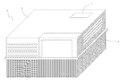
図1は、実施の形態1における電力変換装置の外観を表す斜視図、図2は、実施の形態1における電力変換装置の分解斜視図、図3は、実施の形態1における要部縦断面図、図4は、実施の形態1の展開例を表した要部斜視図である。図1と図2に示すように、電力変換装置1は、底面が開放された絶縁性部材等の樹脂材料からなる本体ケース2と、本体ケース2の底面を覆うように設けられた冷却フィン5とを有する。
FIG. 1 is a perspective view showing an external appearance of the power conversion device according to the first embodiment, FIG. 2 is an exploded perspective view of the power conversion device according to the first embodiment, and FIG. FIG. 4 is a perspective view of a main part showing a development example of the first embodiment. As shown in FIGS. 1 and 2, the power conversion device 1 includes a
本体ケース2は、上面に操作パネル部3が設けられ、側面に通風を可能とする通風口2aや外部配線を行うための窓部2bが形成される。操作パネル部3は、後述する主回路基板20と図示しないケーブルによって接続されており、操作パネル部3で入力した運転指令がこのケーブルを介して主回路基板20に伝えられる。冷却フィン5は、矩形状の金属板からなり本体ケース2の底面となるベース部5bと、ベース部5bの下面に所定間隔を空けて一体に並設された一群の金属板からなる羽根部5aとからなる。そして、羽根部5aの一方の端部に対向して冷却ファン6が配置される。
The
図2と図3に示すように、冷却フィン5のベース部5bのほぼ中央部には矩形状の開口部5bxが形成され、さらに羽根部5aにはベース部5bの開口部5bxと対向する位置に所定深さの切り欠き部5axが形成されており、開口部5bxと切り欠き部5axが一体となって空間部5cを形成する。空間部5cは、冷却ファン6に対向する位置に配置することが好ましい。なお、この空間部5cは矩形状に限定されない。
As shown in FIGS. 2 and 3, a rectangular opening 5bx is formed at a substantially central portion of the base portion 5b of the
一方、ノイズフィルタ回路を実装するノイズフィルタ回路基板7には、ノイズフィルタ回路を構成するフィルタ素子のうち発熱する発熱部品であるフィルタ素子11が一方の面に実装され、ノイズフィルタ回路を主回路基板20に接続する一群の接続端子12が他方の面に実装されている。
On the other hand, on the noise
なお、図2に示した接続端子12は矩形の端子となっているが、矩形以外の形状の端子を使用してもよく、また、被覆電線をノイズフィルタ回路基板7にハンダ付けして、この被覆電線を介してノイズフィルタ回路基板7と主回路基板20とを接続するようにしてもよい。また、その他の電気的に接続できる特性を有する導体で所定の絶縁距離が確保できるような接続方法を使用してもよい。
The
そして、ノイズフィルタ回路基板7は、ベース部5bの開口部5bxを塞ぐようにベース部5bに重ねられ、四隅をねじ8により固定される。このとき、ノイズフィルタ回路基板7はフィルタ素子11の実装された面を下向きにされるとともに、フィルタ素子11は空間部5cの内部に収納され、また、フィルタ素子11の通電部が羽根部5aおよびベース部5bの導電部と所定の絶縁距離を保つようにした状態で固定される。なお、ノイズフィルタ回路基板7は、ねじ以外の方法でベース部5bに固定してもよい。
The noise
一方、冷却フィン5のベース部5bの上面には、冷却ファン6に近接対向する位置にIGBT等の主回路素子から成り電力変換回路の一部である主回路モジュール9が配置され、冷却フィン5を介して放熱できるようにねじ10によってベース部5bに密着固定される。一般には主回路モジュール9と冷却フィン5の密着度および熱伝導性を向上させるために、主回路モジュール9と冷却フィン5の間に専用のゲルが注入される。
On the other hand, on the upper surface of the base portion 5 b of the cooling
さらに、ベース部5bには、ベース部5bと略同形状であり、主回路モジュール9とともに電力変換等を行う主回路基板20が取付けられる。詳しくは、主回路基板20はベース部5bの四隅に立設された所定高さの固定具14にねじ21で締付けられることによって固定される。この固定具14によって、ベース部5bと主回路基板20との間にノイズフィルタ回路基板7及び主回路モジュール9を収納する所定高さの空間が保持される。
Further, a
ベース部5bと主回路基板20との固定には、前記固定具14を用いる方法の他に、ベース部5bの四隅に円柱状の突起構造をベース部5bと一体化して設け、この突起構造にねじ穴を施しておき、ベース部5bと主回路基板20とをねじで締付固定するようにしてもよい。なお、主回路基板20は複数枚の基盤で構成されていてもよく、これらの基板が垂直方向あるいは水平方向に並べて配置された構造であってもよい。
For fixing the base portion 5b and the
また、主回路基板20には、ノイズフィルタ回路基板7及び主回路モジュール9の上面に設けられた各接続端子12、13にそれぞれ対向位置して接続される接続端子22、23が設けられる。
In addition, the
そして、主回路基板20の上面には、電力変換回路の一部である主回路コンデンサ24と、電力変換装置1を図示しない外部電源やモータに接続するための入出力端子台25と、図示しない電力変換などを行う回路とがそれぞれ実装される。このとき、入出力端子台25は本体ケース2の窓部2bに臨ませて配置される。なお、入出力端子台25は、入力端子台と出力端子台を分けて、それぞれ主回路基板上に実装するようにしてもよく、さらに、入力端子台と出力端子台は近接配置されていなくてもよい。
On the upper surface of the
次に、実施の形態1における電力変換装置の動作を説明する。図3に示すように、冷却ファン6が駆動されると、冷却風が冷却フィン5の羽根部5aの間を点線矢印の向きに流れ、主回路モジュール9で発生する熱を羽根部5aを介して放熱する。この冷却風は、同時にフィルタ素子11に直接当たり、フィルタ素子11を冷却する。
Next, the operation of the power conversion device according to Embodiment 1 will be described. As shown in FIG. 3, when the cooling fan 6 is driven, the cooling air flows between the
例えば、フィルタ素子11がリアクトルである場合、発熱の要因は主に巻線の銅損である。この銅損は巻線の直径や通電電流値などによって変化し、巻線の直径が細くなるほど、通電電流値が大きくなるほど銅損は多くなる。一方で、巻線の直径が細くできればリアクトルにおける巻線間の絶縁距離の確保が容易となり、またリアクトルのコアサイズも小さくすることが可能となる。
For example, when the
潤工社の電線ハンドブック112ページに示された許容電流グラフを参考にすると、直径0.8mmと0.5mmの絶縁電線(絶縁体厚は0.3mm)において、1気圧の下で10Aの電流を通電した場合の導体上昇温度は、前者が約45deg、後者が約100degとなる。このように導体の直径を0.8mmから0.5mmに若干細くするだけで導体上昇温度が2倍程度に大きくなることが判る。一方で、前記の2種類の径の絶縁電線を使用してコアに20ターンすることを考えた場合、巻線に必要なスペースとして絶縁電線が占める面積を算出すると、直径0.8mmの導体を使用した場合は約19mm2、直径0.5mmの導体を使用した場合は約10mm2となり、2倍程度も異なることが分かる。前記の面積差はリアクトルの寸法に直接に影響する。 Referring to the allowable current graph shown on page 112 of Junko's Electric Wire Handbook, when 10A of current is applied under 1 atm on an insulated wire with a diameter of 0.8mm and 0.5mm (insulator thickness is 0.3mm) The conductor rising temperature is about 45 deg for the former and about 100 deg for the latter. Thus, it can be seen that the conductor rising temperature can be increased by a factor of about 2 only by reducing the diameter of the conductor slightly from 0.8 mm to 0.5 mm. On the other hand, when considering the above-mentioned two types of insulated wires with 20 diameters to the core and calculating the area occupied by the insulated wires as the space required for the winding, a conductor with a diameter of 0.8 mm is used. It is about 19mm 2 , and about 10mm 2 when a conductor with a diameter of 0.5mm is used. The area difference directly affects the dimensions of the reactor.
よって、リアクトルの発熱を外部から冷却することが出来れば、巻線径が細くても巻き線の温度上昇を低減することができるため、結果としてリアクトルを小型化することが可能となる。 Therefore, if the heat generation of the reactor can be cooled from the outside, the temperature rise of the winding can be reduced even if the winding diameter is small, and as a result, the reactor can be downsized.
また、海外規格のUL60950で規定された最小沿面距離を参考にすると、汚損度合2の場合は、動作電圧200Vにおいて約1mm〜2mm、動作電圧400Vにおいて約2mm〜4mmの沿面距離を確保する必要がある。前期のように巻線径を細くすることができれば、単相または三相のリアクトルにおいて、巻線に必要となるスペースを小さくでき、結果として、相間の沿面距離を確保しやすくなる。
Also, referring to the minimum creepage distance specified by UL60950 of the overseas standard, in the case of
なお、図3に示す空間部5cに元々設けてあった羽根部5aがなくなることによる主回路モジュール9の冷却性能低下が許容されない場合、本実施例ではフィルタ素子11により冷却風の流れのほとんどを遮るような構造でないため、羽根部5aの枚数を増やすか、もしくは、冷却フィン5を熱伝導性に優れる材料で作製することなどの対策を講じることにより冷却性能を改善することが可能である。
In the present embodiment, when the reduction in the cooling performance of the main circuit module 9 due to the absence of the
また、外部から空間部5cに入り込んだ異物がフィルタ素子11または空間部5cに接するノイズフィルタ回路基板7に異物が接触することを避けたい場合、異物の接触を避けたい部分を覆うようにカバーやゲル等を施してもよい。この場合、熱伝導性と電気絶縁性を有する材料を採用することが望ましい。
Further, when it is desired to prevent foreign matter that has entered the space 5c from the outside from coming into contact with the
さらに、主回路コンデンサ24の主回路基板への取り付け位置は、図2に限定されない。図4に示すように、冷却フィン5のベース部5bより大きな外形を有する主回路基板30を用いて、主回路基板30と冷却フィン5の側面部とで囲まれる空間に配置して主回路基板30に取り付けるようにしてもよい。
Furthermore, the attachment position of the
実施の形態1の電力変換装置によれば、ノイズフィルタ回路を内蔵する電力変換装置において、冷却フィンに空間部を形成し、この空間部にノイズフィルタ回路を構成するフィルタ素子を収納させてノイズフィルタ回路基板をベース部に固定することにより、フィルタ素子を効率的に冷却することができるとともに、電力変換装置全体の小型化が可能となる。また、ノイズフィルタ回路基板を冷却フィン上に設けた開口部に収納してベース部に固定する構造としたことで、振動の発生頻度が多い環境下においてもノイズフィルタ回路基板の脱落回避を低コストで実現することができる。 According to the power conversion device of the first embodiment, in the power conversion device incorporating the noise filter circuit, a space portion is formed in the cooling fin, and the filter element constituting the noise filter circuit is accommodated in the space portion, thereby the noise filter. By fixing the circuit board to the base portion, the filter element can be efficiently cooled, and the entire power conversion device can be downsized. In addition, the noise filter circuit board is housed in an opening provided on the cooling fin and fixed to the base part, so that the noise filter circuit board can be prevented from falling off even in an environment where vibrations are frequently generated. Can be realized.
本実施例においては冷却ファンを使用した構成を示したが、冷却ファンを使用せずに自然空冷による放熱を行っている電力変換装置であっても本実施例のようにノイズフィルタ回路基板を設置することで同様の効果を得ることができる。 In this embodiment, a configuration using a cooling fan is shown. However, a noise filter circuit board is installed as in this embodiment even in a power converter that dissipates heat by natural air cooling without using a cooling fan. By doing so, the same effect can be obtained.
なお、ノイズフィルタ回路基板7とベース部5bが接する箇所のベース部5bに、ノイズフィルタ回路基板7の厚み寸法と同等の深さの窪みを設けておいてもよい。このような窪みを設けることによって、ノイズフィルタ回路基板7をベース部5bに固定した構造と合わせて、振動が起きやすい環境下でもノイズフィルタ回路基板7が脱落しにくくなる。また、前記窪みは製品量産時においてノイズフィルタ回路基板7をベース部5bに配置し易くするという効果も有する。
A recess having a depth equivalent to the thickness dimension of the noise
実施の形態2.
本発明に係る実施の形態2を、図5〜6を参照して説明する。
A second embodiment according to the present invention will be described with reference to FIGS.
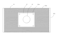
図5は、実施の形態2におけるノイズフィルタ回路基板40の上面図であり、異なる2つの例(a)、(b)を示している。図6は、実施の形態2における電力変換装置の要部縦断面図である。ここで、実施の形態1と同一又は同等の部分は、同じ符号を用いるものとし、その詳細の説明を省略する。ノイズフィルタ回路基板40は、実施の形態1と同様に、冷却フィン5のベース部5bの開口部5bxを塞ぐように、ねじ8によってベース部5bに固定される。そして、ノイズフィルタ回路基板40の下面に実装されたフィルタ素子42は、冷却フィン5に形成された空間部5c内を冷却ファン6側に偏って配置されている。したがって、空間部5cの吸い込み側に所定幅の隙間が形成される。
FIG. 5 is a top view of the noise filter circuit board 40 according to the second embodiment, and shows two different examples (a) and (b). FIG. 6 is a longitudinal sectional view of a main part of the power conversion device according to the second embodiment. Here, parts that are the same as or equivalent to those in Embodiment 1 are denoted by the same reference numerals, and detailed description thereof is omitted. Similarly to the first embodiment, the noise filter circuit board 40 is fixed to the base portion 5b by the screw 8 so as to close the opening 5bx of the base portion 5b of the cooling
ノイズフィルタ回路基板40には、空間部5cの隙間に対向位置して、スリット43が貫通して形成される。スリット43の例としては、図5の(a)図に示すように空間部5cの幅ほどの長さを有するスリット43xや、図5の(b)図に示すように空間部5cの上方にて並設される一群のスリット43yなどがある。 In the noise filter circuit board 40, a slit 43 is formed so as to penetrate the gap of the space 5c. As an example of the slit 43, as shown in FIG. 5A, a slit 43x having a length about the width of the space portion 5c, or above the space portion 5c as shown in FIG. 5B. And a group of slits 43y arranged side by side.
そして、スリット43と冷却ファン6との間でノイズフィルタ回路基板40の上面には、別のフィルタ素子41等の発熱部品が実装される。フィルタ素子41は、スリット43に対向して配置されることが好ましい。 A heat generating component such as another filter element 41 is mounted on the upper surface of the noise filter circuit board 40 between the slit 43 and the cooling fan 6. The filter element 41 is preferably arranged to face the slit 43.
なお、外部から空間部5cに入り込んだ異物がスリット43を介してノイズフィルタ回路基板40の上面の回路等に接触することを避けたい場合、異物の接触を避けたい部分を覆うようにカバーやゲル等を施しても良い。この場合、電気絶縁性を有する材料を採用することが望ましい。 In addition, when it is desired to prevent foreign matter that has entered the space 5c from the outside from coming into contact with the circuit on the upper surface of the noise filter circuit board 40 through the slit 43, a cover or gel is provided so as to cover the portion from which foreign matter contact is to be avoided. Etc. may be applied. In this case, it is desirable to employ a material having electrical insulation.
次に、実施の形態2における電力変換装置の動作を説明する。図6に示すように、冷却ファン6が駆動されると、冷却風が冷却フィン5の羽根部5aの間を点線矢印の向きに流れ、主回路モジュール9で発生する熱を羽根部5aを介して放熱する。この冷却風は、同時に羽根部5aの内側に形成された空間部5c内に位置したフィルタ素子42に直接当たり、フィルタ素子42を冷却する。また、この冷却風の一部はスリット43を通ってノイズフィルタ回路基板40の上面へと流れ、ノイズフィルタ回路基板40のの上面に実装したフィルタ素子41等の発熱部品に当たってこれを冷却し、本体ケース2の通風口2aから外部へ流出する。
Next, the operation of the power conversion device according to
実施の形態2の電力変換装置によれば、実施の形態1の効果に加えて、ノイズフィルタ回路基板の上面に実装された発熱部品を同時に冷却することができる。 According to the power conversion device of the second embodiment, in addition to the effects of the first embodiment, the heat generating component mounted on the upper surface of the noise filter circuit board can be simultaneously cooled.
実施の形態3.
本発明に係る実施の形態3を、図2と図4を参照して説明する。
A third embodiment according to the present invention will be described with reference to FIGS.
図2に示すように、ノイズフィルタ回路基板7は冷却フィン5のベース部5bの上面のほぼ中央部に配置され、ノイズフィルタ回路基板7と近接対向して主回路モジュール9がベース部5bの上面に配置される。そして、主回路基板20の上面には、ノイズフィルタ回路基板7を挟んで主回路モジュール9と反対側に入出力端子台25が配置される。
As shown in FIG. 2, the noise
ここで、入出力端子台25は、本体ケース2の窓部2bを通して電力変換装置1の外部電源やモータなどと接続される。そして、ノイズフィルタ回路基板7は、主回路モジュール9の動作に起因して発生する伝導ノイズを低減する。このように伝導ノイズを低減することで、入出力端子台25を介して外部電源に伝導ノイズが伝達するのを抑制する。
Here, the input /
また、図2の展開例である図4では、ノイズフィルタ回路基板7と主回路モジュール9とが図2と同様に配置される。一方、ノイズフィルタ回路基板7の主回路モジュール9と反対側には、入出力端子台32が冷却フィン5のベース部5bの上面に配置される。すなわち、主回路モジュール9と入出力端子台32との間に、ノイズフィルタ回路基板7が配置される。
Further, in FIG. 4, which is a development example of FIG. 2, the noise
実施の形態3の電力変換装置によれば、空間的及び電気的に入出力端子台と主回路モジュールとの間にノイズフィルタ回路基板が介在する配置を取るため、入出力端子台とノイズフィルタ回路基板と主回路モジュールとをほぼ一直線上に配置でき、入出力端子台とノイズフィルタ回路基板との間、及びノイズフィルタ回路基板と主回路モジュールとの間の配線を最短接続することが容易となる。このような最短接続は配線のインダクタンスや、配線間および配線と周囲導体との間に存在する浮遊容量を低減することができるために共振要因低減および浮遊容量を介したノイズ伝播経路の削減に効果があり、結果として伝導ノイズの低減効果を向上させることが可能となる。 According to the power conversion device of the third embodiment, since the noise filter circuit board is disposed between the input / output terminal block and the main circuit module spatially and electrically, the input / output terminal block and the noise filter circuit are arranged. The board and the main circuit module can be arranged almost in a straight line, and it is easy to make the shortest connection between the input / output terminal block and the noise filter circuit board and between the noise filter circuit board and the main circuit module. . Such shortest connection can reduce the inductance of wiring and stray capacitance existing between wirings and between wiring and surrounding conductors, so it is effective in reducing resonance factor and noise propagation path through stray capacitance. As a result, it is possible to improve the effect of reducing conduction noise.
実施の形態4.
本発明に係る実施の形態4を、図7〜8を参照して説明する。
Embodiment 4 FIG.
Embodiment 4 according to the present invention will be described with reference to FIGS.
図7は、実施の形態4におけるノイズフィルタ回路基板7の下面図、図8は、実施の形態4における電力変換装置の要部縦断面図である。ここで、実施の形態1と同一又は同等の部分は、同じ符号を用いるものとし、その詳細の説明を省略する。本実施の形態では、図8に示すように、ノイズフィルタ回路基板7の下面と冷却フィン5のベース部5bの上面との接触領域において、導電性部材からなる導電部70を配置する。導電部70はノイズフィルタ回路基板7において接地が必要な箇所に設ける。この導電部70は例えば、ノイズフィルタ回路基板7の下面周縁部に所定幅で予め形成された導電パターンなどである。
FIG. 7 is a bottom view of the noise
そして、ノイズフィルタ回路基板7を冷却フィン5のベース部5bの上面に重ねてその四隅を導電性部材からなるねじ73によって冷却フィン5のベース部5bに固定する。これによって、導電部70が冷却フィン5のベース部5bと電気的に接続される。
Then, the noise
一方、冷却フィン5のベース部5bには、接地(以下、GND)線72を接続するGND端子71が設けられており、導電部70はGNDと同電位となる。ここで、GND端子71は、ベース部5bの上面のうち、図4の入出力端子台32の近傍に配置することが望ましい。あるいは、図2、図4の入出力端子台25、32に直接固定することも可能である。
On the other hand, the base portion 5b of the cooling
また、導電部70とベース部5bとが接するベース部5bの側の面を研磨して極力凹凸を無くし、導電部70とベース部5bの密着度を高めるようにしてもよい。さらに前記密着度を高めるために、矩形状の絶縁部材からなり、その両端部にネジ穴を有する固定具を用意し、この固定具でノイズフィルタ回路基板7の周囲をベース部5bに押さえつけるように固定してもよい。
Further, the surface on the side of the base portion 5b where the
実施の形態1では、ノイズフィルタ回路基板を接地する必要がある場合はノイズフィルタ回路基板上にGND端子を設けておき、冷却フィンのベース部又は入出力端子台に固定されたGND端子から、ノイズフィルタ回路基板のGND端子に配線しなければならないが、実施の形態4によれば、GND端子からノイズフィルタ回路基板の導電部までの配線が不要となり、ノイズフィルタ回路基板の導電部を最短で接地することが可能である。また、導電部とベース部とが接する面積を広くすることができるため、配線を使用した接続方法に比べて、導電部とベース部間に存在するインピーダンスを低減することが可能となる。 In the first embodiment, when it is necessary to ground the noise filter circuit board, a ground terminal is provided on the noise filter circuit board, and noise is generated from the ground terminal fixed to the base portion of the cooling fin or the input / output terminal block. Although wiring to the GND terminal of the filter circuit board is required, according to the fourth embodiment, wiring from the GND terminal to the conductive part of the noise filter circuit board is not required, and the conductive part of the noise filter circuit board is grounded in the shortest time. Is possible. In addition, since the area where the conductive portion and the base portion are in contact with each other can be increased, impedance existing between the conductive portion and the base portion can be reduced as compared with a connection method using wiring.
例えば、ノイズフィルタ回路基板で接地する必要がある場合とは、Yコンデンサを実装している場合などである。一般に、Yコンデンサは電源線の各相とGND線との間に接続され、コモンモードの伝導ノイズ低減に効果がある。コモンモードの伝導ノイズは電力変換装置→出力電源線の各相→負荷装置(モータ等)→出力GND線→電力変換装置→入力GND線→外部電源→入力電源線の各相→電力変換装置のような還流経路で伝播する。入力電源線の各相と入力GND線との間にYコンデンサを設置すれば、入力電源線の各相と入力GND線との間のインピーダンスを低くすることができるため、コモンモードの伝導ノイズがYコンデンサに流れ込みやすくなり、結果として、コモンモードの伝導ノイズが入力GND線を介して外部電源に流出するのを抑制することができる。よって、Yコンデンサをノイズフィルタ回路基板に実装する際には、Yコンデンサと入力電源線の各相、およびYコンデンサとGND線との間のインピーダンスを極力低減した方がよい。このため導電部とベース部間に存在するインピーダンスを低減すれば、結果として伝導ノイズの低減効果を向上させることが可能となる。 For example, the case where the noise filter circuit board needs to be grounded is the case where a Y capacitor is mounted. In general, the Y capacitor is connected between each phase of the power supply line and the GND line, and is effective in reducing common mode conduction noise. Common mode conduction noise is: power converter → each phase of output power line → load device (motor, etc.) → output GND line → power converter → input GND line → external power supply → each phase of input power line → power converter Propagated in such a reflux path. If a Y capacitor is installed between each phase of the input power supply line and the input GND line, the impedance between each phase of the input power supply line and the input GND line can be lowered. As a result, the common mode conduction noise can be prevented from flowing out to the external power supply via the input GND line. Therefore, when the Y capacitor is mounted on the noise filter circuit board, it is preferable to reduce the impedance between the Y capacitor and the input power supply line and between the Y capacitor and the GND line as much as possible. For this reason, if the impedance existing between the conductive portion and the base portion is reduced, the effect of reducing conductive noise can be improved as a result.
実施の形態5.
本発明に係る実施の形態5を、図9〜11を参照して説明する。
図9は、実施の形態5における冷却フィン90の下面図、図10は、実施の形態5における冷却フィンの縦断面図、図11は、実施の形態5における付属冷却フィンの下面図および縦断面図である。ここで、実施の形態1と同一又は同等の部分は、同じ符号を用いるものとし、その詳細の説明を省略する。この実施の形態5では、図10に示すように、冷却フィン90の羽根部90aのほぼ中央部に、羽根部90aを切り欠いて形成された高さ方向を貫通する矩形状の開口部90axが形成される。 9 is a bottom view of the cooling fin 90 in the fifth embodiment, FIG. 10 is a longitudinal sectional view of the cooling fin in the fifth embodiment, and FIG. 11 is a bottom view and longitudinal section of the accessory cooling fin in the fifth embodiment. FIG. Here, parts that are the same as or equivalent to those in Embodiment 1 are denoted by the same reference numerals, and detailed description thereof is omitted. In the fifth embodiment, as shown in FIG. 10, a rectangular opening 90ax penetrating in the height direction formed by cutting out the blade portion 90a is formed at a substantially central portion of the blade portion 90a of the cooling fin 90. It is formed.
ノイズフィルタ回路基板91は、下面にフィルタ素子92が実装され、羽根部90aの開口部90ax側からその内部に収納され、ベース部90bの下面に固定される。そして、ノイズフィルタ回路基板91と、ベース部90bの上面に設置された図2に示す主回路モジュール9や主回路基板20などとの間の電気的接続は、ベース部90bの中央部に予め形成した開口部90bxを通して行われる。また、ノイズフィルタ回路基板91の上面には、ベース部90bの開口部90bxの内部に収納される、図示しない別のフィルタ素子を実装することが可能である。
The filter element 92 is mounted on the lower surface of the noise filter circuit board 91, and is housed therein from the opening 90ax side of the blade 90a, and is fixed to the lower surface of the base 90b. The electrical connection between the noise filter circuit board 91 and the main circuit module 9 and the
さらに、羽根部90aの開口部90axの内部には、図11に示すような付属冷却フィン110が取り外し自在に収納され、ノイズフィルタ回路基板91の下面に接着固定される。ここで、付属冷却フィン110は、羽根部90aの開口部90axとほぼ同じ大きさの付属ベース部110dと、この付属ベース部110dの一方の面に設けられた付属羽根部110bと、付属ベース部110dの他方の面の両端部に設けられた一対のL字形保持片110aとからなる。 Further, an accessory cooling fin 110 as shown in FIG. 11 is removably accommodated in the opening 90ax of the blade portion 90a, and is adhered and fixed to the lower surface of the noise filter circuit board 91. Here, the attached cooling fin 110 includes an attached base portion 110d having the same size as the opening 90ax of the blade portion 90a, an attached blade portion 110b provided on one surface of the attached base portion 110d, and an attached base portion. It consists of a pair of L-shaped holding pieces 110a provided at both ends of the other surface of 110d.
付属冷却フィン110は、L字形保持片110aの端部とノイズフィルタ回路基板91の四隅とに金属性部材からなるねじ111を下方から挿通することにより、冷却フィン90のベース部90bの下面に固定される。この固定状態で、冷却フィン110の付属ベース部110dとフィルタ素子92とが接触しないように、L字形保持片110aの高さが決められる。 The attached cooling fin 110 is fixed to the lower surface of the base portion 90b of the cooling fin 90 by inserting screws 111 made of a metal member from below into the end of the L-shaped holding piece 110a and the four corners of the noise filter circuit board 91. Is done. In this fixed state, the height of the L-shaped holding piece 110a is determined so that the attached base portion 110d of the cooling fin 110 and the filter element 92 do not contact each other.
次に、実施の形態5における電力変換装置の動作を説明する。主回路モジュール9で発生する熱は、冷却フィン90のベース部90b→羽根部90aの経路、及び冷却フィン90のベース部90b→ねじ111→付属冷却フィン110の一対のL字形保持片110a→付属羽根部110bの経路で伝播する。そして、図10に示すように、冷却ファン6が駆動されると、冷却風が冷却フィン90の羽根部90aの間、付属冷却フィン110の一対のL字形保持片110aの間、及び付属羽根部110bの間を点線矢印の向きに流れる。
Next, the operation of the power conversion device according to
このうち、冷却フィン90の羽根部90aの間、及び付属冷却フィン110の付属羽根部110bの間を流れる冷却風は、主回路モジュール9で発生する熱を放熱する。同時に、一対のL字形保持片110aの間を流れる冷却風は、フィルタ素子92に直接当たり、フィルタ素子92を冷却する。 Among these, the cooling air flowing between the blade portions 90 a of the cooling fin 90 and between the auxiliary blade portions 110 b of the attached cooling fin 110 radiates heat generated in the main circuit module 9. At the same time, the cooling air flowing between the pair of L-shaped holding pieces 110 a directly hits the filter element 92 and cools the filter element 92.
実施の形態1では、ノイズフィルタ回路基板は接続端子を介して主回路基板及び主回路モジュールと一体化して固定されている。したがってノイズフィルタ回路基板を冷却フィンのベース部から取り外す際には、主回路基板及び主回路モジュールと共に取り外す必要がある。しかし、主回路モジュールの冷却面が冷却フィンに専用ゲルやはんだによって密着固定されている場合、ノイズフィルタ回路基板の冷却フィンのベース部からの取り外し及び再取り付けには、はんだ処理や専用ゲル塗布などの作業が発生し労力がかかることとなる。 In the first embodiment, the noise filter circuit board is integrally fixed to the main circuit board and the main circuit module via the connection terminals. Therefore, when removing the noise filter circuit board from the base portion of the cooling fin, it is necessary to remove it together with the main circuit board and the main circuit module. However, if the cooling surface of the main circuit module is closely fixed to the cooling fin with a dedicated gel or solder, the removal or reattachment of the noise filter circuit board from the base of the cooling fin may be performed by soldering or special gel application. This will cause a lot of work.
実施の形態5の電力変換装置によれば、付属冷却フィンとノイズフィルタ回路基板の取り外し及び再取り付けを容易に行うことが可能である。これによって、フィルタ素子を構成するフェライトコア等の部材を容易に交換することができる。また、取り外し可能な付属冷却フィンによって冷却フィンの冷却能力を補完するため、実施の形態1とほぼ同等な冷却能力を得ることができる。 According to the power conversion device of the fifth embodiment, it is possible to easily remove and reattach the attached cooling fin and the noise filter circuit board. Thereby, members such as a ferrite core constituting the filter element can be easily replaced. In addition, since the cooling capacity of the cooling fins is supplemented by the removable cooling fins that can be removed, it is possible to obtain a cooling capacity substantially equivalent to that of the first embodiment.
実施の形態6.
本発明に係る実施の形態6を、図12〜13を参照して説明する。
Embodiment 6 FIG.
A sixth embodiment according to the present invention will be described with reference to FIGS.
図12は、実施の形態6における冷却フィン120の下面図、図13は、実施の形態6における付属冷却フィンの下面図および縦断面図である。ここで、実施の形態5と同一又は同等の部分は、同じ符号を用いるものとし、その詳細の説明を省略する。この実施の形態6では、図12に示すように、冷却フィン120の羽根部120aのほぼ中央部を高さ方向に貫通するとともに、冷却風の流れと直交する方向に貫通して切り欠くことにより、開口部120axが形成される。 FIG. 12 is a bottom view of the cooling fin 120 in the sixth embodiment, and FIG. 13 is a bottom view and a longitudinal sectional view of the accessory cooling fin in the sixth embodiment. Here, the same reference numerals are used for the same or equivalent parts as in the fifth embodiment, and the detailed description thereof is omitted. In the sixth embodiment, as shown in FIG. 12, the substantially central portion of the blade portion 120a of the cooling fin 120 penetrates in the height direction and is cut out in a direction perpendicular to the flow of the cooling air. The opening 120ax is formed.
実施の形態5と同様に、ノイズフィルタ回路基板91は、下面に実装されたフィルタ素子92と共に羽根部120aの開口部120axの内部に収納され、ベース部120bの開口部を塞ぐようにベース部120bの下面に固定される。そして、ノイズフィルタ回路基板91の四隅を、ねじ111によってベース部120bの下面に固定される。ノイズフィルタ回路基板91と主回路基板20に実装した主回路モジュール9とは、実施の形態5と同じように開口部120axに対向してベース部120bに形成した図示しない開口部を通して電気的に接続される。
As in the fifth embodiment, the noise filter circuit board 91 is housed inside the opening 120ax of the blade 120a together with the filter element 92 mounted on the lower surface, and the base 120b is closed so as to close the opening of the base 120b. It is fixed to the lower surface. Then, the four corners of the noise filter circuit board 91 are fixed to the lower surface of the base portion 120b by screws 111. As in the fifth embodiment, the noise filter circuit board 91 and the main circuit module 9 mounted on the
さらに、羽根部120aの開口部120axの内部には、図13に示すような付属の冷却フィン130が取り外し可能に収納され、ベース部120bの下面に固定される。付属冷却フィン130は、羽根部120aの開口部120axとほぼ同じ大きさの付属ベース部130dと、付属ベース部130dの一方の面に設けられた付属羽根部130bと、付属ベース部130dの他方の面の両端部に設けられた一対のL字形保持片130aとからなる。このL字形保持片130aは、実施の形態5と同様に、付属冷却フィン130の付属羽根部130aとフィルタ素子92とが接触しないような高さであり、その端部を、金属性部材からなるねじ131によってベース部120bの下面に固定される。 Further, an accessory cooling fin 130 as shown in FIG. 13 is detachably accommodated in the opening 120ax of the blade 120a, and is fixed to the lower surface of the base 120b. The accessory cooling fin 130 includes an accessory base portion 130d having substantially the same size as the opening 120ax of the blade portion 120a, an accessory blade portion 130b provided on one surface of the accessory base portion 130d, and the other of the accessory base portion 130d. It consists of a pair of L-shaped holding pieces 130a provided at both ends of the surface. As in the fifth embodiment, the L-shaped holding piece 130a has such a height that the attached vane portion 130a of the attached cooling fin 130 and the filter element 92 do not come into contact with each other, and its end portion is made of a metallic member. The screw 131 is fixed to the lower surface of the base part 120b.
実施の形態6における電力変換装置の動作は、実施の形態5と同様である。 The operation of the power conversion device in the sixth embodiment is the same as that in the fifth embodiment.
実施の形態5では、ノイズフィルタ回路基板を収納する冷却フィンの羽根部の開口部が、羽根部を冷却風の流れと直交する方向に貫通しないため、全長の異なる3種類の金属板によって羽根部を構成させる必要があった。一方、実施の形態6の電力変換装置によれば、全長の異なる2種類の金属板によって構成させるに足りるため、実施の形態5と比して冷却フィンの製作を容易にすることが可能である。また、取り外し可能な付属冷却フィンは、冷却フィンの冷却能力を補完するため、実施の形態1とほぼ同等な冷却能力を得ることができる。
In
実施の形態7.
本発明に係る実施の形態7を、図14を参照して説明する。
A seventh embodiment according to the present invention will be described with reference to FIG.
図14は、実施の形態7における電力変換装置の要部斜視図である。ここで、実施の形態1と同一又は同等の部分は、同じ符号を用いるものとし、その詳細の説明を省略する。 FIG. 14 is a perspective view of a main part of the power conversion device according to the seventh embodiment. Here, parts that are the same as or equivalent to those in Embodiment 1 are denoted by the same reference numerals, and detailed description thereof is omitted.
実施の形態1と同様に、ノイズフィルタ回路基板7はねじ8によって冷却フィン5のベース部5bに取り付けられる。そして、冷却フィン5のベース部5bには、主回路基板140が設置される。詳しくは、主回路基板140は、ベース部5bの上面に立設された固定具14にねじ21が締付けられることによって固定される。
As in the first embodiment, the noise
主回路基板140には、ノイズフィルタ回路基板7の上方において、ノイズフィルタ回路基板7より大きな外形を有する開口部140aが形成される。そして、ノイズフィルタ回路基板7と主回路基板140との間の電気的接続は、主回路基板140の開口部140aを通して行われる。
In the
実施の形態1では、ノイズフィルタ回路基板は接続端子を介して主回路基板及び主回路モジュールと一体化して固定されている。したがってノイズフィルタ回路基板を冷却フィンのベース部から取り外す際には、主回路基板及び主回路モジュールと共に取り外す必要がある。しかし、主回路モジュールの冷却面が冷却フィンに専用ゲルやはんだによって密着固定されているため、ノイズフィルタ回路基板の冷却フィンのベース部からの取り外し及び再取り付けには、はんだ処理や専用ゲル塗布などの作業が発生し労力がかかることとなる。 In the first embodiment, the noise filter circuit board is integrally fixed to the main circuit board and the main circuit module via the connection terminals. Therefore, when removing the noise filter circuit board from the base portion of the cooling fin, it is necessary to remove it together with the main circuit board and the main circuit module. However, because the cooling surface of the main circuit module is tightly fixed to the cooling fins with a special gel or solder, the removal and reattachment of the noise filter circuit board from the base of the cooling fins requires soldering or special gel application. This will cause a lot of work.
実施の形態7の電力変換装置によれば、主回路基板等を取り外すことなく、ノイズフィルタ回路基板の取り外し及び取り付けを主回路基板の開口部を通して容易に行うことが可能である。これによって、フィルタ素子を構成するフェライトコア等の部材を容易に交換することが可能である。 According to the power conversion device of the seventh embodiment, it is possible to easily remove and attach the noise filter circuit board through the opening of the main circuit board without removing the main circuit board or the like. Thereby, it is possible to easily replace a member such as a ferrite core constituting the filter element.
実施の形態8.
本発明に係る実施の形態8を、図15を参照して説明する。
Embodiment 8 FIG.
An eighth embodiment according to the present invention will be described with reference to FIG.
図15は、実施の形態8における電力変換装置の要部分解斜視図である。ここで、実施の形態1及び実施の形態7と同一又は同等の部分は、同じ符号を用いるものとし、その詳細の説明を省略する。
FIG. 15 is an exploded perspective view of main parts of the power conversion device according to the eighth embodiment. Here, parts that are the same as or equivalent to those in
実施の形態7の主回路基板140に形成された開口部140aは、開口部140aより大きな外形を有する取り外し可能な付属基板151によって塞がれる。詳しくは、主回路基板140の上面には、開口部140a近傍にコネクタ150が固定される。一方、付属基板151の下面には、コネクタ150に対向する位置にコネクタ152が設けられる。そして、付属基板151は、コネクタ152とコネクタ150とが接続することによって、主回路基板140に電気的に接続される。
The opening 140a formed in the
実施の形態8の電力変換装置によれば、実施の形態7の効果に加えて、取り外し可能な付属基板によって、主回路基板全体の面積を補完あるいは増大することができる。 According to the power conversion device of the eighth embodiment, in addition to the effects of the seventh embodiment, the area of the entire main circuit board can be supplemented or increased by the removable accessory board.
9 主回路モジュール
11、41、42、92 フィルタ素子
5、90、120 冷却フィン
5a、90b、120b ベース部
5b、90a、120a 羽根部
5bx、90ax、120ax 開口部
5ax 切り欠き部
5c、90bx 空間部
7、40、91 ノイズフィルタ回路基板
43 スリット
25、32 入出力端子台
70 導電部
71 GND端子
72 GND線
20、30、140 主回路基板
151 付属基板
110、130 付属冷却フィン
110a、130a L字形保持片
110b、130b 付属羽根部
110d、130d 付属ベース部
140a 基板側開口部
9
Claims (11)
ベース部と羽根部を有し、前記ベース部に前記主回路モジュールを取り付けた冷却フィンと、
外部電源と前記電力変換回路との間に接続されるノイズフィルタ回路が実装されたノイズフィルタ回路基板とを備える電力変換装置において、
前記冷却フィンは、前記ベース部に開口部が形成されるとともに、前記羽根部に前記開口部と一体となって空間部を形成する切り欠き部が形成され、
前記ノイズフィルタ回路基板は、前記ノイズフィルタ回路を構成する発熱部品を前記空間部の内部に収納するとともに、前記開口部を塞ぐように前記ベース部に固定されることを特徴とする電力変換装置。 A main circuit module on which a power conversion circuit is mounted;
A cooling fin having a base portion and a blade portion, and the main circuit module being attached to the base portion;
In a power converter comprising a noise filter circuit board on which a noise filter circuit connected between an external power source and the power converter circuit is mounted.
In the cooling fin, an opening is formed in the base portion, and a notch portion is formed in the blade portion to form a space portion integrally with the opening portion,
The said noise filter circuit board is fixed to the said base part so that the heat-emitting components which comprise the said noise filter circuit may be accommodated in the inside of the said space part, and the said opening part may be plugged up.
ベース部と羽根部を有し、前記ベース部に前記主回路モジュールを取り付けた冷却フィンと、
外部電源と前記電力変換回路との間に接続されるノイズフィルタ回路が実装されたノイズフィルタ回路基板とを備える電力変換装置において、
前記冷却フィンは、前記羽根部に高さ方向を貫通する開口部が形成され、
前記ノイズフィルタ回路基板は、前記ノイズフィルタ回路を構成する発熱部品とともに前記開口部の内部に収納されるとともに、前記ベース部に固定されることを特徴とする電力変換装置。 A main circuit module on which a power conversion circuit is mounted;
A cooling fin having a base portion and a blade portion, and the main circuit module being attached to the base portion;
In a power converter comprising a noise filter circuit board on which a noise filter circuit connected between an external power source and the power converter circuit is mounted.
The cooling fin is formed with an opening penetrating in the height direction in the blade portion,
The noise filter circuit board is housed in the opening together with the heat generating components constituting the noise filter circuit, and is fixed to the base portion.
前記付属冷却フィンは、前記開口部に収納され、前記ノイズフィルタ回路部品を前記付属ベース部と前記L字形保持片とによって囲まれた空間の内部に収納した状態で前記ベース部に固定されることを特徴とする請求項9または10記載の電力変換装置。 Attached base portion having substantially the same size as the opening, an attached vane portion provided on one surface of the attached base portion, and a pair of L-shapes provided at both ends of the other surface of the attached base portion An accessory cooling fin having a holding piece,
The accessory cooling fin is housed in the opening, and is fixed to the base in a state where the noise filter circuit component is housed in a space surrounded by the accessory base and the L-shaped holding piece. The power converter according to claim 9 or 10.
Priority Applications (1)
| Application Number | Priority Date | Filing Date | Title |
|---|---|---|---|
| JP2008273238A JP2010104146A (en) | 2008-10-23 | 2008-10-23 | Power converting apparatus |
Applications Claiming Priority (1)
| Application Number | Priority Date | Filing Date | Title |
|---|---|---|---|
| JP2008273238A JP2010104146A (en) | 2008-10-23 | 2008-10-23 | Power converting apparatus |
Publications (1)
| Publication Number | Publication Date |
|---|---|
| JP2010104146A true JP2010104146A (en) | 2010-05-06 |
Family
ID=42294251
Family Applications (1)
| Application Number | Title | Priority Date | Filing Date |
|---|---|---|---|
| JP2008273238A Withdrawn JP2010104146A (en) | 2008-10-23 | 2008-10-23 | Power converting apparatus |
Country Status (1)
| Country | Link |
|---|---|
| JP (1) | JP2010104146A (en) |
Cited By (6)
| Publication number | Priority date | Publication date | Assignee | Title |
|---|---|---|---|---|
| JP2012228021A (en) * | 2011-04-18 | 2012-11-15 | Yaskawa Electric Corp | Electric power conversion apparatus and filter switch |
| CN104066805A (en) * | 2012-01-23 | 2014-09-24 | 旭化成电子材料株式会社 | Coating composition and antireflection film |
| JP2016119375A (en) * | 2014-12-19 | 2016-06-30 | ホシデン株式会社 | Photoelectric conversion module and active optical cable |
| JP2017153347A (en) * | 2016-02-24 | 2017-08-31 | エルエス産電株式会社Lsis Co., Ltd. | Motor drive unit |
| JP2019012652A (en) * | 2017-06-30 | 2019-01-24 | 株式会社豊田自動織機 | Battery module and battery pack |
| CN111699157A (en) * | 2017-12-11 | 2020-09-22 | 日产化学株式会社 | Inorganic oxide particles coated with silane compound containing nitrogen ring, and coating composition |
-
2008
- 2008-10-23 JP JP2008273238A patent/JP2010104146A/en not_active Withdrawn
Cited By (9)
| Publication number | Priority date | Publication date | Assignee | Title |
|---|---|---|---|---|
| JP2012228021A (en) * | 2011-04-18 | 2012-11-15 | Yaskawa Electric Corp | Electric power conversion apparatus and filter switch |
| CN104066805A (en) * | 2012-01-23 | 2014-09-24 | 旭化成电子材料株式会社 | Coating composition and antireflection film |
| CN104066805B (en) * | 2012-01-23 | 2017-05-03 | 旭化成株式会社 | Coating composition and antireflection film |
| JP2016119375A (en) * | 2014-12-19 | 2016-06-30 | ホシデン株式会社 | Photoelectric conversion module and active optical cable |
| JP2017153347A (en) * | 2016-02-24 | 2017-08-31 | エルエス産電株式会社Lsis Co., Ltd. | Motor drive unit |
| US9936600B2 (en) | 2016-02-24 | 2018-04-03 | Lsis Co., Ltd. | Motor drive unit |
| JP2019012652A (en) * | 2017-06-30 | 2019-01-24 | 株式会社豊田自動織機 | Battery module and battery pack |
| JP7027708B2 (en) | 2017-06-30 | 2022-03-02 | 株式会社豊田自動織機 | Battery module and battery pack |
| CN111699157A (en) * | 2017-12-11 | 2020-09-22 | 日产化学株式会社 | Inorganic oxide particles coated with silane compound containing nitrogen ring, and coating composition |
Similar Documents
| Publication | Publication Date | Title |
|---|---|---|
| CN102916566A (en) | Power supply unit using housing in which printed circuit board is housed | |
| JP2010104146A (en) | Power converting apparatus | |
| JPH1051912A (en) | Electric apparatus having heat radiating fin | |
| JP2018198304A (en) | Coil device, substrate-equipped coil device, and electrical junction box | |
| CN113330679A (en) | Power conversion device | |
| WO2021220563A1 (en) | Power conversion device | |
| JP4389573B2 (en) | Power supply | |
| EP0432670A2 (en) | Converter and discharge-lamp operating apparatus using the converter | |
| JP2011258852A (en) | Semiconductor device | |
| JP2019169638A (en) | Heating component mounting structure | |
| JP2020047765A (en) | Electrical device and radiator | |
| JP2007259539A (en) | Vehicle-mounted electrical connection box | |
| JP3876770B2 (en) | Wiring structure | |
| JP5717922B1 (en) | Power converter | |
| JP2012227424A (en) | Semiconductor device | |
| JP7192918B1 (en) | Busbar heat dissipation structure and inverter device | |
| CN220510989U (en) | Electric control device, inversion control equipment and energy storage power supply | |
| JP4169907B2 (en) | Electronic control unit | |
| JP5454438B2 (en) | Semiconductor module | |
| JP7395329B2 (en) | power converter | |
| JPH0992992A (en) | Electric machine | |
| JP2017028057A (en) | Electronic circuit device | |
| JP2006310557A (en) | Switching unit | |
| JP6607053B2 (en) | Power supply | |
| US8142205B2 (en) | Electronic apparatus |
Legal Events
| Date | Code | Title | Description |
|---|---|---|---|
| A621 | Written request for application examination |
Free format text: JAPANESE INTERMEDIATE CODE: A621 Effective date: 20110224 |
|
| A761 | Written withdrawal of application |
Free format text: JAPANESE INTERMEDIATE CODE: A761 Effective date: 20121116 |