JP2010103805A - Bending vibration piece, bending vibrator, and piezoelectric device - Google Patents
Bending vibration piece, bending vibrator, and piezoelectric device Download PDFInfo
- Publication number
- JP2010103805A JP2010103805A JP2008273987A JP2008273987A JP2010103805A JP 2010103805 A JP2010103805 A JP 2010103805A JP 2008273987 A JP2008273987 A JP 2008273987A JP 2008273987 A JP2008273987 A JP 2008273987A JP 2010103805 A JP2010103805 A JP 2010103805A
- Authority
- JP
- Japan
- Prior art keywords
- bending vibration
- bending
- hole
- vibration piece
- piece
- Prior art date
- Legal status (The legal status is an assumption and is not a legal conclusion. Google has not performed a legal analysis and makes no representation as to the accuracy of the status listed.)
- Withdrawn
Links
Images


Landscapes
- Oscillators With Electromechanical Resonators (AREA)
- Piezo-Electric Or Mechanical Vibrators, Or Delay Or Filter Circuits (AREA)
Abstract
Description
本発明は、屈曲振動片、屈曲振動子、および圧電デバイスに関する。 The present invention relates to a bending vibration piece, a bending vibrator, and a piezoelectric device.
従来から、屈曲振動片を小型化するとQ値が小さくなり、屈曲振動を阻害することが知られている。これは、熱の移動により温度平衡させるまでの緩和時間に反比例する緩和振動と、屈曲振動片の振動周波数とが、近づいて起こる熱弾性効果によるものである。つまり、屈曲振動片が屈曲振動することにより弾性変形が生じ、圧縮される面の温度は上昇し、伸張される面の温度は下降するため、屈曲振動片の内部に温度差が発生する。この温度差を熱伝導により温度平衡させるまでの緩和時間に反比例する緩和振動により、屈曲振動を阻害し、Q値を低下させる。
このため、屈曲振動片の屈曲振動部に溝または貫通孔を形成し、振動子の圧縮される面から伸張される面に発生する熱の移動を阻止して、熱弾性効果に起因するQ値変動の抑制を図っている(たとえば、特許文献1参照)。
Conventionally, it is known that when a flexural vibration piece is miniaturized, the Q value becomes small and the flexural vibration is inhibited. This is due to the thermoelastic effect that occurs when the relaxation vibration that is inversely proportional to the relaxation time until the temperature is balanced by the movement of heat and the vibration frequency of the flexural vibration piece approach each other. That is, elastic deformation is caused by bending vibration of the bending vibration piece, the temperature of the surface to be compressed is increased, and the temperature of the surface to be expanded is decreased, so that a temperature difference is generated inside the bending vibration piece. Bending vibration is inhibited and the Q value is lowered by relaxation vibration that is inversely proportional to the relaxation time until the temperature difference is balanced by heat conduction.
For this reason, a groove or a through-hole is formed in the bending vibration portion of the bending vibration piece to prevent the movement of heat generated on the surface that is expanded from the surface to be compressed of the vibrator, and the Q value resulting from the thermoelastic effect Fluctuation is suppressed (see, for example, Patent Document 1).
しかしながら、上述の従来技術を用いても、熱弾性効果に起因するQ値劣化は十分に改善されない。本願発明者らは、屈曲振動により生じた熱の一部が、屈曲振動部に設けた溝または貫通孔を迂回して移動してしまうという現象の存在を新たに見出すと共に、熱の移動は屈曲振動部に設けた溝または貫通孔の基部側(自由端側ではなく基部側)で特に顕著になることも新たに見出した。即ち、上述の従来技術においては、屈曲振動片の固定される一端側にまでは、貫通溝または貫通孔が形成されていないため一端側において熱の移動が発生するため、屈曲振動によって屈曲振動片の伸張される面と圧縮される面との間で、熱の移動を阻止できない。このため、熱弾性効果に起因するQ値の変動を抑制することは困難という課題がある。 However, even if the above-described conventional technique is used, the Q value deterioration due to the thermoelastic effect is not sufficiently improved. The inventors of the present application newly found the existence of a phenomenon in which a part of heat generated by bending vibration moves around a groove or a through hole provided in the bending vibration portion, and the movement of heat is bent. It has also been newly found that it becomes particularly prominent on the base side (the base side, not the free end side) of the groove or the through-hole provided in the vibration part. That is, in the above-described prior art, since the through groove or the through hole is not formed up to the one end side where the bending vibration piece is fixed, heat transfer occurs at one end side. Heat transfer cannot be prevented between the stretched surface and the compressed surface. For this reason, there exists a subject that it is difficult to suppress the fluctuation | variation of Q value resulting from a thermoelastic effect.
本発明は、熱弾性効果に起因するQ値劣化が、屈曲振動を行う屈曲振動部だけでなく、屈曲振動部に接続された基部においても生じるという新たな発見に基づくものであり、上記課題の少なくとも一部を解決するためになされたものである。以下の形態または適用例により実現することが可能である。 The present invention is based on a new discovery that the Q value deterioration caused by the thermoelastic effect occurs not only in the bending vibration part that performs bending vibration but also in the base part connected to the bending vibration part. It was made to solve at least a part. It can be realized by the following forms or application examples.
[適用例1]本適用例にかかる屈曲振動片は、基部と、前記基部から延長して形成され、屈曲振動する屈曲振動部とを備え、前記屈曲振動部は、それぞれ対向して配置され屈曲振動により互い違いに伸張するおよび圧縮する第1面および第2面と、前記第1面と前記第2面との間を貫通する貫通孔とを備え、前記貫通孔は、前記屈曲振動部から前記基部に跨って形成されていることを要旨とする。 [Application Example 1] A bending vibration piece according to this application example includes a base and a bending vibration part that is formed extending from the base and bends and vibrates. The bending vibration parts are arranged to be opposed to each other and bend. A first surface and a second surface that alternately expand and compress by vibration, and a through-hole penetrating between the first surface and the second surface, the through-hole from the bending vibration portion The gist is that it is formed across the base.
これによれば、屈曲振動により互い違いに伸張するおよび圧縮する第1面および第2面の間に、貫通孔を形成し、貫通孔は屈曲振動部から基部に跨って形成されているので、第1面と第2面との間での熱移動経路を確保することができず、貫通孔により遮ることができる。このようにして、第1面と第2面との間での熱移動経路を、屈曲振動部だけでなく基部においても貫通孔により遮断するので、熱移動(熱伝導)により温度平衡させるまでの緩衝時間に反比例する緩和振動を無くし、屈曲振動数を阻害することを抑制することができる。これにより、熱弾性効果に起因するQ値の変動を抑制し、屈曲振動片の小型化を実現することができる。 According to this, since the through hole is formed between the first surface and the second surface that are alternately expanded and compressed by the bending vibration, and the through hole is formed from the bending vibration portion to the base portion, A heat transfer path between the first surface and the second surface cannot be secured and can be blocked by the through hole. In this way, the heat transfer path between the first surface and the second surface is blocked not only by the bending vibration part but also by the through-hole at the base part, so that the temperature balance is achieved by heat transfer (heat conduction). It is possible to eliminate relaxation vibration that is inversely proportional to the buffer time, and to inhibit the bending frequency from being inhibited. Thereby, the fluctuation | variation of Q value resulting from a thermoelastic effect can be suppressed, and size reduction of a bending vibration piece can be implement | achieved.
[適用例2]上記適用例にかかる屈曲振動片において、前記貫通孔の端部のうち、前記屈曲振動部に設けられた全ての端部が、前記屈曲振動部の延長方向の長さの半分の位置から前記基部側に配置されていることが好ましい。 Application Example 2 In the bending vibration piece according to the application example described above, of the end portions of the through hole, all the end portions provided in the bending vibration portion are half the length in the extension direction of the bending vibration portion. It is preferable that it is arrange | positioned from the position of the said base side.
これによれば、屈曲振動による熱の移動の比較的多い部分である基部から屈曲振動部の延長方向の長さの半分の位置から前記基部側にかけて、貫通孔が配置されているので、上述の効果を奏することができる。そして、屈曲振動による熱の移動の比較的少ない部分である屈曲振動部の延長方向の長さの半分を超えた部分(自由端側)の機械的強度を確保することができる。 According to this, since the through-hole is arranged from the base portion, which is a relatively large portion of heat transfer due to bending vibration, to the base portion side from the half of the length in the extending direction of the bending vibration portion, the above-mentioned There is an effect. And the mechanical strength of the part (free end side) exceeding half the length of the extension direction of the bending vibration part which is a part with comparatively little heat transfer by bending vibration is securable.
[適用例3]本適用例にかかる屈曲振動子は、上記記載の前記屈曲振動片と、前記屈曲振動片とを収納するパッケージとを備え、前記パッケージ内に前記屈曲振動片が気密に封止されたことを要旨とする。 Application Example 3 A bending vibrator according to this application example includes the bending vibration piece described above and a package that houses the bending vibration piece, and the bending vibration piece is hermetically sealed in the package. It is a summary.
これによれば、屈曲振動子は、上述と同様の効果を奏することができる。 According to this, the bending vibrator can exhibit the same effect as described above.
[適用例4]本適用例にかかる圧電デバイスは、上記記載の前記屈曲振動片と、前記屈曲振動子を駆動させるICチップと、前記屈曲振動片および前記ICチップを収納するパッケージとを備え、前記パッケージ内に前記屈曲振動片および前記ICチップが気密に封止されたことを要旨とする。 Application Example 4 A piezoelectric device according to this application example includes the bending vibration piece described above, an IC chip that drives the bending vibrator, and a package that houses the bending vibration piece and the IC chip. The gist is that the flexural vibration piece and the IC chip are hermetically sealed in the package.
これによれば、圧電デバイスは、上述と同様の効果を奏することができる。 According to this, the piezoelectric device can exhibit the same effects as described above.
以下の実施形態では、屈曲振動片として圧電体の一種である水晶からなる水晶振動片を一例に挙げて説明する。そして、この水晶振動片を用いた圧電振動子および圧電デバイスとして、水晶振動子および水晶発振器を例に挙げて説明する。 In the following embodiments, a quartz crystal vibrating piece made of quartz, which is a kind of piezoelectric body, will be described as an example of the bending vibrating piece. Then, as a piezoelectric vibrator and a piezoelectric device using the crystal vibrating piece, a crystal vibrator and a crystal oscillator will be described as examples.
(第1実施形態)
以下、第1実施形態について、図1および図2を参照して説明する。
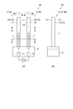
図1は、第1実施形態の水晶振動片10を示す概略図である。図2は、図1の概略断面図である。
(First embodiment)
The first embodiment will be described below with reference to FIGS. 1 and 2.
FIG. 1 is a schematic diagram illustrating a quartz
図1(a)は、水晶振動片10の正面概略図である。図1(b)は、図1(a)の側面概略図である。
図1に示すように、水晶振動片10は、屈曲振動部1と、基部2と、貫通孔7と、固定電極5,6を備えている。
FIG. 1A is a schematic front view of the quartz
As shown in FIG. 1, the quartz
屈曲振動部1は、基部2から延長して形成されている。屈曲振動部1は、それぞれ対向して配置された第1面11および第2面12、ならびにそれぞれ対向して配置された第3面13および第4面14を備えている。
The
貫通孔7は、第3面13と第4面14との間を貫通して形成されている。そして、貫通孔7は、第1面11と第2面12との間に、配置されている。また、貫通孔7は、屈曲振動部1から基部2に跨って形成されている。そして、貫通孔7は、基部2から屈曲振動部1が延長する方向の長さの半分の位置から基部2側まで、形成されている。
The through
固定電極5,6は、基部2に配置されている。固定電極5,6の間には、交流電流が流れるように配線されている。
The
屈曲振動部1、基部2、および貫通孔7は、水晶の原石から切り出した後、ウェットエッチングなどにより、形成される。固定電極5,6は、クロム(Cr)またはニッケル(Ni)などの下地層と、この下地層の上に金(Au)または銀(Ag)などからなる電極層とを備えている。これら下地層および電極層は、蒸着またはスパッタリングなどにより形成される。
The
屈曲振動部1が実線矢印および2点鎖線矢印で示す面外振動にて屈曲振動するに伴い、第1面11および第2面12には、互い違いに圧縮および伸張が生じる。なお、面外振動とは、屈曲振動部1の延長方向および屈曲振動部1の幅方向のいずれにも略垂直である変位を伴う振動のことをいう。
第1面11に圧縮が生じるとき、第2面12に伸張が生じる。そして逆に、第1面11に伸張が生じるとき、第2面12に圧縮が生じる。このようにして、それぞれ対向して配置された第1面11および第2面12は、屈曲振動部1の屈曲振動により互い違いに伸張する、および圧縮する。
As the
When the
図2(a)は、図1(b)のA−A概略断面図である。図2(b)は、図1(b)のB−B概略断面図である。
図2(a)に示すように、屈曲振動部1の第1面11および第2面12に、励振電極3が形成されている。そして、屈曲振動部1の第3面13および第4面14に、励振電極4が形成されている。
図2(b)に示すように、貫通孔7に、励振電極4が形成されている。励振電極3は、図2(a)と同様に、第1面11および第2面12に形成されている。
このようにして、励振電極3,4の間には、交流電流が流れるように配線されている。
Fig.2 (a) is AA schematic sectional drawing of FIG.1 (b). FIG. 2B is a schematic cross-sectional view taken along the line BB in FIG.
As shown in FIG. 2A, the
As shown in FIG. 2B, the
In this way, the
励振電極3,4は、クロム(Cr)またはニッケル(Ni)などの下地層と、この下地層の上に金(Au)または銀(Ag)などからなる電極層とを備えている。これら下地層および電極層は、蒸着またはスパッタリングなどにより形成される。
The
励振電極3は固定電極5に接続され、励振電極4は固定電極6に接続されている(図示省略)。固定電極5,6の間に交流電流を流すことにより、励振電極3,4の間に交流電流が流れる。これにより、励振電極3,4により挟まれた屈曲振動部1に電界が発生する。そして、励振電極3,4に、正電荷および負電荷が互い違いに帯電するため、電界の方向が変化する。この電界の発生方向に応じて、第1面11および第2面12に、圧電効果による伸張および圧縮が生じる。このようにして、屈曲振動部1は、図1(b)に実線矢印および2点鎖線矢印で示す屈曲振動をする。
The
また、固定電極5および固定電極6は、水晶振動片10を収納するパッケージ(図示省略)などに固定するためにも用いられる。
Further, the fixed
したがって、本実施形態によれば、屈曲振動により互い違いに伸張するおよび圧縮する第1面11および第2面12の間に、貫通孔7を形成し、貫通孔7は屈曲振動部1から基部2に跨って形成されているので、第1面11と第2面12との間での熱移動経路を確保することができず、貫通孔7により遮ることができる。このようにして、第1面11と第2面12との間での熱移動経路を、屈曲振動部1だけでなく基部2においても貫通孔7により遮断するので、熱移動(熱伝導)により温度平衡させるまでの緩衝時間に反比例する緩和振動を無くし、屈曲振動数を阻害することを抑制することができる。これにより、熱弾性効果に起因するQ値の変動を抑制し、水晶振動片10の小型化を実現することができる。
Therefore, according to the present embodiment, the through
これによれば、屈曲振動による熱の移動の比較的多い部分である基部2から屈曲振動部1の延長方向の長さの半分の位置から基部2側にかけて、貫通孔7が配置されているので、上述の効果を奏することができる。そして、屈曲振動による熱の移動の比較的少ない部分である屈曲振動部1の延長方向の長さの半分を超えた部分(自由端側)の機械的強度を確保することができる。
According to this, since the through-
(第2実施形態)
以下、第2実施形態について、図3および図4を参照して説明する。
図3は、第2実施形態の水晶振動片20を示す概略図である。図4は、図3の概略断面図である。
(Second Embodiment)
Hereinafter, the second embodiment will be described with reference to FIGS. 3 and 4.
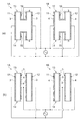
FIG. 3 is a schematic view showing the
第2実施形態の水晶振動片20は、図1および図2に示した第1実施形態の屈曲振動部1を2個備えたことが相違する点である。このため、同一の符号を付与し、構成の説明を省略する。
The
図3(a)は、水晶振動片20の正面概略図である。図3(b)は、図3(a)の側面概略図である。
図3に示すように、水晶振動片20は、2個の屈曲振動部1(1A,1B)と、基部2と、2個の貫通孔7と、固定電極5,6を備えている。
FIG. 3A is a schematic front view of the
As shown in FIG. 3, the quartz
2個の屈曲振動部1(1A,1B)は、基部2からそれぞれ延長して形成されている。2個の屈曲振動部1には、それぞれ貫通孔7が形成されている。
The two bending vibration parts 1 (1A, 1B) are formed extending from the
屈曲振動部1(1A,1B)が実線矢印および2点鎖線矢印で示す面外振動にて屈曲振動するに伴い、第1面11および第2面12には、互い違いに圧縮および伸張が生じる。なお、面外振動とは、第1実施形態でも説明したとおり、屈曲振動部1の延長方向および屈曲振動部1の幅方向のいずれにも略垂直である変位を伴う振動のことである。特に本実施形態の場合は、面外振動を、屈曲振動部1(1A,1B)の延長方向および屈曲振動部1(1A,1B)の配列方向のいずれにも略垂直である変位を伴う振動と説明することもできる。
第1面11に圧縮が生じるとき、第2面12に伸張が生じる。そして逆に、第1面11に伸張が生じるとき、第2面12に圧縮が生じる。このようにして、それぞれ対向して配置された第1面11および第2面12は、屈曲振動部1(1A,1B)の屈曲振動により互い違いに伸張する、および圧縮する。
As the bending vibration part 1 (1A, 1B) bends and vibrates due to out-of-plane vibration indicated by a solid arrow and a two-dot chain line arrow, the
When the
図4(a)は、図3(b)のA−A概略断面図である。図4(b)は、図3(b)のB−B概略断面図である。
図4(a)に示すように、屈曲振動部1Aには、励振電極3,4が図2(a)と同様に形成されている。それに対して、屈曲振動部1Bには、励振電極3,4が図2(a)とは相違して形成されている。つまり、屈曲振動部1Bの第1面11および第2面12に、励振電極4が形成され、第3面13および第4面14に、励振電極3が形成されている。
図4(b)に示すように、屈曲振動部1Aには、図2(b)と同様に、第1面11および第2面12に、励振電極3が形成されている。それに対して、屈曲振動部1Bには、励振電極3,4が図2(b)とは相違して形成されている。つまり、屈曲振動部1Bの第1面11および第2面12に、励振電極4が形成されている。そして、屈曲振動部1Bの貫通孔7に、励振電極3が形成されている。
このようにして、励振電極3,4の間には、交流電流が流れるように配線されている。
Fig.4 (a) is AA schematic sectional drawing of FIG.3 (b). FIG. 4B is a schematic cross-sectional view taken along the line BB in FIG.
As shown in FIG. 4A,
As shown in FIG. 4B, the
In this way, the
このように、励振電極3,4の間に交流電流を流すことにより、屈曲振動部1Aが実線矢印で示す屈曲振動するとき、屈曲振動部1Bは2点鎖線矢印で示す屈曲振動する。そして逆に、屈曲振動部1Aが2点鎖線矢印で示す屈曲振動するとき、屈曲振動部1Bは実線矢印で示す屈曲振動する。
As described above, when the bending
したがって、本実施形態によれば、上述の実施形態と同様の効果を奏することができる。 Therefore, according to this embodiment, the same effect as the above-mentioned embodiment can be produced.
(第3実施形態)
以下、第3実施形態について、図5および図6を参照して説明する。
図5は、第3実施形態の水晶振動片30を示す概略図である。図6は、図5の概略断面図である。
(Third embodiment)
Hereinafter, the third embodiment will be described with reference to FIGS. 5 and 6.
FIG. 5 is a schematic view showing a
第3実施形態の水晶振動片30、図3および図4に示した第2実施形態の水晶振動片20と相違する点は、屈曲振動部1(1A,1B)の屈曲振動方向である。このため、同一の符号を付与し、構成の説明を省略する。
The difference between the
図5(a)は、水晶振動片30の正面概略図である。図5(b)は、図5(a)の側面概略図である。
図5に示すように、水晶振動片30は、2個の屈曲振動部1(1A,1B)と、基部2と、2個の貫通孔7と、固定電極5,6を備えている。
FIG. 5A is a schematic front view of the
As shown in FIG. 5, the quartz
図5に示す水晶振動片30は、図3に示した2個の屈曲振動部1(1A,1B)、および2個の貫通孔7をそれぞれ、屈曲振動部の延長方向を軸に90°回転させた配置である。
The
屈曲振動部1(1A,1B)が実線矢印および2点鎖線矢印で示す面内振動にて屈曲振動するに伴い、第1面11および第2面12には、互い違いに圧縮および伸張が生じる。
第1面11に圧縮が生じるとき、第2面12に伸張が生じる。そして逆に、第1面11に伸張が生じるとき、第2面12に圧縮が生じる。このようにして、それぞれ対向して配置された第1面11および第2面12は、屈曲振動部1(1A,1B)の屈曲振動により互い違いに伸張する、および圧縮する。
As the bending vibration part 1 (1A, 1B) bends and vibrates due to the in-plane vibration indicated by the solid arrow and the two-dot chain arrow, the
When the
図6(a)は、図5(a)のA−A概略断面図である。図6(b)は、図5(a)のB−B概略断面図である。
図6(a)および図6(b)に示すように、屈曲振動部1A,1Bには、励振電極3,4が図4(a)および図4(b)と同様に形成されている。
このようにして、励振電極3,4の間には、交流電流が流れるように配線されている。
Fig.6 (a) is AA schematic sectional drawing of Fig.5 (a). FIG.6 (b) is BB schematic sectional drawing of Fig.5 (a).
As shown in FIGS. 6A and 6B,
In this way, the
このように、励振電極3,4の間に交流電流を流すことにより、屈曲振動部1Aが実線矢印で示す屈曲振動するとき、屈曲振動部1Bは同じく実線矢印で示す屈曲振動する。そして逆に、屈曲振動部1Aが2点鎖線矢印で示す屈曲振動するとき、屈曲振動部1Bは同じく2点鎖線矢印で示す屈曲振動する。
In this way, when an alternating current is passed between the
したがって、本実施形態によれば、上述の実施形態と同様の効果を奏することができる。 Therefore, according to this embodiment, the same effect as the above-mentioned embodiment can be produced.
(第4実施形態)
以下、第4実施形態について、図7および図8を参照して説明する。
図7は、第4実施形態の水晶振動片40を示す概略図である。図8は、図7の概略断面図である。
(Fourth embodiment)
Hereinafter, the fourth embodiment will be described with reference to FIGS. 7 and 8.
FIG. 7 is a schematic view showing a
第4実施形態の水晶振動片40、図5および図6に示した第3実施形態の水晶振動片30と相違する点は、屈曲振動部1(1A,1B)にそれぞれスリット部16を備えた点である。このため、同一の符号を付与し、構成の説明を省略する。
The difference between the
図7(a)は、水晶振動片40の正面概略図である。図7(b)は、図7(a)の側面概略図である。
図7に示すように、水晶振動片40は、2個の屈曲振動部1(1A,1B)と、基部2と、2個の貫通孔7と、4個のスリット部16と、固定電極5,6を備えている。
FIG. 7A is a schematic front view of the
As shown in FIG. 7, the quartz
図7に示す水晶振動片40は、屈曲振動部1(1A,1B)の第3面13および第4面14に、それぞれスリット部16を備えている。
A
屈曲振動部1(1A,1B)が実線矢印および2点鎖線矢印で示す面内振動にて屈曲振動するに伴い、第1面11および第2面12には、互い違いに圧縮および伸張が生じる。
第1面11に圧縮が生じるとき、第2面12に伸張が生じる。そして逆に、第1面11に伸張が生じるとき、第2面12に圧縮が生じる。このようにして、それぞれ対向して配置された第1面11および第2面12は、屈曲振動部1(1A,1B)の屈曲振動により互い違いに伸張する、および圧縮する。
As the bending vibration part 1 (1A, 1B) bends and vibrates due to the in-plane vibration indicated by the solid arrow and the two-dot chain arrow, the
When the
図8(a)は、図7(a)のA−A概略断面図である。図8(b)は、図7(a)のB−B概略断面図である。
図8(a)に示すように、屈曲振動部1Aのスリット部16には、励振電極4が形成されている。屈曲振動部1Bのスリット部16には、励振電極3が形成されている。
図8(b)に示すように、屈曲振動部1A,1Bには、励振電極3,4が図6(b)と同様に形成されている。
このようにして、励振電極3,4の間には、交流電流が流れるように配線されている。
Fig.8 (a) is AA schematic sectional drawing of Fig.7 (a). FIG. 8B is a schematic cross-sectional view taken along the line BB in FIG.
As shown in FIG. 8A, the
As shown in FIG. 8B,
In this way, the
このように、励振電極3,4の間に交流電流を流すことにより、屈曲振動部1Aが実線矢印で示す屈曲振動するとき、屈曲振動部1Bは同じく実線矢印で示す屈曲振動する。そして逆に、屈曲振動部1Aが2点鎖線矢印で示す屈曲振動するとき、屈曲振動部1Bは同じく2点鎖線矢印で示す屈曲振動する。
In this way, when an alternating current is passed between the
したがって、本実施形態によれば、上述の実施形態と同様の効果を奏することができる。 Therefore, according to this embodiment, the same effect as the above-mentioned embodiment can be produced.
(第5実施形態)
以下、第5実施形態の圧電振動子として水晶振動子を一例に挙げ、図9および図10を参照して説明する。
(Fifth embodiment)
Hereinafter, a crystal resonator will be described as an example of the piezoelectric resonator of the fifth embodiment, and a description will be given with reference to FIGS. 9 and 10.
第5実施形態の水晶振動子は、第1から第4実施形態の水晶振動片を用いた水晶振動子である。このため、第5実施形態の水晶振動子に用いる水晶振動片は、第1から第4実施形態の水晶振動片と同様の構成であるため、同一の符号を付与し、構成の説明を省略する。以下では、第3実施形態の水晶振動片30を用いて説明する。
The crystal resonator of the fifth embodiment is a crystal resonator using the crystal resonator element of the first to fourth embodiments. For this reason, the quartz crystal resonator element used for the quartz crystal resonator of the fifth embodiment has the same configuration as the quartz crystal resonator element of the first to fourth embodiments, so that the same reference numerals are given and description of the configuration is omitted. . Below, it demonstrates using the
図9は、蓋体を除いて内部構造を露出した水晶振動子の概略平面図である。図10は、図9のX−X概略断面図であり、蓋体を配置して示すものである。
図9および図10に示すように、水晶振動子80は、パッケージ31内に水晶振動片30を収納している。具体的には、水晶振動子80は、図10に示すように、第1基板34と、この第1基板34に積層された第2基板35と第3基板36とを含むパッケージ31内に水晶振動片30を収納している。
FIG. 9 is a schematic plan view of the crystal unit with the internal structure exposed except for the lid. FIG. 10 is a schematic cross-sectional view taken along the line XX in FIG. 9 and shows a lid disposed.
As shown in FIGS. 9 and 10, the
パッケージ31は、絶縁基体である第1基板34と第2基板35と第3基板36とを構成している。第2基板35がパッケージ31内に延長した延長部35aを備えている。延長部35aに電極部32が2個形成されている。電極部32に、導電ペーストなどを用いて水晶振動片30の固定電極5および固定電極6を、固定して、導通させる。ここで、導電性接着剤43としては、所定の合成樹脂でなるバインダ成分に、銀粒子などの導電粒子を添加したものを使用することができる。
The
第1基板34と第2基板35と第3基板36とは絶縁材料で形成され、セラミックが適している。特に、好ましい材料としては水晶振動片30や蓋体37の熱膨張係数と一致もしくは、きわめて近い熱膨張係数を備えたものが選択され、本実施形態では、例えば、セラミックのグリーンシートが利用されている。グリーンシートは、例えば、所定の溶液中にセラミックパウダを分散させ、バインダを添加して生成される混練物をシート状の長いテープ形状に成形し、これを所定の長さにカットして得られるものである。
The
第1基板34と第2基板35と第3基板36とは、図示する形状に成形したグリーンシートを積層し、焼結して形成することができる。この場合、第1基板34は、パッケージ31の底部を構成する基板で、これに重ねられる第2基板35と第3基板36とは、上述したグリーンシートを板状として、内部の材料を除去して、枠状として、図10の内部空間Sを形成したもので、この内部空間Sを利用して、水晶振動片30を収納するようにしている。このパッケージ31には、セラミックやガラスあるいはコバールなどの金属で形成された蓋体37がコバールリングなどの接合材もしくは封止材47などを介して接合されている。これにより、パッケージ31は気密に封止されている。
The
第1基板34上には、例えば、銀・パラジウムなどの導電ペーストもしくはタングステンメタライズなどの導電ペーストなどを用いて、必要とされる導電パターンを形成後に、第1基板34と第2基板35と第3基板36との焼結をした後で、ニッケルおよび金もしくは銀などを順次メッキして、上述した電極部32が形成されている。
図10に示すように、電極部32は、パッケージ31の底面に露出した少なくとも2個の実装端子41と図示しない導電パターンにより接続されている。この電極部32と実装端子41とを接続するための導電パターンは、パッケージ31の形成時に利用されるキャスタレーション(図示せず)の表面に形成して、パッケージ31の外面を引き回してもよいし、あるいは第1基板34と第2基板35とを貫通する導電スルーホールなどにより接続してもよい。
On the
As shown in FIG. 10, the
2個の実装端子41の間に交流電圧を印加することにより、固定電極5と固定電極6との間に、交流電流が流れる(図4参照)。これにより、水晶振動片30は、上述の実施形態で実線矢印および2点鎖線矢印で示した屈曲振動をする。
By applying an AC voltage between the two mounting
したがって、第5実施形態によれば、上述の実施形態と同様の効果を奏する水晶振動子を得ることができる。 Therefore, according to the fifth embodiment, it is possible to obtain a crystal resonator that exhibits the same effect as the above-described embodiment.
(第6実施形態)
以下、第6実施形態の圧電デバイスとして水晶発振器を一例に挙げて説明する。
(Sixth embodiment)
Hereinafter, a crystal oscillator will be described as an example of the piezoelectric device of the sixth embodiment.
第6実施形態の水晶発振器は、第1から第4実施形態の水晶振動片を用いた水晶発振器である。このため、第6実施形態の水晶発振器に用いる水晶振動片は、第1から第4実施形態の水晶振動片と同様の構成であるため、同一の符号を付与し、構成の説明を省略する。以下では、第3実施形態の水晶振動片30を用いて説明する。また、第5実施形態と第6実施形態の相違する点は、第6実施形態の水晶発振器は、第5実施形態で示した水晶振動子に、水晶振動子を駆動させる駆動回路を含むICチップを備えた点である。
The crystal oscillator of the sixth embodiment is a crystal oscillator using the crystal resonator element of the first to fourth embodiments. For this reason, since the crystal vibrating piece used for the crystal oscillator of the sixth embodiment has the same configuration as the crystal vibrating piece of the first to fourth embodiments, the same reference numerals are given and description of the configuration is omitted. Below, it demonstrates using the
図11に示すように、パッケージ31を形成する第1基板34上面には、金(Au)などから成る内部接続端子89が形成されている。ICチップ87は、パッケージ31を形成する第1基板34上面に接着剤などを用いて固定されている。そして、ICチップ87の上面には、Auなどから成るIC接続パッド82が形成されている。IC接続パッド82は、金属ワイヤー88により内部接続端子89に接続されている。また、内部接続端子89は内部配線を経由して、パッケージ31外部の第1基板34下面に形成された実装端子41に接続されている。なお、ICチップ87と内部接続端子89との接続方法は、金属ワイヤー88による方法だけでなく、フリップチップ実装による接続方法を用いてもよい。
As shown in FIG. 11, an
したがって、第6実施形態によれば、上述の実施形態と同様の効果を奏する水晶発振器を得ることができる。 Therefore, according to the sixth embodiment, it is possible to obtain a crystal oscillator that exhibits the same effect as the above-described embodiment.
また、第6実施形態で、圧電デバイスとして、水晶発振器を一例に挙げて説明したが、これに限るものではなく、ICチップ87に検出回路を備えたジャイロセンサなどであっても良い。
In the sixth embodiment, a crystal oscillator has been described as an example of a piezoelectric device. However, the present invention is not limited to this, and a gyro sensor having a detection circuit in an
なお、上記課題の少なくとも一部を解決できる範囲での変形、改良などは前述の実施形態に含まれるものである。 In addition, the deformation | transformation in the range which can solve at least one part of the said subject, improvement, etc. are contained in above-mentioned embodiment.
たとえば、上述の説明において、励振電極3は固定電極5に接続され、励振電極4は固定電極6に接続されているとしたが、これに限るものではなく、励振電極4は固定電極5に接続され、励振電極3は固定電極6に接続されているとしてもよい。
For example, in the above description, the
屈曲振動片の材料としては、水晶だけに限らず、タンタル酸リチウム(LiTaO3)、四ホウ酸リチウム(Li2B4O7)、ニオブ酸リチウム(LiNbO3)、チタン酸ジルコン酸鉛(PZT)、酸化亜鉛(ZnO)、窒化アルミニウム(AlN)などの圧電体、または、シリコンなどの半導体であってもよい。 The material of the bending vibration piece is not limited to quartz, but lithium tantalate (LiTaO 3 ), lithium tetraborate (Li 2 B 4 O 7 ), lithium niobate (LiNbO 3 ), lead zirconate titanate (PZT). ), A piezoelectric body such as zinc oxide (ZnO) or aluminum nitride (AlN), or a semiconductor such as silicon.
1…屈曲振動部、2…基部、3,4…励振電極、5,6…固定電極、10…水晶振動片、11…第1面、12…第2面、13…第3面、14…第4面、16…スリット部、20…水晶振動片、30…水晶振動片、40…水晶振動片。
DESCRIPTION OF
Claims (4)
前記基部から延長して形成され、屈曲振動する屈曲振動部とを備え、
前記屈曲振動部は、それぞれ対向して配置され屈曲振動により互い違いに伸張するおよび圧縮する第1面および第2面と、
前記第1面と前記第2面との間を貫通する貫通孔とを備え、
前記貫通孔は、前記屈曲振動部から前記基部に跨って形成されていることを特徴とする屈曲振動片。 The base,
A bending vibration part formed extending from the base and bending and vibrating,
The bending vibration parts are arranged opposite to each other, and a first surface and a second surface that alternately expand and compress by bending vibration;
A through hole penetrating between the first surface and the second surface;
The bending vibration piece, wherein the through hole is formed to extend from the bending vibration part to the base part.
前記貫通孔の端部のうち、前記屈曲振動部に設けられた全ての端部が、前記屈曲振動部の延長方向の長さの半分の位置から前記基部側に配置されていることを特徴とする屈曲振動片。 The bending vibration piece according to claim 1,
Of the end portions of the through-holes, all the end portions provided in the bending vibration portion are disposed on the base side from a position half the length of the bending vibration portion in the extending direction. Bending vibration piece.
前記屈曲振動片と、
前記屈曲振動片とを収納するパッケージとを備え、
前記パッケージ内に前記屈曲振動片が気密に封止されたことを特徴とする屈曲振動子。 A bending vibrator using the bending vibration piece according to claim 1 or 2,
The bending vibration piece;
A package for storing the bending vibration piece,
A bending vibrator, wherein the bending vibration piece is hermetically sealed in the package.
前記屈曲振動片と、
前記屈曲振動子を駆動させるICチップと、
前記屈曲振動片および前記ICチップを収納するパッケージとを備え、
前記パッケージ内に前記屈曲振動片および前記ICチップが気密に封止されたことを特徴とする圧電デバイス。 A piezoelectric device using the bending vibration piece according to claim 1 or 2,
The bending vibration piece;
An IC chip for driving the bending vibrator;
A package containing the bending vibration piece and the IC chip;
A piezoelectric device, wherein the bending vibration piece and the IC chip are hermetically sealed in the package.
Priority Applications (1)
| Application Number | Priority Date | Filing Date | Title |
|---|---|---|---|
| JP2008273987A JP2010103805A (en) | 2008-10-24 | 2008-10-24 | Bending vibration piece, bending vibrator, and piezoelectric device |
Applications Claiming Priority (1)
| Application Number | Priority Date | Filing Date | Title |
|---|---|---|---|
| JP2008273987A JP2010103805A (en) | 2008-10-24 | 2008-10-24 | Bending vibration piece, bending vibrator, and piezoelectric device |
Publications (2)
| Publication Number | Publication Date |
|---|---|
| JP2010103805A true JP2010103805A (en) | 2010-05-06 |
| JP2010103805A5 JP2010103805A5 (en) | 2011-11-17 |
Family
ID=42294028
Family Applications (1)
| Application Number | Title | Priority Date | Filing Date |
|---|---|---|---|
| JP2008273987A Withdrawn JP2010103805A (en) | 2008-10-24 | 2008-10-24 | Bending vibration piece, bending vibrator, and piezoelectric device |
Country Status (1)
| Country | Link |
|---|---|
| JP (1) | JP2010103805A (en) |
Cited By (4)
| Publication number | Priority date | Publication date | Assignee | Title |
|---|---|---|---|---|
| US8525606B2 (en) | 2011-02-02 | 2013-09-03 | Seiko Epson Corporation | Vibrator element, vibrator, oscillator, and electronic device |
| US8581669B2 (en) | 2011-02-02 | 2013-11-12 | Seiko Epson Corporation | Vibrator element, vibrator, oscillator, and electronic apparatus |
| US9461615B2 (en) | 2013-07-19 | 2016-10-04 | Seiko Epson Corporation | Vibrator element, vibrator, oscillator, electronic apparatus, and moving object |
| JP2017200015A (en) * | 2016-04-26 | 2017-11-02 | セイコーエプソン株式会社 | Vibrator, oscillator, electronic apparatus, and movable body |
Citations (6)
| Publication number | Priority date | Publication date | Assignee | Title |
|---|---|---|---|---|
| JP2001235331A (en) * | 2000-02-22 | 2001-08-31 | Seiko Epson Corp | Angular velocity detecting apparatus |
| JP2003060482A (en) * | 2001-08-10 | 2003-02-28 | River Eletec Kk | Tuning fork crystal oscillating piece |
| JP2003133895A (en) * | 2001-10-29 | 2003-05-09 | Seiko Epson Corp | Vibrating piece, vibrator, oscillator and electronic equipment |
| JP2004297343A (en) * | 2003-03-26 | 2004-10-21 | Seiko Epson Corp | Tuning fork type oscillating piece and piezoelectric device |
| JP2006217603A (en) * | 2006-01-30 | 2006-08-17 | Nippon Dempa Kogyo Co Ltd | Piezoelectric vibrator |
| JP2007243995A (en) * | 2001-10-31 | 2007-09-20 | Piedekku Gijutsu Kenkyusho:Kk | Method of manufacturing quartz oscillator |
-
2008
- 2008-10-24 JP JP2008273987A patent/JP2010103805A/en not_active Withdrawn
Patent Citations (6)
| Publication number | Priority date | Publication date | Assignee | Title |
|---|---|---|---|---|
| JP2001235331A (en) * | 2000-02-22 | 2001-08-31 | Seiko Epson Corp | Angular velocity detecting apparatus |
| JP2003060482A (en) * | 2001-08-10 | 2003-02-28 | River Eletec Kk | Tuning fork crystal oscillating piece |
| JP2003133895A (en) * | 2001-10-29 | 2003-05-09 | Seiko Epson Corp | Vibrating piece, vibrator, oscillator and electronic equipment |
| JP2007243995A (en) * | 2001-10-31 | 2007-09-20 | Piedekku Gijutsu Kenkyusho:Kk | Method of manufacturing quartz oscillator |
| JP2004297343A (en) * | 2003-03-26 | 2004-10-21 | Seiko Epson Corp | Tuning fork type oscillating piece and piezoelectric device |
| JP2006217603A (en) * | 2006-01-30 | 2006-08-17 | Nippon Dempa Kogyo Co Ltd | Piezoelectric vibrator |
Cited By (4)
| Publication number | Priority date | Publication date | Assignee | Title |
|---|---|---|---|---|
| US8525606B2 (en) | 2011-02-02 | 2013-09-03 | Seiko Epson Corporation | Vibrator element, vibrator, oscillator, and electronic device |
| US8581669B2 (en) | 2011-02-02 | 2013-11-12 | Seiko Epson Corporation | Vibrator element, vibrator, oscillator, and electronic apparatus |
| US9461615B2 (en) | 2013-07-19 | 2016-10-04 | Seiko Epson Corporation | Vibrator element, vibrator, oscillator, electronic apparatus, and moving object |
| JP2017200015A (en) * | 2016-04-26 | 2017-11-02 | セイコーエプソン株式会社 | Vibrator, oscillator, electronic apparatus, and movable body |
Similar Documents
| Publication | Publication Date | Title |
|---|---|---|
| TWI424686B (en) | Vibrating reed, vibrator, oscillator, and electronic apparatus | |
| CN101847978B (en) | Flexural vibration piece and oscillator using the same | |
| US9166554B2 (en) | Flexural resonator element, resonator, oscillator, and electronic device | |
| JP5067486B2 (en) | Bending vibrator, bending vibrator, and piezoelectric device | |
| KR101074975B1 (en) | Flexural vibration piece, flexural vibrator, and electronic device | |
| JP2010233204A (en) | Resonator element and oscillator | |
| JP2010103805A (en) | Bending vibration piece, bending vibrator, and piezoelectric device | |
| JP6488667B2 (en) | Surface acoustic wave device | |
| JP2011228980A (en) | Vibration piece, vibrator, oscillator, and electronic apparatus | |
| JP5434712B2 (en) | Piezoelectric vibrating piece and piezoelectric device | |
| JP2011254351A (en) | Piezoelectric resonator chip, piezoelectric resonator and piezoelectric oscillator | |
| JP2011188066A (en) | Vibration element, vibrator, and oscillator | |
| JP5754525B2 (en) | Vibrating piece, vibrator, oscillator, and electronic device | |
| WO2021005833A1 (en) | Piezoelectric vibrator and oscillator including same | |
| JP2011239256A (en) | Vibration chip, vibrator, oscillator and electronic device | |
| JP2015027005A (en) | Tuning fork-type vibration piece | |
| JP2011254352A (en) | Resonator chip, resonator, and oscillator | |
| JP2006129209A (en) | Piezoelectric vibration component | |
| JP2014057366A (en) | Vibration piece, vibrator, oscillator, and sensor | |
| JP2011199333A (en) | Piezoelectric vibration piece and piezoelectric device | |
| JP2004350016A (en) | Fixing structure of piezoelectric oscillating piece and piezoelectric device, cellular telephone utilizing piezoelectric device, and electronic equipment utilizing piezoelectric device |
Legal Events
| Date | Code | Title | Description |
|---|---|---|---|
| A521 | Request for written amendment filed |
Free format text: JAPANESE INTERMEDIATE CODE: A523 Effective date: 20111004 |
|
| A621 | Written request for application examination |
Free format text: JAPANESE INTERMEDIATE CODE: A621 Effective date: 20111004 |
|
| A977 | Report on retrieval |
Free format text: JAPANESE INTERMEDIATE CODE: A971007 Effective date: 20121211 |
|
| A131 | Notification of reasons for refusal |
Free format text: JAPANESE INTERMEDIATE CODE: A131 Effective date: 20121218 |
|
| A761 | Written withdrawal of application |
Free format text: JAPANESE INTERMEDIATE CODE: A761 Effective date: 20130205 |