JP2010093491A - Pulse signal generation device - Google Patents
Pulse signal generation device Download PDFInfo
- Publication number
- JP2010093491A JP2010093491A JP2008260816A JP2008260816A JP2010093491A JP 2010093491 A JP2010093491 A JP 2010093491A JP 2008260816 A JP2008260816 A JP 2008260816A JP 2008260816 A JP2008260816 A JP 2008260816A JP 2010093491 A JP2010093491 A JP 2010093491A
- Authority
- JP
- Japan
- Prior art keywords
- frequency
- pulse signal
- electrode
- radiation
- monopulse
- Prior art date
- Legal status (The legal status is an assumption and is not a legal conclusion. Google has not performed a legal analysis and makes no representation as to the accuracy of the status listed.)
- Granted
Links
Images


Classifications
-
- H—ELECTRICITY
- H01—ELECTRIC ELEMENTS
- H01Q—ANTENNAS, i.e. RADIO AERIALS
- H01Q9/00—Electrically-short antennas having dimensions not more than twice the operating wavelength and consisting of conductive active radiating elements
- H01Q9/04—Resonant antennas
- H01Q9/16—Resonant antennas with feed intermediate between the extremities of the antenna, e.g. centre-fed dipole
- H01Q9/28—Conical, cylindrical, cage, strip, gauze, or like elements having an extended radiating surface; Elements comprising two conical surfaces having collinear axes and adjacent apices and fed by two-conductor transmission lines
- H01Q9/285—Planar dipole
-
- H—ELECTRICITY
- H01—ELECTRIC ELEMENTS
- H01Q—ANTENNAS, i.e. RADIO AERIALS
- H01Q13/00—Waveguide horns or mouths; Slot antennas; Leaky-waveguide antennas; Equivalent structures causing radiation along the transmission path of a guided wave
-
- H—ELECTRICITY
- H01—ELECTRIC ELEMENTS
- H01Q—ANTENNAS, i.e. RADIO AERIALS
- H01Q15/00—Devices for reflection, refraction, diffraction or polarisation of waves radiated from an antenna, e.g. quasi-optical devices
- H01Q15/0006—Devices acting selectively as reflecting surface, as diffracting or as refracting device, e.g. frequency filtering or angular spatial filtering devices
- H01Q15/0086—Devices acting selectively as reflecting surface, as diffracting or as refracting device, e.g. frequency filtering or angular spatial filtering devices said selective devices having materials with a synthesized negative refractive index, e.g. metamaterials or left-handed materials
-
- H—ELECTRICITY
- H01—ELECTRIC ELEMENTS
- H01Q—ANTENNAS, i.e. RADIO AERIALS
- H01Q19/00—Combinations of primary active antenna elements and units with secondary devices, e.g. with quasi-optical devices, for giving the antenna a desired directional characteristic
- H01Q19/10—Combinations of primary active antenna elements and units with secondary devices, e.g. with quasi-optical devices, for giving the antenna a desired directional characteristic using reflecting surfaces
-
- H—ELECTRICITY
- H01—ELECTRIC ELEMENTS
- H01Q—ANTENNAS, i.e. RADIO AERIALS
- H01Q19/00—Combinations of primary active antenna elements and units with secondary devices, e.g. with quasi-optical devices, for giving the antenna a desired directional characteristic
- H01Q19/28—Combinations of primary active antenna elements and units with secondary devices, e.g. with quasi-optical devices, for giving the antenna a desired directional characteristic using a secondary device in the form of two or more substantially straight conductive elements
- H01Q19/30—Combinations of primary active antenna elements and units with secondary devices, e.g. with quasi-optical devices, for giving the antenna a desired directional characteristic using a secondary device in the form of two or more substantially straight conductive elements the primary active element being centre-fed and substantially straight, e.g. Yagi antenna
-
- H—ELECTRICITY
- H01—ELECTRIC ELEMENTS
- H01Q—ANTENNAS, i.e. RADIO AERIALS
- H01Q23/00—Antennas with active circuits or circuit elements integrated within them or attached to them
-
- H—ELECTRICITY
- H01—ELECTRIC ELEMENTS
- H01Q—ANTENNAS, i.e. RADIO AERIALS
- H01Q5/00—Arrangements for simultaneous operation of antennas on two or more different wavebands, e.g. dual-band or multi-band arrangements
- H01Q5/20—Arrangements for simultaneous operation of antennas on two or more different wavebands, e.g. dual-band or multi-band arrangements characterised by the operating wavebands
- H01Q5/25—Ultra-wideband [UWB] systems, e.g. multiple resonance systems; Pulse systems
Abstract
Description
本発明は、超広帯域(UWB:Ultra WideBand)の高周波パルス信号を発生する高周波パルス信号発生装置に関し、特に、複雑な回路構成を嫌うマイクロ波・ミリ波帯の装置において構成単純化、低コスト化、高性能化を実現する技術に関する。 The present invention relates to a high-frequency pulse signal generator for generating an ultra-wideband (UWB) high-frequency pulse signal, and in particular, in a microwave / millimeter-wave device that dislikes a complicated circuit configuration, the configuration is simplified and the cost is reduced. , Technology related to high performance.
近年注目されている通信技術として、UWB技術がある。この技術は、極めて広い周波数帯域を使うものの、電力スペクトル密度が非常に小さいため、すでに使用されている周波数を共用することができる利点がある。また、数百ピコ秒以下の短いパルスを使うことで、高分解能な位置検出などを行うことができる利点などがある。 There is UWB technology as a communication technology that has attracted attention in recent years. Although this technique uses an extremely wide frequency band, the power spectral density is very small, and therefore there is an advantage that a frequency that has already been used can be shared. In addition, there is an advantage that high-resolution position detection can be performed by using a short pulse of several hundred picoseconds or less.
従来のマイクロ波・ミリ波帯UWB技術における高周波パルス信号発生装置は、高周波パルス信号発生器と超広帯域アンテナとを伝送線路にて接続した構成となっている(例えば、非特許文献1,非特許文献2,特許文献1を参照)。
A conventional high-frequency pulse signal generator in microwave / millimeter-wave UWB technology has a configuration in which a high-frequency pulse signal generator and an ultra-wideband antenna are connected by a transmission line (for example, Non-Patent
これら非特許文献1、非特許文献2、あるいは特許文献1に記載された高周波パルス信号発生器は、ベースバンドパルス信号(ベースバンド信号に応じて発生させるモノパルス信号やステップ信号)の周波数成分のある部分のみを超広帯域フィルタ回路によって通過させる方法、または、CW信号発振回路の出力を高速RFスイッチにて通過/阻止させるような変調を行う方法、または、それらの組み合わせで構成されている。
These high-frequency pulse signal generators described in
一方、伝送線路や共振回路をアンテナで代用した高周波パルス信号発生装置も提案されている(例えば、特許文献2,特許文献3を参照)。
On the other hand, a high-frequency pulse signal generator in which a transmission line or a resonance circuit is substituted with an antenna has also been proposed (see, for example,
これら特許文献2あるいは特許文献3に記載された高周波パルス信号発生装置は、伝送線路や共振回路であるアンテナに電荷を充電し、高速のスイッチ等を用いてその電荷を急速に放電させる方式である。この急速な放電により発生する高周波成分のうち、共振回路であるアンテナの共振周波数帯の周波数成分が放射される。
These high-frequency pulse signal generators described in
しかしながら、上記非特許文献1、非特許文献2、あるいは特許文献1に記載された発明は、高周波パルス信号発生器と超広帯域アンテナとを伝送線路にて接続した構成であるため、伝送線路の伝送損失が問題になることに加えて、複雑な回路構成を嫌うマイクロ波ミリ波帯の装置にとって望ましい構成ではない。
However, the invention described in Non-Patent
また、上記非特許文献1、非特許文献2、あるいは特許文献1に記載された発明の装置構成では、装置内部のフィルタや増幅器やRFスイッチなど種々の回路それぞれに超広帯域特性が求められる。例えば、パルス発生回路とフィルタ回路を伝送線路で接続する場合、それぞれの回路の入出力反射係数や接続部の反射係数が広帯域にわたって十分小さくないと、それぞれの回路間で多重反射が生じてしまう。さらに、それぞれの回路の郡遅延特性が広帯域にわたって平坦でないと、パルス波形に歪が生じてしまう。よって、このような超広帯域回路設計は、狭帯域回路設計に比べて困難であり、個々の回路全てに超広帯域特性が求められるような装置は高コストになってしまう。
In the device configuration of the invention described in
しかも、上記非特許文献1、非特許文献2、あるいは特許文献1に記載された発明では、高周波パルス信号発生器と超広帯域アンテナとを伝送線路にて接続する構成であることから、伝送線路のインピーダンス(一般に50Ω)から空間インピーダンスへインピーダンス変換するため超広帯域アンテナが必要となり、そのアンテナの反射係数が超広帯域にわたって十分小さくないと、伝送線路の接続部において多重反射が生じてしまう。このような超広帯域特性をもつアンテナとして、テーパー構造非共振系アンテナや多共振系アンテナが用いられるが、テーパー構造非共振系アンテナのテーパー部は波長に比べて長い寸法が必要なために大型とならざるを得ず、装置全体の集積化には不利であり、多共振系アンテナを用いることは、群遅延特性の観点から望ましくなく、その構造も複雑になりやすい。
Moreover, in the invention described in Non-Patent
加えて、上記非特許文献1、非特許文献2、あるいは特許文献1に記載された発明のように、CW信号発振回路の出力を高速RFスイッチにて通過/阻止させるような変調を行う方法は、不要なCW信号の漏洩が本質的に存在するため、UWB通信の応用においては不利である。また、CW信号発振回路が動作しているため、消費電力の観点からも不利である。
In addition, as in the invention described in
また、特許文献2あるいは特許文献3に記載された発明は、放射させる高周波信号成分を発生させるために極めて高速に動作するスイッチ等の回路が必要であり、スイッチのドライバにも高速性が求められ、回路が複雑化しやすい。
Further, the invention described in
そこで、本発明は、構造の単純化、高性能化、小型集積化、設計の容易化、低消費電力化、低コスト化を実現可能なマイクロ波・ミリ波帯の高周波パルス信号発生装置の提供を目的とする。 Accordingly, the present invention provides a microwave / millimeter-wave high-frequency pulse signal generator capable of realizing a simplified structure, higher performance, smaller integration, easier design, lower power consumption, and lower cost. With the goal.
前記課題を解決するために、請求項1に係るパルス信号発生装置は、共振キャビティに負性抵抗を発生するように3電極高周波増幅素子を集積化させるとともに、電磁波を空間へ放射するアンテナ機能を共用させるように放射型発振器を構成し、前記3電極高周波増幅素子を短時間動作させることにより短時間の負性抵抗を得て、この負性抵抗と前記共振キャビティの構造に基づいて定まる発振周波数・周波数帯域幅の高周波パルス信号を発生すると同時に空間へ放射するようにしたことを特徴とする。
In order to solve the above-mentioned problem, a pulse signal generator according to
また、請求項2に係る発明は、前記請求項1に記載のパルス信号発生装置において、前記放射型発振器の3電極高周波増幅素子における3電極は、被制御電流流入電極と被制御電流流出電極と制御電極であり、被制御電流流入電極または被制御電流流出電極にモノパルス信号を供給し、このモノパルス信号自体の電力を電源電力として短時間の負性抵抗を得るようにしたことを特徴とする。 According to a second aspect of the present invention, in the pulse signal generator according to the first aspect, the three electrodes in the three-electrode high-frequency amplifying element of the radiation type oscillator are a controlled current inflow electrode, a controlled current outflow electrode, The control electrode is characterized in that a monopulse signal is supplied to the controlled current inflow electrode or the controlled current outflow electrode, and a short-term negative resistance is obtained using the power of the monopulse signal itself as power supply power.
また、請求項3に係る発明は、前記請求項1に記載のパルス信号発生装置において、前記放射型発振器の3電極高周波増幅素子における3電極は、被制御電流流入電極と被制御電流流出電極と制御電極であり、被制御電流流入電極または被制御電流流出電極に直流を供給し、制御電極にはモノパルス信号を供給することで、短時間の被制御電流が流れるようにし、短時間の負性抵抗を得るようにしたことを特徴とする。 According to a third aspect of the present invention, in the pulse signal generator according to the first aspect, the three electrodes in the three-electrode high-frequency amplifying element of the radiation type oscillator are a controlled current inflow electrode, a controlled current outflow electrode, A control electrode that supplies direct current to the controlled current inflow electrode or controlled current outflow electrode and supplies a monopulse signal to the control electrode so that the controlled current flows for a short time, and the negative polarity for a short time. It is characterized by obtaining resistance.
また、請求項4に係る発明は、前記請求項2又は請求項3に記載のパルス信号発生装置において、前記放射型発振器に、モノパルス信号発生回路を集積化したことを特徴とする。 According to a fourth aspect of the present invention, in the pulse signal generating device according to the second or third aspect, a monopulse signal generating circuit is integrated in the radiation type oscillator.
また、請求項5に係る発明は、前記請求項1〜請求項4の何れか1項に記載のパルス信号発生装置において、前記放射型発振器の放射面から適宜距離を隔てて配置され、所要周波数の電波を選択的に濾波する周波数選択性濾波手段を備えたことを特徴とする。
The invention according to
また、請求項6に係る発明は、前記請求項1〜請求項5の何れか1項に記載のパルス信号発生装置において、前記放射型発振器の放射方向側に、放射する高周波パルス信号の周波数より低い周波数の不要信号成分の漏洩を防止する接地導体構造を設けたことを特徴とする。
The invention according to claim 6 is the pulse signal generation device according to any one of
請求項1に係る発明によれば、共振キャビティに負性抵抗を発生するように3電極高周波増幅素子を集積化させるとともに、電磁波を空間へ放射するアンテナ機能を共用させるように放射型発振器を構成し、前記3電極高周波増幅素子を短時間動作させることにより短時間の負性抵抗を得て、この負性抵抗と前記共振キャビティの構造に基づいて定まる発振周波数・周波数帯域幅の高周波パルス信号を発生すると同時に空間へ放射するようにしたので、構造が単純であり、設計が簡易であり、小型集積化、低コスト化が容易である。この単純構造という特徴は、特性のばらつきを抑制し、製造上の高い歩留まりを確保する上で有利であり、高信頼性を確保する上でも有利である。特に、精密で微細な薄膜加工技術を必要とするミリ波帯装置の製造においては、装置が単純構造であることが品質管理上非常に有利となる。 According to the first aspect of the invention, the radiation type oscillator is configured to integrate the three-electrode high-frequency amplifying element so as to generate a negative resistance in the resonant cavity and to share the antenna function for radiating electromagnetic waves to the space. Then, a short-time negative resistance is obtained by operating the three-electrode high-frequency amplifying element for a short time, and a high-frequency pulse signal having an oscillation frequency / frequency bandwidth determined based on the negative resistance and the structure of the resonance cavity is obtained. Since it is radiated into the space at the same time as it is generated, the structure is simple, the design is simple, and it is easy to reduce the size and integration and to reduce the cost. This characteristic of simple structure is advantageous in suppressing variation in characteristics, ensuring a high manufacturing yield, and is advantageous in ensuring high reliability. In particular, in manufacturing a millimeter-wave band device that requires precise and fine thin film processing technology, it is very advantageous in terms of quality control that the device has a simple structure.
また、発振器とアンテナとが渾然一体となった構成であることから、高周波パルス信号は発生されると同時に空間へ放射されるので、アンテナへの給電用伝送線路は存在しないことから伝送損失が存在せず、DC/RF変換効率が高く低消費電力である。さらに、発振するのは極短時間であり、トランジスタは間欠動作で短時間の電流を流すので、低消費電力である。 In addition, since the oscillator and the antenna are naturally integrated, a high-frequency pulse signal is generated and radiated to the space at the same time, so there is no transmission line for feeding power to the antenna, so there is a transmission loss. The DC / RF conversion efficiency is high and the power consumption is low. Furthermore, oscillation occurs in a very short time, and the transistor allows a short-time current to flow in an intermittent operation, resulting in low power consumption.
さらに、請求項1に係るパルス信号発生装置は、放射UWBスペクトラムの中心にCW信号の漏洩(単一スペクトラム)が現れることが原理的に無いので、法律で決められたUWB通信スペクトラムマスク内の帯域を有効利用できるという利点がある。
Furthermore, since the pulse signal generator according to
加えて、スイッチ回路による急速放電あるいはベースバンドパルス信号の周波数成分のある部分を共振器やフィルタ回路によって選び出し、高周波パルス信号を発生させるよう構成した旧来のパルス信号発生装置においては、その急速放電あるいはベースバンドパルス信号自体に放射する高周波信号数成分があらかじめ含まれている必要があるため、スイッチ回路やベースバンドパルス信号発生回路に超高速性が求められ、高コストになるのに対して、請求項1に係るパルス信号発生装置は、放射する高周波信号成分があらかじめ含まれている急速放電やベースバンドパルス信号は必要ないので、設計性がよく、低コスト化に有利である。
In addition, in a conventional pulse signal generator configured to generate a high-frequency pulse signal by selecting a portion having a frequency component of a rapid discharge by a switch circuit or a baseband pulse signal by a resonator or a filter circuit, the rapid discharge or Since the baseband pulse signal itself must contain the number of high-frequency signals to be radiated in advance, the switch circuit and baseband pulse signal generation circuit are required to be ultra-high-speed and costly. The pulse signal generator according to
以上の利点により、請求項1に係るパルス信号発生装置は、同機能の装置を従来技術で構成した場合に比べ、単純構造、高性能、小型集積、低消費電力、低コストを効果的に実現できる。
Due to the above advantages, the pulse signal generator according to
また、請求項2に係る発明によれば、前記放射型発振器の3電極高周波増幅素子における3電極は、被制御電流流入電極と被制御電流流出電極と制御電極であり、被制御電流流入電極または被制御電流流出電極にモノパルス信号を供給し、このモノパルス信号自体の電力を電源電力として短時間の負性抵抗を得るようにしたので、負性抵抗を発生させるための電源が必要無く、簡易な構成で比較的廉価にパルス信号発生装置を実現できる。 According to a second aspect of the present invention, the three electrodes in the three-electrode high-frequency amplifying element of the radiation oscillator are a controlled current inflow electrode, a controlled current outflow electrode, and a control electrode, and the controlled current inflow electrode or Since a monopulse signal is supplied to the controlled current outflow electrode and the power of the monopulse signal itself is used as power supply power to obtain a negative resistance for a short time, there is no need for a power source for generating negative resistance, and simple A pulse signal generator can be realized at a relatively low cost with the configuration.
また、請求項3に係る発明によれば、前記放射型発振器の3電極高周波増幅素子における3電極は、被制御電流流入電極と被制御電流流出電極と制御電極であり、被制御電流流入電極または被制御電流流出電極に直流を供給し、制御電極にはモノパルス信号を供給することで、短時間の被制御電流が流れるようにし、短時間の負性抵抗を得るようにしたので、モノパルス信号発生回路として負荷駆動能力の小さい回路でも用いることができ、簡易な構成で比較的廉価にパルス信号発生装置を実現できる。 According to a third aspect of the invention, the three electrodes in the three-electrode high-frequency amplifying element of the radiation oscillator are a controlled current inflow electrode, a controlled current outflow electrode, and a control electrode, and the controlled current inflow electrode or A direct current is supplied to the controlled current outflow electrode and a monopulse signal is supplied to the control electrode, so that a controlled current flows for a short time and a negative resistance is obtained for a short time. A circuit having a small load driving capability can be used as the circuit, and a pulse signal generator can be realized at a relatively low cost with a simple configuration.
また、請求項4に係る発明によれば、前記放射型発振器に、モノパルス信号発生回路を集積化したので、放射型発振器とモノパルス信号発生回路との間の多重反射の問題を回避し易く、簡易な構成で比較的廉価にパルス信号発生装置を実現できる。
According to the invention of
また、請求項5に係る発明によれば、前記放射型発振器の放射面から適宜距離を隔てて配置され、所要周波数の電波を選択的に濾波する周波数選択性濾波手段を備えたので、不要信号の輻射を防止することができ、また、所望の高調波周波数成分を選択して放射することができるので、より高品質な放射信号を得ることができる。
Further, according to the invention according to
また、請求項6に係る発明によれば、前記放射型発振器の放射方向側に、放射する高周波パルス信号の周波数より低い周波数の不要信号成分の漏洩を防止する接地導体構造を設けたので、ベースバンド信号やベースバンドパルス信号成分の漏洩や、不要信号の輻射を防止することができ、より高品質な放射信号を得ることができる。 According to the invention of claim 6, since the grounding conductor structure for preventing leakage of unnecessary signal components having a frequency lower than the frequency of the radiated high-frequency pulse signal is provided on the radiation direction side of the radiation type oscillator, the base Leakage of band signals and baseband pulse signal components and emission of unnecessary signals can be prevented, and a higher quality radiation signal can be obtained.
次に、添付図面に基づいて、本発明に係るパルス信号発生装置の実施形態につき説明する。 Next, an embodiment of a pulse signal generator according to the present invention will be described based on the attached drawings.
図1は、第1実施形態に係るパルス信号発生装置(ドレインドライブ型高周波パルス信号発生装置)の概略構成を示すもので、このパルス信号発生装置は、放射型発振器基板S1と、これにベースバンド信号を供給する信号源(図示省略)、直流バイアス給電を行う電源装置(図示省略)から構成される。 FIG. 1 shows a schematic configuration of a pulse signal generation device (drain drive type high frequency pulse signal generation device) according to the first embodiment. The pulse signal generation device includes a radiation type oscillator substrate S1 and a baseband. A signal source (not shown) for supplying a signal and a power supply device (not shown) for supplying DC bias power are configured.
ここで、放射型発振器基板S1は、「共振キャビティに負性抵抗を発生するように3電極高周波増幅素子を集積化させるとともに、電磁波を空間へ放射するアンテナ機能を共用させる放射型発振器」として機能している。また、3電極高周波増幅素子は、小さな電圧または電流によって大きな電流を制御することで増幅機能を実現する素子であり、単体のトランジスタ素子や、単体のトランジスタを複数用いて構成した素子を含むとともに、単体で取り扱えるパーツに限らず、半導体プロセスで半導体ウェハに作りこんだものも含む。この3電極高周波増幅素子における制御電極は、制御電圧を加えたり、制御電流を流入(または流出)させたりする電極で、ゲートやベースに相当する。また、被制御電流流入電極は制御される電流が流入する電極で、被制御電流流出電極は制御される電流が流出する電極であり、素子構造がN型かP型か、あるいはNPN型かPNP型かに応じて、一方がドレインやコレクタに、他方がソースやエミッタに相当する。 Here, the radiation-type oscillator substrate S1 functions as “a radiation-type oscillator that integrates a three-electrode high-frequency amplifying element so as to generate a negative resistance in the resonance cavity and also shares an antenna function for radiating electromagnetic waves into space”. is doing. The three-electrode high-frequency amplifying element is an element that realizes an amplifying function by controlling a large current with a small voltage or current, and includes a single transistor element or an element configured by using a plurality of single transistors, It includes not only parts that can be handled alone, but also those that have been made on a semiconductor wafer by a semiconductor process. The control electrode in the three-electrode high-frequency amplifying element is an electrode for applying a control voltage or allowing a control current to flow in (or out), and corresponds to a gate or a base. The controlled current inflow electrode is an electrode through which a controlled current flows in. The controlled current outflow electrode is an electrode through which a controlled current flows out, and the element structure is N-type or P-type, or NPN-type or PNP. Depending on the type, one corresponds to the drain or collector and the other corresponds to the source or emitter.
放射型発振器基板S1は、表面側誘電体基板10と裏面側誘電体基板11の間に接地導体層である内層GND12を介在させた3層基板を用いて必要な回路を構成したものである。具体的には、表面と内層GND12とで放射型発振器のRF回路部を構成し、内層GND12と裏面とでRFチョーク回路およびベースバンド回路を構成する。なお、図1(a)は放射型発振器基板S1の平面(表面側誘電体基板10の表面)を示し、図1(b)は放射型発振器基板S1の概略縦断面構造を示し、図1(c)は放射型発振器基板S1の底面(裏面側誘電体基板11の裏面)を示す。
The radiating oscillator substrate S1 is configured by using a three-layer substrate in which an inner layer GND12 as a ground conductor layer is interposed between the front-
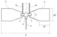
表面側誘電体基板10の表面側には、一対の導体パッチ4,4を軸対象に設けて放射面を形成すると共に、これら一対の導体パッチ4,4の間に配置した3電極高周波増幅素子たる高周波トランジスタ1の制御電極たるゲート電極2および被制御電流流入電極たるドレイン電極3を導体パッチ4,4に各々接続し、ゲート電極2にはゲート直流Bias電圧供給用のRFチョーク回路5aが接続されている。このRFチョーク回路5aには、直流ゲート電圧供給端子15を介して図示を省略した直流電源から給電される。また、ドレイン電極3には、導体パッチ4およびモノパルス信号供給用のRFチョーク回路5bが接続されている。RFチョーク回路5bとベースバンド信号入力端子6との間にモノパルス発生回路7(例えば、高速ロジックICやスイッチにより構成)が直列に接続されている。モノパルス発生回路7のGNDは、内層GND12にスルーホール17で接続されている。高周波トランジスタ1の被制御電流流出電極たるソース電極8には、発振条件を満たすインピーダンス線路9が接続され、内層GND12にスルーホール接地されている。そして、高周波トランジスタ1と導体パッチ4とRFチョーク回路5a,5bの一部とインピーダンス線路9は表面側誘電体基板10の表面(高周波パルス放射側の面)に構成されており、RFチョーク回路5a,5bの残りの部分とモノパルス発生回路7は裏面側誘電体基板11の裏面に構成されている。RFチョーク回路5a,5bにはスルーホール部13が含まれる。
On the surface side of the surface-
ここで、導体パッチ4は、共振器、アンテナとして機能すると共に、帰還回路を構成している。この導体パッチ4の面積・形状設定等と前記高周波トランジスタへの直流給電によりRF信号を発振放射する放射型発振器を実現する。
Here, the
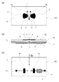
図2は、一対の軸対称な導体パッチ4を示すもので、各導体パッチ4は、高周波トランジスタ1のゲート電極2またはドレイン電極3に接続される等傾斜角の尖鋭部を具備し、これら先鋭部が互いに近接配置され、この先鋭部を経て幅Wが等しくなる平行部の長さをD、一対の導体パッチ4の一方端から他方端までの全体の長さ(全長)をLとする。
FIG. 2 shows a pair of
斯く構成した導体パッチ4において、高周波トランジスタ1のゲート電極2またはドレイン電極3が接続される尖鋭部の広がり角θを調整することで、高周波トランジスタ1と共振器との結合強度を調整でき、また、全長L、幅W、平行部の長さDを適宜に選択することで、発振条件の設定に必要な諸条件の選択の自由度が得られる。また、図示を省略したが、導体パッチ4と内層GND12との間隔h(実質的には、表面側誘電体基板10の厚さ)は、発振波長λの1/15〜1/5倍の間で設定することにより、安定な発振状態を確保できる。なお、導体パッチ4の構成は特に限定されるものではなく、表面側誘電体基板10および内層GND12とで、発振RF信号に適した共振キャビティを構成できれば、如何様な構造でも構わない。共振キャビティの改変例については、後に説明する。
In the
上記のように構成した放射型発振器基板S1を動作させるには、直流ゲート電圧供給端子15に適当な直流バイアス電圧を印加しておき、ベースバンド信号入力端子6にモノパルス発生回路7を動作させるためのベースバンド信号を入力する。モノパルス発生回路7からのモノパルス出力信号がRFチョーク回路5bを通して高周波トランジスタ1のドレイン電極3に入力され、モノパルス出力信号自体が電源電圧となり、高周波トランジスタ1による負性抵抗が短時間生じる。その短時間の負性抵抗と、導体パッチ4と表面側誘電体基板10の構造とにより決まる周波数、帯域幅にて、短時間のRF帯発振放射、すなわち高周波パルス信号の発生放射が行われる。
In order to operate the radiation oscillator substrate S1 configured as described above, an appropriate DC bias voltage is applied to the DC gate
なお、ドレイン電極3にモノパルス信号が入力されている間、発振条件が満たされていれば、直流ゲート電圧供給端子15に印加する直流バイアス電圧は外部電源から供給する必要はなく、自己バイアスによって印加してもよい。例えば、そのゲートのバイアス電圧が0[V]で発振条件を満たすのであれば、直流ゲート電圧供給端子15を内層GNDなどと電気的に接続しての0[V]をゲートに印加すれば、直流バイアス給電用の電源は不要である。
If the oscillation condition is satisfied while the monopulse signal is input to the
上記モノパルス信号の波形には特に制限は無く、矩形波形でもガウシアン波形でも三角波形でもよい。また、その波形の立ち上がり時間に高速性は必要でない。例えば、三角波形を考えた場合、その三角波形信号に、放射させる高周波信号成分が含まれている必要はない。その三角波形の谷から山の頂点に向かう立ち上がりを考えた場合、その頂点より少し手前で発振条件を満たし、その頂点の少し後で発振条件から外れさえすれば、たとえ立ち上がり時間が大きくてもよい。放射させる高周波信号成分は前記負性抵抗と前記共振キャビティの構造によるからである。 The waveform of the monopulse signal is not particularly limited, and may be a rectangular waveform, a Gaussian waveform, or a triangular waveform. Further, high speed is not necessary for the rise time of the waveform. For example, when a triangular waveform is considered, the triangular waveform signal does not have to include a high-frequency signal component to be radiated. When considering the rise from the trough of the triangular waveform to the peak of the mountain, the rise time may be long as long as the oscillation condition is satisfied slightly before the peak and the oscillation condition is deviated slightly after that peak. . This is because the high-frequency signal component to be radiated depends on the structure of the negative resistance and the resonant cavity.
本実施形態に係るX帯パルス信号発生装置を実際に作製し、発生放射させた高周波パルス信号を実測した波形図を図3に示す。図3に示した信号のパルス幅は、約600ピコ秒である。 FIG. 3 shows a waveform diagram in which the X-band pulse signal generator according to the present embodiment is actually manufactured and the high-frequency pulse signal generated and radiated is actually measured. The pulse width of the signal shown in FIG. 3 is about 600 picoseconds.
このように、本実施形態に係るパルス信号発生装置は、単純構造であり、特性のばらつきを抑制し、製造上の高い歩留まりを確保する上で有利であり、高信頼性を確保する上でも有利である。特に、精密で微細な薄膜加工技術を必要とするミリ波帯装置の製造においては、装置が単純構造であることが品質管理上非常に有利となる。 As described above, the pulse signal generator according to the present embodiment has a simple structure, is advantageous in suppressing variation in characteristics, ensuring a high manufacturing yield, and advantageous in ensuring high reliability. It is. In particular, in manufacturing a millimeter-wave band device that requires precise and fine thin film processing technology, it is very advantageous in terms of quality control that the device has a simple structure.
また、波源自体がアンテナとして動作するので、波源とアンテナとの間にインピーダンス整合や帯域制限や郡遅延を考慮する必要が無く、波源が存在する時点で、波源と自由空間との超広帯域整合が確保され、劣化の少ない高周波パルス信号の発生放射が可能となる。 In addition, since the wave source itself operates as an antenna, there is no need to consider impedance matching, band limitation, or group delay between the wave source and the antenna, and when the wave source exists, ultra-wideband matching between the wave source and free space is possible. It is possible to generate and emit a high-frequency pulse signal that is secured and has little deterioration.
また、共振キャビティのQを低く設定しやすく、極めて短いパルス幅の高周波パルス信号発生放射に対応できることから、高性能なUWB装置の実現に好適である。UWB通信装置に応用する場合、短いパルス幅の高周波パルス信号は高伝送レート通信に有利である。インパルス型UWBレーダ装置に応用する場合、短いパルス幅の高周波パルス信号は高分解能距離探知に有利である。 Further, since the resonance cavity Q can be easily set low and can cope with high-frequency pulse signal generation radiation having an extremely short pulse width, it is suitable for realizing a high-performance UWB device. When applied to a UWB communication apparatus, a high-frequency pulse signal having a short pulse width is advantageous for high transmission rate communication. When applied to an impulse type UWB radar apparatus, a high-frequency pulse signal having a short pulse width is advantageous for high-resolution distance detection.
また、アンテナへの給電用伝送線路は存在しないことから伝送損失が存在せず、DC/RF変換効率が高く低消費電力である。さらに、発振するのは極短時間であり、トランジスタは間欠動作で短時間の電流を流すので、超低消費電力となることから、バッテリー動作の携帯機器への応用時は特に有利である。 In addition, since there is no transmission line for feeding power to the antenna, there is no transmission loss, high DC / RF conversion efficiency, and low power consumption. Furthermore, oscillation occurs in a very short time, and since the transistor allows a short-time current to flow in an intermittent operation, the power consumption is extremely low, which is particularly advantageous when applied to a battery-operated portable device.
さらに、従来のCW信号発振回路と高速RFスイッチとを組合せて高周波パルス信号を発生させるよう構成したパルス信号発生装置においては、CW信号発振回路が動作しているために放射UWBスペクトラムの中心にCW信号の漏洩(単一スペクトラム)が現れることが問題となるのに対して、本発明に係るパルス信号発生装置は、そのようなCW信号の漏洩が現れることは原理的に無いので、法律で決められたUWB通信スペクトラムマスク内の帯域を有効利用できるという利点もある。 Further, in a pulse signal generator configured to generate a high-frequency pulse signal by combining a conventional CW signal oscillation circuit and a high-speed RF switch, the CW signal oscillation circuit operates so that the CW signal is centered in the radiation UWB spectrum. Whereas signal leakage (single spectrum) appears to be a problem, the pulse signal generator according to the present invention has no principle that such CW signal leakage appears. There is also an advantage that the band in the specified UWB communication spectrum mask can be effectively used.
また、スイッチ回路による急速放電あるいはベースバンドパルス信号の周波数成分のある部分を共振器やフィルタ回路によって選び出し、高周波パルス信号を発生させるよう構成したパルス信号放射装置においては、その急速放電あるいはベースバンドパルス信号自体に放射する高周波信号数成分があらかじめ含まれている必要がある。よって、スイッチ回路やベースバンドパルス信号発生回路に超高速性が求められ、高コストになるのに対して、本発明に係るパルス信号発生装置は、放射する高周波信号数成分があらかじめ含まれている急速放電やベースバンドパルス信号は必要ないので、設計性がよく、低コスト化に有利である。 In a pulse signal emission device configured to generate a high-frequency pulse signal by selecting a portion having a frequency component of a rapid discharge by a switch circuit or a baseband pulse signal by a resonator or a filter circuit, the rapid discharge or baseband pulse is generated. The number of high-frequency signals to be radiated in the signal itself needs to be included in advance. Therefore, the switching circuit and the baseband pulse signal generation circuit are required to be very fast and expensive, whereas the pulse signal generation device according to the present invention includes the number of high-frequency signals to be radiated in advance. Since rapid discharge and baseband pulse signals are not required, the design is good and the cost is reduced.
このように、本実施形態に係るパルス信号発生装置は、構造の単純な放射型発振器を用いて構成でき、高性能化、小型集積化、設計性容易化、低消費電力化、低コスト化が可能である。 As described above, the pulse signal generation device according to the present embodiment can be configured using a radiation oscillator having a simple structure, and has high performance, small integration, easy design, low power consumption, and low cost. Is possible.
なお、図4に示す放射型発振器基板S1′のように、被制御電流流出電極たるソース電極8にモノパルス信号を供給するよう、モノパルス発生回路7をソース電極8に接続しても良い。この場合、モノパルス発生回路7から負のモノパルス信号を出力すれば、接地電位がソース電極からドレイン電極に変わっただけであり、単に基準電位が異なっただけであるから、パルス信号発生装置として同じ動作をする。また、3電極高周波増幅素子たるトランジスタがN型かP型か、あるいはNPN型かPNP型かにより、モノパルス信号を供給する電極は適宜選択すればよい。
Note that the
次に、図5に基づいて、第2実施形態に係るパルス信号発生装置(ゲートドライブ型高周波パルス信号発生装置)を説明する。 Next, a pulse signal generator (gate drive type high frequency pulse signal generator) according to a second embodiment will be described with reference to FIG.
本実施形態のパルス信号発生装置は、放射型発振器基板S2と、これにベースバンド信号を供給する信号源(図示省略)、直流バイアス給電を行う電源装置(図示省略)から構成される。また、本実施形態のパルス信号発生装置の放射型発振器基板S2は、表面側誘電体基板10と裏面側誘電体基板11の間に接地導体層である内層GND12を介在させた3層基板を用いて必要な回路を構成したもので、表面と内層GND12とで放射型発振器のRF回路部を構成し、内層GND12と裏面とでRFチョーク回路およびベースバンド回路を構成する。なお、図5(a)は放射型発振器基板S2の平面(表面側誘電体基板10の表面)を示し、図5(b)は放射型発振器基板S2の概略縦断面構造を示し、図5(c)は放射型発振器基板S2の底面(裏面側誘電体基板11の裏面)を示す。
The pulse signal generator of this embodiment includes a radiation oscillator substrate S2, a signal source (not shown) for supplying a baseband signal thereto, and a power supply device (not shown) for supplying DC bias power. In addition, the radiation oscillator substrate S2 of the pulse signal generator of the present embodiment uses a three-layer substrate in which an inner layer GND12 that is a ground conductor layer is interposed between the front-
高周波トランジスタ1のゲート電極2には、導体パッチ4およびモノパルス信号供給用のRFチョーク回路5aが接続されている。高周波トランジスタ1のドレイン電極3には、導体パッチ4およびドレイン電圧供給用のRFチョーク回路5bが接続されている。このRFチョーク回路5bには、直流ドレイン供給端子18を介して図示を省略した直流電源から給電される。RFチョーク回路5aとベースバンド信号入力端子6との間には、モノパルス発生回路7が直列に接続されている。高周波トランジスタ1のソース電極8には、発振条件を満たすインピーダンス線路9が接続され、接地されている。高周波トランジスタ1と導体パッチ4とRFチョーク回路5a,5bの一部とインピーダンス線路9は表面側誘電体基板10の表面(高周波パルス放射側の面)に構成されており、RFチョーク回路5a,5bの残りの部分とモノパルス発生回路7は裏面側誘電体基板11の裏面に構成されている。RFチョーク回路5a,5bにはスルーホール部13が含まれる。
A
上記のように構成した放射型発振器基板S2を動作させるには、直流ドレイン電圧供給端子18に適当な直流電圧を印加し、ベースバンド信号入力端子6にモノパルス発生回路7を動作させるためのベースバンド信号を入力する。モノパルス発生回路7からのモノパルス出力信号がRFチョーク回路5aを通して高周波トランジスタ1のゲート電極2に入力され、そのモノパルス信号によりゲートが短時間開き、短時間ドレイン電流が流れ、高周波トランジスタ1による負性抵抗が短時間生じる。その短時間の負性抵抗と、導体パッチ4と表側誘電体基板10の構造とにより決まる周波数、帯域幅にて、短時間のRF帯発振放射、すなわち高周波パルス信号の発生放射が行われる。
In order to operate the radiation oscillator substrate S2 configured as described above, an appropriate DC voltage is applied to the DC drain
なお、本実施形態では、モノパルス信号電圧により高周波トランジスタ1のゲートを開かせるため、無信号時(あるモノパルスと次のモノパルスとの間の時間)にはゲートが閉じた状態(ピンチオフ)になるように、適当なバイアス電圧を設定しておく必要がある。
In this embodiment, since the gate of the high-
上記モノパルス信号の波形には特に制限は無く、矩形波形でもガウシアン波形でも三角波形でもよい。また、その波形の立ち上がり時間に高速性は必要でない。例えば、三角波形を考えた場合、その三角波形信号に、放射させる高周波信号成分が含まれている必要はない。その三角波形の谷から山の頂点に向かう立ち上がりを考えた場合、その頂点より少し手前で発振条件を満たし、その頂点の少し後で発振条件から外れさえすれば、たとえ立ち上がり時間が大きくてもよい。放射させる高周波信号成分は前記負性抵抗と前記共振キャビティの構造によるからである。 The waveform of the monopulse signal is not particularly limited, and may be a rectangular waveform, a Gaussian waveform, or a triangular waveform. Further, high speed is not necessary for the rise time of the waveform. For example, when a triangular waveform is considered, the triangular waveform signal does not have to include a high-frequency signal component to be radiated. When considering the rise from the trough of the triangular waveform to the peak of the mountain, the rise time may be long as long as the oscillation condition is satisfied slightly before the peak and the oscillation condition is deviated slightly after that peak. . This is because the high-frequency signal component to be radiated depends on the structure of the negative resistance and the resonant cavity.
このように、本実施形態に係るパルス信号発生装置は、高周波トランジスタ1に対してゲートの開閉制御が可能であればよいので、上述した第1実施形態に比べて、低出力電力、低ドライブ能力のモノパルス発生回路を用いることができ、簡易な構成で比較的廉価にパルス信号発生装置を実現できる。
Thus, the pulse signal generator according to the present embodiment only needs to be able to control the opening and closing of the gate with respect to the high-
なお、図6に示す放射型発振器基板S2′のように、被制御電流流出電極たるソース電極8に直流を供給するようにしても良い。この場合、ソース電極に負の直流電圧を供給すれば、接地電位がソース電極からドレイン電極に変わっただけであり、単に基準電位が異なっただけであるから、パルス信号発生装置として同じ動作をする。また、3電極高周波増幅素子たるトランジスタがN型かP型か、あるいはNPN型かPNP型かにより、直流を供給する電極は適宜選択すればよい。
Note that a direct current may be supplied to the
また、上述した各実施形態に係るパルス信号発生装置において、放射型発振器を構成するための3電極高周波増幅素子として用いる高周波トランジスタ1は、MOS−FETを含むIG−FET(Insulated Gate FET)、HEMT(High Electron Mobility Transistor)、MESFET(Metal−Semiconductor FET)などの電界効果トランジスタ(FET:Field Effect Transistor)、またはHBT(Hetero−junction Bipolar Transistor)などのバイポーラトランジスタ(BJT:Bipolar Junction Transistor)などで、小さな電圧または電流によって大きな電流を制御する増幅機能を有していれば、その種類は特に限定されるものではない。
In the pulse signal generator according to each of the embodiments described above, the high-
さらに、3電極高周波増幅素子の内部構造も特に限定されるものではなく、ダーリントン接続型トランジスタやカスケード接続型トランジスタのような、単体トランジスタを複数組み合わせた構造の素子でもよい。例えば、ダーリントン接続型トランジスタを用いた場合には、単体のトランジスタでは実現できない高い電流増幅率を得られるという利点がある。 Further, the internal structure of the three-electrode high-frequency amplifying element is not particularly limited, and may be an element having a structure in which a plurality of single transistors are combined, such as a Darlington-connected transistor or a cascade-connected transistor. For example, when a Darlington connection type transistor is used, there is an advantage that a high current amplification factor that cannot be realized by a single transistor can be obtained.
また、上述した各実施形態に係るパルス信号発生装置は、HMIC(混成マイクロ波集積回路:hybrid microwave integrated circuit)で実現してもよいし、MMIC(モノリシックマイクロ波集積回路:Monolithic Microwave integrated circuit)で実現してもよい。また、LTCC(Low Temperature Co−fired Ceramics)などを用いた3次元形態の集積回路で実現してもよい。すなわち、第1〜第2実施形態で示した放射型発振器基板S1〜S2の如く、独立したパーツである高周波トランジスタ1を基板上へ搭載する必要はなく、共振キャビティ(導体パッチなど)と共に同一半導体プロセスで半導体ウェハに3電極高周波増幅素子をモノリシックに作り込むようにしても構わない。特に、ミリ波帯電波は波長が短いことから共振キャビティのサイズも小さくなるので、3電極高周波増幅素子をモノリシックな形態(MMIC)で作り込めば、更なる小型・軽量化を図ることができるし、高精度な半導体プロセス技術により高品位で高い生産性を実現できるという利点もある。
Further, the pulse signal generation device according to each of the above-described embodiments may be realized by an HMIC (hybrid microwave integrated circuit) or an MMIC (monolithic microwave integrated circuit). It may be realized. Further, it may be realized by a three-dimensional integrated circuit using LTCC (Low Temperature Co-fired Ceramics) or the like. That is, unlike the radiation type oscillator substrates S1 and S2 shown in the first and second embodiments, it is not necessary to mount the
また、上述した各実施形態に係るパルス信号発生装置において、RFチョーク回路の機能は、RF信号が直流電源側やモノパルス発生回路7側に漏れるのを防ぐ事であるが、たとえRF信号が漏れたとしても、その漏れによる損失を上回る負性抵抗を高周波トランジスタ1により得ることができれば、放射型発振器は動作可能である。よって、RFチョーク回路を設けない放射型発振器により本発明を構成しても、パルス信号発生装置を実現でできる。また、モノパルス発生回路7自体がRF帯にて高インピーダンスの回路であれば、モノパルス発生回路7と放射型発振器とを直接集積化することができ、RFチョーク回路は不要である。また、RFチョーク回路を構成するために、3層基板構造の放射型発振器基板を用いる必要もない。
In the pulse signal generator according to each of the above-described embodiments, the function of the RF choke circuit is to prevent the RF signal from leaking to the DC power source side or the
また、上述した各実施形態における放射型発振器のモノパルス発生回路7としては、高速ロジックICやスイッチの他、Step Recovery Diode(SRD)やNonlinear Transmission Line(NLTL)による回路などで構成できる。SRDやNLTLにより構成したモノパルス発生回路は、直流電源を不要とすることができるので、高周波トランジスタ1を自己バイアス化することなどによりゲートバイアス電圧の供給も省略すれば、直流電源の存在なしに動作する高周波パルス信号発生装置を実現することができる。その場合のパルス信号発生装置は、直流電源も局部発振器も存在しないにもかかわらず、ベースバンド信号からRF帯の高周波パルス信号に信号を変換する周波数アップコンバータのごとき動作となり、単純で使い勝手のよい構成となる。
In addition, the
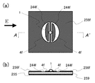
また、上述した各実施形態に係るパルス信号発生装置においては、放射型発振器基板Sに一対の略扇形導体パッチ4を備えるものとしたが、共振キャビティを構成する導体パッチの形状は特に限定されるものではないし、一対の軸対象な導体パッチを必須とするものでもない。以下、本発明に適用可能な導体パッチの改変例について説明する。
In the pulse signal generator according to each of the embodiments described above, the radiation oscillator substrate S is provided with the pair of substantially fan-shaped
図7は矩形状の導体パッチ4aを軸対象に一対設けた第1改変例で、図8は矩形状の導体パッチ4bを軸対象に一対設けた第2改変例で、図9は、円形の導体パッチ4cを軸対象に一対設けた第3改変例である。その他、三角形などの多角形や、楕円形、扇形などの導体パッチでもよい。図7〜図9には、主な偏波面を表すために、電界の向きを矢印Eで示した。GND導体面255は、導体パッチ4a〜4cにとって、内層GND12に相当する。誘電体基板259は、導体パッチ4a〜4cにとって、表面側誘電体基板10に相当する。導体パッチ4a〜4cおよびGND導体面255、誘電体基板259は、共振キャビティを構成し、発振動作のための帰還回路の一部を構成しているが、その帰還が適切に得られさえすれば、誘電体基板259やGND導体面255は必ずしも設ける必要はない。例えば、導体パッチを板金加工で作製し、その導体パッチ板を保持する機構があれば、誘電体基板259の部分は中空でもよい。また、図10に示す第4改変例のように、上記帰還を促すためのチップキャパシタなどの帰還用部品248を導体パッチ4b上に搭載してもよい。なお、GND導体面255が無い場合の放射は、導体パッチ板の両面方向になされる。
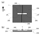
FIG. 7 is a first modified example in which a pair of
図11に示す第5改変例は、略扇形状の導体パッチ4,4の周囲に、GND導体面256と、そのGND導体面256とGND導体面255を接続するスルーホール35を設けて、誘電体基板259内部を信号が伝達して基板の端から漏れ出て損失となるのを防止した例である。GND導体面256の寸法・形状を適当に設定すれば、誘電体基板259内部を信号が伝達する代わりに、その損失分の信号エネルギーを本来の放射エネルギーとして利用できる。
The fifth modified example shown in FIG. 11 is provided with a
図12に示すのは、矩形状の導体パッチ4d,4dと、これら導体パッチ4d,4dと適宜な空隙244を保って配置した接地導体面256dとにより、発振用の共振キャビティを構成した第6改変例である。
FIG. 12 shows a sixth example in which a resonant cavity for oscillation is constituted by
図13に示すのは、高周波トランジスタ1に接続される矩形状の導体パッチ4e1,4e1の付近に、高周波トランジスタ1とは接続されていない矩形状の導体パッチ4e2,4e2を設け、導体パッチ4e1と導体パッチ4e2との間および接地導体面256eとを空隙244eで隔てて、発振用の共振キャビティを構成した第7改変例である。
In FIG. 13, rectangular conductor patches 4e2 and 4e2 not connected to the
図14に示すのは、半楕円状の導体パッチ4f,4fと、これら導体パッチ4f,4fと適宜な空隙244fを保って配置した接地導体面256fとにより、発振用の共振キャビティを構成した第8改変例である。この空隙244fの幅は、場所に応じて変化させ、発振条件を満たすようにする。
FIG. 14 shows a
導体パッチおよび空隙の形状は、上述した図11〜図14に示した構成例に限定されるものではなく、発振条件を満たしていれば、如何様な構成であっても、本発明に適用可能である。また、導体パッチおよび空隙、GND導体面、誘電体基板は、発振動作のための帰還回路の一部を構成しているが、その帰還が適切に得られさえすれば、誘電体基板259やGND導体面255は必ずしも設ける必要はない。なお、GND導体面255が無い場合の放射は、導体パッチ面の両側方向になされる。
The shape of the conductor patch and the gap is not limited to the configuration examples shown in FIGS. 11 to 14 described above, and any configuration can be applied to the present invention as long as the oscillation condition is satisfied. It is. In addition, the conductor patch and the gap, the GND conductor surface, and the dielectric substrate constitute a part of a feedback circuit for the oscillation operation. However, as long as the feedback can be appropriately obtained, the
図15に示すのは、スロット245と接地導体面256とにより発振用の共振キャビティを構成した第9改変例である。このスロット245は、図7にて例示した矩形状の導体パッチ4aに対して、補対の関係にあり、発振条件を満たす。無論、発振条件を満たしていれば、スロット245の形状は特に限定されるものではない。本構成例では、高周波トランジスタ1のゲートとドレインに異なる直流バイアス電圧を印加するために、ゲートとドレインを直流的に分離し、高周波的に導通させる容量結合部246を設けてある。この容量結合部246は、間隙による容量やMIM(Metal−Insulator−Metal)容量、キャパシタ部品などを用いて実現でき、誘電体基板259やGND導体面255は必ずしも設ける必要はない。なお、GND導体面255が無い場合の放射は、導体パッチ面の両側方向になされる。
FIG. 15 shows a ninth modification in which a resonance cavity for oscillation is constituted by the
上述した導体パッチの改変例は、何れも一対の導体パッチを高周波トランジスタ1に対して対象に設けた例を示したが、非対称形状の導体パッチを用いてもよい。
In the above-described modification examples of the conductor patch, an example in which a pair of conductor patches are provided for the high-
図16に示すのは、矩形状の第1導体パッチ4g1と矩形状の第2導体パッチ4g2を非対称に構成した第10改変例である。このように第1導体パッチ4g1と第2導体パッチ4g2を非対称形状としても、共振周波数は導体パッチ部全体の寸法(図16(a)中、Lで示す)で基本的に決まることから、発振条件さえ満たしていれば、アンテナと発振回路が渾然一体となったタイプの放射型発振器として動作させることが可能である。 FIG. 16 shows a tenth modification in which the rectangular first conductor patch 4g1 and the rectangular second conductor patch 4g2 are configured asymmetrically. Thus, even if the first conductor patch 4g1 and the second conductor patch 4g2 are asymmetrical, the resonance frequency is basically determined by the size of the entire conductor patch portion (indicated by L in FIG. 16A). As long as the conditions are satisfied, it is possible to operate as a radiation oscillator of a type in which the antenna and the oscillation circuit are naturally integrated.
図17に示すのは、略半円形の導体パッチ4h,4hと、これら導体パッチ4h,4hと適宜な空隙244hを保って配置した接地導体面256hとにより、リングスロット型アンテナを放射面側に形成し、発振用の共振キャビティを構成した第11改変例である。
FIG. 17 shows a ring slot type antenna on the radiation surface side by substantially
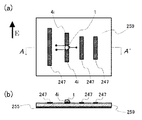
図18に示すのは、矩形状の導体パッチ4、4の周辺に、高周波トランジスタ1と接続されていない導体パッチ247を適宜に配置して、放射指向性を制御可能とした第12改変例である。導体パッチ4i,4iと導体パッチ247との位置関係や、寸法関係を適宜設定することにより、例えば八木アンテナのような動作をさせることができる。
FIG. 18 shows a twelfth modification in which the radiation directivity can be controlled by appropriately arranging the
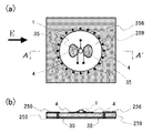
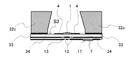
次に、図19に基づいて、第3実施形態に係るパルス信号発生装置を説明する。本実施形態のパルス信号発生装置は、放射型発振器基板S3(上述した放射型発振器基板S1,S1′,S2,S2′と同じ高周波パルス発振・放射構造で、その動作も同じ)に、周波数選択性濾波手段としての周波数選択性平面(FSS:Frequency Selective Surface)を備えたものである。また、放射する高周波パルス信号の周波数より低い周波数の不要信号成分(例えば、ベースバンド信号成分,モノパルス信号成分)の漏洩防止のための接地導体構造を備えたものである。 Next, the pulse signal generator according to the third embodiment will be described with reference to FIG. The pulse signal generator of the present embodiment selects a frequency on the radiation oscillator substrate S3 (the same high-frequency pulse oscillation / radiation structure as that of the radiation oscillator substrates S1, S1 ', S2, and S2' described above, and the operation is the same). It has a frequency selective plane (FSS: Frequency Selective Surface) as a filtering means. In addition, a ground conductor structure is provided for preventing leakage of unnecessary signal components (for example, baseband signal components and monopulse signal components) having a frequency lower than the frequency of the radiated high-frequency pulse signal.
放射型発振器基板S3の放射方向側には、ローパスフィルタパターン30を内面(放射型発振器基板S3の放射面に対向する面)側にパターニングしたFSS基板31が配置され、接地導体構造たる金属導体構造物32aにより放射面から適宜距離を隔てて支持されている。放射型発振器基板S3は、図11に示す第5改変例のように導体パッチ4の周囲を囲むように接地導体ベタパターン33を設け、この接地導体ベタパターン33はスルーホール34で内層GNDと接続されている。なお、スルーホール34は、波長より十分短い間隔で導体パッチの周囲に多数配置されている。
On the radiation direction side of the radiation type oscillator substrate S3, an
上記金属導体構造物32aは、接地導体ベタパターン33を介して内層GNDと電気的に接触しており、直流ないしは比較的低い周波数にとって、金属導体構造物32aは本装置のフレームグランド(本装置全体の基本接地導体)として機能する。また、金属導体構造物32aは、放射型発振器基板S3の放射面側からFSS基板31に向って拡径するホーン形状の放射空部を形成し、高周波パルス信号の放射指向性が鋭くなるようにした。すなわち、金属導体構造物32aは、放射指向性の先鋭化機能とフレームグランドとしての機能を兼務するのである。
The
このように、FSS基板31と金属導体構造物32aを備えた本実施形態の高周波パルス信号発生装置においては、発生した高周波パルス信号の不要な高調波周波数成分をローパスフィルタパターン30にて形成したFSS基板31にて減衰させることができる。さらに、導体パッチ4から漏洩しようとするベースバンド信号およびモノパルス信号成分(直流から比較的低い周波数成分)の電磁界が、導体パッチ4とフレームグランドとの間に閉じ込められて放射には至らない。なお、ベースバンド信号およびモノパルス信号の周波数成分が、高周波パルス信号の周波数成分に対して十分低い場合は、金属導体構造物32aを取り除いて、接地導体ベタパターン33と内層GNDのみでフレームグランドを構成しても、漏洩防止の機能を有する。
As described above, in the high-frequency pulse signal generator of this embodiment including the
また、本実施形態の高周波パルス信号発生装置は、FSS基板31と金属導体構造物32aと放射型発振器基板S3とにより、高周波トランジスタ1と導体パッチ4、4の部分を囲い込んだ形態であり、RF回路部を外気と隔てることができる。よって、FSS基板31と金属導体構造物32aと放射型発振器基板S3とを本装置の気密ハウジングの一部とし、外部環境による性能劣化を防止できる。
In addition, the high-frequency pulse signal generator of the present embodiment has a configuration in which the high-
また、金属導体構造物32aのように、放射空部を放射方向に向って拡径するホーン形状とせずに、図20に示す金属導体構造物32bのように直線管状(第4実施形態)としたり、図21に示す金属導体構造物32cのように放射方向に向かって縮径する形状(第5実施形態)として、その口径の寸法をベースバンド信号およびモノパルス信号の周波数成分がカットオフとなるように設定すれば、ベースバンド信号およびモノパルス信号の不要な漏洩を防止することができる。カットオフとなるように設定するとは、導波管でいうところのカットオフ周波数(低域しゃ断周波数)未満になるよう口径寸法にするということで、カットオフ周波数とは電磁波が管内を管軸方向に進行できなくなる境目の周波数のことである。このようなローカットフィルタは、簡易な構造でありながら、周波数選択性濾波手段の機能と、接地導体構造による不要信号漏洩防止手段の機能とを備えている。
Further, instead of the horn shape in which the radial space is expanded in the radial direction as in the
また、FSS基板31に設ける回路パターンを適宜設定し、発生した高周波パルス信号の基本波周波数成分を減衰させて、任意の高調波周波数成分を選択的に透過させて放射させることもできる。このように高調波周波数成分を不要信号とせずに積極的に利用することで、fmax(最大発振周波数)の小さい低コスト・低性能のトランジスタを用いても、比較的高い周波数のパルス信号放射が可能な装置を実現できる。なお、高調波周波数成分を用いる高周波パルス信号発生装置においては、基本波周波数成分を用いる場合に比べて放射電力が微弱になるものの、近距離通信や近距離センサの信号源として利用できる。
It is also possible to appropriately set a circuit pattern provided on the
なお、本実施形態においては周波数選択性濾波手段としてのFSSを、FSS基板31にFSSパターン面をパターニングして実現したが、FSSパターン面を保持することができれば、特に基板を必要とするものではない。
In this embodiment, the FSS as the frequency selective filtering means is realized by patterning the FSS pattern surface on the
また、FSS以外の周波数選択性濾波手段を採用した第6実施形態のパルス信号発生装置は、図22のように導波管濾波器40を配置したものである。
Moreover, the pulse signal generator of the sixth embodiment that employs frequency selective filtering means other than FSS is one in which a
導波管濾波器40は、放射型発振器の放射波を導波管の伝送波に変換する変換部41と、アイリス板などの導波管回路で構成した濾波器42と、該濾波器42により所望のRF帯域を選別して通過または減衰させ、通過した信号を放射させるホーンアンテナ43を備える。なお、変換部41は、例えばテーパー状構造により所望の大きさの導波管口まで徐々に管の太さを変化させたものであり、仮に放射型発振器基板S3の導体パッチ4が所望の大きさの導波管口より小さいサイズであればテーパー状構造の必要はなく、放射型発振器基板S3からの放射波を導波管の伝送波に効率よく変換できる構造であればよい。
The
以上、本発明に係るパルス信号発生装置を幾つかの実施形態に基づき説明したが、本発明は、これらの実施形態のみに限定されるものではなく、特許請求の範囲に記載の構成を変更しない限りにおいて実現可能な全てのパルス信号発生装置を権利範囲として包摂するものである。 The pulse signal generator according to the present invention has been described above based on some embodiments. However, the present invention is not limited to only these embodiments, and the configuration described in the scope of claims is not changed. All the pulse signal generators that can be realized as far as possible are included in the scope of rights.
上述した特徴的効果を奏する本発明のパルス信号発生装置は、UWB通信システム、UWB車載センサ(レーダ)システム、防犯・医療・看護等のためのUWB電波モニターシステム、UWBアクティブイメージングアレーなどで用いると、上記利点を生かすことができる。特に、部品コストが高く、伝送損失の増加やデバイス性能により低電力効率になるミリ波帯のシステムにおいて大きな優位性が見込まれる。なお、これらのシステムに適用する際には、本発明のパルス信号発生装置をSelf−Oscillatingダウンコンバートミキサとしても動作させれば、同一装置にてインパルス型のUWB送信機とUWB受信機、UWBセンサ装置を実現することができる。例えば、送信機としては、任意のベースバンド信号により任意のタイミングで高周波パルス信号列を発生放射させ、受信機としては、外部からの到来高周波パルス信号が本装置に入射する時にローカル信号に相当する高周波パルス信号を発生すれば、タイミングが合ったときのみダウンコンバート(パルス幅時間内のMixing動作)される信号対雑音比の良好なUWB送受信機、UWBセンサ装置が実現できる。放射指向性を鋭くするには、本装置の放射方向側にホーン構造を設けて所望の開口を確保する方法や、放射PatchあるいはSlotの近くの放射方向側に波面を制御する誘電体レンズを配置する方法などが考えられる。 The pulse signal generator of the present invention that exhibits the above-described characteristic effects can be used in UWB communication systems, UWB in-vehicle sensor (radar) systems, UWB radio wave monitoring systems for crime prevention, medical care, nursing, etc., UWB active imaging arrays, etc. The above advantages can be utilized. In particular, a great advantage is expected in a millimeter wave band system in which the component cost is high and the transmission loss is increased and the device performance is low power efficiency. When applied to these systems, if the pulse signal generator of the present invention is also operated as a Self-Oscillating down-converting mixer, an impulse UWB transmitter, UWB receiver, and UWB sensor can be operated with the same device. An apparatus can be realized. For example, a transmitter generates and radiates a high-frequency pulse signal sequence at an arbitrary timing with an arbitrary baseband signal, and a receiver corresponds to a local signal when an incoming high-frequency pulse signal enters the apparatus. If a high-frequency pulse signal is generated, a UWB transceiver and UWB sensor device having a good signal-to-noise ratio that is down-converted (Mixing operation within the pulse width time) only when the timing is met can be realized. To sharpen the radiation directivity, a horn structure is provided on the radiation direction side of the device to secure a desired opening, or a dielectric lens that controls the wavefront is disposed on the radiation direction side near the radiation patch or slot. Possible ways to do this.
前記UWB通信システムシステムは、家庭やオフィス環境でのPCや周辺機器、AV機器、携帯端末などに本発明に係るパルス信号発生装置で構成したインパルス型UWB送受信機を搭載し、それぞれの機器間のデータ通信を行うシステムである。本システムは、従来のUWB送受信機を用いたシステムに比べ、低コストにて機器間のケーブルレス化を行うことができる。また、低消費電力であることから、特にバッテリーにて動作するノートPCなどの携帯機器に搭載する場合に有利である。 The UWB communication system is equipped with an impulse UWB transceiver configured by the pulse signal generator according to the present invention on a PC, peripheral device, AV device, portable terminal, etc. in a home or office environment. This is a system for data communication. This system can reduce the cable between devices at a lower cost than a system using a conventional UWB transceiver. Further, since it consumes low power, it is particularly advantageous when mounted on a portable device such as a notebook PC that operates on a battery.
前記車載センサシステムは、車体の前後左右に本発明に係るパルス信号発生装置で構成したUWBセンサ装置を複数搭載し、それぞれ適当な変調動作をさせるなどし、その複数のパルス信号発生装置で構成したUWBセンサ装置の中の任意の装置から得たIF信号の位相情報や遅延時間差などを総合的に信号処理、信号解析し、自動制御や運転者への通知などを行うシステムである。これは、単独のセンサ装置を用いた場合に比べ、多角的で正確なセンシングや高解像度センシングが可能であり、また、モーターなどにより機械的にセンサの方角を振る必要が無く、電気的に高速に目標物の方角を特定することも可能である。特に、本発明に係るパルス信号発生装置で構成したUWBセンサ装置は低コスト・低消費電力で提供できるので、多数のセンサ装置を用いた高度な衝突防止等の安全走行機能、車庫入れ時の運転補助機能、車体周囲の死角に起因する事故防止機能などを有する車載センサシステムを普及価格帯にて実現できる。 The in-vehicle sensor system includes a plurality of UWB sensor devices configured by the pulse signal generator according to the present invention on the front, rear, left, and right sides of the vehicle body, each of which performs an appropriate modulation operation, and is configured by the plurality of pulse signal generators. This is a system that performs comprehensive signal processing and signal analysis on the phase information and delay time difference of IF signals obtained from any of the UWB sensor devices, and performs automatic control and notification to the driver. Compared to the case of using a single sensor device, multi-directional and accurate sensing and high-resolution sensing are possible, and there is no need to mechanically swing the direction of the sensor with a motor, etc. It is also possible to specify the direction of the target. In particular, since the UWB sensor device configured with the pulse signal generator according to the present invention can be provided at low cost and low power consumption, it can provide a safe driving function such as advanced collision prevention using a large number of sensor devices, and driving when entering a garage. An in-vehicle sensor system having an auxiliary function, an accident prevention function caused by a blind spot around the vehicle body, and the like can be realized at a popular price range.
前記防犯・医療・看護等のための電波モニターシステムは、住宅の周囲の多数箇所に本発明に係るパルス信号発生装置で構成したUWBセンサ装置を設置し、それぞれの箇所のセンサ装置から得るIF信号から不審な侵入者の存在や場所、移動経路などの情報を警告するシステム、或いは病院内の多数の患者用ベッド上天井部に本発明に係るパルス信号発生装置で構成したUWBセンサ装置をそれぞれ設置してネットワークを構成し、それぞれの患者の存在、呼吸の様子などをモニターし、異常時に警告するシステムなどである。このような多数のセンサ装置を用いるシステムの構築には、単体のセンサ装置が低コストであることが重要であり、本発明のパルス信号発生装置で構成したUWBセンサ装置が有利である。特に、本発明に係るパルス信号発生装置で構成したUWBセンサ装置は、高感度特性であるがゆえに放射電力を弱めて動作させることが可能であり、また、携帯電話などで利用が進んでいる準マイクロ波帯の電波に比べて他の電子機器の動作に与える影響が小さい準ミリ波帯、ミリ波帯の電波を用いるセンサ装置として低コストでの供給を実現できることから、医療機器や心臓ペースメーカなどに誤動作をもたらす外部電波の影響を排除する必要がある病院内において、その有用性は特に高いものである。 The radio wave monitoring system for crime prevention, medical care, nursing, etc. is provided with UWB sensor devices configured by the pulse signal generator according to the present invention at many locations around a house, and IF signals obtained from the sensor devices at the respective locations. A system that warns of information such as the presence and location of suspicious intruders, movement routes, etc., or a UWB sensor device composed of the pulse signal generator according to the present invention is installed on a large number of patient bed ceilings in a hospital. A system that configures a network, monitors the presence of each patient, the state of breathing, etc., and warns when there is an abnormality. For the construction of a system using such a large number of sensor devices, it is important that a single sensor device is low-cost, and a UWB sensor device constituted by the pulse signal generator of the present invention is advantageous. In particular, the UWB sensor device configured with the pulse signal generator according to the present invention has a high sensitivity characteristic, so that it can be operated with weakened radiated power, and is being used in mobile phones and the like. Because it can be supplied at a low cost as a sensor device that uses radio waves in the quasi-millimeter wave and millimeter wave bands, which have a smaller influence on the operation of other electronic devices than microwave waves, such as medical devices and cardiac pacemakers This is particularly useful in hospitals where it is necessary to eliminate the influence of external radio waves that cause malfunctions.
前記アクティブイメージングアレーは、本発明に係るパルス信号発生装置で構成したUWBセンサ装置において、放射型発振器をN行M列のマトリックス状に配置して放射型発振器基板を構成し、マトリックス制御により任意の放射型発振器あるいは全ての放射型発振器を動作・スキャンさせ、それぞれの放射型発振器より取得したIF信号を総合的に信号処理、信号解析することで、被測定物の形状や形状変動などのイメージングを行うものである。 In the UWB sensor device configured by the pulse signal generator according to the present invention, the active imaging array includes a radiation oscillator substrate arranged in a matrix of N rows and M columns, and an arbitrary array is controlled by matrix control. Operate and scan the radiation oscillator or all radiation oscillators, and comprehensively perform signal processing and signal analysis on the IF signals acquired from each radiation oscillator, thereby imaging the shape and shape variation of the object to be measured. Is what you do.
S1,S2,S3 平面放射型発振器基板
1 マイクロ波トランジスタ
2 ゲート
3 ドレイン
4 導体パッチ
5a ゲート側RFチョーク回路
5b ドレイン側RFチョーク回路
6 ドレイン電圧供給端子
7 モノパルス発生回路
8 ソース
9 線路
10 表面側誘電体基板
11 裏面側誘電体基板
12 内層GND
13 スルーホール部
15 直流ゲート電圧供給端子
17 スルーホール
18 ソース電極
S1, S2, S3 Planar emission
13 Through-
Claims (6)
前記3電極高周波増幅素子を短時間動作させることにより短時間の負性抵抗を得て、この負性抵抗と前記共振キャビティの構造に基づいて定まる発振周波数・周波数帯域幅の高周波パルス信号を発生すると同時に空間へ放射するようにしたことを特徴とするパルス信号発生装置。 A three-electrode high-frequency amplifying element is integrated so as to generate a negative resistance in the resonant cavity, and a radiation type oscillator is configured to share an antenna function for radiating electromagnetic waves to space.
When a short-time negative resistance is obtained by operating the three-electrode high-frequency amplifying element for a short time, and a high-frequency pulse signal having an oscillation frequency / frequency bandwidth determined based on the negative resistance and the structure of the resonance cavity is generated A pulse signal generator characterized by radiating into space at the same time.
被制御電流流入電極または被制御電流流出電極にモノパルス信号を供給し、このモノパルス信号自体の電力を電源電力として短時間の負性抵抗を得るようにしたことを特徴とする請求項1に記載のパルス信号発生装置。 The three electrodes in the three-electrode high-frequency amplifying element of the radiation type oscillator are a controlled current inflow electrode, a controlled current outflow electrode, and a control electrode,
The monopulse signal is supplied to the controlled current inflow electrode or the controlled current outflow electrode, and a negative resistance for a short time is obtained using the power of the monopulse signal itself as power supply power. Pulse signal generator.
被制御電流流入電極または被制御電流流出電極に直流を供給し、制御電極にはモノパルス信号を供給することで、短時間の被制御電流が流れるようにし、短時間の負性抵抗を得るようにしたことを特徴とする請求項1に記載のパルス信号発生装置。 The three electrodes in the three-electrode high-frequency amplifying element of the radiation type oscillator are a controlled current inflow electrode, a controlled current outflow electrode, and a control electrode,
By supplying direct current to the controlled current inflow electrode or controlled current outflow electrode and supplying a monopulse signal to the control electrode, a controlled current for a short time flows, and a negative resistance for a short time is obtained. The pulse signal generator according to claim 1, wherein:
Priority Applications (4)
| Application Number | Priority Date | Filing Date | Title |
|---|---|---|---|
| JP2008260816A JP5565823B2 (en) | 2008-10-07 | 2008-10-07 | Pulse signal generator |
| PCT/JP2009/067682 WO2010041752A1 (en) | 2008-10-07 | 2009-10-06 | Pulse signal generation device |
| CN200980144195.4A CN102210060B (en) | 2008-10-07 | 2009-10-06 | Pulse signal generation device |
| US13/123,135 US8847817B2 (en) | 2008-10-07 | 2009-10-06 | Pulse signal generation device |
Applications Claiming Priority (1)
| Application Number | Priority Date | Filing Date | Title |
|---|---|---|---|
| JP2008260816A JP5565823B2 (en) | 2008-10-07 | 2008-10-07 | Pulse signal generator |
Publications (2)
| Publication Number | Publication Date |
|---|---|
| JP2010093491A true JP2010093491A (en) | 2010-04-22 |
| JP5565823B2 JP5565823B2 (en) | 2014-08-06 |
Family
ID=42100698
Family Applications (1)
| Application Number | Title | Priority Date | Filing Date |
|---|---|---|---|
| JP2008260816A Expired - Fee Related JP5565823B2 (en) | 2008-10-07 | 2008-10-07 | Pulse signal generator |
Country Status (4)
| Country | Link |
|---|---|
| US (1) | US8847817B2 (en) |
| JP (1) | JP5565823B2 (en) |
| CN (1) | CN102210060B (en) |
| WO (1) | WO2010041752A1 (en) |
Families Citing this family (9)
| Publication number | Priority date | Publication date | Assignee | Title |
|---|---|---|---|---|
| DE102007034329A1 (en) * | 2007-07-24 | 2009-01-29 | Robert Bosch Gmbh | radar device |
| CN106463834A (en) * | 2014-03-26 | 2017-02-22 | 天线国际有限责任公司 | Patch antenna, method of manufacturing and using such an antenna, and antenna system |
| CN104112899B (en) * | 2014-04-28 | 2017-02-22 | 西安电子工程研究所 | High-power discone antenna |
| GB201503855D0 (en) * | 2015-03-06 | 2015-04-22 | Q Free Asa | Vehicle detection |
| CN106921407B (en) * | 2017-02-28 | 2020-04-21 | 江苏康尔知智能科技有限公司 | Human body tumbling sensing method and device based on UWB automatic detection |
| CN112805878B (en) * | 2018-10-10 | 2022-05-24 | 华为技术有限公司 | Antenna, wireless device and antenna array |
| CN109599679B (en) * | 2018-10-25 | 2020-12-18 | 西安理工大学 | Ultra-wideband frequency selection surface structure applied to ultra-wideband antenna |
| CN110212300B (en) * | 2019-05-22 | 2021-05-11 | 维沃移动通信有限公司 | Antenna unit and terminal equipment |
| CN112615157B (en) * | 2020-12-14 | 2021-10-22 | 西安电子科技大学 | Ultra-wideband pulse radiation antenna applying plane asymptotic conical feed arm |
Citations (13)
| Publication number | Priority date | Publication date | Assignee | Title |
|---|---|---|---|---|
| JPH08511341A (en) * | 1993-04-12 | 1996-11-26 | ザ リージェンツ オブ ザ ユニバーシティ オブ カリフォルニア | Ultra wideband radar motion sensor |
| JPH10511182A (en) * | 1994-12-19 | 1998-10-27 | ザ リージェンツ オブ ザ ユニヴァーシティー オブ カリフォルニア | Impulse radar with swept distance gate |
| JPH1131918A (en) * | 1997-07-11 | 1999-02-02 | Yuseisho Tsushin Sogo Kenkyusho | Microwave and millimeter wave radiation type oscillation device |
| JP2000261234A (en) * | 1999-03-05 | 2000-09-22 | Communication Research Laboratory Mpt | Plate radiation type oscillation device |
| JP2001251138A (en) * | 2000-03-06 | 2001-09-14 | Communications Research Laboratory Mphpt | Planar structure radiating oscillation device |
| JP2004072589A (en) * | 2002-08-08 | 2004-03-04 | Matsushita Electric Ind Co Ltd | Ultra wide band (uwb) transmitter and ultra wide band (uwb) receiver |
| JP2006504963A (en) * | 2002-11-08 | 2006-02-09 | シーメンス アクチエンゲゼルシヤフト | Multi-static sensor device for short-range radar measurement and driving method of the sensor device |
| JP2006074679A (en) * | 2004-09-06 | 2006-03-16 | Futaba Corp | Ultra wideband radio transmitting apparatus, ultra wideband radio receiving apparatus, and ultra wideband radio transmitting/receiving system |
| JP2006112915A (en) * | 2004-10-14 | 2006-04-27 | Anritsu Corp | Short pulse radar |
| JP2007174244A (en) * | 2005-12-21 | 2007-07-05 | Canon Inc | Radio communication equipment and range-finding method |
| JP2007221369A (en) * | 2006-02-15 | 2007-08-30 | Yokohama Rubber Co Ltd:The | Manufacturing method of frequency selective surfaces |
| JP2007318469A (en) * | 2006-05-26 | 2007-12-06 | Murata Mfg Co Ltd | Antenna system and high frequency module |
| JP2008061239A (en) * | 2006-09-01 | 2008-03-13 | Korea Electrotechnology Research Inst | Impulse radio-based ultra wideband communication system using 1-bit high-speed digital sampler and bit decision window |
Family Cites Families (28)
| Publication number | Priority date | Publication date | Assignee | Title |
|---|---|---|---|---|
| DE1466514B2 (en) * | 1965-06-12 | 1970-12-10 | Telefunken Patentverwertungsgesellschaft Mbh, 7900 Ulm | Volume effect oscillator |
| US3626327A (en) * | 1970-06-22 | 1971-12-07 | Litton Precision Prod Inc | Tunable high-power low-noise stabilized diode oscillator |
| US3702977A (en) * | 1971-10-28 | 1972-11-14 | Kjell Olow Ingemar Olsson | Device for generating microwave oscillations |
| US3878480A (en) * | 1973-09-24 | 1975-04-15 | Gen Dynamics Corp | Millimeter wave oscillator with a cavity resonator |
| US4768079A (en) * | 1984-08-07 | 1988-08-30 | M/A Com, Inc. | Field effect transistor device |
| JP2614037B2 (en) * | 1985-06-18 | 1997-05-28 | 財団法人 半導体研究振興会 | Ultra high frequency negative resistance semiconductor oscillator |
| DE3855146T2 (en) * | 1987-06-26 | 1996-08-08 | Texas Instruments Inc | Monolithic microwave transmitter / receiver |
| US4885589A (en) * | 1988-09-14 | 1989-12-05 | General Electric Company | Optical distribution of transmitter signals and antenna returns in a phased array radar system |
| FR2642227A1 (en) * | 1989-01-24 | 1990-07-27 | Labo Electronique Physique | INTEGRATED SEMICONDUCTOR DEVICE INCLUDING BISTABLE ROCKER |
| EP0600118B1 (en) * | 1992-12-01 | 1998-05-27 | Siemens Aktiengesellschaft | Voltage-controlled microwave oscillator |
| US5623233A (en) * | 1993-11-10 | 1997-04-22 | The United States Of America As Represented By The Secretary Of The Army | Pulsed optically injection locked MESFET oscillator |
| CN2245273Y (en) * | 1995-05-15 | 1997-01-15 | 颜夕军 | Automatic control steering antenna |
| US6545553B1 (en) * | 1998-10-08 | 2003-04-08 | Mitel Semiconductor Limited | Oscillator for generating microwave radiation, and method of assembling an oscillator |
| JP3440909B2 (en) * | 1999-02-23 | 2003-08-25 | 株式会社村田製作所 | Dielectric resonator, inductor, capacitor, dielectric filter, oscillator, dielectric duplexer, and communication device |
| AU1922100A (en) | 1999-11-29 | 2001-06-04 | Multispectral Solutions, Inc. | Ultra-wideband data transmission system |
| JP3521834B2 (en) * | 2000-03-07 | 2004-04-26 | 株式会社村田製作所 | Resonator, filter, oscillator, duplexer and communication device |
| JP2003243930A (en) * | 2001-12-12 | 2003-08-29 | Murata Mfg Co Ltd | Oscillator |
| JP4226880B2 (en) | 2002-11-29 | 2009-02-18 | 三星電子株式会社 | Ultra wideband wireless transmitter |
| JP4446785B2 (en) * | 2003-08-27 | 2010-04-07 | 京セラ株式会社 | High-frequency transceiver, radar device including the same, radar device-equipped vehicle equipped with the same, and radar device-equipped small vessel |
| WO2005069905A2 (en) * | 2004-01-16 | 2005-08-04 | Ghz Tr Corporation | Methods and apparatus for automotive radar sensors |
| US7602333B2 (en) * | 2004-02-26 | 2009-10-13 | Kyocera Corporation | Transmitting/receiving antenna, isolator, high-frequency oscillator, and high-frequency transmitter-receiver using the same |
| US7265711B2 (en) * | 2004-06-29 | 2007-09-04 | Kyocera Corporation | High-frequency oscillator, high-frequency transmission-reception apparatus using the same, radar apparatus, and radar-apparatus-equipped vehicle and small boat equipped with the same |
| JP4456998B2 (en) * | 2004-12-28 | 2010-04-28 | 日立オートモティブシステムズ株式会社 | Speed sensor and ground vehicle speed sensor using the same |
| JP2007124628A (en) * | 2005-09-29 | 2007-05-17 | Univ Of Tokyo | Switch/antenna, pulse generator, and associated apparatus |
| JP5196750B2 (en) * | 2006-08-25 | 2013-05-15 | キヤノン株式会社 | Oscillating element |
| EP2144080B1 (en) * | 2007-04-02 | 2020-03-18 | National Institute of Information and Communications Technology | Microwave/millimeter wave sensor apparatus |
| JP5099493B2 (en) | 2007-09-28 | 2012-12-19 | 独立行政法人情報通信研究機構 | Wireless communication network system |
| GB2456043B (en) * | 2007-12-28 | 2011-11-30 | Furuno Electric Co | Harmonic suppression resonator, harmonic propagation blocking filter, and radar apparatus |
-
2008
- 2008-10-07 JP JP2008260816A patent/JP5565823B2/en not_active Expired - Fee Related
-
2009
- 2009-10-06 CN CN200980144195.4A patent/CN102210060B/en active Active
- 2009-10-06 WO PCT/JP2009/067682 patent/WO2010041752A1/en active Application Filing
- 2009-10-06 US US13/123,135 patent/US8847817B2/en active Active
Patent Citations (13)
| Publication number | Priority date | Publication date | Assignee | Title |
|---|---|---|---|---|
| JPH08511341A (en) * | 1993-04-12 | 1996-11-26 | ザ リージェンツ オブ ザ ユニバーシティ オブ カリフォルニア | Ultra wideband radar motion sensor |
| JPH10511182A (en) * | 1994-12-19 | 1998-10-27 | ザ リージェンツ オブ ザ ユニヴァーシティー オブ カリフォルニア | Impulse radar with swept distance gate |
| JPH1131918A (en) * | 1997-07-11 | 1999-02-02 | Yuseisho Tsushin Sogo Kenkyusho | Microwave and millimeter wave radiation type oscillation device |
| JP2000261234A (en) * | 1999-03-05 | 2000-09-22 | Communication Research Laboratory Mpt | Plate radiation type oscillation device |
| JP2001251138A (en) * | 2000-03-06 | 2001-09-14 | Communications Research Laboratory Mphpt | Planar structure radiating oscillation device |
| JP2004072589A (en) * | 2002-08-08 | 2004-03-04 | Matsushita Electric Ind Co Ltd | Ultra wide band (uwb) transmitter and ultra wide band (uwb) receiver |
| JP2006504963A (en) * | 2002-11-08 | 2006-02-09 | シーメンス アクチエンゲゼルシヤフト | Multi-static sensor device for short-range radar measurement and driving method of the sensor device |
| JP2006074679A (en) * | 2004-09-06 | 2006-03-16 | Futaba Corp | Ultra wideband radio transmitting apparatus, ultra wideband radio receiving apparatus, and ultra wideband radio transmitting/receiving system |
| JP2006112915A (en) * | 2004-10-14 | 2006-04-27 | Anritsu Corp | Short pulse radar |
| JP2007174244A (en) * | 2005-12-21 | 2007-07-05 | Canon Inc | Radio communication equipment and range-finding method |
| JP2007221369A (en) * | 2006-02-15 | 2007-08-30 | Yokohama Rubber Co Ltd:The | Manufacturing method of frequency selective surfaces |
| JP2007318469A (en) * | 2006-05-26 | 2007-12-06 | Murata Mfg Co Ltd | Antenna system and high frequency module |
| JP2008061239A (en) * | 2006-09-01 | 2008-03-13 | Korea Electrotechnology Research Inst | Impulse radio-based ultra wideband communication system using 1-bit high-speed digital sampler and bit decision window |
Also Published As
| Publication number | Publication date |
|---|---|
| US8847817B2 (en) | 2014-09-30 |
| US20120002388A1 (en) | 2012-01-05 |
| CN102210060A (en) | 2011-10-05 |
| CN102210060B (en) | 2016-03-30 |
| JP5565823B2 (en) | 2014-08-06 |
| WO2010041752A1 (en) | 2010-04-15 |
Similar Documents
| Publication | Publication Date | Title |
|---|---|---|
| JP5761585B2 (en) | Pulse radar equipment | |
| JP5565823B2 (en) | Pulse signal generator | |
| JP5364921B2 (en) | Pulse radio communication device | |
| US8212718B2 (en) | Microwave/millimeter wave sensor apparatus | |
| TWI278144B (en) | Multibeam antenna | |
| US7239852B2 (en) | Asymmetric, optimized common-source bi-directional amplifier | |
| TWI536660B (en) | Communication device and method for designing multi-antenna system thereof | |
| JP2011509518A (en) | Monolithic integrated antenna and receiver circuit for detecting terahertz waves | |
| Alibakhshikenari et al. | Overcome the limitations of performance parameters of on-chip antennas based on metasurface and coupled feeding approaches for applications in system-on-chip for THz integrated-circuits | |
| WO2010035349A1 (en) | Microwave/millimeter wave communication apparatus | |
| JP2006340202A (en) | Antenna system and wireless communication device comprising the same | |
| Dancila et al. | Differential microstrip patch antenna as feeder of a hyper-hemispherical lens for F-band MIMO radars | |
| JP2006261801A (en) | Multiband compatible microstrip antenna, and module and system employing the same | |
| JP2001053544A (en) | Amplifier module of antenna integrating type | |
| JP2003066133A (en) | Radar | |
| JP2010283500A (en) | Ultra-short pulse generator | |
| JP4911613B2 (en) | Microwave / millimeter wave communication equipment | |
| Zheng et al. | A radiation pattern reconfigurable yagi antenna | |
| EP1036423A2 (en) | Method and arrangement relating to antennas | |
| JP2006054643A (en) | Antenna and radio equipment equipped with antenna | |
| Shinde et al. | Design of Compact UWB Printed Slot Antenna for GPS, GSM &Bluetooth Applications | |
| Qian et al. | Active integrated antennas for microwave front-end technology | |
| JP2005347961A (en) | High frequency flat antenna using dielectric substrate |
Legal Events
| Date | Code | Title | Description |
|---|---|---|---|
| A621 | Written request for application examination |
Free format text: JAPANESE INTERMEDIATE CODE: A621 Effective date: 20111003 |
|
| A131 | Notification of reasons for refusal |
Free format text: JAPANESE INTERMEDIATE CODE: A131 Effective date: 20130730 |
|
| A521 | Written amendment |
Free format text: JAPANESE INTERMEDIATE CODE: A523 Effective date: 20130930 |
|
| A131 | Notification of reasons for refusal |
Free format text: JAPANESE INTERMEDIATE CODE: A131 Effective date: 20140311 |
|
| A521 | Written amendment |
Free format text: JAPANESE INTERMEDIATE CODE: A523 Effective date: 20140512 |
|
| TRDD | Decision of grant or rejection written | ||
| A01 | Written decision to grant a patent or to grant a registration (utility model) |
Free format text: JAPANESE INTERMEDIATE CODE: A01 Effective date: 20140603 |
|
| A61 | First payment of annual fees (during grant procedure) |
Free format text: JAPANESE INTERMEDIATE CODE: A61 Effective date: 20140611 |
|
| R150 | Certificate of patent or registration of utility model |
Ref document number: 5565823 Country of ref document: JP Free format text: JAPANESE INTERMEDIATE CODE: R150 |
|
| S533 | Written request for registration of change of name |
Free format text: JAPANESE INTERMEDIATE CODE: R313533 |
|
| R350 | Written notification of registration of transfer |
Free format text: JAPANESE INTERMEDIATE CODE: R350 |
|
| R250 | Receipt of annual fees |
Free format text: JAPANESE INTERMEDIATE CODE: R250 |
|
| R250 | Receipt of annual fees |
Free format text: JAPANESE INTERMEDIATE CODE: R250 |
|
| LAPS | Cancellation because of no payment of annual fees |