JP2010074506A - Clock regeneration circuit, demodulation circuit, receiving device, wireless communication system, and method of operating clock regeneration circuit - Google Patents
Clock regeneration circuit, demodulation circuit, receiving device, wireless communication system, and method of operating clock regeneration circuit Download PDFInfo
- Publication number
- JP2010074506A JP2010074506A JP2008239378A JP2008239378A JP2010074506A JP 2010074506 A JP2010074506 A JP 2010074506A JP 2008239378 A JP2008239378 A JP 2008239378A JP 2008239378 A JP2008239378 A JP 2008239378A JP 2010074506 A JP2010074506 A JP 2010074506A
- Authority
- JP
- Japan
- Prior art keywords
- phase
- circuit
- signal
- channel
- phase error
- Prior art date
- Legal status (The legal status is an assumption and is not a legal conclusion. Google has not performed a legal analysis and makes no representation as to the accuracy of the status listed.)
- Granted
Links
Images


Abstract
Description
本発明は、クロック再生回路、復調回路、受信機、及び無線通信システム、並びにクロック再生回路の動作方法に係り、特に直交変調方式を用いた復調回路で用いるクロック再生回路に関する。 The present invention relates to a clock recovery circuit, a demodulation circuit, a receiver, a radio communication system, and an operation method of the clock recovery circuit, and more particularly to a clock recovery circuit used in a demodulation circuit using an orthogonal modulation method.
QPSK(Quadrature Phase Shift Keying)、QAM(Quadrature Amplitude Modulation)等の直交変調方式を用いたディジタル無線通信システムでは、通常、受信側の復調回路(復調器)により受信信号を復調する際、その復調に必要なクロック信号(サンプリングクロック)を受信信号から再生するクロック再生回路が用いられている(例えば、特許文献1参照)。 In a digital wireless communication system using a quadrature modulation method such as QPSK (Quadrature Phase Shift Keying) or QAM (Quadrature Amplitude Modulation), the demodulator (demodulator) on the receiving side normally demodulates the received signal. A clock recovery circuit that recovers a necessary clock signal (sampling clock) from a received signal is used (see, for example, Patent Document 1).
図3は、これに関連する復調回路で用いるクロック再生回路の例を示す。なお、以下の説明では、変調方式は、QPSK、QAM等の直交変調方式、復調器の検波方式は、同期検波方式を想定し、互いに直交するベースバンド成分である同相(In−phase)及び直交(Quadrature)成分の表記として一般的なIch(Iチャンネル)、Qch(Qチャンネル)という表記を用いる。 FIG. 3 shows an example of a clock recovery circuit used in a demodulation circuit related to this. In the following description, the modulation method is assumed to be a quadrature modulation method such as QPSK or QAM, and the detection method of the demodulator is assumed to be a synchronous detection method, and in-phase and quadrature which are baseband components orthogonal to each other. The general notation of Ich (I channel) and Qch (Q channel) is used as the notation of (Quadrature) component.
図3に示すクロック再生回路は、直交復調器1と、発振器2と、Ich用、Qch用アナログ/ディジタル変換器(以下、A/D(Ich)3、A/D(Qch))4と、位相検出器(位相比較器とも言う。)(以下、CLK PD)5と、ループフィルタを構成するローパスフィルタ(以下、CLK LPF)6と、発振器7とを有する。このうち、A/D(Ich)3、A/D(Qch)4、CLK PD5、CLK LPF6、発振器7は、PLL(Phase Locked Loop:位相同期ループ)回路を構成している。
The clock recovery circuit shown in FIG. 3 includes a
直交復調器1は、発振器2からの局部発振信号fc102に基づいて、高周波の受信信号から周波数変換された中間周波数信号IFIN101を、ベースバンド信号の互いに直交する2つのアナログ信号Ich103、Qch104に復調する。
Based on the local oscillation signal fc102 from the
A/D(Ich)3は、発振器7からのサンプリングクロック114に基づいて、直交復調器1により復調されたアナログ信号Ich103をサンプリングしてディジタル信号Ich105に変換する。同様に、A/D(Qch)4も、発振器7からのサンプリングクロック114に基づいて、直交復調器1により復調されたアナログ信号Qch104をサンプリングしてディジタル信号Qch106に変換する。
A / D (Ich) 3 samples
CLK PD5は、A/D(Ich)3、A/D(Qch)4により変換されたディジタル信号Ich105、Qch106の位相誤差をそれぞれ検出する。CLK PD5は、例えば図4に示すようなアイパターン(アイダイアグラム)において、Zero−Cross(ゼロクロス)を検出する方式により、A/D(Ich)3とA/D(Qch)4でのサンプリング位相の最適点(アイの開口部)からのずれ、つまり、位相誤差を検出し、その位相誤差信号112を出力する。 CLK PD5 detects the phase errors of digital signals Ich105 and Qch106 converted by A / D (Ich) 3 and A / D (Qch) 4, respectively. CLK PD5 is a sampling phase at A / D (Ich) 3 and A / D (Qch) 4 by detecting Zero-Cross (zero cross) in an eye pattern (eye diagram) as shown in FIG. The deviation from the optimum point (eye opening), that is, the phase error is detected, and the phase error signal 112 is output.
図4は、CLK PD5における位相誤差の検出方法の一例を示す。同図に示すアイの開口部に対応する(1)から(3)までのサンプリングポイントにおいて、(1)と(3)の極性が異なれば、アイの開口部からの位相誤差を検出できる。すなわち、(1)と(3)の極性が逆であることが位相情報検出条件となる。この条件を満たし、さらに、(2)と(3)の極性が一致していれば、位相遅れ、(2)と(3)の極性が不一致ならば、位相進み等のようにして、アイの開口部からの位相誤差を検出できる。 FIG. 4 shows an example of a method for detecting a phase error in CLK PD5. If the polarities of (1) and (3) are different at the sampling points (1) to (3) corresponding to the eye opening shown in the figure, the phase error from the eye opening can be detected. That is, the phase information detection condition is that the polarities of (1) and (3) are opposite. If this condition is satisfied, and the polarities of (2) and (3) match, the phase is delayed, and if the polarities of (2) and (3) do not match, the phase advance etc. A phase error from the opening can be detected.
CLK LPF6は、CLK PD5が出力した位相誤差信号112から高周波成分を取り除き、位相誤差積算信号113を出力する。
The CLK LPF 6 removes a high frequency component from the phase error signal 112 output from the
発振器7は、位相誤差積算信号113の値に応じた周波数のクロックを、サンプリングクロック114として、A/D(Ich)3とA/D(Qch)4へそれぞれ供給する。
上述した関連技術のクロック再生回路において、CLK PD5では、位相誤差を検出するためには、図4に示す位相情報検出条件を満たす必要があるため、常時、位相誤差が検出できているとは限らない。そのために、CLK PD5では、Ich103とQch104のうち位相検出条件を満たす方のチャンネルを常時選んで、位相誤差信号112として出力していた。したがって、クロック再生回路では、2つのPLL、すなわちIch側ではA/D(Ich)3−CLK PD5−CLK LPF6−発振器7で構成されるPLLが、Qch側ではA/D(Qch)4−CLK PD5−CLK LPF6−発振器7で構成されるPLLがそれぞれ存在していた。
In the related art clock recovery circuit described above, in order to detect the phase error in CLK PD5, it is necessary to satisfy the phase information detection condition shown in FIG. 4, and therefore it is not always possible to detect the phase error. Absent. Therefore, in the
この場合、直交復調器1からA/D(Ich)3までの距離と直交復調器1からA/D(Qch)4までの距離とがほぼ同じであれば、Ich103、Qch104のアイの開口部の位相がほぼ同じであるため、問題なく、PLL回路として動作する。しかし、直交復調器1からA/D(Ich)3までの距離と直交復調器1からA/D(Qch)4までの距離とが異なるような場合には、Ich103とQch104との間に電気長差が発生してしまう。
In this case, if the distance from the
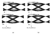
図5は、Ich103とQch104の間に電気長差がある場合のA/D(Ich)3、A/D(Qch)4の入力波形のアイパターンを示し、(a)は、Qchの位相が進んでいる場合、(b)は、Qchの位相が遅れている場合にそれぞれ対応する。同図(a)及ぶ(b)に示すように、Ich103とQch104の間に電気長差がある場合は、信号の収束する(以降、アイが開く)ポイントが、Ich103とQch104で異なってしまう。その結果、Ich103、Qch104のアイの開口部がずれてしまうために、A/D(Ich)3、A/D(Qch)4において、Ich103、Qch104をそれぞれでの最適点でサンプリングすることができず、受信信号の品質が劣化するといった問題があった。
FIG. 5 shows the eye patterns of the input waveforms of A / D (Ich) 3 and A / D (Qch) 4 when there is an electrical length difference between
本発明は、このような課題を解決し、直交復調器から互いに直交する2つのベースバンド成分であるI、Qチャンネルを入力とするA/D変換器までの距離が異なる場合でも、受信信号の品質劣化を抑制することができるクロック再生回路、復調回路、及び無線通信システムを提供することを目的とする。 The present invention solves such a problem, and even when the distance from the quadrature demodulator to the A / D converter that receives two baseband components I and Q, which are orthogonal to each other, is different, An object of the present invention is to provide a clock recovery circuit, a demodulation circuit, and a wireless communication system that can suppress quality degradation.
上記目的を達成するため、本発明に係るクロック再生回路は、受信信号から互いに直交するベースバンド成分であるI及びQチャンネルを復調する直交復調器と、前記I及びQチャンネルをサンプリングクロックに基づいてそれぞれディジタル信号に変換する2つのA/D(Analog to Digital)変換器と、前記2つのA/D変換器の出力信号の位相誤差を検出する位相検出器と、前記位相検出器により検出された位相誤差信号から高周波成分を取り除いて位相誤差積算信号を出力するローパスフィルタと、前記サンプリングクロックとして、前記位相誤差積算信号の値に応じた周波数のクロックを前記2つのA/D変換器にそれぞれ出力する発振器と、前記2つのA/D変換器の出力信号のC/N(Carrier to Noise)推定値をそれぞれ求め、求められた2つのC/N推定値のうちC/N推定値の高いチャンネルに対応するA/D変換器の出力信号の位相誤差を前記位相検出器の位相誤差信号として出力させるC/N推定回路と、前記C/N推定回路により求められたC/N推定値の低いチャンネルに対応するA/D変換器の出力信号の位相を、C/N推定値の高いチャンネルに対応するA/D変換器の出力信号の位相に合わせるように調整する位相調整回路とを備えることを特徴とする。 To achieve the above object, a clock recovery circuit according to the present invention includes a quadrature demodulator that demodulates I and Q channels, which are baseband components orthogonal to each other, from a received signal, and the I and Q channels based on a sampling clock. Two A / D (Analog to Digital) converters that respectively convert to digital signals, a phase detector that detects a phase error in the output signals of the two A / D converters, and the phase detector A low-pass filter that removes high-frequency components from the phase error signal and outputs a phase error integrated signal, and a clock having a frequency corresponding to the value of the phase error integrated signal is output to the two A / D converters as the sampling clock. C / N (Carrier to Noise) estimates of the output signals of the oscillator and the two A / D converters are obtained respectively. A C / N estimation circuit that outputs a phase error of an output signal of an A / D converter corresponding to a channel having a high C / N estimation value of two C / N estimation values as a phase error signal of the phase detector; The phase of the output signal of the A / D converter corresponding to the channel with the low C / N estimation value obtained by the C / N estimation circuit is set to the phase of the A / D converter corresponding to the channel with the high C / N estimation value. And a phase adjustment circuit that adjusts to match the phase of the output signal.
本発明に係る復調回路は、上記に記載のクロック再生回路を有することを特徴とする。 A demodulation circuit according to the present invention includes the clock recovery circuit described above.
本発明に係る受信機は、上記に記載の復調回路を有することを特徴とする。 A receiver according to the present invention includes the demodulation circuit described above.
本発明に係る無線通信システムは、上記に記載の受信機を有することを特徴とする無線通信システム。 A radio communication system according to the present invention includes the receiver described above.
本発明に係るクロック再生回路の動作方法は、直交復調器が、受信信号から互いに直交するベースバンド成分であるI及びQチャンネルを復調し、2つのA/D(Analog to Digital)変換器が、前記I及びQチャンネルをサンプリングクロックに基づいてそれぞれディジタル信号に変換し、位相検出器が、前記2つのA/D変換器の出力信号の位相誤差を検出し、ローパスフィルタが、前記位相検出器により検出された位相誤差信号から高周波成分を取り除いて位相誤差積算信号を出力し、発振器が、前記サンプリングクロックとして、前記位相誤差積算信号の値に応じた周波数のクロックを前記2つのA/D変換器にそれぞれ出力し、C/N推定回路が、前記2つのA/D変換器の出力信号のC/N(Carrier to Noise)推定値をそれぞれ求め、求められた2つのC/N推定値のうちC/N推定値の高いチャンネルに対応するA/D変換器の出力信号の位相誤差を前記位相検出器の位相誤差信号として出力させ、位相調整回路が、前記C/N推定回路により求められたC/N推定値の低いチャンネルに対応するA/D変換器の出力信号の位相を、C/N推定値の高いチャンネルに対応するA/D変換器の出力信号の位相に合わせるように調整することを特徴とする。 In the operation method of the clock recovery circuit according to the present invention, the quadrature demodulator demodulates the I and Q channels, which are baseband components orthogonal to each other, from the received signal, and two A / D (Analog to Digital) converters, The I and Q channels are each converted into a digital signal based on a sampling clock, a phase detector detects a phase error between the output signals of the two A / D converters, and a low-pass filter is converted by the phase detector. A high frequency component is removed from the detected phase error signal to output a phase error integration signal, and the oscillator uses a clock having a frequency corresponding to the value of the phase error integration signal as the sampling clock. And the C / N estimation circuit obtains C / N (Carrier to Noise) estimated values of the output signals of the two A / D converters, respectively. The phase error of the output signal of the A / D converter corresponding to the channel having the higher C / N estimated value of the two C / N estimated values is output as the phase error signal of the phase detector. The phase of the output signal of the A / D converter corresponding to the channel with the low C / N estimation value obtained by the C / N estimation circuit is converted into the A / D converter corresponding to the channel with the high C / N estimation value. The output signal is adjusted so as to match the phase of the output signal.
本発明によれば、直交復調器から互いに直交する2つのベースバンド成分であるI、Qチャンネルを入力とするA/D変換器までの距離が異なる場合でも、受信信号の品質劣化を抑制することができるクロック再生回路、復調回路、及び無線通信システムを提供することができる。 According to the present invention, even when the distance from an orthogonal demodulator to an A / D converter that receives two I and Q channels, which are two baseband components orthogonal to each other, is different, it is possible to suppress the quality deterioration of the received signal. It is possible to provide a clock recovery circuit, a demodulation circuit, and a wireless communication system that can perform the above.
以下、本発明に係るクロック再生回路、復調回路、受信機、及び無線通信システム、並びにクロック再生回路の動作方法の実施形態について、図面を参照して詳細に説明する。 Hereinafter, embodiments of a clock recovery circuit, a demodulation circuit, a receiver, a wireless communication system, and an operation method of the clock recovery circuit according to the present invention will be described in detail with reference to the drawings.
図1は、本実施形態に係るクロック再生回路の構成を示す。このクロック再生回路は、ディジタル無線通信システムの受信機において、QPSK、QAM等の直交変調方式を用いた復調回路に適用したものである。以下の説明では、前述した図3の関連技術と同様に、変調方式は、QPSK、QAM等の直交変調方式、復調器の検波方式は、同期検波方式を想定し、それぞれ直交するベースバンド成分の表記として一般的なIch、Qchという表記を用いる。なお、前述した図3と同様の構成要素については、同一符号を付して説明する。 FIG. 1 shows a configuration of a clock recovery circuit according to the present embodiment. This clock recovery circuit is applied to a demodulation circuit using a quadrature modulation method such as QPSK or QAM in a receiver of a digital radio communication system. In the following description, as in the related art of FIG. 3 described above, the modulation method is assumed to be a quadrature modulation method such as QPSK or QAM, and the detection method of the demodulator is assumed to be a synchronous detection method. As the notation, general notations such as Ich and Qch are used. Note that the same components as those in FIG. 3 described above will be described with the same reference numerals.
図1に示す復調回路で用いるクロック再生回路は、前述した図3の関連技術と同様に、直交復調器1と、発振器2と、2つのA/D、すなわちA/D(Ich)3及びA/D(Qch)4と、CLK PD(位相検出器)5と、ループフィルタを構成するCLK LPF(ローパスフィルタ)6と、発振器7とを有する。本実施形態では、これらの構成要素に加え、位相調整回路8と、C/N(Carrier to Noise ratio:搬送波対雑音比)推定回路9とを有している。
The clock recovery circuit used in the demodulating circuit shown in FIG. 1 is similar to the related art shown in FIG. 3 described above, and includes a
直交復調器1は、発振器2からの局部発振信号fc102に基づいて、高周波の受信信号から周波数変換された中間周波数信号IFIN101を、互いに直交するベースバンド成分であるアナログ信号Ich103、Qch104に復調して出力する。
Based on the local oscillation signal fc102 from the
A/D(Ich)3は、発振器7からのサンプリングクロック114に基づいて、直交復調器1により復調されたアナログ信号Ich103をサンプリングしてディジタル信号Ich105に変換し、CLK PD5に出力する。同様に、A/D(Qch)4も、発振器7からのサンプリングクロック114に基づいて、直交復調器1により復調されたアナログ信号Qch104をサンプリングしてディジタル信号Qch106に変換し、CLK PD5に出力する。
A / D (Ich) 3 samples
C/N推定回路9は、A/D(Ich)3とA/D(Qch)4のサンプリングポイントでの出力信号Ich105、Qch106のC/N推定値を求め、両C/N推定値を比較して、C/N推定値の高い、すなわち収束度の高い方のチャンネルをIch/Qch選択情報116として、CLK PD5と位相調整回路8へそれぞれ出力する。
The C /
CLK PD5は、A/D(Ich)3、A/D(Qch)4により変換されたディジタル信号Ich105、Qch106の位相誤差をそれぞれ検出する。CLK PD5は、例えば図4に示すようなアイパターン(アイダイアグラム)において、Zero−Cross(ゼロクロス)を検出する方式により、A/D(Ich)3とA/D(Qch)4でのサンプリング位相の最適点(アイの開口部)からのずれ、つまり、位相誤差を検出する。 CLK PD5 detects the phase errors of digital signals Ich105 and Qch106 converted by A / D (Ich) 3 and A / D (Qch) 4, respectively. CLK PD5 is a sampling phase at A / D (Ich) 3 and A / D (Qch) 4 by detecting Zero-Cross (zero cross) in an eye pattern (eye diagram) as shown in FIG. Deviation from the optimum point (eye opening), that is, a phase error is detected.
図4は、CLK PD5における位相誤差の検出方法の一例を示す。同図に示すアイの開口部に対応する(1)から(3)までのサンプリングポイントにおいて、(1)と(3)の極性が異なれば、アイの開口部からの位相誤差を検出できる。すなわち、(1)と(3)の極性が逆であることが位相情報検出条件となる。この条件を満たし、さらに、(2)と(3)の極性が一致していれば、位相遅れ、(2)と(3)の極性が不一致ならば、位相進み等のようにアイの開口部からの位相遅れ及び位相進みを検出できる。 FIG. 4 shows an example of a method for detecting a phase error in CLK PD5. If the polarities of (1) and (3) are different at the sampling points (1) to (3) corresponding to the eye opening shown in the figure, the phase error from the eye opening can be detected. That is, the phase information detection condition is that the polarities of (1) and (3) are opposite. If this condition is satisfied and the polarities of (2) and (3) match, the phase is delayed, and if the polarities of (2) and (3) do not match, the eye opening such as phase advance The phase lag and phase lead from can be detected.
本実施形態では、CLK PD5は、A/D(Ich)3、A/D(Qch)4により変換されたディジタル信号Ich105、Qch106の位相誤差をそれぞれ検出し、そのうち、Ich/Qch選択信号116により選択されたC/N推定値の高い方のチャンネル(以降、「選択チャンネル」と呼ぶ。)の位相誤差を、CLK PD5の位相誤差信号112として出力する。また、CLK PD5は、Ich105、Qch106のそれぞれの位相誤差を、Ich位相情報110、Qch位相情報111として、位相調整回路8へ出力する。
In this embodiment, the
位相調整回路8は、CLK PD5より出力されたIch位相情報110、Qch位相情報111を基にして、非選択チャンネルの位相を選択チャンネルの位相に合うように位相の調整を行う。
The phase adjustment circuit 8 adjusts the phase so that the phase of the non-selected channel matches the phase of the selected channel based on the Ich phase information 110 and the Qch phase information 111 output from the
なお、位相調整回路8及びC/N推定回路9は、クロック再生回路が非同期時は動作しない。クロック再生回路の同期・非同期の判断は、復調回路の制御系回路により行う。すなわち、位相調整回路8及びC/N推定回路9は、復調回路のクロック再生回路が、同期している場合にのみに動作する。クロック再生回路の同期/非同期情報は、DEM CLK SYNC信号115より判断する。DEM CLK SYNC信号115は、復調回路の制御系回路(図示しない)より供給される。
The phase adjustment circuit 8 and the C /
CLK LPF6は、CLK PD5が出力した位相誤差信号112から高周波成分を取り除き、位相誤差積算信号113を出力する。
The CLK LPF 6 removes a high frequency component from the phase error signal 112 output from the
発振器7は、位相誤差積算信号113の値に応じた周波数のクロックを、サンプリングクロック114として、A/D(Ich)3とA/D(Qch)4へそれぞれ供給する。 The oscillator 7 supplies a clock having a frequency corresponding to the value of the phase error integration signal 113 to the A / D (Ich) 3 and A / D (Qch) 4 as the sampling clock 114, respectively.
次に、本実施形態の全体動作について説明する。 Next, the overall operation of this embodiment will be described.
まず、クロックの同期の確立は、通常、A/D(Ich)3、A/D(Qch)4、CLK PD5、CLK LPF6、発振器7で構成させるクロック再生回路で行われるが、本実施形態では、新たに位相調整回路8とC/N推定回路9を追加しており、以下にその説明を行う。
First, the synchronization of the clock is normally established by a clock recovery circuit composed of A / D (Ich) 3, A / D (Qch) 4,
発振器2と直交復調器1によって、入力された中間周波数信号IFIN101は、互いに直交する2つのベースバンド信号であるアナログ信号Ich103、Qch104に変換される。変換されたアナログ信号Ich103、Qch104は、A/D(Ich)3、A/D(Qch)4で、それぞれディジタル信号Ich105、Qch106に変換される。変換されたディジタル信号Ich105、Qch106は、CLK PD5において、例えば、図4に示すようなZero−Crossを検出する方式により、A/D(Ich)3とA/D(Qch)4でのサンプリング位相の最適点(アイの開口部)からのずれ、つまり、位相誤差を検出する。
The input intermediate frequency signal IFIN101 is converted by the
ここで、前述した図3の関連技術のクロック再生回路では、CLK PD5において、位相誤差を検出するためには、位相検出条件を満たす必要があるため、常時、位相誤差が検出できているとは限らない。そのために、CLK PD5では、IchとQchで位相検出条件を満たす方を常時選んで、位相誤差信号として出力していた。したがって、クロック再生回路では、A/D(Ich)3−CLK PD5−CLK LPF6−発振器7とA/D(Qch)4−CLK PD5−CLK LPF6−発振器7で構成される2つのPLLが存在していた。 Here, in the clock recovery circuit of the related art shown in FIG. 3 described above, in order to detect the phase error in CLK PD5, it is necessary to satisfy the phase detection condition, so that the phase error can always be detected. Not exclusively. Therefore, in CLK PD5, the one that satisfies the phase detection condition for Ich and Qch is always selected and output as a phase error signal. Therefore, in the clock recovery circuit, there are two PLLs composed of A / D (Ich) 3-CLK PD5-CLK LPF6-oscillator 7 and A / D (Qch) 4-CLK PD5-CLK LPF6-oscillator 7. It was.
この場合、前述したように、直交復調器1からA/D(Ich)3までの距離と直交復調器1からA/D(Qch)4までの距離がほぼ同じならば、Ich、Qchのアイの開口部の位相がほぼ同じであるため、問題なくPLL回路として動作する。しかし、直交復調器1からA/D(Ich)3までの距離と直交復調器1からA/D(Qch)4までの距離が異なるような場合には、前述した図5(a)及び(b)に示す通り、Ich、Qchのアイの開口部がずれてしまう。このために、A/D(Ich)3、A/D(Qch)4において、それぞれの最適点でサンプリングすることができず、受信信号の劣化が生じてしまっていた。
In this case, as described above, if the distance from the
これに対し、本実施形態では、C/N推定回路9において、A/D(Ich)3とA/D(Qch)4のサンプリングポイントでのそれぞれのC/N推定値を求め、IchとQchのC/N推定値の比較を行い、C/N推定値の高い方の選択チャンネルをIch/Qch選択信号116として出力する。CLK PD5では、C/N推定回路9から入力されたIch/Qch選択信号116により、選択チャンネルの位相誤差信号をCLK PD5の位相誤差信号112として出力する。すなわち、A/D(Ich)3、A/D(Qch)4の出力信号の収束度をC/N推定回路9で求めることにより、収束度の高い(C/N推定値の高い)方のチャンネルの位相誤差をCLK PD5の位相誤差信号として、出力とする。
In contrast, in the present embodiment, the C /
これにより、CLK PD5は、Ich/Qch選択信号116により、C/N推定値の高い方の選択チャンネルの位相誤差信号をCLK PD5の位相誤差信号112として出力し、これを基にして、クロック再生回路を動作させる。それにより、選択チャンネルにおいては、常時、アイが開くポイントでサンプリングさせるので、安定した品質の受信信号を得ることができる。 As a result, the CLK PD5 outputs the phase error signal of the selected channel with the higher C / N estimated value as the phase error signal 112 of the CLK PD5 by the Ich / Qch selection signal 116, and based on this, the clock recovery is performed. Operate the circuit. Thus, in the selected channel, sampling is always performed at the point where the eye opens, so that a reception signal with stable quality can be obtained.
すなわち、図3に示す関連技術のクロック再生回路では、A/D(Ich)3−CLK PD5−CLK LPF6−発振器7と、A/D(Qch)4−CLK PD5−CLK LPF6−発振器7で構成される2つのPLLが存在したものが、1つになるため、クロック再生回路の制御が簡素化される。そして、Ich、Qchでそれぞれ存在していた2つのPLLを1つに決めることで、選択チャンネルに関しては、アイが開くポイントで確実にサンプリングすることができる。 That is, the related art clock recovery circuit shown in FIG. 3 includes an A / D (Ich) 3-CLK PD5-CLK LPF6-oscillator 7 and an A / D (Qch) 4-CLK PD5-CLK LPF6-oscillator 7. Since there are only two PLLs to be provided, the control of the clock recovery circuit is simplified. By selecting two PLLs that existed for Ich and Qch as one, it is possible to reliably sample the selected channel at the point where the eye opens.
また、本実施形態では、位相調整回路8では、C/N推定回路9により求められたC/N推定値の低い方の非選択チャンネルの位相を、選択チャンネルの位相に合わせるように制御を行う。この場合、位相調整回路8では、CLK PD5により出力されたIch位相情報110とQch位相情報111を基にして、選択チャンネルのアイの開口部に合うように、非選択チャンネルの位相を調整する。これにより、非選択チャンネルでも、アイの開口部で確実にサンプリングすることができる。なお、位相調整回路8では、CLK PD5より入力されたIch、Qchの位相誤差信号であるIch位相情報110、Qch位相情報111、及びC/N推定回路9より入力されたIch/Qch選択信号116を基にして、位相調整を行う。以下に位相調整の一例を示す。
Further, in the present embodiment, the phase adjustment circuit 8 performs control so that the phase of the non-selected channel with the lower C / N estimation value obtained by the C /
位相調整回路8は、入力されたIch/Qch選択信号116により、IchとQchのどちらが選択チャンネル、又は非選択チャンネルであるかを判断する。選択チャンネル及び非選択チャンネルの位相誤差は、それぞれある一定時間に平均化し、互いに位相比較することで、選択チャンネルに対して、非選択チャンネルの位相が進んでいるか、遅れているかを判断することができる。選択チャンネルに対して、非選択チャンネルの位相が進んでいる場合は遅らせ、遅れている場合は進ませることで、非選択チャンネルの位相を選択チャンネルに近づけることができる。 Based on the input Ich / Qch selection signal 116, the phase adjustment circuit 8 determines which of the Ich and Qch is the selected channel or the non-selected channel. It is possible to determine whether the phase of the non-selected channel is advanced or delayed with respect to the selected channel by averaging the phase errors of the selected channel and the non-selected channel at a certain time and comparing the phases with each other. it can. The phase of the non-selected channel can be made closer to the selected channel by delaying the phase when the phase of the non-selected channel is advanced with respect to the selected channel and by moving the phase when the phase is delayed.
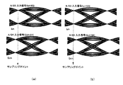
図2は、IchとQchで電気長差がある場合のA/D(Ich)3、A/D(Qch)4の入力波形を示し、(a)は図3の関連技術と同様に位相調整回路8とC/N推定回路9を有しない構成の場合、(b)は本実施形態の位相調整回路8とC/N推定回路9を有する構成の場合にそれぞれ対応する。本実施形態では、クロック再生回路に、位相調整回路8とC/N推定回路9を新たに追加することにより、図2(a)に示す関連技術の場合と比べ、図2(b)に示すように、Ich、Qchともに、アイが開いたポイントでのサンプリングが可能となり、受信信号の品質を向上させることができる。
FIG. 2 shows the input waveforms of A / D (Ich) 3 and A / D (Qch) 4 when there is a difference in electrical length between Ich and Qch, and (a) is the phase adjustment as in the related art of FIG. In the case where the circuit 8 and the C /
従って、本実施形態によれば、直交復調器1からA/D(Ich)3までの距離と直交復調器1からA/D(Qch)4までの距離が異なり、アイの開くポイントがIchとQchで異なる場合においても、クロック再生回路に位相調整回路8とC/N推定回路9を新たに追加することにより、Ich、Qchをそれぞれ最適なポイント(アイが開いたポイント)でサンプリングすることが可能となる。その結果、直交復調器1からA/D3(Ich)までの距離と直交復調器1からA/D4(Qch)までの距離が異なる場合に生じていた受信信号の劣化を防ぐことができ、受信信号の品質を向上させることができる。
Therefore, according to the present embodiment, the distance from the
なお、本発明における復調器の検波方式は、同期検波方式を想定しているが、準同期検波方式においても適用可能である。 Note that the detection method of the demodulator in the present invention assumes a synchronous detection method, but can also be applied to a quasi-synchronous detection method.
本発明は、直交変調方式を用いたディジタル無線通信システム、受信機、復調回路、及びクロック再生回路で利用可能である。 The present invention can be used in a digital radio communication system, a receiver, a demodulation circuit, and a clock recovery circuit using an orthogonal modulation system.
1 直交復調器
2 発振器
3 A/D(Ich)(Ich用アナログ/ディジタル変換器)
4 A/D(Qch)(Qch用アナログ/ディジタル変換器)
5 CLK PD(位相検出器)
6 CLK LPF(ローパスフィルタ)
7 発振器
8 位相調整回路
9 C/N推定回路
1
4 A / D (Qch) (analog / digital converter for Qch)
5 CLK PD (Phase detector)
6 CLK LPF (low pass filter)
7 Oscillator 8 Phase adjustment circuit 9 C / N estimation circuit
Claims (7)
前記I及びQチャンネルをサンプリングクロックに基づいてそれぞれディジタル信号に変換する2つのA/D(Analog to Digital)変換器と、
前記2つのA/D変換器の出力信号の位相誤差を検出する位相検出器と、
前記位相検出器により検出された位相誤差信号から高周波成分を取り除いて位相誤差積算信号を出力するローパスフィルタと、
前記サンプリングクロックとして、前記位相誤差積算信号の値に応じた周波数のクロックを前記2つのA/D変換器にそれぞれ出力する発振器と、
前記2つのA/D変換器の出力信号のC/N(Carrier to Noise)推定値をそれぞれ求め、求められた2つのC/N推定値のうちC/N推定値の高いチャンネルに対応するA/D変換器の出力信号の位相誤差を前記位相検出器の位相誤差信号として出力させるC/N推定回路と、
前記C/N推定回路により求められたC/N推定値の低いチャンネルに対応するA/D変換器の出力信号の位相を、C/N推定値の高いチャンネルに対応するA/D変換器の出力信号の位相に合わせるように調整する位相調整回路とを備えることを特徴とするクロック再生回路。 An orthogonal demodulator that demodulates I and Q channels, which are baseband components orthogonal to each other, from a received signal;
Two A / D (Analog to Digital) converters for converting the I and Q channels into digital signals based on a sampling clock;
A phase detector for detecting a phase error between output signals of the two A / D converters;
A low-pass filter that removes high-frequency components from the phase error signal detected by the phase detector and outputs a phase error integrated signal;
As the sampling clock, an oscillator that outputs a clock having a frequency corresponding to the value of the phase error integration signal to each of the two A / D converters,
C / N (Carrier to Noise) estimated values of the output signals of the two A / D converters are respectively obtained, and A corresponding to a channel having a higher C / N estimated value among the obtained two C / N estimated values. A C / N estimation circuit for outputting a phase error of an output signal of the / D converter as a phase error signal of the phase detector;
The phase of the output signal of the A / D converter corresponding to the channel with the low C / N estimation value obtained by the C / N estimation circuit is set to the phase of the A / D converter corresponding to the channel with the high C / N estimation value. A clock recovery circuit comprising: a phase adjustment circuit that adjusts to match the phase of the output signal.
2つのA/D(Analog to Digital)変換器が、前記I及びQチャンネルをサンプリングクロックに基づいてそれぞれディジタル信号に変換し、
位相検出器が、前記2つのA/D変換器の出力信号の位相誤差を検出し、
ローパスフィルタが、前記位相検出器により検出された位相誤差信号から高周波成分を取り除いて位相誤差積算信号を出力し、
発振器が、前記サンプリングクロックとして、前記位相誤差積算信号の値に応じた周波数のクロックを前記2つのA/D変換器にそれぞれ出力し、
C/N推定回路が、前記2つのA/D変換器の出力信号のC/N(Carrier to Noise)推定値をそれぞれ求め、求められた2つのC/N推定値のうちC/N推定値の高いチャンネルに対応するA/D変換器の出力信号の位相誤差を前記位相検出器の位相誤差信号として出力させ、
位相調整回路が、前記C/N推定回路により求められたC/N推定値の低いチャンネルに対応するA/D変換器の出力信号の位相を、C/N推定値の高いチャンネルに対応するA/D変換器の出力信号の位相に合わせるように調整することを特徴とするクロック再生回路の動作方法。 An orthogonal demodulator demodulates I and Q channels, which are baseband components orthogonal to each other, from a received signal,
Two A / D (Analog to Digital) converters convert the I and Q channels into digital signals based on a sampling clock,
A phase detector detects a phase error between the output signals of the two A / D converters;
A low-pass filter removes high frequency components from the phase error signal detected by the phase detector and outputs a phase error integrated signal,
An oscillator outputs, as the sampling clock, a clock having a frequency corresponding to the value of the phase error integration signal to each of the two A / D converters,
A C / N estimation circuit obtains C / N (Carrier to Noise) estimated values of the output signals of the two A / D converters, and of the obtained two C / N estimated values, the C / N estimated value The phase error of the output signal of the A / D converter corresponding to the high channel is output as the phase error signal of the phase detector,
The phase adjustment circuit converts the phase of the output signal of the A / D converter corresponding to the channel with the low C / N estimation value obtained by the C / N estimation circuit to A corresponding to the channel with the high C / N estimation value. A method for operating a clock recovery circuit, wherein the clock recovery circuit is adjusted to match the phase of the output signal of the / D converter.
Priority Applications (1)
| Application Number | Priority Date | Filing Date | Title |
|---|---|---|---|
| JP2008239378A JP5136854B2 (en) | 2008-09-18 | 2008-09-18 | Clock recovery circuit, demodulation circuit, receiver, radio communication system, and operation method of clock recovery circuit |
Applications Claiming Priority (1)
| Application Number | Priority Date | Filing Date | Title |
|---|---|---|---|
| JP2008239378A JP5136854B2 (en) | 2008-09-18 | 2008-09-18 | Clock recovery circuit, demodulation circuit, receiver, radio communication system, and operation method of clock recovery circuit |
Publications (2)
| Publication Number | Publication Date |
|---|---|
| JP2010074506A true JP2010074506A (en) | 2010-04-02 |
| JP5136854B2 JP5136854B2 (en) | 2013-02-06 |
Family
ID=42205884
Family Applications (1)
| Application Number | Title | Priority Date | Filing Date |
|---|---|---|---|
| JP2008239378A Expired - Fee Related JP5136854B2 (en) | 2008-09-18 | 2008-09-18 | Clock recovery circuit, demodulation circuit, receiver, radio communication system, and operation method of clock recovery circuit |
Country Status (1)
| Country | Link |
|---|---|
| JP (1) | JP5136854B2 (en) |
Cited By (2)
| Publication number | Priority date | Publication date | Assignee | Title |
|---|---|---|---|---|
| WO2011030740A1 (en) * | 2009-09-09 | 2011-03-17 | 日本電気株式会社 | Clock data recovery circuit and clock data recovery method |
| US9886887B2 (en) | 2015-06-26 | 2018-02-06 | Synaptics Japan Gk | Device and method for color reduction with dithering |
Citations (3)
| Publication number | Priority date | Publication date | Assignee | Title |
|---|---|---|---|---|
| JPH07226781A (en) * | 1994-02-15 | 1995-08-22 | Nippon Hoso Kyokai <Nhk> | Phase error detection circuit and clock recovery circuit |
| JPH0897874A (en) * | 1994-09-26 | 1996-04-12 | Toshiba Corp | Offset qpsk demodulator |
| JP2002217880A (en) * | 2001-01-18 | 2002-08-02 | Nec Corp | Circuit and method for synchronizing clock |
-
2008
- 2008-09-18 JP JP2008239378A patent/JP5136854B2/en not_active Expired - Fee Related
Patent Citations (3)
| Publication number | Priority date | Publication date | Assignee | Title |
|---|---|---|---|---|
| JPH07226781A (en) * | 1994-02-15 | 1995-08-22 | Nippon Hoso Kyokai <Nhk> | Phase error detection circuit and clock recovery circuit |
| JPH0897874A (en) * | 1994-09-26 | 1996-04-12 | Toshiba Corp | Offset qpsk demodulator |
| JP2002217880A (en) * | 2001-01-18 | 2002-08-02 | Nec Corp | Circuit and method for synchronizing clock |
Cited By (4)
| Publication number | Priority date | Publication date | Assignee | Title |
|---|---|---|---|---|
| WO2011030740A1 (en) * | 2009-09-09 | 2011-03-17 | 日本電気株式会社 | Clock data recovery circuit and clock data recovery method |
| US8774321B2 (en) | 2009-09-09 | 2014-07-08 | Nec Corporation | Clock data recovery circuit and clock data recovery method |
| US9886887B2 (en) | 2015-06-26 | 2018-02-06 | Synaptics Japan Gk | Device and method for color reduction with dithering |
| US10522068B2 (en) | 2015-06-26 | 2019-12-31 | Synaptics Japan Gk | Device and method for color reduction with dithering |
Also Published As
| Publication number | Publication date |
|---|---|
| JP5136854B2 (en) | 2013-02-06 |
Similar Documents
| Publication | Publication Date | Title |
|---|---|---|
| US8466713B2 (en) | Phase detection method and phase detector | |
| JPH0787149A (en) | Demodulator | |
| EP2645660B1 (en) | Pll circuit | |
| US7492836B2 (en) | Wireless data communication demodulation device and demodulation method | |
| JP2006217054A (en) | Wireless receiver for automatically establishing frequency synchronization or phase synchronization | |
| US5914985A (en) | Digital demodulator | |
| US8861648B2 (en) | Receiving device and demodulation device | |
| JP2007174620A (en) | Psk receiver, psk demodulating circuit, communication apparatus and psk receiving method | |
| JP5136854B2 (en) | Clock recovery circuit, demodulation circuit, receiver, radio communication system, and operation method of clock recovery circuit | |
| US6411658B1 (en) | Demodulation device | |
| US20090268801A1 (en) | Limiter Based Analog Demodulator | |
| JP3489493B2 (en) | Symbol synchronizer and frequency hopping receiver | |
| JP2000138722A (en) | Psk demodulator | |
| JP3518429B2 (en) | Digital PLL device and symbol synchronizer | |
| JPH0897874A (en) | Offset qpsk demodulator | |
| JP2000134271A (en) | Demodulator and demodulation method | |
| JP2003224614A (en) | Digital demodulation circuit | |
| JP4375032B2 (en) | QAM transmission system and QAM receiver | |
| JPH10210095A (en) | Method for correcting frequency error and radio communication equipment | |
| JP3832735B2 (en) | Demodulator circuit | |
| JP3865893B2 (en) | Demodulator circuit | |
| JP2002094480A (en) | Clock signal-regenerating/receiving device, and clock signal reproducing/receiving method | |
| JP4941308B2 (en) | Carrier wave recovery circuit and pseudo pull-in detection method | |
| JP3792477B2 (en) | Frame sync detector | |
| JPH10210092A (en) | Phase detection circuit |
Legal Events
| Date | Code | Title | Description |
|---|---|---|---|
| RD03 | Notification of appointment of power of attorney |
Free format text: JAPANESE INTERMEDIATE CODE: A7423 Effective date: 20100726 |
|
| RD04 | Notification of resignation of power of attorney |
Free format text: JAPANESE INTERMEDIATE CODE: A7424 Effective date: 20100726 |
|
| A621 | Written request for application examination |
Free format text: JAPANESE INTERMEDIATE CODE: A621 Effective date: 20110810 |
|
| A977 | Report on retrieval |
Free format text: JAPANESE INTERMEDIATE CODE: A971007 Effective date: 20120711 |
|
| A131 | Notification of reasons for refusal |
Free format text: JAPANESE INTERMEDIATE CODE: A131 Effective date: 20120723 |
|
| A521 | Written amendment |
Free format text: JAPANESE INTERMEDIATE CODE: A523 Effective date: 20120914 |
|
| TRDD | Decision of grant or rejection written | ||
| A01 | Written decision to grant a patent or to grant a registration (utility model) |
Free format text: JAPANESE INTERMEDIATE CODE: A01 Effective date: 20121018 |
|
| A01 | Written decision to grant a patent or to grant a registration (utility model) |
Free format text: JAPANESE INTERMEDIATE CODE: A01 |
|
| A61 | First payment of annual fees (during grant procedure) |
Free format text: JAPANESE INTERMEDIATE CODE: A61 Effective date: 20121031 |
|
| R150 | Certificate of patent or registration of utility model |
Free format text: JAPANESE INTERMEDIATE CODE: R150 |
|
| FPAY | Renewal fee payment (event date is renewal date of database) |
Free format text: PAYMENT UNTIL: 20151122 Year of fee payment: 3 |
|
| LAPS | Cancellation because of no payment of annual fees |