JP2010072350A - Plastic optical element having fine pattern on optical surface - Google Patents
Plastic optical element having fine pattern on optical surface Download PDFInfo
- Publication number
- JP2010072350A JP2010072350A JP2008239768A JP2008239768A JP2010072350A JP 2010072350 A JP2010072350 A JP 2010072350A JP 2008239768 A JP2008239768 A JP 2008239768A JP 2008239768 A JP2008239768 A JP 2008239768A JP 2010072350 A JP2010072350 A JP 2010072350A
- Authority
- JP
- Japan
- Prior art keywords
- fine pattern
- tip
- plastic
- optical element
- lens
- Prior art date
- Legal status (The legal status is an assumption and is not a legal conclusion. Google has not performed a legal analysis and makes no representation as to the accuracy of the status listed.)
- Granted
Links
Images


Abstract
Description
この発明は光学面に微細パターンを有するプラスチックレンズの光学面に関するものであり、射出成形による成形の形状精度が高く、低コストで製造できるものであり、デジタル複写機、レーザービームプリンター等の光走査光学系に用いられるプラスチック回折レンズ等に利用されるものである。 The present invention relates to an optical surface of a plastic lens having a fine pattern on the optical surface, has high shape accuracy by molding by injection molding, and can be manufactured at low cost. Optical scanning of a digital copying machine, a laser beam printer, etc. It is used for a plastic diffractive lens used in an optical system.
この発明に関連する従来技術として特開2005−258392号公報(特許文献1)に記載されているものがある。これは光走査光学系に回折光学面を有するプラスチックレンズを用いることにより、光学ハウジング内の温度変動による光源波長、屈折率、レンズ面形状、レンズ肉厚の変化を、回折光学面でキャンセルすることが可能であり、これによってピント位置ずれを大幅に低下させることができるものである。 As a prior art related to this invention, there is one described in Japanese Patent Laid-Open No. 2005-258392 (Patent Document 1). By using a plastic lens with a diffractive optical surface in the optical scanning optical system, changes in the light source wavelength, refractive index, lens surface shape, and lens thickness due to temperature fluctuations in the optical housing can be canceled by the diffractive optical surface. Therefore, the focus position deviation can be greatly reduced.
また、他の従来技術として特開2006−323257号公報(特許文献2)に記載されているものがある。これは光学面にグレーティングを有する光学素子に、ハンドリング用の所定寸法のリブを設けることにより、光学面に触れることなく容易にハンドリングすることを可能にしたものである。そして、このことによって光学面に汚れが付着することがなく、また傷つけられることがないようにしている。しかし、これはこの出願の発明とは技術的に全く異質で関わりのないものである。 Another conventional technique is described in JP-A-2006-323257 (Patent Document 2). This is because an optical element having a grating on the optical surface is provided with a rib having a predetermined dimension for handling, thereby enabling easy handling without touching the optical surface. This prevents the optical surface from being contaminated and damaged. However, this is technically quite different from the invention of this application.
ところで、レーザー方式の画像機器(例えばデジタル複写機、プリンターなど)の光走査光学系は、画像の高密度化、高画質化が進み、それに伴い感光体上でのビームスポットをさらに小径化することが求められている。光走査光学系には、レーザービームの結像、及び各種補正機能を有するレンズが用いられている。
ビームスポットの小径化を左右するものの1つにレンズの特性がある。一般的に使用されるガラスレンズでは加工できる形状に限界があり、このため、レンズ面の形状は概ね単純な球面であるのが一般的である。したがって、このガラスレンズに特殊な機能を持たせることは困難であり、これにより、ビームスポットをさらに小径化するのは極めて困難である。
By the way, in the optical scanning optical system of laser-type image equipment (for example, digital copying machines, printers, etc.), the image density and image quality have been improved, and accordingly, the beam spot on the photoconductor is further reduced in diameter. Is required. In the optical scanning optical system, a lens having a laser beam imaging and various correction functions is used.
One of the factors affecting the reduction of the beam spot diameter is the lens characteristic. The glass lens generally used has a limit in the shape that can be processed. Therefore, the shape of the lens surface is generally a simple spherical surface. Therefore, it is difficult to give this glass lens a special function, and it is extremely difficult to further reduce the diameter of the beam spot.
そこで、光走査光学系を構成するレンズをプラスチック化することにより、ビームスポットの小径化を可能にする工夫がなされている。それは、プラスチックは金型のレンズ面を転写して成形されるものであって、所要のレンズ面の形状を有するプラスチックレンズを容易に製造することができるからである。プラスチックレンズの成形方法としては射出成形法が一般的であり、この成形法によれば大量生産が可能であるので、ガラスレンズに比して高性能なプラスチックレンズを低コストで製造することができるというメリットがある。 In view of this, an effort has been made to reduce the diameter of the beam spot by plasticizing the lens constituting the optical scanning optical system. This is because plastic is formed by transferring a lens surface of a mold, and a plastic lens having a required lens surface shape can be easily manufactured. As a method for molding a plastic lens, an injection molding method is generally used. Since this molding method enables mass production, a high-performance plastic lens can be manufactured at a lower cost than a glass lens. There is a merit.
しかし一方で、次のようなデメリットがある。
すなわち、プラスチックは線膨張係数が大きいため、ガラスレンズに比べて温度変化による曲率や寸法の変動が大きく、また、温度変化による屈折率変動も大きい。このような曲率、寸法、屈折率の変動はそのピント位置の変動を生じ、感光体上でのビームスポット径を増大させ、その結果、画像機器の品質を低下させてしまうことになるというデメリットである。
However, there are the following disadvantages.
That is, since plastic has a large coefficient of linear expansion, the variation in curvature and dimensions due to temperature change is larger than that of a glass lens, and the refractive index variation due to temperature change is also large. Such fluctuations in curvature, size, and refractive index cause fluctuations in the focus position, increasing the beam spot diameter on the photoreceptor, and as a result, degrading the quality of the imaging device. is there.
また、温度が変化すると光源である半導体レーザ光の波長も変動する。そして、半導体レーザ光の波長が変動するとこれによってピント位置の変動が生じ、ビームスポット径が増大し、その結果、画像機器の品質が低下してしまうことになる。 Further, when the temperature changes, the wavelength of the semiconductor laser light as the light source also changes. When the wavelength of the semiconductor laser light fluctuates, the focus position fluctuates, and the beam spot diameter increases. As a result, the quality of the image equipment deteriorates.
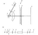
図1に、光走査光学系にプラスチックレンズを用いた場合の従来例(特許文献1の図7と同じ)を示している。図1(a)は、光走査光学系を上から見た平面図であり、図1(b)は、各レンズを直線上に配置して各レンズ面間の距離を表した模式図である。この光走査光学系20は半導体レーザ光の光源11、カップリングレンズ12、アパーチャ13、アナモフィックレンズ14、ポリゴンミラー15、偏向器側走査レンズ16、像面側走査レンズ17、防塵ガラス18、像面19から構成されている。
FIG. 1 shows a conventional example (same as FIG. 7 of Patent Document 1) in which a plastic lens is used in the optical scanning optical system. FIG. 1A is a plan view of the optical scanning optical system as viewed from above, and FIG. 1B is a schematic diagram illustrating the distance between the lens surfaces by arranging the lenses on a straight line. . This optical scanning
光源11から発射された光束は、カップリングレンズ12により弱い発散光となり、アパーチャ13を経て、第1光学系をなすアナモフィックレンズ14を通過する。これによって、主走査方向は平行光となり、副走査方向はポリゴンミラー15近傍に集光する光束となる。さらに、ポリゴンミラー15により偏向され、偏向器側走査レンズ16と、像面側走査レンズ17によって防塵ガラス18を経て画面19に結像する。
The light beam emitted from the
上記特許文献1に、温度による光源波長、屈折率、レンズ面形状、レンズ肉厚の変動を考慮に入れて、像面位置に対するピント位置の変動を算出すると、環境温度が25℃から45℃に変化するとき主走査方向に11.6mm、副走査方向に3.3mmとなり、大きく変動することが記載されている。
そして、上記課題を解決するための発明が特許文献1に記載されている。これはレンズ面に回折光学面を用いて光走査光学系を工夫したものであり、この光走査光学系を図2(特許文献1の図1と同じ)に示している。図2の光走査光学系10は、光源1、カップリングレンズ2、アパーチャ3、アナモルフィックレンズ4、ポリゴンミラー5、偏向器側走査レンズ6、画像側走査レンズ7、防塵ガラス8、像面9等によるものであり、レンズが全てプラスチック製で、カップリングレンズ2の光源側のレンズ面と、アナモフィックレンズ4の像面側レンズ面に回折光学面を用いている。
In the
An invention for solving the above problem is described in
上記回折光学面は、通常の屈折面とは波長変化による屈折角の変化方向が逆であり、この特性を利用すると、温度変化によるピント位置ずれを、回折光学面でキャンセルすることができ、その結果、ピント位置ずれが生じることなく、ビームスポットの小径化が図られる。 The above-mentioned diffractive optical surface is opposite to the normal refractive surface in the direction of change of the refraction angle due to the wavelength change. By utilizing this characteristic, the focus position shift due to the temperature change can be canceled by the diffractive optical surface. As a result, the beam spot can be reduced in diameter without causing a focus position shift.
因みに特許文献1の記載によれば、温度による光源波長、屈折率、レンズ面形状、レンズ肉厚の変動を考慮に入れて、像面位置に対するピント位置の変動を算出すると、環境温度が25℃から45℃に変化に対して主走査方向に−0.2mm、副走査方向に0.0mmとなり、ほとんど変動しないことが分かる。
Incidentally, according to the description in
〔従来技術の問題点〕
ところが、回折光学面を有するプラスチックレンズを製造するについては、下記に示すような製造上の問題(1)、(2)がある。
(1)離型抵抗による回折光学面の形状精度が低下する問題
プラスチックレンズの製造方法としては、大量生産に適していて製造コストが低い射出成形法を用いるのが一般的である。射出成形法は加熱溶融したプラスチック材料を一定温度に保持された成形金型のキャビティに射出して充填し、これを冷却固化させた後、金型から離型させて取り出すという方法である。成形金型の温度制御方法としては、ヒータにより金型温度を制御する方法や、金型に設けた流路内に油や水を循環させて制御する方法などがある。
[Problems of the prior art]
However, manufacturing plastic lenses having diffractive optical surfaces has the following manufacturing problems (1) and (2).
(1) Problem that shape accuracy of diffractive optical surface decreases due to mold release resistance As a method for manufacturing a plastic lens, an injection molding method that is suitable for mass production and low in manufacturing cost is generally used. The injection molding method is a method in which a heated and melted plastic material is injected and filled into a cavity of a molding die maintained at a constant temperature, and after cooling and solidifying it, it is released from the die and taken out. As a method for controlling the temperature of the molding die, there are a method of controlling the die temperature with a heater, a method of controlling oil and water by circulating in a flow path provided in the die, and the like.
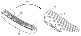
また、プラスチックレンズの外形寸法の大きさの如何が射出成形のサイクルタイムに影響し、成形品の製造コストに大きな影響を与え、その外形寸法が大きいほどサイクルタイムが長くなるが、プラスチックレンズを高精度で成形するならば射出成形のサイクルタイムがさらに長くなる。そこで、射出成形のサイクルタイムを短縮するために、プラスチックレンズの光束が透過しない周縁領域を小さくなるようにプラスチックレンズの形状を設計することが有効である。図3に、回折光学面を有したプラスチックレンズの外形形状を示し、図4に回折光学面側から見た光束透過領域を一点鎖線で示している。図4に示す回折光学面は楕円形状の微細パターンがプラスチックレンズの厚さ方向にステップ状に形成されており、その微細パターンの両側端がレンズ側面と交差している。 In addition, the size of the outer dimensions of the plastic lens affects the cycle time of injection molding, which greatly affects the manufacturing cost of the molded product. The larger the outer dimension, the longer the cycle time. If molding is performed with accuracy, the cycle time of injection molding is further increased. Therefore, in order to shorten the cycle time of injection molding, it is effective to design the shape of the plastic lens so as to reduce the peripheral region where the light flux of the plastic lens does not pass. FIG. 3 shows an outer shape of a plastic lens having a diffractive optical surface, and FIG. 4 shows a light beam transmission region viewed from the diffractive optical surface side by a one-dot chain line. On the diffractive optical surface shown in FIG. 4, an elliptical fine pattern is formed in a step shape in the thickness direction of the plastic lens, and both ends of the fine pattern intersect the lens side surface.
因みに、図4の従来のプラスチック回折レンズはシクロオレフィン樹脂製で、その外形寸法が幅5mm、長さ18mm、長さ方向両端におけるその厚さが 2mmである。そしてまた、これは射出成形されるので、左右両側面は例えば2〜5度の抜き勾配が付けられた傾斜面である。この抜き勾配によって、型抜き抵抗が低減され、型抜き抵抗による成形品の歪み(微細パターンの側縁の変形)が低減される。 Incidentally, the conventional plastic diffractive lens of FIG. 4 is made of cycloolefin resin, and its outer dimensions are 5 mm in width, 18 mm in length, and 2 mm in thickness at both ends in the length direction. And since this is injection-molded, the left and right side surfaces are inclined surfaces with a draft of 2 to 5 degrees, for example. Due to this draft, the punching resistance is reduced, and distortion of the molded product due to the punching resistance (deformation of the side edge of the fine pattern) is reduced.
以上のようなプラスチック回折レンズを射出成形すると、その回折光学面の微細パターンの先端部75において設計形状に対する成形品の形状誤差が大きくなるという現象(形状精度の低下)が見られる。この現象を詳細に解析することにより、形状精度が低下する原因を解明することができた。その原因は次のようである。
When the plastic diffractive lens as described above is injection-molded, a phenomenon (decrease in shape accuracy) in which the shape error of the molded product with respect to the design shape becomes large at the
すなわち、射出成形法では、加熱溶融されたプラスチック材料が比較的低温の金型のキャビティ内に充填され、金型に接したときこの部分が急冷される。特に成形品の薄肉の部分では、そのプラスチック材料が高圧下で急冷されるため、内部歪みが大きくなり高密度化する。そのため、金型キャビティ内のプラスチック材料全体を軟化温度以下に冷却して固化させると、金型から離型する際、そのプラスチック回折レンズ71の微細パターンの先端部75の高密度化した部分(薄肉になっている部分)で、プラスチック材料と金型との離型抵抗が大きく、そのためにこの部分が微小に変形すること(プラスチック材料がめくれ上がる現象)がある(図5参照)。また、上記先端部75はその先端eが薄肉であるので剛性が小さく、当該先端eにおいて設計形状に対する成形品の形状誤差が大きくなるという形状精度の低下が見られる。そして、上記のように形状精度が低い回折光学面72を有するプラスチック回折レンズを用いると、その光走査光学系ではビームスポット径が大きくなってしまう。これが問題(1)である。
That is, in the injection molding method, the plastic material heated and melted is filled in a cavity of a relatively low temperature mold, and this portion is rapidly cooled when it comes into contact with the mold. In particular, in the thin part of the molded product, the plastic material is rapidly cooled under high pressure, so that the internal strain increases and the density increases. For this reason, if the entire plastic material in the mold cavity is cooled to a softening temperature or lower and solidified, when the mold is released from the mold, the
(2)離型抵抗による光学面の微細パターンの先端部の先端が金型内面に付着してしまう問題
ところで、プラスチックレンズを射出成形法で成形すれば大量生産が可能で、複雑な表面形状を備えた高性能プラスチックレンズを低コストで製造することができる。しかし、プラスチックレンズが回折光学面を有するレンズ(プラスチック回折レンズ)である場合は、回折光学面の微細パターンの先端部75の先端(又はエッジ)eの離型抵抗が大きく、また、先端部75の角度αが小さくて先端eが薄肉になっているとき(図3、図4参照)、この薄肉の部分の剛性が低い場合があり、この場合に、図6に示すように、回折光学面72の微細パターンの先端部75の先端eが完全に離型せずにその一部が剥離し、これが金型内面に付着してしまうことがある。このような現象が生じると、射出成形を継続することは不可能になり、金型を分解して上記プラスチック材料を除去し洗浄する必要がある。それゆえ、金型メンテナンスの回数が多くなって、サイクルタイムが大きく損なわれ、また、メンテナンスコストが高くなる。これが問題(2)である。
(2) The problem of the tip of the fine pattern on the optical surface sticking to the inner surface of the mold due to mold release resistance By the way, if plastic lenses are molded by injection molding, mass production is possible, and complex surface shapes are required. The provided high performance plastic lens can be manufactured at low cost. However, when the plastic lens is a lens having a diffractive optical surface (plastic diffractive lens), the release resistance of the tip (or edge) e of the
そして、光学面に微細パターンを有するプラスチックレンズの製造上の問題について、プラスチック回折レンズを例示したが、回折光学面のみならず他の微細パターンを有するプラスチックレンズについても同様の問題がある。その他の例としては例えば光学面の微細パターンが鋸歯状のフレネルレンズや、サブ波長レベルのピッチ、深さの溝が形成されていることにより、反射率を大幅に低下させることができる反射防止機能付きプラスチックレンズ等がある。
そこで、この発明は光学面に微細パターンを有するプラスチックレンズについて、金型メンテナンス回数が増えて射出成形のサイクルタイムが損なわれることがなく、高い形状精度で成形できるようにすることを目的とし、そのために、光学面の微細パターンの先端部のプラスチック材料が金型から完全に離型し、また、微細パターンの上記先端部が離型抵抗で変形することのないようにプラスチックレンズの形状を工夫することをその課題とするものである。 Therefore, the object of the present invention is to make it possible to mold a plastic lens having a fine pattern on the optical surface with high shape accuracy without increasing the number of times of mold maintenance and impairing the cycle time of injection molding. Furthermore, the shape of the plastic lens is devised so that the plastic material at the tip of the fine pattern on the optical surface is completely released from the mold, and the tip of the fine pattern is not deformed by mold release resistance. This is the issue.
上記課題を解決するための手段は次のとおりである。
〔手段1〕
手段1は、一方の光学面に微細パターンが形成されたプラスチック光学素子であって、光学面側端部の光束が透過もしくは反射しない領域で、微細パターンと光学面に隣接する光学素子側面とが交差して微細パターンの先端部が形成されているプラスチック光学素子において、上記微細パターンの全ての先端部の角度が45度以上であることである。
Means for solving the above problems are as follows.
[Means 1]
The
また、上記手段1における前記光学面に形成された微細パターンが、回折パターンであることである(請求項2)。
Further, the fine pattern formed on the optical surface in the
さらに上記手段1における光学面に形成された微細パターンが、その断面が三角形の連なりとなる鋸歯状のフレネルパターンであることである(請求項3)。
Further, the fine pattern formed on the optical surface in the
また、上記手段1における光学面に形成された微細パターンが、透過する光束の波長より短い周期をもつ微細パターンであることである(請求項4)。
Further, the fine pattern formed on the optical surface in the
さらに、以上の手段におけるプラスチック光学素子の側面形状が、多面体であることである(請求項5)。 Furthermore, the side surface shape of the plastic optical element in the above means is a polyhedron (Claim 5).
さらに、以上の手段において、前記プラスチック光学素子の側面形状が、平面でかつ輪郭が矩形であることである(請求項6)。 Further, in the above means, the side surface shape of the plastic optical element is a plane and the outline is a rectangle (Claim 6).
また、上記手段1における光学面に形成された微細パターンと光学面に隣接する光学素子側面とが交差して形成される微細パターンの先端部の先端が、光学素子側面に垂直な平面部を有していることである(請求項7)。
In addition, the tip of the fine pattern formed by intersecting the fine pattern formed on the optical surface and the side surface of the optical element adjacent to the optical surface in the
さらに、以上の手段における前記光学面に形成された微細パターンと光学面に隣接する光学素子側面とが交差して形成される微細パターンの先端部の先端が、光学素子側面に垂直で光学面の長さ方向に凸状に屈曲した円弧面であることである(請求項8)。 Furthermore, the tip of the tip of the fine pattern formed by intersecting the fine pattern formed on the optical surface and the side of the optical element adjacent to the optical surface in the above means is perpendicular to the side of the optical element and It is an arc surface bent in a convex shape in the length direction (claim 8).
以上、手段1及びその下位の種々の手段を説明したが、これらは要するに、光学面の微細パターンと光学素子の左右両側面とが交差して形成される微細パターンの先端部の先端を光学素子の側面に直角で光学面に垂直な平面又は曲面にするなどして、その先端部を薄肉の部分がない形状にし、薄肉であることに因る問題、すなわち、離型の際の上記先端部の離型抵抗(先端部の先端と金型内面の離型抵抗)が大きくなるという問題、同先端部の剥離して金型内面に付着するという問題を防止して、上記先端部の形状精度(設計形状に対する成型品の形状上の精度)を高め、金型のメンテナンス頻度が多くなることを回避して、これによって上記課題を解決したものである。
Although the
〔手段2〕
手段2は、一方の光学面に微細パターンが形成されたプラスチック光学素子であって、光学面側端部の光束が透過もしくは反射しない領域で、微細パターンと光学面に隣接する光学素子側面とが交差して形成される微細パターンの先端部が、微細パターンから上方に突出したリブと一体になっていることである(請求項9)。
[Means 2]
The
そして、手段2は上記微細パターンの外周縁に上方に突出したリブを設け、微細パターンの先端部と上記リブとを一体にして、当該先端部の薄肉の先端の急冷速度を緩和してこれが変形する原因、及び同先端が剥離する原因を解消し、また、当該先端部に対する上記リブの補強機能で、上記先端の変形及び剥離を防止して、上記先端部の形状精度を高め、金型のメンテナンス頻度を下げ、これによって上記課題を解決したものである。
The
なお、請求項10に係る発明の手段は、次の実施形態の範囲の発明であるから、ここでの説明は省略する。
In addition, since the means of the invention which concerns on
上記のとおり、この発明によれば、光学面に微細パターンを有するプラスチックレンズを射出成形するについて、その成形サイクルのサイクルタイムを損うことなしに、高い形状精度で能率的に製造することができる。
また、回折パターンを有する高精度のプラスチック回折レンズを光走査光学系に用いることにより、温度変動によるピント位置ずれが生じることはなく、したがって、ビームスポットを小径にした光走査光学系を実現することができる。
また、以上のように、ビームスポットを小径にした光走査光学系を用いた画像形成装置に用いることによって著しく高品質な画像が安定的に形成することができる。
As described above, according to the present invention, when a plastic lens having a fine pattern on an optical surface is injection-molded, it can be efficiently produced with high shape accuracy without impairing the cycle time of the molding cycle. .
In addition, by using a high-precision plastic diffractive lens having a diffraction pattern in the optical scanning optical system, there is no focus position shift due to temperature fluctuations, and therefore an optical scanning optical system with a small beam spot diameter is realized. Can do.
In addition, as described above, a remarkably high quality image can be stably formed by using the image forming apparatus using the optical scanning optical system in which the beam spot has a small diameter.
次いで図面を参照して実施形態1、実施形態2、実施形態3を説明する。
実施形態1はプラスチック回折レンズについての実施形態であり、実施形態2はプラスチックフレネルレンズについての実施形態であり、実施形態3は反射防止機能付きプラスチックレンズについての実施形態である。
Next,
〔実施形態1〕
〔実施形態1の実施例1〕
実施形態1の実施例1を図7に示している。この実施例1は一方の光学面に、中心位置が同じ多数の楕円が階段状に形成された回折光学面72を有している。この実施例1における個々の楕円の微細パターンの段差(高さ)は1.2μmであり、各楕円状微細パターンの楕円形の長軸方向でのピッチは10−200μmである。
そしてこの実施例1では、回折光学面72に形成された微細パターン(微細パターン)と、回折光学面72に隣接する光学素子側面73とが交差して形成される先端部(微細パターンの先端部)75の先端(又はエッジ)eが光学素子側面73に略直角な平面74になっている。この平面74の高さhは1.2μm、幅wは3〜30μmである。高さhは微細パターンの段差に相当する。そして幅wは5μm以上が好ましく、この例では7μmである。
[Embodiment 1]
[Example 1 of Embodiment 1]
Example 1 of
In the first embodiment, a fine pattern (fine pattern) formed on the diffractive
この実施例1のレンズでは、図3の従来のレンズに比して、プラスチック回折レンズの微細パターンの先端部75の先端は薄肉でない。したがって、金型から離型する際の上記先端部75と金型の離型抵抗は大きくなく、また、先端部75の剛性は低くないので、先端部75が変形する(プラスチック材料がめくれ上がる現象)ことはなく、また、プラスチック回折レンズの上記先端部75に離型時の変形による形状誤差が生じることはない。それゆえ、設計形状に対する形状精度(以下、これを単に「形状精度」という)が高いプラスチック回折レンズが製造される。
In the lens of Example 1, the tip of the
また、プラスチック回折レンズの回折光学面72の微細パターンの先端部75には薄肉の先端はない。したがって微細パターンの先端部75の薄肉の先端が剥離して金型内面に付着してしまうようなことはない。したがって、金型を分解してプラスチック材料を除去し洗浄する必要はなく、金型メンテナンスの回数は少なく、メンテナンスコストは低い。
Further, the
実施例1についての実験結果は次のとおりである。
微細パターンと光学素子側面73とが交差して形成される微細パターンの先端部75の角度αと、その形状誤差との関係を調査した。その結果は図8(b)に示すとおりである。
なお、図8(a)に拡大して示す角度αは、微細パターンの先端の角度であり、この角度αは楕円の長軸と短軸の比率によって異なり、楕円よりも長軸/短軸比が1となる円の方が大きい。この実験結果は、1つのプラスチック回折レンズにおける多数の先端部75の内の7点について確認したものであり、その角度αは35度、40度、45度、90度、120度、140度、160度である。
この図8(b)の実験結果は、上記角度αが45度よりも小さくなると形状誤差が1μm以上になり、上記角度がこれよりも小さくなると形状誤差が急激に増大することを示している。また、上記角度αが30度以下では、上記先端部75の先端、すなわち、先端部75の先端eの薄肉の部分(図4参照)が剥離して金型内面に付着してしまう現象がみられる。上記先端eが剥離したあとの上記先端部75の様子を図6に誇張して示している。
The experimental results for Example 1 are as follows.
The relationship between the angle α of the
8A is an angle of the tip of the fine pattern. The angle α depends on the ratio of the major axis to the minor axis of the ellipse, and the major axis / minor axis ratio is larger than that of the ellipse. The circle with 1 is larger. This experimental result was confirmed with respect to 7 points among a large number of
The experimental results in FIG. 8B show that the shape error becomes 1 μm or more when the angle α is smaller than 45 degrees, and the shape error increases rapidly when the angle is smaller than this. When the angle α is 30 degrees or less, the tip of the
図8(b)に示す実験の結果から、高い形状精度(形状誤差が1μm以下)のプラスチック回折レンズを成形するには、上記角度αが45度以上である必要があることがわかる。
そこで、実施例1はプラスチック回折レンズの微細パターンの先端部75の角度αが45度以下のものの先端を光学素子側面に垂直な平面74にして、先端の薄肉な部分(図4のe参照)をなくしている。
上記角度αが45度以下である微細パターンについてその先端の薄肉の部分をなくすればよいのであるが、実施例1では図示の全ての先端部75が45度以下であるからこれら全ての先端部75の先端を光学素子側面に垂直な平面74にしている。
この実施例1の利点は、金型の製作が容易であることである。
From the result of the experiment shown in FIG. 8B, it can be seen that the angle α needs to be 45 degrees or more in order to mold a plastic diffractive lens with high shape accuracy (shape error is 1 μm or less).
Therefore, in the first embodiment, the tip of the
The thin pattern at the tip of the fine pattern having the angle α of 45 degrees or less may be eliminated. In the first embodiment, since all the
The advantage of Example 1 is that the mold can be easily manufactured.
〔実施形態1の実施例2〕
実施形態1の実施例2を図9に示している。この実施例2では回折光学面72の微細パターンと光学素子側面73とが交差して形成される微細パターンの全ての先端部75の先端が、光学面の長さ方向に凸状に屈曲した円弧面94になっており、これによって、先端部75の先端には薄肉の部分は無くなっている。
図9の実施例2のレンズでは光学面の微細パターンの先端部75の先端には薄肉の部分はないので、金型から離型する際の上記先端部75の先端の離型抵抗は大きくなく、上記先端部75が変形(プラスチック材料がめくれ上がる現象)することはない。したがって、回折光学面の先端部の形状精度が高いプラスチック回折レンズが製造される。また、金型メンテナンスの回数は少なく、メンテナンスコストも低い。
この実施例2の利点は、金型の微細パターン端部角の経時的劣化を抑え長寿命で高安定な成形が実施できることである。
[Example 2 of Embodiment 1]
Example 2 of
In the lens of the second embodiment shown in FIG. 9, since there is no thin portion at the tip of the
The advantage of the second embodiment is that long-life and highly stable molding can be performed while suppressing deterioration of the corner angle of the fine pattern of the mold over time.
〔実施形態1の実施例3〕
実施形態1の実施例3を図10に示している。この実施例3では回折光学面に形成された微細パターンと光学素子側面73とが交差して形成される先端部75の先端が、微細パターンから光学素子の厚さ方向に凸状に屈曲した円弧面104になっている。
図10のレンズは、その微細パターンの先端部75の先端に薄肉の部分はないから、上記先端部75の離型抵抗は大きくなく、この離型抵抗による当該先端部75の変形(プラスチック材料がめくれ上がる現象)はない。したがって、微細パターンの先端部75の形状精度が高いプラスチック回折レンズが製造される。また、金型メンテナンスの回数は少なく、メンテナンスコストは低い。
この実施例3の利点は、実施例2と同様であるが,離型抵抗のさらなる低減が期待できることである。
[Example 3 of Embodiment 1]
Example 3 of
The lens shown in FIG. 10 does not have a thin portion at the tip of the
The advantage of the third embodiment is similar to that of the second embodiment, but can be expected to further reduce the mold release resistance.
〔実施形態1の実施例4〕
実施形態1の実施例4を図11に示している。この実施例4では、回折光学面72に形成された微細パターンと光学素子側面73とが交差して形成される先端部75が微細パターンから上方(図面において上方)に突出したリブ114と一体になっている。この実施例4ではリブ114の厚さは1mm、高さは0.2mmであるが、厚さは0.5〜1.5mm、高さは光学面の総高さ(レンズではサグ量という)+0.1mmであればよい。厚さが0.2以下ではそれ自体が離型抵抗となり、2mm以上では素子が不要に大きくなるので不利である。
[Example 4 of Embodiment 1]
Example 4 of
図11に示すレンズは、光学面周縁にリブ114が上方に突出していて、微細パターンの先端部75が上記リブ114と一体であるから、先端部75が金型に接触したときの急冷速度が緩和される。したがって、先端部75の角度は45度以下でその先端eは薄肉であるが、これが金型から離型する際のその離型抵抗は大きくなく、また、上記リブ114で補強されているから先端部75の先端eの剛性は低くない。したがって、図3の従来例の先端部75の先端eのような変形(図5参照)は防止される。
In the lens shown in FIG. 11, the
なお、上記角度αが45度以下である先端部75に上記リブ114を付設すればよく、実施例4では図示の全ての先端部75の角度αが45度以下であるので、全ての先端部75についてリブ114を付設している。仮に上記角度αが45度以上の先端部75があるとしても、形状のバランス、冷却速度のバランスを図るために、レンズの全周縁にリブ114を付設するのがよい。
以上のとおりであるから、微細パターンの先端部75の形状精度が高いプラスチック回折レンズが製造され、また、金型メンテナンスの回数も少なく、メンテナンスコストも低い。
The
As described above, a plastic diffractive lens with high shape accuracy of the
〔実施形態1の実施例5〕
実施形態1の実施例5を図12に示している。この実施例5では回折光学面72に形成された微細パターンと光学素子側面73が交差して形成される先端部75の先端(又はエッジ)の形状がレンズ厚さ方向に傾斜した傾斜面124になっている。
図12のレンズは、微細パターンの先端部75がレンズ厚さ方向に傾斜した傾斜面であるので、金型の製作が容易であり、射出成形金型から離型する際の、上記先端部75の先端の離型抵抗は大きくなく、上記先端部75の変形(プラスチック材料がめくれ上がる現象)はない。したがって、プラスチックレンズの回折光学面の微細パターンの先端部の形状精度が高いプラスチック回折レンズが製造される。また、凸形状で90度以下となる角がないのであるから、上記先端部75が剥離して金型内面に付着してしまうことはなく、したがって、金型メンテナンスの回数は少なく、メンテナンスコストは低い。
この実施例5の利点は金型の製作が容易ことである。
[Example 5 of Embodiment 1]
Example 5 of
The lens shown in FIG. 12 has an inclined surface in which the
The advantage of the fifth embodiment is that the mold can be easily manufactured.
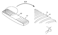
〔実施形態2〕
図13に従来のプラスチックフレネルレンズ81が示されている。このプラスチックフレネルレンズ81の場合は、微細パターン(フルネルパターン)の先端部75の先端eがエッジになっていてその角度αが45度以下である場合があり、この部分が薄肉になっていることがある。このため、実施形態1のプラスチック回折レンズと同様に金型から離型する際に、その微小パターンの先端部75の先端eの離型抵抗が大きく、当該先端eが変形する現象(プラスチック材料がめくれ上がる現象)が生じることがある。
また、上記角度αが45度以下であるときその先端部75の先端eは剛性が小さく、このため、プラスチックフレネルレンズ81の光学面の微細パターンの先端部75の形状精度の低下が見られる。
実施形態2は上記のようなプラスチックフレネルレンズにこの発明を適用した実施形態である。
[Embodiment 2]
FIG. 13 shows a conventional
When the angle α is 45 degrees or less, the tip e of the
The second embodiment is an embodiment in which the present invention is applied to the plastic Fresnel lens as described above.
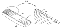
〔実施形態2の実施例1〕
実施形態2の実施例1を図14に示している。この実施例1では、フレネル光学面82に形成された微細パターンと光学素子側面83とが交差して形成される微細パターンの先端部75の先端が光学素子側面83に直角な平面84になっている。
[Example 1 of Embodiment 2]
Example 1 of
なお、図14の実施例1については微細パターンの角度αが45度以下の先端部75についてこの発明の手段を講じればよいのであるが、この実施例1では微細パターンの全ての先端部75にこの発明の手段を講じて形状のバランスが図られており、その先端が光学素子側面83に垂直な平面84になっている。
この実施例1では微細パターンの先端部75の先端は上記平面84になっているので薄肉の部分はないから、成形品を射出成形金型から離型する際の上記先端部75の先端の離型抵抗は大きくなく、また、同先端の剛性は低くない。したがって、上記先端部75の先端が変形(プラスチック材料がめくれ上がる現象)することはなく、先端部75の形状精度が高いプラスチックフレネルレンズが製造される。
In the first embodiment shown in FIG. 14, the means of the present invention may be applied to the
In the first embodiment, since the tip of the
また、微細パターンの先端部75の先端が金型から離型されずに金型内面に付着してしまうことはないので、金型を分解してプラスチック材料を除去し洗浄する必要はない。したがって、金型メンテナンスの回数は少なく、メンテナンスコストは低い。
この実施例1の利点は金型の製作が容易であることである。
In addition, since the tip of the
The advantage of the first embodiment is that the mold can be easily manufactured.
〔実施形態2の実施例2〕
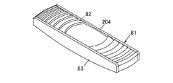
実施形態2の実施例2を図15に示している。この実施例2では光学面に形成された微細パターンと光学素子側面とが交差して形成される微細パターンの先端部75が微細パターンから上方に突出したリブ204と一体になっている。
図15のプラスチックフレネルレンズは、微細パターンの先端部75の全てが上記リブ204と一体になっているので、射出成形金型から離型する際の微細パターンの先端部75の先端の離型抵抗は大きくなく、微細パターンの先端部の先端が変形(プラスチック材料がめくれ上がる現象)することはない。したがって、上記微細パターンの先端部75の形状誤差は大きくなく、形状精度が高いプラスチックフレネルレンズが製造される。また、金型メンテナンスの回数は少なく、メンテナンスコストは低い。
この実施例2の利点は、金型の微細パターン端部角の経時的劣化を抑え長寿命で高安定な成形が実施できることである。
[Example 2 of Embodiment 2]
Example 2 of
In the plastic Fresnel lens shown in FIG. 15, since all of the
The advantage of the second embodiment is that long-life and highly stable molding can be performed while suppressing deterioration of the corner angle of the fine pattern of the mold over time.
〔実施形態3〕
この実施形態3は反射防止機能付きプラスチックレンズ91にこの発明を適用した実施形態である。
従来の反射防止機能付きプラスチックレンズ91が図16に示されている。この従来の反射防止機能付きプラスチックレンズは、一方の光学面が反射防止機能光学面92になっていて、その微細パターンは、透過する光束の波長より短い周期をもつ微細パターンである。
反射防止機能付きプラスチックレンズの場合は、上記微細パターンの先端部75の先端がエッジになっていてその角度が45度以下である場合があり、この部分は薄肉になっていることである。このため、実施形態1のプラスチック回折レンズ、実施形態2のプラスチックフレネルレンズと同様に、射出成形法によってこれを製造すると、冷却時に上記先端部の先端の薄肉の部分が高密度化する。そしてこの高密度化した部分の離型抵抗が大きく、当該部分で変形(プラスチック材料がめくれ上がる現象)が生じる。また、先端の薄肉の部分は剛性が低い。したがって、上記微細パターンの先端部75の先端の形状誤差が大きく、このためその形状精度が低いことがある。
[Embodiment 3]
The third embodiment is an embodiment in which the present invention is applied to a
A
In the case of a plastic lens with an antireflection function, the tip of the
〔実施形態3の実施例1〕
実施形態3の実施例1を図17に示している。この実施例1では、反射防止機能光学面92に形成された微細パターンと光学素子側面93とが交差して形成される先端部75が微細パターンから上方に突出したリブ304と一体になっている。
[Example 1 of Embodiment 3]
Example 1 of
図17の反射防止機能付きプラスチックレンズでは、その微細パターンの先端部75が上記リブ304と一体になっているから、上記リブ304によって微細パターンの先端の冷却速度が緩和されるので、上記微細パターンの先端部の先端の離型抵抗は大きくなく、また、上記先端部75の先端が上記リブで補強されるのでその剛性は低くなく、同先端が変形することはない。したがって、反射防止機能付きプラスチックレンズの反射防止光学面の微細パターン部の先端部75の先端の形状誤差は大きくなく、形状精度が高い反射防止機能付きプラスチックレンズが製造される。また、金型メンテナンスの回数は少なく、メンテナンスコストは低い。
この実施例1の利点は金型の製作が容易であることである。
In the plastic lens with an antireflection function in FIG. 17, since the
The advantage of the first embodiment is that the mold can be easily manufactured.
なお、この反射防止機能付きプラスチックレンズは、その側面93に2〜5度の抜き勾配がつけられており、これにより、型抜きの抵抗が小さくて成形品の取り出しが容易である(因みに、抜き勾配が1度以下では効果が小さく、10度以上では 組み付け時の接着面として扱いにくいから、上記範囲が最適である)ので、型抜き抵抗による光学面の歪みが低減される。したがって、光学面の形状精度が高い反射防止機能付きプラスチックレンズが製造される。
In addition, the plastic lens with an antireflection function has a draft angle of 2 to 5 degrees on the
71:プラスチック回折レンズ
72:回折光学面
73,83,93:光学素子側面
74:光学素子側面に垂直な平面
75:微細パターンの先端部
81:プラスチックフレネルレンズ
82:フレネル光学面
91:反射防止機能付きプラスチックレンズ
92:反射防止機能光学面
94:光学面の長さ方向に凸状に屈曲した円弧面
104:光学素子の厚さ方向に凸状に屈曲した円弧面
114:微細パターンから上方(図面において上方)に凸出したリブ
124:レンズ厚さ方向に傾斜した傾斜面124
204,304:リブ
e:先端(又はエッジ)
71: Plastic diffractive lens 72: Diffractive
204, 304: Rib e: Tip (or edge)
Claims (10)
上記微細パターンの全ての先端部の角度が45度以上であることを特徴とするプラスチック光学素子。 A plastic optical element in which a fine pattern is formed on one optical surface, where the fine pattern intersects the side of the optical element adjacent to the optical surface in a region where the light flux at the end of the optical surface is not transmitted or reflected. In the plastic optical element in which the tip of the pattern is formed,
A plastic optical element characterized in that the angles of all the tips of the fine pattern are 45 degrees or more.
微細パターンの先端部が、微細パターンから上方に突出したリブと一体であることを特徴とする、プラスチック光学素子。 A plastic optical element in which a fine pattern is formed on one optical surface, where the fine pattern intersects the side of the optical element adjacent to the optical surface in a region where the light flux at the end of the optical surface is not transmitted or reflected. In the plastic optical element in which the tip of the pattern is formed,
A plastic optical element characterized in that the tip of the fine pattern is integral with a rib protruding upward from the fine pattern.
Priority Applications (1)
| Application Number | Priority Date | Filing Date | Title |
|---|---|---|---|
| JP2008239768A JP5333986B2 (en) | 2008-09-18 | 2008-09-18 | Plastic optical element having fine pattern on optical surface |
Applications Claiming Priority (1)
| Application Number | Priority Date | Filing Date | Title |
|---|---|---|---|
| JP2008239768A JP5333986B2 (en) | 2008-09-18 | 2008-09-18 | Plastic optical element having fine pattern on optical surface |
Publications (2)
| Publication Number | Publication Date |
|---|---|
| JP2010072350A true JP2010072350A (en) | 2010-04-02 |
| JP5333986B2 JP5333986B2 (en) | 2013-11-06 |
Family
ID=42204181
Family Applications (1)
| Application Number | Title | Priority Date | Filing Date |
|---|---|---|---|
| JP2008239768A Active JP5333986B2 (en) | 2008-09-18 | 2008-09-18 | Plastic optical element having fine pattern on optical surface |
Country Status (1)
| Country | Link |
|---|---|
| JP (1) | JP5333986B2 (en) |
Cited By (3)
| Publication number | Priority date | Publication date | Assignee | Title |
|---|---|---|---|---|
| JP2013020168A (en) * | 2011-07-13 | 2013-01-31 | Ricoh Co Ltd | Optical lens, optical scanner, and image forming apparatus |
| JP2019095469A (en) * | 2017-11-17 | 2019-06-20 | 株式会社東芝 | Semiconductor device and method for manufacturing the same |
| JP2019216242A (en) * | 2017-11-17 | 2019-12-19 | 株式会社東芝 | Semiconductor device |
Families Citing this family (1)
| Publication number | Priority date | Publication date | Assignee | Title |
|---|---|---|---|---|
| CN106556884A (en) * | 2015-09-25 | 2017-04-05 | 高准精密工业股份有限公司 | Optical lens |
Citations (11)
| Publication number | Priority date | Publication date | Assignee | Title |
|---|---|---|---|---|
| JPH07206475A (en) * | 1993-12-29 | 1995-08-08 | Toyota Motor Corp | Water repellent layer carrying member |
| JP2002221604A (en) * | 2001-01-25 | 2002-08-09 | Sony Corp | Optical element and optical pickup device |
| JP2003047833A (en) * | 2001-08-07 | 2003-02-18 | Reika Kogyo Kk | Vibromixer |
| WO2003047833A1 (en) * | 2001-12-04 | 2003-06-12 | Riken | Method and device for manufacturing large curved double-sided fresnel lens |
| JP2005258392A (en) * | 2004-02-12 | 2005-09-22 | Ricoh Co Ltd | Optical scanner and image forming apparatus |
| WO2006009193A1 (en) * | 2004-07-23 | 2006-01-26 | Kuraray Co., Ltd. | Back projection-type screen and back projection-type projection device |
| JP2007134316A (en) * | 2005-10-14 | 2007-05-31 | Toshiba Corp | Lighting apparatus |
| JP2007148017A (en) * | 2005-11-28 | 2007-06-14 | Dainippon Printing Co Ltd | Fresnel lens sheet, transmission screen, and rear projection type display device |
| WO2008142846A1 (en) * | 2007-05-18 | 2008-11-27 | Panasonic Corporation | Three-dimensional image display device |
| JP2009015102A (en) * | 2007-07-06 | 2009-01-22 | Citizen Finetech Miyota Co Ltd | Light coupling body and image display apparatus |
| JP2009223093A (en) * | 2008-03-18 | 2009-10-01 | Ricoh Co Ltd | Diffraction optical element and method |
-
2008
- 2008-09-18 JP JP2008239768A patent/JP5333986B2/en active Active
Patent Citations (11)
| Publication number | Priority date | Publication date | Assignee | Title |
|---|---|---|---|---|
| JPH07206475A (en) * | 1993-12-29 | 1995-08-08 | Toyota Motor Corp | Water repellent layer carrying member |
| JP2002221604A (en) * | 2001-01-25 | 2002-08-09 | Sony Corp | Optical element and optical pickup device |
| JP2003047833A (en) * | 2001-08-07 | 2003-02-18 | Reika Kogyo Kk | Vibromixer |
| WO2003047833A1 (en) * | 2001-12-04 | 2003-06-12 | Riken | Method and device for manufacturing large curved double-sided fresnel lens |
| JP2005258392A (en) * | 2004-02-12 | 2005-09-22 | Ricoh Co Ltd | Optical scanner and image forming apparatus |
| WO2006009193A1 (en) * | 2004-07-23 | 2006-01-26 | Kuraray Co., Ltd. | Back projection-type screen and back projection-type projection device |
| JP2007134316A (en) * | 2005-10-14 | 2007-05-31 | Toshiba Corp | Lighting apparatus |
| JP2007148017A (en) * | 2005-11-28 | 2007-06-14 | Dainippon Printing Co Ltd | Fresnel lens sheet, transmission screen, and rear projection type display device |
| WO2008142846A1 (en) * | 2007-05-18 | 2008-11-27 | Panasonic Corporation | Three-dimensional image display device |
| JP2009015102A (en) * | 2007-07-06 | 2009-01-22 | Citizen Finetech Miyota Co Ltd | Light coupling body and image display apparatus |
| JP2009223093A (en) * | 2008-03-18 | 2009-10-01 | Ricoh Co Ltd | Diffraction optical element and method |
Cited By (4)
| Publication number | Priority date | Publication date | Assignee | Title |
|---|---|---|---|---|
| JP2013020168A (en) * | 2011-07-13 | 2013-01-31 | Ricoh Co Ltd | Optical lens, optical scanner, and image forming apparatus |
| JP2019095469A (en) * | 2017-11-17 | 2019-06-20 | 株式会社東芝 | Semiconductor device and method for manufacturing the same |
| US10396060B2 (en) | 2017-11-17 | 2019-08-27 | Kabushiki Kaisha Toshiba | Semiconductor device and method for manufacturing same |
| JP2019216242A (en) * | 2017-11-17 | 2019-12-19 | 株式会社東芝 | Semiconductor device |
Also Published As
| Publication number | Publication date |
|---|---|
| JP5333986B2 (en) | 2013-11-06 |
Similar Documents
| Publication | Publication Date | Title |
|---|---|---|
| US7525710B2 (en) | Scanning and imaging optical system, optical scanner, and image forming apparatus with lenses of different signs and refractive index distribution increasing toward rim | |
| US7565078B2 (en) | Thread structure for an optical lens | |
| JP5333986B2 (en) | Plastic optical element having fine pattern on optical surface | |
| WO2018105577A1 (en) | Lens unit and imaging device | |
| JP2005004208A (en) | Ftheta LENS FOR OPTICAL SCANNING DEVICE, AND OPTICAL SCANNING DEVICE | |
| JP5840936B2 (en) | Vehicular lamp and manufacturing method thereof | |
| WO2005119358A1 (en) | Fresnel lens sheet, rear projection tyep screen and rear projection type image display unit | |
| JP2007178793A (en) | Polarization retardation plate | |
| JP5555816B2 (en) | OPTICAL ELEMENT, IMAGING DEVICE EQUIPPED WITH THE SAME, AND OPTICAL ELEMENT MANUFACTURING METHOD | |
| JP5031485B2 (en) | Plastic lens, optical scanning device, and image forming apparatus | |
| JP5555817B2 (en) | OPTICAL ELEMENT, IMAGING DEVICE EQUIPPED WITH THE SAME, AND OPTICAL ELEMENT MANUFACTURING METHOD | |
| JP4899964B2 (en) | Optical lens and lens manufacturing method | |
| JP4751184B2 (en) | Plastic optical element, optical scanning device, and image forming apparatus equipped with the optical scanning device | |
| JP5315484B1 (en) | OPTICAL ELEMENT, IMAGING DEVICE EQUIPPED WITH THE SAME, AND OPTICAL ELEMENT MANUFACTURING METHOD | |
| JP2007206490A (en) | Composite type optical element and optical system | |
| JP2012189995A (en) | Diffraction optical element and imaging apparatus using the same | |
| JP6636421B2 (en) | Free-form surface lens, free-form surface lens design method, and projection-type image display device | |
| JP6957133B2 (en) | Glass molding lens, lens molding equipment and lens manufacturing method | |
| JP2009244529A (en) | Light shielding part and lens barrel | |
| WO2012114408A1 (en) | Diffraction optical element and imaging device provided with same | |
| JP5086852B2 (en) | Diffractive optical element and method | |
| US8418516B2 (en) | Manufacturing method for optical element | |
| JP5247235B2 (en) | Optical element and method of manufacturing the optical element | |
| JP2016004098A (en) | Optical element and imaging apparatus including the same | |
| JP6079186B2 (en) | Scanning lens |
Legal Events
| Date | Code | Title | Description |
|---|---|---|---|
| A621 | Written request for application examination |
Free format text: JAPANESE INTERMEDIATE CODE: A621 Effective date: 20110701 |
|
| A131 | Notification of reasons for refusal |
Free format text: JAPANESE INTERMEDIATE CODE: A131 Effective date: 20130305 |
|
| A521 | Written amendment |
Free format text: JAPANESE INTERMEDIATE CODE: A523 Effective date: 20130501 |
|
| A131 | Notification of reasons for refusal |
Free format text: JAPANESE INTERMEDIATE CODE: A131 Effective date: 20130618 |
|
| A521 | Written amendment |
Free format text: JAPANESE INTERMEDIATE CODE: A523 Effective date: 20130619 |
|
| TRDD | Decision of grant or rejection written | ||
| A01 | Written decision to grant a patent or to grant a registration (utility model) |
Free format text: JAPANESE INTERMEDIATE CODE: A01 Effective date: 20130708 |
|
| R151 | Written notification of patent or utility model registration |
Ref document number: 5333986 Country of ref document: JP Free format text: JAPANESE INTERMEDIATE CODE: R151 |
|
| A61 | First payment of annual fees (during grant procedure) |
Free format text: JAPANESE INTERMEDIATE CODE: A61 Effective date: 20130721 |