JP2010056520A - Optical filter and method of manufacturing the same - Google Patents
Optical filter and method of manufacturing the same Download PDFInfo
- Publication number
- JP2010056520A JP2010056520A JP2009098294A JP2009098294A JP2010056520A JP 2010056520 A JP2010056520 A JP 2010056520A JP 2009098294 A JP2009098294 A JP 2009098294A JP 2009098294 A JP2009098294 A JP 2009098294A JP 2010056520 A JP2010056520 A JP 2010056520A
- Authority
- JP
- Japan
- Prior art keywords
- layer
- aluminum
- metal pattern
- pattern layer
- antireflection
- Prior art date
- Legal status (The legal status is an assumption and is not a legal conclusion. Google has not performed a legal analysis and makes no representation as to the accuracy of the status listed.)
- Granted
Links
Images

Landscapes
- Shielding Devices Or Components To Electric Or Magnetic Fields (AREA)
- Devices For Indicating Variable Information By Combining Individual Elements (AREA)
- Surface Treatment Of Optical Elements (AREA)
- Laminated Bodies (AREA)
Abstract
Description
本発明は各種の用途の光学フィルタ、中でも特に画像表示装置(ディスプレイ)の前面に配置するのに好適な、電磁波遮蔽性と光鏡面反射防止性とを有するフィルタと、その製造方法に関する。 The present invention relates to an optical filter for various uses, and particularly to a filter having electromagnetic wave shielding properties and optical specular reflection prevention properties, which is suitable for being placed on the front surface of an image display device (display), and a method for producing the same.
現在、電磁波遮蔽フィルタは、ディスプレイの前面に配置する用途などで使用されており、そのなかでも代表的にはプラズマディスプレイ(PDPともいう)用途がある。プラズマディスプレイ用の電磁波遮蔽フィルタにおいて、電磁波遮蔽性能と光透過性とを両立させた金属パターンとしてはメッシュ状のパターンが多く用いられている。金属パターン(EMIメッシュ)は、透明基材に金属箔を透明接着剤で貼り合せた後、フォトリソグラフィー法により金属箔をメッシュ状にケミカルエッチングして作ることができる(特許文献1、特許文献2)。
Currently, electromagnetic wave shielding filters are used for applications such as disposing on the front surface of a display, and among them, there are typically plasma display (also referred to as PDP) applications. In an electromagnetic wave shielding filter for a plasma display, a mesh pattern is often used as a metal pattern that achieves both electromagnetic wave shielding performance and light transmittance. A metal pattern (EMI mesh) can be formed by bonding a metal foil to a transparent substrate with a transparent adhesive and then chemically etching the metal foil into a mesh shape by a photolithography method (
金属箔の金属の材質としては、特許文献などでは特に限定しない文献が多い(特許文献1、特許文献2)。例示される金属としては銅の他、アルミニウム(特許文献2)等の高電導率のものが挙げられている。しかし、事実上、市場に流通している電磁波遮蔽フィルタのEMIメッシュは、銅、具体的には銅箔しか用いられておらず、アルミニウム箔を用いたものはなく実用化されていない。
なお、本発明において単に電磁波という場合は、周波数が上記範囲を中心とするKHz〜GHz帯近辺の電磁波のことをいう。赤外線、可視光線、紫外線、X線等は含まないものとする(例えば、赤外線帯域の周波数の電磁波は赤外線と呼称する)。
As a metal material of the metal foil, there are many documents that are not particularly limited in Patent Documents (
In the present invention, the term “electromagnetic wave” means an electromagnetic wave in the vicinity of the KHz to GHz band whose frequency is centered on the above range. It does not include infrared rays, visible rays, ultraviolet rays, X-rays, etc. (for example, electromagnetic waves having a frequency in the infrared band are referred to as infrared rays).
また、ディスプレイ用フィルタには、電磁波遮蔽性とともに、外来光反射防止等の光学フィルタ機能が求められるが、金属パターンを形成した透明基材に反射防止剤を塗布すると、金属パターン層と透明基材との凹凸により、反射防止剤の塗りムラや気泡の混入が起こり、反射防止効果が不十分なものとなる。この問題を解決するために、金属パターン層と透明基材との凹凸を平坦化するための透明な平坦化層を塗工により設け、その上面に平坦化層よりも屈折率の低い反射防止層を塗工又はシート積層により設けることが提案されている(特許文献3)。 In addition, the display filter is required to have an electromagnetic wave shielding property and an optical filter function such as antireflection of extraneous light. When an antireflection agent is applied to a transparent substrate on which a metal pattern is formed, the metal pattern layer and the transparent substrate are used. As a result, uneven coating of the antireflective agent and mixing of bubbles occur, and the antireflection effect becomes insufficient. In order to solve this problem, a transparent flattening layer for flattening the unevenness between the metal pattern layer and the transparent substrate is provided by coating, and an antireflection layer having a lower refractive index than the flattening layer is provided on the upper surface. It has been proposed to provide the film by coating or sheet lamination (Patent Document 3).
近年、画像表示装置(ディスプレイ)の普及促進において、高価な電磁波遮蔽フィルタはその妨げとなっており、電磁波遮蔽フィルタの低コスト化の為には、銅箔よりも安価なアルミニウム箔の採用が考えられる。
そこで、我々は、低コスト化を狙い、金属パターン(EMIメッシュ)の金属材料として、銅箔よりも安いアルミニウム箔を用いた電磁波遮蔽フィルタの検討を行ったが、その結果、アルミニウム箔の実用化には、次の解決すべき課題があることがわかった。なお、以下の課題は、パターンの線幅及び厚みの寸法が100μm程度以上の場合は目立たない。高品質のディスプレイ用途の為に透視性を追及すべく、パターンの線幅及び厚みの寸法が10〜20μm程度以下に微細化した場合において、特に顕在化してくるものであることも判明した。
In recent years, the promotion of the spread of image display devices (displays) has been hampered by expensive electromagnetic shielding filters, and in order to reduce the cost of electromagnetic shielding filters, the use of aluminum foil that is less expensive than copper foil is considered. It is done.
Therefore, we studied electromagnetic wave shielding filters using aluminum foil cheaper than copper foil as the metal material of the metal pattern (EMI mesh) with the aim of lowering the cost. Has the following problems to be solved. The following problems are not noticeable when the line width and thickness of the pattern are about 100 μm or more. It has also been found that the line width and thickness of the pattern are particularly manifested when the line width and thickness are reduced to about 10 to 20 μm or less in order to pursue transparency for high-quality display applications.
(a)アルミニウム自体が活性が高く、表面にアルミニウムの酸化皮膜が存在し、これが耐腐食膜となってケミカルエッチングを阻害する。
(b)エッチング液に接触した領域の酸化皮膜が一部除去されると、アルミニウム自体は化学的に活性の為、除去された部分がまだ除去されていない部分に対して急速にエッチングが進んでしまい、均一な安定したエッチングが困難である。
(c)上記(a)及び(b)の結果として、金属パターンのライン部の輪郭に、ギザ(zigzag状のこと。ラインの輪郭に凹凸があって直線性が悪くギザギザしている形態をこのように呼称する。)や断線が発生し、ラインのパターン精度が、銅箔の場合に比べてアルミニウムは劣る。
(A) Aluminum itself has high activity, and an aluminum oxide film is present on the surface, which becomes a corrosion-resistant film and inhibits chemical etching.
(B) When a portion of the oxide film in the region in contact with the etching solution is removed, the aluminum itself is chemically active, so that the removed portion is rapidly etched against the portion that has not yet been removed. Therefore, uniform and stable etching is difficult.
(C) As a result of the above (a) and (b), the contour of the line portion of the metal pattern has a zigzag shape. In other words, aluminum is inferior in the pattern accuracy of the line compared to the case of copper foil.
以上の結果、銅箔と比べて画像表示装置で要求される微細なパターン(例えばライン幅10〜20μm、パターンの厚み10〜20μm程度)が得られない。そして、ギザは光透過性を実現する開口部の面積率のムラとなって表示画面の面ムラに繋がり、断線は電磁波遮蔽性能の低下に繋がる。
また、反射防止剤の塗りムラや気泡の混入を防止する為に平坦化層を1層追加することは、加工費用の高騰、加工時間と工程数増による生産効率の低下に繋がる。
As a result, a fine pattern (for example, a line width of 10 to 20 μm and a pattern thickness of about 10 to 20 μm) required by the image display device cannot be obtained as compared with the copper foil. Then, the unevenness leads to unevenness in the area ratio of the opening that realizes light transmittance, leading to unevenness in the surface of the display screen, and disconnection leads to deterioration in electromagnetic wave shielding performance.
Further, adding one flattening layer in order to prevent uneven coating of the antireflective agent and mixing of bubbles leads to a rise in processing cost and a decrease in production efficiency due to an increase in processing time and the number of processes.
すなわち、本発明の目的は、金属パターンの材質を銅から安価なアルミニウムに代えると生じる、ケミカルエッチングで形成したアルミニウムパターンのパターン精度不良を解消して、アルミニウムを用いた安価でしかも実用可能な電磁波遮蔽フィルタであって、かつ、優れた光鏡面反射防止性を有する光学フィルタを提供することである。
また、これに加えて更に、塗りムラや気泡の混入のない優れた光鏡面反射防止性を有する光学フィルタを提供することである。
また、そのような光学フィルタの製造方法を、加工費用の高騰、加工時間と工程数増による生産効率の低下なしに光学フィルタを製造する方法を提供することである。
That is, the object of the present invention is to eliminate the poor pattern accuracy of an aluminum pattern formed by chemical etching, which occurs when the material of the metal pattern is changed from copper to inexpensive aluminum, and to provide an inexpensive and practical electromagnetic wave using aluminum. An object of the present invention is to provide an optical filter that is a shielding filter and has excellent optical specular reflection prevention.
In addition to this, it is an object to provide an optical filter having excellent optical mirror surface antireflection properties without coating unevenness and mixing of bubbles.
Another object of the present invention is to provide a method for manufacturing an optical filter without increasing the processing cost and reducing the production efficiency due to the increase in processing time and the number of processes.
そこで、本発明は、透明基材上に、金属パターン層と、透明樹脂からなり該金属パターン層の凹凸を埋めてその表面を平坦面としてなる平坦化層と、光鏡面反射防止層がこの順に積層されてなるフィルタであって、該金属パターン層がアルミニウムパターン層であり、アルミニウムパターン層の少なくとも上面(透明基材に対して遠い側のアルミニウム層表面)のアルミニウムの酸化皮膜の厚みが0〜13Åであるフィルタおよびその製造方法を提供する。 Therefore, the present invention provides a metal pattern layer, a flattening layer made of a transparent resin, filling the unevenness of the metal pattern layer to make the surface flat, and an optical specular antireflection layer in this order on a transparent substrate. The filter is a laminated filter, wherein the metal pattern layer is an aluminum pattern layer, and the thickness of the aluminum oxide film on at least the upper surface of the aluminum pattern layer (the surface of the aluminum layer far from the transparent substrate) is 0 to Provided is a filter that is 13 mm and a method for manufacturing the same.
このように、少なくとも上面側のアルミニウムの酸化皮膜の厚みを薄く規定することで、アルミニウムパターンをケミカルエッチングで形成する際に安定したエッチングが可能でエッチング品質が改善する為に、ライン輪郭部のギザや断線となる不良が解消してパターン精度が向上し、ひいては、電磁波遮蔽性(表面抵抗値)のバラツキやヘーズ(曇価)の上昇を避けられる。この結果、銅よりも安価なアルミニウムを利用して、材料的に安価な電磁波遮蔽フィルタを実用化できる。 In this way, by defining the thickness of at least the aluminum oxide film on the upper surface side to be thin, stable etching is possible when the aluminum pattern is formed by chemical etching, and the etching quality is improved. In addition, the defect that causes disconnection is eliminated, the pattern accuracy is improved, and as a result, variations in electromagnetic shielding properties (surface resistance value) and haze (cloudiness value) can be avoided. As a result, an electromagnetic wave shielding filter that is inexpensive in terms of material can be put into practical use by using aluminum that is less expensive than copper.
本発明のフィルタによれば、金属パターンに銅よりも安価なアルミニウムを用いても、ケミカルエッチング形成時のライン輪郭のギザ(zigzag)や断線が解消してパターン精度が向上し、電磁波遮蔽性(表面抵抗値)のバラツキ、ヘーズの上昇を避けられ、安価な電磁波遮蔽フィルタを実用化できる。
しかも、製造面でも、アルミニウムの酸化皮膜はそのままでケミカルエッチングできるので、酸化皮膜の追加的な除去工程が不要で、製造工程の複雑化やコストアップも避けられる。
また、本発明のフィルタは、金属パターン層の凹凸を埋めてその表面が平坦面である平坦化層と、光鏡面反射防止層を設けたことにより、電磁波遮蔽性とともに、優れた光鏡面反射防止性とを有する、特にディスプレイ用に好適な、光学フィルタとなる。
According to the filter of the present invention, even when aluminum which is cheaper than copper is used for the metal pattern, the line contour zigzag and disconnection at the time of chemical etching formation are eliminated, the pattern accuracy is improved, and electromagnetic wave shielding ( Variations in the surface resistance) and haze increase can be avoided, and an inexpensive electromagnetic wave shielding filter can be put into practical use.
Moreover, since the aluminum oxide film can be chemically etched as it is in terms of production, an additional removal process of the oxide film is unnecessary, and the manufacturing process is not complicated and the cost is increased.
In addition, the filter of the present invention is provided with a flattened layer whose surface is flat by filling the unevenness of the metal pattern layer, and an optical specular antireflection layer, thereby providing excellent optical specular antireflection as well as electromagnetic shielding properties. Therefore, the optical filter is suitable for a display.
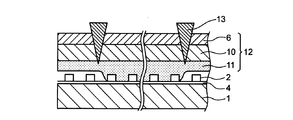
図1は、本発明による光学フィルタの一形態の層構成を示す断面の概念図である。
同図の場合、透明基材1の一方の面に、アルミニウムパターン2が形成され、アルミニウムパターン2はその上面(透明基材1から遠い側の表面)及び下面(透明基材1に近い側の表面)の表面にはアルミニウムの酸化皮膜3を有し、少なくとも上面の酸化皮膜の厚みが0〜13Åの範囲となっている。そして、同図の形態例では、このアルミニウムパターン2は、その下面側の酸化皮膜3の表面で透明接着剤層4によって透明基材1に接着固定され積層されている。透明接着剤層4はアルミニウムパターンの開口部も含めて透明基材1の全面に形成されている。
そして、本発明による光学フィルタは、表面に酸化皮膜3を有するアルミニウムパターン2の上に、透明樹脂からなり該アルミニウムパターンの凹凸を埋めてその表面が平坦面である平坦化層5と、光鏡面反射防止層6がこの順に積層されている。なお、図1において、上方が観察者(視聴者)側であり、下方が画像表示装置側である。
以下、本発明の光学フィルタの構成につき、詳細に説明する。
FIG. 1 is a conceptual cross-sectional view showing a layer configuration of one form of an optical filter according to the present invention.
In the case of the figure, an
The optical filter according to the present invention comprises a flattening layer 5 made of a transparent resin and having a flat surface on the surface of the
Hereinafter, the configuration of the optical filter of the present invention will be described in detail.
[透明基材]
透明基材1は、可視領域での透明性(光透過性)、耐熱性、機械的強度等の要求物性を考慮して、公知の材料及び厚みを適宜選択すればよく、ガラス、セラミックス等の透明無機物の板、或いは樹脂板など板状体の剛直物でもよい。ただし、生産性に優れるロール・トゥ・ロールでの連続加工適性を考慮すると、フレキシブルな樹脂フィルム(乃至シート)が好ましい。なお、ロール・トゥ・ロールとは、巻取(ロール)から巻き出して供給し、適宜加工を施し、その後、巻取に巻き取って保管する加工方式をいう。
[Transparent substrate]
The
樹脂フィルム、樹脂板の樹脂としては、例えば、ポリエチレンテレフタレート、ポリエチレンナフタレート、エチレングリコール−1,4シクロヘキサンジメタノール−テレフタール酸共重合体、エチレングリコール−テレフタール酸−イソフタール酸共重合体などのポリエステル系樹脂、ポリメチルメタクリレートなどのアクリル系樹脂、ポリプロピレン、シクロオレフィン重合体などのポリオレフィン系樹脂、トリアセチルセルロースなどのセルロース系樹脂、ポリカーボネート系樹脂、ポリイミド系樹脂等である。なかでも、ポリエチレンテレフタレートはその2軸延伸フィルムが耐熱性、機械的強度、光透過性、コスト等の点で好ましい透明基材である。
透明無機物としては、ソーダ硝子、カリ硝子、硼珪酸硝子、鉛硝子等の硝子、或いはPLZT、石英等の透明セラミックス等である。
Examples of resins for resin films and resin plates include polyesters such as polyethylene terephthalate, polyethylene naphthalate, ethylene glycol-1,4 cyclohexanedimethanol-terephthalic acid copolymer, and ethylene glycol-terephthalic acid-isophthalic acid copolymer. Examples thereof include resins, acrylic resins such as polymethyl methacrylate, polyolefin resins such as polypropylene and cycloolefin polymers, cellulose resins such as triacetyl cellulose, polycarbonate resins, and polyimide resins. Among them, polyethylene terephthalate is a transparent base material whose biaxially stretched film is preferable in terms of heat resistance, mechanical strength, light transmittance, cost, and the like.
Examples of the transparent inorganic material include soda glass, potash glass, borosilicate glass, lead glass, and other transparent ceramics such as PLZT and quartz.
透明基材の厚みは基本的には特に制限はなく用途等に応じ適宜選択し、フレキシブルな樹脂フィルムを利用する場合、例えば12〜500μm、好ましくは25〜200μm程度である。樹脂や透明無機物の板を利用する場合、例えば、500〜5000μm程度である。 The thickness of the transparent substrate is basically not particularly limited and is appropriately selected depending on the application. When a flexible resin film is used, it is, for example, about 12 to 500 μm, preferably about 25 to 200 μm. In the case of using a resin or transparent inorganic plate, the thickness is, for example, about 500 to 5000 μm.
なお、透明基材の樹脂中には、必要に応じて適宜、紫外線吸収剤、着色剤、充填剤、可塑剤、帯電防止剤などの公知の添加剤を添加できる。
また、透明基材は、その表面に、コロナ放電処理、プライマー処理、下地処理などの公知の易接着処理を行ったものでもよい。
In addition, known additives such as an ultraviolet absorber, a colorant, a filler, a plasticizer, and an antistatic agent can be appropriately added to the resin of the transparent substrate as necessary.
The transparent base material may be obtained by performing known easy adhesion treatment such as corona discharge treatment, primer treatment, and ground treatment on the surface.
[アルミニウムパターン]
アルミニウムパターン2はアルミニウムで形成したパターン層であり、該層自体は不透明であるが、開口部など該層の非形成部を設けたパターンとすることによって、電磁波遮蔽性能と光透過性とを両立させた層である。そして、本発明のアルミニウムパターン2は少なくともその上面に特定の厚み範囲0〜13Åのアルミニウムの酸化皮膜3を有する。なお、1Å=0.1nmである。
[Aluminum pattern]
The
アルミニウムパターンのアルミニウムは、アルミニウムを主成分とし、アルミニウム純金属の他にアルミニウム合金でもよくこれらを纏めて本発明ではアルミニウムというが、アルミニウムの純度が低いと導電性が低下するので、純度は電磁波遮蔽性能の点では高い方が好ましく、純度が99.0%以上のアルミニウムが好ましい。このような純度が99.0%以上のアルミニウムを利用したアルミニウムパターンは、JIS H4160(アルミニウム及びアルミニウム合金はく)、JIS H4170(高純度アルミニウムはく)で規定されるアルミニウム箔に準じた箔を利用することで形成できる。 Aluminum in the aluminum pattern is mainly composed of aluminum, and may be aluminum alloy in addition to aluminum pure metal. These are collectively referred to as aluminum in the present invention. However, since the conductivity decreases when the purity of aluminum is low, the purity is shielded against electromagnetic waves. Higher is preferable in terms of performance, and aluminum having a purity of 99.0% or more is preferable. The aluminum pattern using aluminum having a purity of 99.0% or more is made of a foil conforming to the aluminum foil defined in JIS H4160 (aluminum and aluminum alloy foil) and JIS H4170 (high purity aluminum foil). It can be formed by using it.
なお、アルミニウムパターンはアルミニウム箔から形成するのではなく、透明基材上にアルミニウムを気相成長法、例えば真空蒸着法で形成したアルミニウム蒸着膜から形成したものを利用してもよい。 Note that the aluminum pattern is not formed from an aluminum foil, but an aluminum pattern formed from an aluminum vapor deposition film formed by vapor deposition, for example, a vacuum vapor deposition method, on a transparent substrate may be used.
アルミニウムパターンの厚みは、電磁波遮蔽性能、加工適性、機械的強度などの点から適宜選択すればよく、具体的には1〜100μm、好ましくは5〜20μm、より好ましくは8〜15μmである。厚みが薄いと電磁波遮蔽性能、機械的強度などが低下し、厚みが厚いと加工適性が低下する。 The thickness of the aluminum pattern may be appropriately selected from the viewpoints of electromagnetic wave shielding performance, processability, mechanical strength, and the like, specifically 1 to 100 μm, preferably 5 to 20 μm, more preferably 8 to 15 μm. If the thickness is thin, electromagnetic wave shielding performance, mechanical strength and the like are lowered, and if the thickness is thick, workability is lowered.
アルミニウムパターンの平面視のパターンの形状は、例えばメッシュ形状、ストライプ形状などの電磁波遮蔽性能と光透過性とを両立させた公知のパターンである。なかでもメッシュ形状、それも正方格子形状が代表的であり、この他、格子形状で言えば例えば長方形格子、菱形格子、六角格子、三角格子などがある。メッシュはこれら形状からなる複数の開口部を有し、開口部間は開口部を区画するライン部(線部又は線条部)となる。ライン部は通常、幅均一でライン状のものであり、また通常は開口部及び開口部間は、全て各々同一形状で同一サイズとなる。 The shape of the aluminum pattern in plan view is, for example, a known pattern in which both electromagnetic wave shielding performance and light transmittance such as a mesh shape and a stripe shape are compatible. Among them, a mesh shape and a square lattice shape are typical, and in addition, examples of the lattice shape include a rectangular lattice, a rhombus lattice, a hexagonal lattice, and a triangular lattice. The mesh has a plurality of openings having these shapes, and the openings are line portions (line portions or line portions) that define the openings. The line part is usually a line having a uniform width, and usually the opening part and the opening part are all the same shape and the same size.
なお、上記パターンは、ディスプレイ用途では、電磁波遮蔽フィルタの画像表示に影響しない四辺周辺部には、接地用導通の為に開口部を設けないベタパターンか、あっても占有面積比率が小さい接地領域を、開口部を有する内部の画像表示領域の周囲に有することがある。 In addition, the above pattern is a solid pattern in which an opening is not provided for grounding continuity in the periphery of the four sides that does not affect the image display of the electromagnetic wave shielding filter in a display application, or a grounding area with a small occupied area ratio. May be provided around an internal image display area having an opening.
パターンのライン部のライン幅は例えば5〜50μm、本発明の効果がより際立つ点ではより細い5〜30μmであり、より好ましくは5〜20μmである。ラインの繰り返し周期であるライン間隔(ピッチ)は例えば100〜500μmである。 The line width of the line portion of the pattern is, for example, 5 to 50 μm, and is 5 to 30 μm, more preferably 5 to 20 μm, from the standpoint of the effect of the present invention. The line interval (pitch), which is a line repetition period, is, for example, 100 to 500 μm.
(パターン形成)
アルミニウムパターンのパターンを形成するには、透明基材上にアルミニウム箔などパターン形成前のアルミニウム層を積層した後、ケミカルエッチングによって形成できる。
ケミカルエッチング時のレジストパターンのパターン形成はフォトリソグラフィー法(パターン露光法)、印刷法などの公知のパターン形成法を適宜選択すればよい。なかでも、フォトリソグラフィー法は印刷法に比べて、電磁波遮蔽フィルタに要求されるライン幅やその均一性など高精度のパターンを安定的に形成できる点で好ましい方法である。
(Pattern formation)
In order to form the pattern of the aluminum pattern, it can be formed by chemical etching after laminating an aluminum layer such as an aluminum foil on the transparent base material before pattern formation.
For pattern formation of the resist pattern during chemical etching, a known pattern formation method such as a photolithography method (pattern exposure method) or a printing method may be appropriately selected. Among these, the photolithography method is a preferable method compared to the printing method in that a highly accurate pattern such as a line width required for the electromagnetic wave shielding filter and its uniformity can be stably formed.
アルミニウムパターンをケミカルエッチングする際のエッチング液としては、公知のエッチング液を適宜選択使用すればよい。例えば、塩化第二鉄を含む酸性のエッチング液である。
エッチングは、アルミニウム層の上面のレジストパターン非形成部におけるアルミニウムの酸化皮膜も含めて行われる。エッチングの前処理として、該上面のアルミニウムの酸化皮膜の除去は特に必要ない。
そして、レジストパターン形成部に対応した、上面や下面のアルミニウムの酸化皮膜3は、アルミニウムパターン2の上面や下面の酸化皮膜3となって残る。
A known etching solution may be appropriately selected and used as an etching solution for chemically etching the aluminum pattern. For example, an acidic etching solution containing ferric chloride.
The etching is performed including the aluminum oxide film in the resist pattern non-formation portion on the upper surface of the aluminum layer. It is not particularly necessary to remove the aluminum oxide film on the upper surface as a pretreatment for etching.
Then, the
[アルミニウムの酸化皮膜]
アルミニウムの酸化皮膜はアルミニウム酸化物を含む層であり、アルミニウムパターンをアルミニウム箔を利用して形成する場合、アルミニウムの酸化皮膜は箔の上面及び下面の表裏両面に存在するが、本発明ではケミカルエッチングでパターン形成する際に、はじめにエッチングされる側、つまり上面側について、その厚みを規定する。アルミニウムパターンの少なくとも上面のアルミニウムの酸化皮膜の厚みについて、その上限を13Å、好ましくは12Å、より好ましくは10Å、更に好ましくは8Åとする。
少なくとも上面のアルミニウムの酸化皮膜の厚みについて、その上限を上記のようにすることで、該酸化皮膜がたとえ存在したままでも、安定したケミカルエッチングが可能となり、銅を安価なアルミニウムに変更したが故のパターン精度不良を回避できる。
[Aluminum oxide film]
An aluminum oxide film is a layer containing an aluminum oxide. When an aluminum pattern is formed using an aluminum foil, the aluminum oxide film exists on both the top and bottom surfaces of the foil. When the pattern is formed, the thickness of the first etched side, that is, the upper surface side is defined. The upper limit of the thickness of the aluminum oxide film on at least the upper surface of the aluminum pattern is 13 mm, preferably 12 mm, more preferably 10 mm, and still more preferably 8 mm.
By setting the upper limit of the thickness of the aluminum oxide film on at least the upper surface as described above, stable chemical etching is possible even if the oxide film is still present, and copper is changed to inexpensive aluminum. The pattern accuracy defect can be avoided.
ところで、普通に製造されるアルミニウム箔は圧延法で製造され、アルミニウム塊の圧延工程、焼鈍工程を経る箔製造工程、その後の空気中保管など、常温(20℃、50%RH前後)で製造保管することによって、活性なアルミニウムは表面に不可逆的にアルミニウムの酸化皮膜が形成されるが、本発明のように薄い酸化皮膜とはならずに、より厚みの厚い15Å以上、通常20〜100Å程度の酸化皮膜となる。 By the way, normally manufactured aluminum foil is manufactured by a rolling method, and manufactured and stored at normal temperature (20 ° C., around 50% RH), such as aluminum ingot rolling process, foil manufacturing process through annealing process, and subsequent storage in air. By doing so, an active aluminum irreversibly forms an oxide film of aluminum on the surface, but it does not become a thin oxide film as in the present invention, but is thicker than 15 mm, usually about 20 to 100 mm. It becomes an oxide film.
また、アルミニウムパターン上面のアルミニウムの酸化皮膜の厚みの下限は、ケミカルエッチングを阻害しない観点からは、0(零)Å、つまり酸化皮膜が存在しなくてもよい。
ただ、アルミニウムの酸化皮膜は、不動態膜と言われており、アルミニウム箔を加工、搬送、保管する過程中において、アルミニウム箔の内部に(不用意な、望まれない)酸化乃至は腐食が進行することを防止する機能を有するので、この点では2〜3Å程度の、緻密なアルミニウム不動態膜としての酸化皮膜を形成しておいてもよい。
In addition, the lower limit of the thickness of the aluminum oxide film on the upper surface of the aluminum pattern is 0 (zero), that is, no oxide film may be present from the viewpoint of not inhibiting chemical etching.
However, the aluminum oxide film is said to be a passive film, and during the process of processing, transporting and storing the aluminum foil, oxidation or corrosion progresses (inadvertently or undesirably) inside the aluminum foil. In this respect, an oxide film as a dense aluminum passivating film having a thickness of about 2 to 3 mm may be formed.
なお、上(下)面にアルミニウムの酸化皮膜が存在しないアルミニウムパターンは、真空中、不活性気体中でパターン形成前のアルミニウム層を透明基材上に形成し、酸化皮膜生成前にアルミニウム層の上面を樹脂被覆し酸化反応を遮断するなどすれば可能である。その後、ケミカルエッチングで所定のパターンを形成すれば、上(下)面にアルミニウムの酸化皮膜が存在しないアルミニウムパターンとなる。 In addition, the aluminum pattern in which the aluminum oxide film does not exist on the upper (lower) surface is formed on the transparent substrate in vacuum and in an inert gas on the transparent substrate, and the aluminum layer is formed before the oxide film is formed. This can be achieved by coating the upper surface with a resin to block the oxidation reaction. Thereafter, when a predetermined pattern is formed by chemical etching, an aluminum pattern having no aluminum oxide film on the upper (lower) surface is obtained.
アルミニウムの酸化皮膜の厚みを上記のような薄い所定の厚みにするには、各種あるが、アルミニウムパターンにアルミニウム箔を利用する場合、アルミニウム箔は圧延法によって作られ、その後、焼鈍して製造されているが、圧延条件や焼鈍条件を調整することで、目的とする厚みに調整できる。 There are various ways to reduce the thickness of the aluminum oxide film as described above, but when aluminum foil is used for the aluminum pattern, the aluminum foil is made by rolling, and then manufactured by annealing. However, it can adjust to the target thickness by adjusting rolling conditions and annealing conditions.
例えば、圧延後のアルミニウム箔の表面に付着している圧延油を焼鈍時に除去する際に、表面が酸化しないように、焼鈍雰囲気のガス組成を制御したり(酸素濃度を低めにする)、アルミニウム箔表面のアルミニウムの酸化皮膜を薬品で除去したりする、といった方法などがある。焼鈍しないという方法もあるが、圧延油は、フォトリソグラフィー法に悪影響を及ぼすため好ましくない。 For example, when removing the rolling oil adhering to the surface of the aluminum foil after rolling during annealing, the gas composition of the annealing atmosphere is controlled so that the surface is not oxidized (the oxygen concentration is lowered), aluminum There are methods such as removing the aluminum oxide film on the foil surface with chemicals. Although there is a method of not annealing, rolling oil is not preferable because it adversely affects the photolithography method.
なお、アルミニウムの酸化皮膜の厚みは、ハンターホール法、蛍光X線分析法の一種であるX線光電子分光法(XPS)で測定する。 The thickness of the aluminum oxide film is measured by X-ray photoelectron spectroscopy (XPS), which is a kind of Hunter Hall method and X-ray fluorescence analysis.
アルミニウムの酸化皮膜は、その箔製造工程からして、箔の表裏両面、つまり上面及び下面の両面に通常形成されている。このうち、アルミニウムパターンのパターン形成のためのケミカルエッチングに影響するのは上面の酸化皮膜であるので、本発明では少なくともこの上面のアルミニウムの酸化皮膜について特定の厚み(薄さ)を規定する。なお、下面のアルミニウムの酸化皮膜については、通常は、上面のアルミニウムの酸化皮膜に比べてケミカルエッチング時のメッシュ形状ギザ発生への寄与は無視できる為、パターン精度の点からは特に規定する必要はない。ただし、該膜厚が厚すぎると、開口部に残留したアルミニウムの酸化皮膜によるメッシュ形状への悪影響も起こり得るし、又開口部の透明性を低下させることも有り得る。この為、下面のアルミニウムの酸化皮膜は、好ましくは、可視光線の最小波長380nm未満、更に好ましくは200nm以下とすることが推奨される。例えば、下面のアルミニウムの酸化皮膜の膜厚も上面と同様に0〜13Åとする。なお、本発明の1形態として、ケミカルエッチング前の下面のアルミニウムの酸化皮膜の膜厚、及びケミカルエッチングの加工条件を調整することにより、パターン開口部に可視光線の最小波長380nm未満(例えば3〜13Å)の膜厚の透明なアルミニウムの酸化皮膜を残留させ、ケミカルエッチング時に開口部に露出する透明接着剤層又は透明基材を腐食液による着色から保護することもできる。
ただ、下面のアルミニウムの酸化皮膜も上面の酸化皮膜と同程度の厚みで存在するとすれば、下面のアルミニウムの酸化皮膜の厚みについても、上記した上面のアルミニウムの酸化皮膜の厚みと同じ規定をすることができる。
The aluminum oxide film is usually formed on both the front and back surfaces of the foil, that is, both the upper surface and the lower surface from the foil manufacturing process. Among these, since it is the oxide film on the upper surface that affects the chemical etching for pattern formation of the aluminum pattern, the present invention defines a specific thickness (thinness) for at least the aluminum oxide film on the upper surface. In addition, the aluminum oxide film on the bottom surface usually has a negligible contribution to the generation of mesh shape burrs during chemical etching compared to the aluminum oxide film on the top surface, so it is not necessary to specify it from the point of pattern accuracy. Absent. However, if the film thickness is too large, the mesh shape due to the aluminum oxide film remaining in the opening may be adversely affected, and the transparency of the opening may be reduced. For this reason, it is recommended that the aluminum oxide film on the lower surface is preferably less than the minimum visible light wavelength of 380 nm, more preferably 200 nm or less. For example, the thickness of the aluminum oxide film on the lower surface is set to 0 to 13 mm as in the upper surface. As one embodiment of the present invention, by adjusting the thickness of the aluminum oxide film on the lower surface before chemical etching and the processing conditions for chemical etching, the pattern opening has a minimum wavelength of visible light of less than 380 nm (for example, 3 to 3). A transparent aluminum oxide film having a thickness of 13 Å) can be left to protect the transparent adhesive layer or transparent substrate exposed to the opening during chemical etching from coloring by the corrosive liquid.
However, if the lower surface aluminum oxide film has the same thickness as that of the upper surface oxide film, the thickness of the lower surface aluminum oxide film is defined to be the same as the thickness of the upper surface aluminum oxide film. be able to.
(黒化処理層)
なお、アルミニウムパターンはその表面に黒化処理層を形成してもよい。
黒化処理層は、アルミニウムパターンやその表面の酸化皮膜による光反射を抑制することで、外光吸収、画像のコントラスト向上を図る層である。黒化処理層は外光吸収、画像のコントラスト向上が必要な場合に設ける。黒化処理層はアルミニウムパターンの表面、表面に酸化皮膜がある場合はその皮膜表面に設けて、その光反射率を低下させる層である。
(Blackening treatment layer)
The aluminum pattern may have a blackened layer on the surface.
The blackening treatment layer is a layer for improving external light absorption and image contrast by suppressing light reflection by the aluminum pattern and the oxide film on the surface. The blackening treatment layer is provided when external light absorption and image contrast improvement are required. When there is an oxide film on the surface or surface of the aluminum pattern, the blackening treatment layer is a layer that is provided on the surface of the film to reduce the light reflectance.
ここで表面は上面、下面、側面などの面をいう。黒化処理して黒化処理層を形成する表面としては、上面のみ、上面と両側側面、下面のみ、上面と両側側面と下面の全ての表面など、要求に応じた面とすればよいのは公知の黒化処理と同じである。このうち、透明接着剤層存在下で透明接着剤に接する面が下面である。また、電磁波遮蔽フィルタをその上面側を観察者側にして使用するには、少なくとも上面については黒化処理層を形成するのが好ましく、更に好ましくは両側側面、画像表示素子側となる下面についても黒化処理層を形成するのがよい。 Here, the surface refers to a surface such as an upper surface, a lower surface, or a side surface. The surface on which the blackening treatment is performed to form the blackening treatment layer may be surfaces according to requirements, such as only the upper surface, the upper surface and both side surfaces, only the lower surface, and all surfaces of the upper surface, both side surfaces, and the lower surface. This is the same as a known blackening process. Among these, the surface in contact with the transparent adhesive in the presence of the transparent adhesive layer is the lower surface. Further, in order to use the electromagnetic wave shielding filter with the upper surface side of the observer side, it is preferable to form a blackening treatment layer on at least the upper surface, more preferably on both side surfaces and the lower surface on the image display element side. A blackening treatment layer is preferably formed.
黒化処理層としては、電磁波遮蔽フィルタにおいて、公知のものを適宜採用すればよい。例えば、黒化処理層としては、金属などの無機材料、黒色樹脂などの有機材料などを使用できる。無機材料としては、例えば金属乃至は合金、金属酸化物、金属硫化物などの金属化合物であり、めっき法など公知の黒化処理にて形成することができる。また、黒色樹脂としては例えば黒色の着色剤を樹脂中に含有させた層として形成できる。 As the blackening treatment layer, any known electromagnetic shielding filter may be employed as appropriate. For example, as the blackening treatment layer, an inorganic material such as a metal, an organic material such as a black resin, or the like can be used. The inorganic material is, for example, a metal compound such as a metal or an alloy, a metal oxide, or a metal sulfide, and can be formed by a known blackening process such as a plating method. Moreover, as black resin, it can form as a layer which contained the black coloring agent in resin, for example.
[透明接着剤層]
透明接着剤層4は、アルミニウムパターンを透明基材に固定するための層であり、例えば、アルミニウムパターンをアルミニウム箔から形成する場合に、アルミニウム箔を透明基材に接着固定するために使用される。なお、透明接着剤層は、アルミニウムパターンをアルミニウム蒸着で透明基材上に直接積層したアルミニウム層から形成する場合には省略できる。
[Transparent adhesive layer]
The transparent
透明接着剤層としては、アルミニウムパターンの開口部による光透過性を阻害しないように、透明な接着剤であればよく、公知の透明な接着剤を適宜使用すればよい。例えば、ウレタン系接着剤、アクリル系接着剤、エポキシ系接着剤、ゴム系接着剤などである。なかでも、ウレタン系接着剤、例えば2液硬化型ウレタン系接着剤は、接着力などの点で好ましい。2液硬化型ウレタン系接着剤としては、ポリオールを主剤とし、これに硬化剤としてポリイソシアネート化合物を用いた接着剤を使用できる。ポリオールは、例えば、アクリルポリオール、ポリエステルポリオール、ポリウレタンポリオール、ポリエーテルポリオール、ポリエステルポリウレタンポリオールなどである。また、ポリイソシアネート化合物は、例えば、トリレンジイソシアネート系、キシリレンジイソシアネート系、ジフェニルメタンジイソシアネート系、ナフタレンジイソシアネート系等の芳香族イソシアネート化合物、ヘキサメチレンジイソシアネート系、水素添加トリレンジイソシアネート系、イソホロンジイソシアネート系等の脂肪族乃至脂環式イソシアネート化合物などである。これらイソシアネート化合物は、多量体、或いは付加体の形で用いることもできる。ポリオール、ポリイソシアネート化合物は、各々複数種使用してもよい。 The transparent adhesive layer may be a transparent adhesive so as not to impair the light transmission through the openings of the aluminum pattern, and a known transparent adhesive may be used as appropriate. For example, urethane adhesive, acrylic adhesive, epoxy adhesive, rubber adhesive, and the like. Among these, urethane adhesives, for example, two-component curable urethane adhesives are preferable in terms of adhesive strength. As the two-component curable urethane-based adhesive, an adhesive using a polyol as a main agent and a polyisocyanate compound as a curing agent can be used. Examples of the polyol include acrylic polyol, polyester polyol, polyurethane polyol, polyether polyol, and polyester polyurethane polyol. The polyisocyanate compound is, for example, an aromatic isocyanate compound such as tolylene diisocyanate, xylylene diisocyanate, diphenylmethane diisocyanate, naphthalene diisocyanate, hexamethylene diisocyanate, hydrogenated tolylene diisocyanate, isophorone diisocyanate, etc. Examples thereof include aliphatic to alicyclic isocyanate compounds. These isocyanate compounds can also be used in the form of multimers or adducts. A plurality of polyols and polyisocyanate compounds may be used.
透明接着剤層は、透明な接着剤をアルミニウム箔、透明基材のいずれか又は両方に公知の形成法によって施した後、これらを接着剤を介するように積層することで形成できる。該形成法は、塗工法、印刷法などである。 The transparent adhesive layer can be formed by applying a transparent adhesive to one or both of the aluminum foil and the transparent substrate by a known forming method, and then laminating them with the adhesive interposed therebetween. The forming method includes a coating method and a printing method.
[平坦化層]
金属パターン層は凹凸表面(開口部が凹、線條部が凸)をなす。そして、光鏡面反射防止層を形成する材料は、一般的に、凹凸を充填して表面を平坦化する性能には乏しい為、金属パターン層上に直接、光鏡面反射防止層を形成すると、該金属パターン層の凹凸を該光鏡面反射防止層が完全に充填しない場合には、該光鏡面反射防止層表面に残留した凹凸が画像光を散乱する。又、該光鏡面反射防止層が完全に金属パターン層の凹凸を充填し切れた場合であっても、該金属パターン層の凹部内の空気が十分に置換されずに残留し、気泡となって画像光を散乱して、画像に曇りを生じ、又画像の明暗コントラストの低下、画像端部の輪郭の不鮮明化等の画質低下をもたらす。これを防止する為に、金属パターン層と光鏡面反射防止層との間に平坦化層を介在させる。
[Planarization layer]
The metal pattern layer has a concavo-convex surface (the opening is concave and the wire ridge is convex). And, since the material for forming the optical specular antireflection layer is generally poor in performance to fill the unevenness and flatten the surface, when the optical specular antireflection layer is formed directly on the metal pattern layer, When the optical specular antireflection layer does not completely fill the unevenness of the metal pattern layer, the unevenness remaining on the surface of the optical specular antireflection layer scatters image light. Further, even when the optical specular antireflection layer is completely filled with the unevenness of the metal pattern layer, the air in the recesses of the metal pattern layer remains without being sufficiently replaced and becomes bubbles. The image light is scattered to cause the image to become cloudy, and to reduce the image quality such as a decrease in the contrast of the image and a blurring of the outline at the edge of the image. In order to prevent this, a planarizing layer is interposed between the metal pattern layer and the optical specular reflection preventing layer.
平坦化層は、金属パターン層の凹凸を埋めてその表面が平坦面である層であり、透明な樹脂からなる。該樹脂としては、熱可塑性樹脂、熱硬化性樹脂、電離放射線硬化性樹脂等のなかから適宜選択する。
熱可塑性樹脂としては、アクリル樹脂、熱可塑性ポリエステル樹脂、塩化ビニル−酢酸ビニル共重合体、セルロース系樹脂、ポリオレフィン樹脂等が用いられる。
ここで、アクリル樹脂としては、例えば、ポリメチル(メタ)アクリレート、ポリブチル(メタ)アクリレート、メチル(メタ)アクリレート−エチル(メタ)アクリレート共重合体、メチル(メタ)アクリレート−ブチル(メタ)アクリレート共重合体、メチル(メタ)アクリレート−スチレン共重合体、メチル(メタ)アクリレート−エチレン共重合体、メチル(メタ)アクリレート−2ヒドロキシエチル(メタ)アクリレート共重合体、メチル(メタ)アクリレート−2ヒドロキシ3フェニルオキシプロピル(メタ)アクリレート共重合体、メチル(メタ)アクリレート−2ヒドロキシエチル(メタ)アクリレート−スチレン共重合体等が挙げられる(なお、(メタ)アクリレートとは、アクリレート又はメタクリレートを意味する)。
熱可塑性ポリエステル樹脂としては、例えば、エチレングリコール、ジエチレングリコール、プロピレングリコール、ブチレングリコール、1,4シクロヘキサンジメタノール等の多価アルコールと、テレフタール酸、イソフタール酸、マレイン酸、フマル酸、アジピン酸等の多塩基酸とを縮重合させたものが挙げられる。
塩化ビニル−酢酸ビニル共重合体としては、例えば、酢酸ビニル含有量が5〜20質量%程度、平均重合度350〜900程度の塩化ビニル−酢酸ビニル共重合体が挙げられる。なお、必要に応じ、更にマレイン酸、フマル酸、(メタ)アクリル酸等のカルボン酸を共重合させたものでもよい。
セルロース系樹脂としては、例えば、ニトロセルロース(硝化綿)、酢酸セルロース、セルロースアセテートプロピオネート等が挙げられる。
ポリオレフィン樹脂としては、ポリエチレン、ポリプロピレン、ポリメチルペンテン、環状ポリオレフィン等が挙げられる。
熱硬化性樹脂としては、例えば、熱硬化性ウレタン樹脂、熱硬化性の不飽和ポリエステル樹脂、エポキシ樹脂、フェノール樹脂当が用いられる。
ここで、ウレタン樹脂としては、例えば、(多価)ポリオールと(多価)イソシアネートとを反応させてなるから成るものである。(多価)ポリオールとしては、アクリルポリオール、ポリエステルポリオール、ポリエーテルポリオール、ポリウレタンポリオール等が挙げられる。(多価)イソシアネートとしては、2,4トリレンジイソシアネート、キシレンジイソシアネート、ナフタレンジイソシアネート、ジフェニルメタンジイソシアネート等の芳香族イソシアネート、1,6ヘキサメチレンジイソシアネート、水添トリレンジイソシアネート、イソホロンジイソシアネートの脂肪族(乃至脂環式)イソシアネートが挙げられる。
電離放射線硬化性樹脂としては、電離放射線で架橋等の反応により重合硬化するモノマー(単量体)、或いはプレポリマーやオリゴマーが用いられる。モノマーとしては、例えば、ラジカル重合性モノマー、具体的には、2−エチルヘキシル(メタ)アクリレート、ジエチレングリコールジ(メタ)アクリレート、1,6−ヘキサンジオールジ(メタ)アクリレート、トリメチロールプロパントリ(メタ)アクリレート、ペンタエリスリトールテトラ(メタ)アクリレート、ジペンタエリスリトールペンタ(メタ)アクリレート、ジペンタエリスリトールヘキサ(メタ)アクリレート等の各種(メタ)アクリレートが挙げられる。また、プレポリマー(乃至はオリゴマー)としては、例えば、ラジカル重合性プレポリマー、具体的には、ウレタン(メタ)アクリレート、エポキシ(メタ)アクリレート、ポリエステル(メタ)アクリレート、トリアジン(メタ)アクリレート、等の各種(メタ)アクリレートプレポリマー、トリメチロールプロパントリチオグリコレート、ペンタエリスリトールテトラチオグリコレート等のポリチオール系プレポリマー、不飽和ポリエステルプレポリマー等が挙げられる。その他、カチオン重合性プレポリマー、例えば、ノボラック系型エポキシ樹脂プレポリマー、芳香族ビニルエーテル系樹脂プレポリマー等が挙げられる。
これらモノマー、或いはプレポリマーは、要求される性能、塗布適性等に応じて、1種類単独で用いる他、モノマーを2種類以上混合したり、プレポリマーを2種類以上混合したり、或いはモノマー1種類以上とプレポリマー1種類以上とを混合して用いたりすることができる。
光重合開始剤としては、ラジカル重合性のモノマー又はプレポリマーの場合には、ベンゾフェノン系、アセトフェノン系、チオキサントン系、ベンゾイン系等の化合物が、また、カチオン重合系のモノマー又はプレポリマーの場合には、メタロセン系、芳香族スルホニウム系、芳香族ヨードニウム系等の化合物が用いられる。これら光重合開始剤は、上記モノマー及び/又はプレポリマーからなる組成物100質量部に対して0.1〜5質量部程度添加する。
なお、電離放射線としては、紫外線又は電子線が代表的なものであるが、この他、可視光線、X線、γ線等の電磁波、或いはα線、各種イオン線等の荷電粒子線を用いることもできる。
The flattening layer is a layer that fills the unevenness of the metal pattern layer and has a flat surface, and is made of a transparent resin. The resin is appropriately selected from thermoplastic resins, thermosetting resins, ionizing radiation curable resins, and the like.
As the thermoplastic resin, acrylic resin, thermoplastic polyester resin, vinyl chloride-vinyl acetate copolymer, cellulose resin, polyolefin resin, and the like are used.
Here, examples of the acrylic resin include polymethyl (meth) acrylate, polybutyl (meth) acrylate, methyl (meth) acrylate-ethyl (meth) acrylate copolymer, and methyl (meth) acrylate-butyl (meth) acrylate copolymer. Polymer, methyl (meth) acrylate-styrene copolymer, methyl (meth) acrylate-ethylene copolymer, methyl (meth) acrylate-2hydroxyethyl (meth) acrylate copolymer, methyl (meth) acrylate-
Examples of the thermoplastic polyester resin include polyhydric alcohols such as ethylene glycol, diethylene glycol, propylene glycol, butylene glycol, and 1,4 cyclohexane dimethanol, and many such as terephthalic acid, isophthalic acid, maleic acid, fumaric acid, and adipic acid. Examples include those obtained by condensation polymerization with a basic acid.
Examples of the vinyl chloride-vinyl acetate copolymer include a vinyl chloride-vinyl acetate copolymer having a vinyl acetate content of about 5 to 20% by mass and an average degree of polymerization of about 350 to 900. If necessary, it may further be copolymerized with carboxylic acids such as maleic acid, fumaric acid and (meth) acrylic acid.
Examples of the cellulose resin include nitrocellulose (nitrified cotton), cellulose acetate, and cellulose acetate propionate.
Examples of the polyolefin resin include polyethylene, polypropylene, polymethylpentene, and cyclic polyolefin.
As the thermosetting resin, for example, a thermosetting urethane resin, a thermosetting unsaturated polyester resin, an epoxy resin, or a phenol resin is used.
Here, as the urethane resin, for example, (polyvalent) polyol and (polyvalent) isocyanate are reacted. Examples of the (polyvalent) polyol include acrylic polyol, polyester polyol, polyether polyol, polyurethane polyol and the like. (Polyvalent) isocyanates include 2,4 tolylene diisocyanate, xylene diisocyanate, naphthalene diisocyanate, diphenylmethane diisocyanate and other aromatic isocyanates, 1,6 hexamethylene diisocyanate, hydrogenated tolylene diisocyanate, isophorone diisocyanate aliphatic (or fat Cyclic) isocyanates.
As the ionizing radiation curable resin, a monomer (monomer) that is polymerized and cured by a reaction such as crosslinking with ionizing radiation, or a prepolymer or an oligomer is used. As the monomer, for example, a radical polymerizable monomer, specifically, 2-ethylhexyl (meth) acrylate, diethylene glycol di (meth) acrylate, 1,6-hexanediol di (meth) acrylate, trimethylolpropane tri (meth) Examples thereof include various (meth) acrylates such as acrylate, pentaerythritol tetra (meth) acrylate, dipentaerythritol penta (meth) acrylate, and dipentaerythritol hexa (meth) acrylate. Examples of the prepolymer (or oligomer) include radically polymerizable prepolymers, specifically, urethane (meth) acrylate, epoxy (meth) acrylate, polyester (meth) acrylate, triazine (meth) acrylate, and the like. (Meth) acrylate prepolymers, polythiol prepolymers such as trimethylolpropane trithioglycolate, pentaerythritol tetrathioglycolate, and unsaturated polyester prepolymers. Other examples include cationically polymerizable prepolymers such as novolac epoxy resin prepolymers and aromatic vinyl ether resin prepolymers.
These monomers or prepolymers may be used alone or in combination of two or more types of monomers, two or more types of prepolymers, or one type of monomer, depending on the required performance, coating suitability, etc. A mixture of the above and one or more prepolymers can be used.
As the photopolymerization initiator, in the case of a radically polymerizable monomer or prepolymer, a benzophenone-based, acetophenone-based, thioxanthone-based, benzoin-based compound, etc., or in the case of a cationic polymerization-based monomer or prepolymer, , Metallocene-based, aromatic sulfonium-based and aromatic iodonium-based compounds are used. These photopolymerization initiators are added in an amount of about 0.1 to 5 parts by mass with respect to 100 parts by mass of the composition comprising the monomer and / or prepolymer.
The ionizing radiation is typically ultraviolet rays or electron beams, but in addition, electromagnetic waves such as visible rays, X rays and γ rays, or charged particle rays such as α rays and various ion rays are used. You can also.
これら平坦化層の構成材料中には、必要に応じて適宜添加剤を添加することができる。該添加剤としては、例えば、熱安定剤、ラジカル捕捉剤、可塑剤、界面活性剤、帯電防止剤、酸化防止剤、紫外線吸収剤、赤外線吸収剤、色素(着色染料、着色顔料)、体質顔料、光拡散剤等が挙げられる。 In the constituent materials of these planarization layers, additives can be appropriately added as necessary. Examples of the additive include a heat stabilizer, a radical scavenger, a plasticizer, a surfactant, an antistatic agent, an antioxidant, an ultraviolet absorber, an infrared absorber, a dye (colored dye, colored pigment), and an extender pigment. And a light diffusing agent.
平坦化層の厚みは、金属パターン層の凹凸を埋めてその表面を平坦面とせしめる為に、その最大厚みである該金属パターン開口部における厚みが、該金属パターン層の厚みと同等以上、より好ましくは、該金属パターン層の厚みよりも1〜5μm程度厚くなるように設定する。 The thickness of the flattening layer is such that the thickness of the metal pattern opening that is the maximum thickness is equal to or greater than the thickness of the metal pattern layer in order to fill the unevenness of the metal pattern layer and make the surface flat. Preferably, the thickness is set to be about 1 to 5 μm thicker than the thickness of the metal pattern layer.
(形成法)
平坦化層の形成方法は、通常は、上記樹脂を、金属パターン層の凹凸を充填し得る程度に軟化させるか乃至は流動性を付与せしめる。より好ましくは、液状物とした状態で、透明基材上に形成された金属パターン層と光鏡面反射防止層との間に位置して、該金属パターン層の凹凸を充填するように塗工する。なお、ここでいう流動性としては、Newton粘性には限らず、ダイラタンシー或いはティキソトロピーの非Newton粘性であってもよい。粘度についても金属パターン層の凹凸を充填し得るに足る粘度であればよく、塗工或いは転写(平坦化層を転写で形成する場合)時の加工条件や該凹凸の程度に応じて適宜調整する。
塗工対象は、金属パターン層の凹凸側にのみ塗工、光鏡面反射防止層側にのみ塗工、或いは金属パターン層の凹凸側上及び光鏡面反射防止層側の両方に分割して塗工のいずれも可能である。塗工後、該液状物の塗膜を固体化乃至硬化せしめて平坦化層を形成する。
その他、別途、転写シート上に予め塗工形成しておいた平坦化層を、単独で或いは光鏡面反射防止層と一緒に、金属パターン層上に転写して形成する形態も選択できる。
(Formation method)
As a method for forming the planarization layer, the resin is usually softened or fluidized to such an extent that the unevenness of the metal pattern layer can be filled. More preferably, in a liquid state, it is positioned between the metal pattern layer formed on the transparent substrate and the optical specular antireflection layer, and is applied so as to fill the irregularities of the metal pattern layer. . The fluidity here is not limited to Newtonian viscosity, but may be dilatancy or thixotropic non-Newtonian viscosity. The viscosity should be sufficient to fill the unevenness of the metal pattern layer, and is appropriately adjusted according to the processing conditions and the degree of the unevenness during coating or transfer (when the flattening layer is formed by transfer). .
The object to be coated is applied only to the uneven side of the metal pattern layer, applied only to the optical mirror surface antireflection layer side, or divided and applied to both the uneven side of the metal pattern layer and the optical mirror surface antireflection layer side. Either of these is possible. After coating, the liquid film is solidified or cured to form a flattened layer.
In addition, it is also possible to select a form in which a flattening layer previously formed by coating on a transfer sheet is transferred to a metal pattern layer alone or together with an optical specular reflection preventing layer.
金属パターン層の凹凸面上に平坦化層を、直接塗工して、形成する形態においては、それ自体が室温にて液状の単量体又はプレポリマーの場合は、それを塗工用液とし、必要に応じて、有機溶剤等の希釈剤にて適正な粘度に希釈する。斯かる塗工用液を金属パターン層上に塗工し、しかる後、もし溶剤希釈してある場合は該溶剤を乾燥除去した上で、加熱、電離放射線照射等により、該単量体又はプレポリマーを架橋乃至重合して硬化(固体化)せしめて平坦化層とする。上記熱硬化性樹脂、及び電離放射線硬化性樹脂の場合は、専ら、この形態による。塗工法としては、ロールコート、グラビアロールコート、バーコート、カーテンフローコート、ダイコート、コンマコート、スプレーコート等を適用する。
上記熱可塑性樹脂、或いは上記電離放射線硬化性樹脂のうちでも特に高分子量であって未硬化物が室温でも固体状態のものを、一旦溶剤希釈して基材上に塗工形成した後、溶剤を乾燥除去してなる上記電離放射線硬化性樹脂の未硬化物を使用する場合(斯かる形態も熱可塑性樹脂に包含する)のように、それ自体が室温にて固体の高分子重合体からなる樹脂の場合は、これを融点乃至溶融温度以上に加熱して液状物化せしめるか(これを溶融ともいう)、もしくは有機溶剤により溶液化する。斯かる液状物又は溶液を金属パターン層上に塗工し、しかる後、融点乃至溶融温度以下に冷却もしくは溶剤を乾燥除去して固体化せしめ、平坦化層とする。特に、上記熱可塑性樹脂の場合は、専ら、この形態による。熱可塑性樹脂を溶融して用いる場合の塗工法としては、Tダイからの溶融押出し塗工法が代表的なものである。なお、熱可塑性樹脂の中でも、特に、上記の電離放射線硬化性樹脂の室温で固体状態の未硬化物を接着剤層に用いる場合には、接着剤層を加熱液状化して、冷却固体化して一旦接着が完了した後に、更に、電離放射線照射又は硬化せしめることが好ましい。このように硬化せしめることにより、冷却固体化した接着剤層は、接着力、強度、及び耐熱性ともに向上し、再度加熱しても再び接着剤が溶融乃至軟化することがなくなる。
一方、金属パターン層の凹凸面上に平坦化層を、転写して、形成する形態においては、後述の如き剥離基材上に、予め転写層として平坦化層を塗工形成した構成の転写シートを容易しておく。次いで、該転写シートの平坦化層側の面が金属パターン層側に当接する向きで、該転写シートを金属パターン層上に圧着する。そして、該平坦化層がその時点において流動性を有する場合は、その状態のままで、また該平坦化層がその時点において流動性がない場合は、該平坦化層を加熱し、軟化或いは溶融等の方法により流動化せしめる。次いで、該流動性の平坦化層を金属パターン層の凹凸内に充填させ、該凹凸内の空気と置換せしめる。なお、この過程の間、平坦化層の金属パターン側とは反対側面は、剥離基材の平坦面と接触し、変形を規制されるため、平坦面に保たれる。しかる後、該平坦化層を金属パターン層側に残し、該剥離基材のみを剥離除去する。
なお、この転写形態において、剥離基材上に、転写層として更に光鏡面反射防止層も形成しておき;
剥離基材/光鏡面反射防止層/平坦化層
の構成としておけば、金属パターン層上に平坦化層と同時に光鏡面反射防止層も形成することができ、好ましい。なお、斯かる転写形態では、平坦化層が転写層を被転写体に接着する接着剤層としても機能する。
In the form in which the planarizing layer is directly coated on the uneven surface of the metal pattern layer to form it, if it is a monomer or prepolymer that is liquid at room temperature, it is used as the coating liquid. If necessary, dilute to an appropriate viscosity with a diluent such as an organic solvent. Such a coating solution is applied onto the metal pattern layer. After that, if the solvent is diluted, the solvent or the prepolymer is removed by heating, ionizing radiation irradiation or the like after drying and removing the solvent. The polymer is cross-linked or polymerized to be cured (solidified) to form a flattened layer. In the case of the said thermosetting resin and ionizing radiation curable resin, it is based on this form exclusively. As the coating method, roll coating, gravure roll coating, bar coating, curtain flow coating, die coating, comma coating, spray coating or the like is applied.
Among the thermoplastic resin or the ionizing radiation curable resin, particularly those having a high molecular weight and an uncured product in a solid state even at room temperature, once solvent-diluted and formed on a substrate, the solvent is added. Resin consisting of a polymer that is solid at room temperature as in the case of using an uncured product of the ionizing radiation curable resin obtained by drying and removing (this form is also included in the thermoplastic resin). In this case, it is heated to the melting point or the melting temperature or higher to be liquefied (also referred to as melting), or is made into a solution with an organic solvent. Such a liquid or solution is applied onto the metal pattern layer, and then cooled to a melting point or a melting temperature or lower, or the solvent is dried and solidified to form a flattened layer. In particular, in the case of the above-mentioned thermoplastic resin, it is exclusively based on this form. As a coating method in the case where a thermoplastic resin is melted and used, a melt extrusion coating method from a T die is a typical one. Of the thermoplastic resins, in particular, when an uncured material in the solid state at room temperature of the ionizing radiation curable resin is used for the adhesive layer, the adhesive layer is heated and liquefied, cooled and solidified once. After the bonding is completed, it is preferable to further perform irradiation with ionizing radiation or curing. By curing in this manner, the adhesive layer that has been cooled and solidified is improved in adhesive strength, strength, and heat resistance, and the adhesive is not melted or softened again even when heated again.
On the other hand, in a form in which the planarizing layer is transferred and formed on the uneven surface of the metal pattern layer, a transfer sheet having a configuration in which the planarizing layer is previously formed as a transfer layer on a release substrate as described later. Keep it easy. Next, the transfer sheet is pressure-bonded onto the metal pattern layer so that the surface on the flattening layer side of the transfer sheet is in contact with the metal pattern layer side. If the planarization layer has fluidity at that time, it remains in that state, and if the planarization layer does not have fluidity at that time, the planarization layer is heated and softened or melted. Fluidize by such methods. Next, the fluid flattening layer is filled in the irregularities of the metal pattern layer, and is replaced with air in the irregularities. During this process, the side surface opposite to the metal pattern side of the flattening layer comes into contact with the flat surface of the release substrate and the deformation is restricted, so that the flat surface is kept flat. Thereafter, the planarizing layer is left on the metal pattern layer side, and only the peeling substrate is peeled off.
In this transfer mode, an optical specular antireflection layer is further formed on the release substrate as a transfer layer;
If it is set as the structure of a peeling base material / optical mirror surface antireflection layer / flattening layer, an optical mirror surface antireflection layer can be formed simultaneously with the flattening layer on the metal pattern layer, which is preferable. In such a transfer form, the planarization layer also functions as an adhesive layer that adheres the transfer layer to the transfer target.
[光鏡面反射防止層]
下記防眩層又は反射防止層のいずれかを選択する。或いは、両者を併用して設けることもできる。
[Optical mirror antireflection layer]
One of the following antiglare layers or antireflection layers is selected. Alternatively, both can be provided in combination.
(防眩層)
防眩層(Anti Glare層、略称してAG層)は、外来光を散乱もしくは拡散させるために、光の入射面を粗面化するか、或いは層内に光拡散性粒子を分散してなるものである。この粗面化処理には、サンドブラスト法やエンボス法等により基体表面に直接微細凹凸を形成して粗面化する方法;基体表面に放射線、熱のいずれかもしくは組み合わせにより硬化する樹脂バインダ中に、光拡散性粒子としてシリカなどの無機充填剤や、樹脂粒子などの有機充填剤を含有させて塗膜表面に充填剤に対応する微小凹凸を突出させた塗膜により粗面化層を設ける方法;及び基体表面に海島構造による多孔質膜を形成する方法等を挙げることができる。樹脂バインダの樹脂としては、表面層として表面強度が望まれる関係上、硬化性アクリル樹脂や、下記ハードコート層と同様に電離放射線硬化性樹脂等が好適に使用される。
また、層内に光拡散性粒子を分散させた形態の場合は、塗膜中に分散させた前記充填剤と塗膜バインダー樹脂との間に屈折率差(好ましくは、0.14以上)を有するように材料を選定する。この形態の場合は、塗膜表面は平坦面(平滑面)であってもよい。
防眩層の厚みは特に限定されるものではないが、0.07μm以上20μm以下が好ましい。
また、該防眩層の凹凸の平均間隔をSmとし、凹凸部の平均傾斜角をθaとし、凹凸の十点平均粗さをRzとした場合に、Smが60〜250μmであり、θaが0.3度〜1.0度であり、且つRzが0.3〜1.0μmであることが好ましい。
なお、上記Sm、θa及びRzはJIS B0601 1994に準拠し、例えば、表面粗さ測定器((株)小坂研究所製「SE−3400」)で測定し得るものである。
(Anti-glare layer)
An antiglare layer (Anti Glare layer, abbreviated as AG layer) is formed by roughening the light incident surface or dispersing light diffusing particles in the layer in order to scatter or diffuse extraneous light. Is. In this roughening treatment, a method of forming fine irregularities directly on the surface of the substrate by sandblasting or embossing or the like; roughening the surface of the substrate; in a resin binder that is cured by radiation or heat or a combination thereof; A method of providing a roughened layer with a coating film containing an inorganic filler such as silica or an organic filler such as resin particles as light diffusing particles, and having microscopic irregularities corresponding to the filler protruding on the coating film surface; And a method of forming a porous film having a sea-island structure on the substrate surface. As the resin of the resin binder, a curable acrylic resin, an ionizing radiation curable resin, or the like is preferably used in the same manner as the hard coat layer described below because surface strength is desired as the surface layer.
In the case where the light diffusing particles are dispersed in the layer, a refractive index difference (preferably 0.14 or more) is provided between the filler dispersed in the coating film and the coating film binder resin. Select materials to have. In the case of this form, the coating surface may be a flat surface (smooth surface).
The thickness of the antiglare layer is not particularly limited, but is preferably 0.07 μm or more and 20 μm or less.
Further, when the average interval between the irregularities of the antiglare layer is Sm, the average inclination angle of the irregularities is θa, and the ten-point average roughness of the irregularities is Rz, Sm is 60 to 250 μm and θa is 0 It is preferable that the angle is 3 ° to 1.0 ° and Rz is 0.3 to 1.0 μm.
In addition, said Sm, (theta) a, and Rz are based on JISB06011994, For example, it can measure with a surface roughness measuring device ("SE-3400" by Kosaka Laboratory).
(反射防止層)
反射防止層(Anti Reflection層、略称してAR層)は、低屈折率層の単層、或いは、低屈折率層と高屈折率層とを、該低屈折率層が最上層に位置するように交互に積層した多層構成が一般的であり、蒸着やスパッタ等の乾式成膜法で、或いは塗工等の湿式成膜法も利用して形成することができる。
なお、ここで高(低)屈折率層とは、該層と隣接する層(例えば、平坦化層或いは低(高)屈折率層)と比較して該層の屈折率が相対的に高(低)いという意味である。
反射防止層に更に耐擦傷機能を付与する場合には、下記耐擦傷機能(ハードコート)層の項で記載するような硬度の高い材料を適宜用いて形成する。
(Antireflection layer)
The antireflection layer (Anti Reflection layer, abbreviated as AR layer) is a single layer of a low refractive index layer, or a low refractive index layer and a high refractive index layer, and the low refractive index layer is positioned in the uppermost layer. A multilayer structure in which the layers are alternately laminated is generally used, and can be formed by a dry film formation method such as vapor deposition or sputtering, or by using a wet film formation method such as coating.
Here, the high (low) refractive index layer means that the refractive index of the layer is relatively high compared to a layer adjacent to the layer (for example, a planarization layer or a low (high) refractive index layer) ( Means low).
When the antireflection layer is further provided with an abrasion resistance function, it is formed by appropriately using a material having high hardness as described in the section of the following abrasion resistance function (hard coat) layer.
反射防止効果を向上させるためには、低屈折率層の屈折率は、原理上、直下の層の屈折率の平方根に設定することが好ましい。例えば、直下の層が屈折率1.50であれば低屈折率層の屈折率は1.23、又直下の層が屈折率2.10であれば低屈折率層の屈折率は1.45である。この値に完全一致はできないとしても極力この値に近づけるように設計する。
斯かる低屈折率を有する材料としては、例えばLiF(屈折率n=1.36)、MgF2(屈折率n=1.38)、3NaF・AlF3 (屈折率n=1.4)、AlF3(屈折率n=1.37)、Na3AlF6(屈折率n=1.33)、NaF(屈折率n=1.33)、CaF2(屈折率n=1.44)、Na3AlF6(屈折率n=1.33)、SiO2(屈折率n=1.45)等の無機材料を微粒子化し、アクリル系樹脂やエポキシ系樹脂等に含有させた無機系低反射材料、フッ素系・シリコーン系の有機化合物、熱可塑性樹脂、熱硬化型樹脂、放射線硬化型樹脂等の有機低反射材料を挙げることができる。
In order to improve the antireflection effect, in principle, the refractive index of the low refractive index layer is preferably set to the square root of the refractive index of the layer immediately below. For example, if the layer immediately below has a refractive index of 1.50, the refractive index of the low refractive index layer is 1.23, and if the layer directly below has a refractive index of 2.10, the refractive index of the low refractive index layer is 1.45. It is. Even if this value cannot be completely matched, it is designed to be as close to this value as possible.
Examples of the material having such a low refractive index include LiF (refractive index n = 1.36), MgF 2 (refractive index n = 1.38), 3NaF · AlF 3 (refractive index n = 1.4), AlF 3 (Refractive index n = 1.37), Na 3 AlF 6 (refractive index n = 1.33), NaF (refractive index n = 1.33), CaF 2 (refractive index n = 1.44), Na 3 AlF 6 Inorganic low-reflective material in which inorganic material such as (refractive index n = 1.33), SiO 2 (refractive index n = 1.45) is finely divided and contained in acrylic resin or epoxy resin, fluorine-based material -Organic low reflection materials, such as a silicone type organic compound, a thermoplastic resin, a thermosetting resin, and a radiation curable resin, can be mentioned.
また、低屈折率層には、空隙を有する微粒子を用いてもよい。空隙を有する微粒子とは、微粒子の内部に気体が充填された構造及び/又は気体を含む多孔質構造体を形成し、微粒子本来の屈折率に比べて微粒子中の気体の占有率に反比例して屈折率が低下する微粒子を意味する。また、本発明にあっては、微粒子の形態、構造、凝集状態、塗膜内部での微粒子の分散状態により、内部、及び/又は表面の少なくとも一部にナノポーラス構造の形成が可能な微粒子も含まれる。空隙を有する微粒子は、無機物、有機物のいずれでもあってよく、例えば、金属、金属酸化物、樹脂からなるものが挙げられ、好ましくは、酸化ケイ素(シリカ)微粒子が挙げられる。 Further, fine particles having voids may be used for the low refractive index layer. The fine particles having voids form a structure in which fine particles are filled with gas and / or a porous structure containing gas, and are in inverse proportion to the gas occupancy ratio in the fine particles compared to the original refractive index of the fine particles. It means fine particles having a reduced refractive index. The present invention also includes fine particles capable of forming a nanoporous structure inside and / or at least part of the surface depending on the form, structure, aggregation state, and dispersion state of the fine particles inside the coating film. It is. The fine particles having voids may be either inorganic or organic, and include, for example, those made of metal, metal oxide, and resin, and preferably silicon oxide (silica) fine particles.
さらに、5〜30nmのシリカ超微粒子を水もしくは有機溶剤に分散したゾルとフッ素系の皮膜形成剤を混合した材料を使用することもできる。該5〜30nmのシリカ超微粒子を水もしくは有機溶剤に分散したゾルは、ケイ酸アルカリ塩中のアルカリ金属イオンをイオン交換等で脱アルカリする方法や、ケイ酸アルカリ塩を鉱酸で中和する方法等で知られた活性ケイ酸を縮合して得られる公知のシリカゾル、アルコキシシランを有機溶媒中で塩基性触媒の存在下に加水分解と縮合することにより得られる公知のシリカゾル、さらには上記の水性シリカゾル中の水を蒸留法等により有機溶剤に置換することにより得られる有機溶剤系のシリカゾル(オルガノシリカゾル)が用いられる。これらのシリカゾルは水系及び有機溶剤系のどちらでも使用することができる。有機溶剤系シリカゾルの製造に際し、完全に水を有機溶剤に置換する必要はない。前記シリカゾルはSiO2として0.5〜50質量%濃度の固形分を含有する。シリカゾル中のシリカ超微粒子の構造は球状、針状、板状等様々なものが使用可能である。また、皮膜形成剤としては、アルコキシシラン、金属アルコキシドや金属塩の加水分解物や、ポリシロキサンをフッ素変性したものなどを用いることができる。低屈折率層の好ましい態様によれば、「空隙を有する微粒子」を利用することが好ましい。 Furthermore, a material in which a sol obtained by dispersing ultrafine silica particles of 5 to 30 nm in water or an organic solvent and a fluorine-based film forming agent can be used. The sol in which the ultrafine silica particles of 5 to 30 nm are dispersed in water or an organic solvent is obtained by a method of dealkalizing alkali metal ions in alkali silicate salt by ion exchange or the like, or neutralizing alkali silicate salt with mineral acid. A known silica sol obtained by condensing active silicic acid known by the method, etc., a known silica sol obtained by condensing alkoxysilane with hydrolysis in an organic solvent in the presence of a basic catalyst, and the above-mentioned An organic solvent-based silica sol (organosilica sol) obtained by substituting water in the aqueous silica sol with an organic solvent by a distillation method or the like is used. These silica sols can be used in both aqueous and organic solvent systems. In producing the organic solvent-based silica sol, it is not necessary to completely replace water with the organic solvent. The silica sol contains solids 0.5 to 50 wt% concentration as SiO 2. Various structures such as a spherical shape, a needle shape, and a plate shape can be used for the structure of the ultrafine silica particles in the silica sol. As the film forming agent, alkoxysilane, metal alkoxide, hydrolyzate of metal salt, or fluorine-modified polysiloxane can be used. According to a preferred embodiment of the low refractive index layer, “fine particles having voids” are preferably used.
低屈折率層は、上記で述べた材料を例えば溶剤に希釈し、スピンコーティング、ロールコーティングや印刷等によるウェットコーティング法で、高屈折率層、平坦化層等の所定の層上に設けて乾燥後、熱や放射線(紫外線の場合は上述の光重合開始剤を使用する)等により硬化させることによって得ることができる。或いは、真空蒸着、スパッタリング、プラズマCVD、イオンプレーティング等による気相法(乃至ドライコーティング法)により低屈折率層を設けることもできる。 The low-refractive index layer is prepared by diluting the above-described material into a solvent, for example, by spin coating, roll coating, printing or the like on a predetermined layer such as a high-refractive index layer or a flattening layer and drying it. Thereafter, it can be obtained by curing with heat or radiation (in the case of ultraviolet rays, the above-mentioned photopolymerization initiator is used). Alternatively, the low refractive index layer can be provided by a vapor phase method (or dry coating method) such as vacuum deposition, sputtering, plasma CVD, or ion plating.
高屈折率層の形成は、屈折率を高くするために高屈折率のバインダ樹脂を使用するか、高い屈折率を有する超微粒子をバインダ樹脂に添加することによって行なうか、あるいはこれらを併用することによって行なう。高屈折率層の屈折率は1.55〜2.70の範囲にあることが好ましい。
高屈折率層に用いる樹脂については、透明なものであれば任意の樹脂が使用可能であり、熱硬化型樹脂、熱可塑性樹脂、電離放射線(紫外線を含む)硬化型樹脂などを用いることができる。熱硬化型樹脂としては、フェノール樹脂、メラミン樹脂、ポリウレタン樹脂、尿素樹脂、ジアリルフタレート樹脂、グアナミン樹脂、不飽和ポリエステル樹脂、アミノアルキッド樹脂、メラミン−尿素共縮合樹脂、ケイ素樹脂、ポリシロキサン樹脂等を用いることができ、これらの樹脂に、必要に応じて架橋剤、重合開始剤等の硬化剤、重合促進剤、溶剤、粘度調整剤等を加えることができる。
高い屈折率を有する超微粒子としては、例えば、紫外線遮蔽の効果をも得ることができる、ZnO(屈折率n=1.9)、TiO2(屈折率n=2.3〜2.7)、CeO2(屈折率n=1.95)の微粒子、また、帯電防止効果が付与されて埃の付着を防止することもできる、アンチモンがドープされたSnO2(屈折率n=1.95)又はITO(屈折率n=1.95)の微粒子、また近赤外線遮蔽の効果も得ることができる、Cs0.33WO3(セシウム含有酸化タングステン(屈折率n=2.5〜2.6)の微粒子、また、耐摩耗性の効果も得ることができる、金剛石(ダイヤモンド、C;屈折率n=2.37〜2.47)の微粒子が挙げられる。その他の微粒子としては、Al2O3(屈折率n=1.63)、La2O3(屈折率n=1.95)、ZrO2(屈折率n=2.05)、Y2O3(屈折率n=1.87)等を挙げることができる。これらの微粒子は単独又は混合して使用され、有機溶剤又は水に分散したコロイド状になったものが分散性の点において良好であり、その粒径としては、1〜100nm、塗膜の透明性から好ましくは、5〜20nmであることが望ましい。
The high refractive index layer is formed by using a binder resin having a high refractive index in order to increase the refractive index, adding ultrafine particles having a high refractive index to the binder resin, or using these in combination. To do. The refractive index of the high refractive index layer is preferably in the range of 1.55 to 2.70.
As the resin used for the high refractive index layer, any resin can be used as long as it is transparent, and thermosetting resins, thermoplastic resins, ionizing radiation (including ultraviolet rays) curable resins, and the like can be used. . Thermosetting resins include phenolic resin, melamine resin, polyurethane resin, urea resin, diallyl phthalate resin, guanamine resin, unsaturated polyester resin, amino alkyd resin, melamine-urea cocondensation resin, silicon resin, polysiloxane resin, etc. A curing agent such as a crosslinking agent and a polymerization initiator, a polymerization accelerator, a solvent, a viscosity modifier and the like can be added to these resins as necessary.
As ultrafine particles having a high refractive index, for example, ZnO (refractive index n = 1.9), TiO 2 (refractive index n = 2.3 to 2.7), which can also have an ultraviolet shielding effect, fine particles of CeO 2 (refractive index n = 1.95) also may be antistatic effect to prevent adhesion of dust are granted, SnO 2 (refractive index n = 1.95) doped with antimony or Fine particles of ITO (refractive index n = 1.95), Cs 0.33 WO 3 (fine particles of cesium-containing tungsten oxide (refractive index n = 2.5 to 2.6), which can also obtain a near infrared shielding effect, In addition, fine particles of gold goethite (diamond, C; refractive index n = 2.37 to 2.47), which can also provide an effect of wear resistance, can be given as other fine particles such as Al 2 O 3 (refractive index). n = 1.63), La 2 O 3 ( refractive index n 1.95), ZrO 2 (refractive index n = 2.05), Y 2 O 3 ( refractive index n = 1.87), and the like. These fine particles are used alone or as a mixture, the organic A colloidal dispersion dispersed in a solvent or water is favorable in terms of dispersibility, and the particle size is preferably 1 to 100 nm, and preferably 5 to 20 nm from the transparency of the coating film.
高屈折率層を設けるには、上記で述べた材料を例えば溶剤に希釈し、スピンコーティング、ロールコーティング、印刷等のウェットコーティングで基体上に設けて乾燥後、熱や放射線(紫外線の場合は上述の光重合開始剤を使用する)等により硬化させればよい。或いは、真空蒸着、スパッタリング、プラズマCVD、イオンプレーティング等による気相法(乃至ドライコーティング法)により高屈折率層を設けることもできる。
低屈折率層の厚みは特に限定されるものではないが、通常、低屈折率層の屈折率と厚みの積が反射率を最小化すべき可視光線の波長(380nm〜780nm)の1/4程度(95〜195nm)とする。
In order to provide a high refractive index layer, the material described above is diluted with a solvent, for example, provided on a substrate by wet coating such as spin coating, roll coating, printing, etc. The photopolymerization initiator may be used for curing. Alternatively, the high refractive index layer can be provided by a vapor phase method (or dry coating method) such as vacuum deposition, sputtering, plasma CVD, or ion plating.
The thickness of the low refractive index layer is not particularly limited. Usually, the product of the refractive index and the thickness of the low refractive index layer is about ¼ of the wavelength of visible light (380 nm to 780 nm) at which the reflectance should be minimized. (95 to 195 nm).
(耐擦傷機能層)
耐擦傷機能(ハードコート)層は、JISK5600−5−4(1999)で規定される鉛筆硬度試験で「H」以上の硬度を示すものであることが好ましく、このような硬度と上記透明(樹脂)基材と同様な透明性を実現できるものであれば、材料は特に限定されない。
耐擦傷機能(ハードコート)層は、通常樹脂硬化層として形成される。形成する位置及び形態としては、上記光鏡面反射防止層の構成層の何れかを兼用するか、或いは上記光鏡面反射防止層と平坦化層との間に独立した別層として形成する。
用いる硬化性樹脂としては、電離放射線硬化性樹脂、その他公知の硬化性樹脂などを要求性能などに応じて適宜採用すればよい。電離放射線硬化性樹脂としては、アクリレート系、オキセタン系、シリコーン系などが挙げられる。例えば、アクリレート系の電離放射線硬化性樹脂は、例えば、ポリエステル(メタ)アクリレート、ウレタン(メタ)アクリレート、エポキシ(メタ)アクリレート等の多官能(メタ)アクリレートプレポリマー、或いは、トリメチロールプロパントリ(メタ)アクリレート、ペンタエリスリトールテトラ(メタ)アクリレート、ジペンタエリスリトールヘキサ(メタ)アクリレート等の3官能以上の多官能(メタ)アクリレートモノマーを単独で或いはこれらの中から2種以上選択して組み合わせて配合した電離放射線硬化性樹脂を用いた塗膜として形成することができる。
耐擦傷機能(ハードコート)は上記材料を必要に応じて溶剤で希釈して上記平坦化層或いは光鏡面反射防止層上に塗工等の湿式成膜法により形成することができる。
耐擦傷機能層の厚みは特に限定されるものではないが、1.0μm以上20μm以下が好ましく、より好ましくは3.0μm以上5μm以下である。
(Abrasion resistant functional layer)
The scratch-resistant (hard coat) layer preferably exhibits a hardness of “H” or higher in a pencil hardness test specified by JISK5600-5-4 (1999). The material is not particularly limited as long as the same transparency as the substrate can be realized.
The scratch-resistant (hard coat) layer is usually formed as a cured resin layer. As the position and form to be formed, either one of the constituent layers of the optical specular antireflection layer is used, or it is formed as an independent separate layer between the optical specular antireflection layer and the flattening layer.
As the curable resin to be used, an ionizing radiation curable resin, other known curable resins, or the like may be appropriately employed according to required performance. Examples of the ionizing radiation curable resin include acrylate-based, oxetane-based, and silicone-based resins. For example, acrylate-based ionizing radiation curable resins are, for example, polyfunctional (meth) acrylate prepolymers such as polyester (meth) acrylate, urethane (meth) acrylate, epoxy (meth) acrylate, or trimethylolpropane tri (meth) ) Trifunctional or higher polyfunctional (meth) acrylate monomers such as acrylate, pentaerythritol tetra (meth) acrylate, dipentaerythritol hexa (meth) acrylate, etc., alone or in combination of two or more selected from these It can be formed as a coating film using an ionizing radiation curable resin.
The scratch resistance function (hard coat) can be formed by a wet film formation method such as coating on the flattening layer or the optical specular antireflection layer by diluting the material with a solvent as necessary.
The thickness of the scratch-resistant functional layer is not particularly limited, but is preferably 1.0 μm or more and 20 μm or less, more preferably 3.0 μm or more and 5 μm or less.
[光鏡面反射防止層の形成法]
平坦化層上への光鏡面反射防止層6の形成法としては、転写シート上から光鏡面反射防止層を転写する方法(転写シート上の光鏡面反射防止層の上に平坦化層を形成し、両層を導電パターン層上に同時に転写形成してもよい)、予め透明樹脂シートからなる支持体上に形成した光鏡面反射防止層を貼り合わせて積層する方法(ラミネート法)、或いは平坦化層上に直接光鏡面反射防止層を塗工する方法のいずれでもよい。
以下、転写法、ラミネート法について説明する。
[Method of forming optical mirror antireflection layer]
As a method of forming the optical
Hereinafter, the transfer method and the laminating method will be described.
(転写法)
本発明では、剥離性基材上に光鏡面反射防止層、或いは光鏡面反射防止層及び平坦化層を剥離可能に積層してなる転写シートを用いた転写法が、光鏡面反射防止層の形成法として好ましい方法の一つである。
予め導電パターン層上に形成された平坦化層上に光鏡面反射防止層を転写するには、先ず、該平坦化層表面に、該転写シートの光鏡面反射防止層形成側を当接して加圧し、該転写シートと該平坦化層とを積層する。該加圧のみ、或いは接着剤層乃至平坦化層の材料に応じて、更に適宜、加熱、電離放射線照射等により、該光鏡面反射防止層と該平坦化層とを、間に接着剤層を介するか或いは介さないで、接着せしめる。而かる後、該剥離性基材のみを剥離除去し、該光鏡面反射防止層を該平坦化層上に残留、接着せしめる。
また、剥離性基材上に光鏡面反射防止層及び平坦化層を積層した転写シートを得、これを金属パターン層上に各種転写法により転写してもよい。転写後、剥離性基材を離型層とともに剥離し、金属パターン層の凹凸に平坦化層が埋め込まれた光鏡面反射防止層付きのフィルタを得ることができる。
(Transfer method)
In the present invention, a transfer method using a transfer sheet in which an optical specular antireflection layer or an optical specular antireflection layer and a flattening layer are detachably laminated on a peelable substrate is formed as an optical specular antireflection layer. This is one of the preferable methods.
In order to transfer the optical specular antireflection layer onto the flattening layer previously formed on the conductive pattern layer, first, the optical specular antireflection layer forming side of the transfer sheet is brought into contact with the flattening layer surface and applied. The transfer sheet and the planarizing layer are laminated by pressing. Depending on the pressure alone or the material of the adhesive layer or planarizing layer, an adhesive layer is interposed between the optical anti-reflection layer and the planarizing layer by heating, ionizing radiation irradiation, etc., as appropriate. Adhering with or without intervening. Thereafter, only the peelable substrate is peeled and removed, and the optical specular reflection preventing layer is left on and adhered to the planarizing layer.
Moreover, you may obtain the transfer sheet which laminated | stacked the optical specular reflection prevention layer and the planarization layer on the peelable base material, and may transfer this to a metal pattern layer by various transfer methods. After the transfer, the peelable substrate is peeled off together with the release layer, and a filter with an optical specular antireflection layer in which a flattening layer is embedded in the unevenness of the metal pattern layer can be obtained.
(剥離性基材)
適宜の基材シートからなる。必要に応じて、転写層との剥離性(離型性ともいう)を確保する為に、転写層側に離型層を形成することが好ましい。
基材シートは、適度な強度と応力に対する寸法安定性(弾性率)、耐熱性(特に転写時に過熱する場合)、及び表面平滑性の高いものを選択する。厚さ20〜100μm程度の樹脂シート、或いは坪量20〜100g/m2の紙が用いられる。該樹脂としては、ポリエチレンテレフタレート、ポリエチレンナフタレート等のポリエステル樹脂、ポリプロピレン、ポリメチルペンテン等のポリオレフィン樹脂が挙げられる。紙としては上質紙、パーチメント紙、グラシン紙、硫酸紙等で地合のできるだけ均一なものが用いられる。
離型層は、基材シート自体では光鏡面反射防止層(転写層)との剥離性が不足する場合に形成される。離型層は、基材シートとの密着性が高く、且つ転写層との剥離性の高い材料を選定する。
剥離層の材料としては、メラミン樹脂、シリコン樹脂、ポリオレフィン樹脂等が用いられる。必要に応じて、これにワックス、フッ素樹脂等からなる離型剤を添加する。離型層の厚さは、通常、0.1〜5μm程度である。
(Peelable substrate)
It consists of an appropriate base material sheet. If necessary, it is preferable to form a release layer on the transfer layer side in order to ensure releasability (also referred to as releasability) from the transfer layer.
As the substrate sheet, a sheet having high strength and dimensional stability (elastic modulus) with respect to stress, heat resistance (especially when overheating during transfer), and high surface smoothness is selected. A resin sheet having a thickness of about 20 to 100 μm or a paper having a basis weight of 20 to 100 g / m 2 is used. Examples of the resin include polyester resins such as polyethylene terephthalate and polyethylene naphthalate, and polyolefin resins such as polypropylene and polymethylpentene. As the paper, high quality paper, parchment paper, glassine paper, sulfuric acid paper or the like that is as uniform as possible is used.
The release layer is formed when the base sheet itself has insufficient peelability from the optical specular reflection preventing layer (transfer layer). For the release layer, a material having high adhesion to the base sheet and high releasability from the transfer layer is selected.
As a material for the release layer, melamine resin, silicon resin, polyolefin resin, or the like is used. If necessary, a release agent made of wax, fluororesin or the like is added thereto. The thickness of the release layer is usually about 0.1 to 5 μm.
(転写層)
剥離性基材側から平坦化層側に転写する層である。少なくとも該光鏡面反射防止層からなる。その他、必要に応じて、接着剤層、その他転写層を含む。
転写層の1要素としての接着剤層は、該光鏡面反射防止層と該平坦化層との両方に対して接着性を持つ材料からなる。
接着剤層の材料としては、例えば、熱可塑性樹脂として、平坦化層のところで例示したものと同様のものの中から選択した、アクリル樹脂、塩化ビニル−酢酸ビニル共重合体、熱可塑性ポリエステル樹脂等が使用できる。その他、熱硬化性樹脂、或いは電離放射線硬化性樹脂を使用することもできる。
接着剤層の厚みは、通常、1〜30μm程度である。
なお、接着剤層の形成形態は、次の3形態がある。
(1)転写層としては形成せずに、予め導電パターン上に形成済みの平坦化層上に接着剤層を別途塗工する。そして、平坦化層上の接着剤層上に、光鏡面反射防止層を、直接塗工、転写、或いは積層用シートの積層のいずれかの方法により、形成する。
また、該光鏡面反射防止層自体が平坦化層に対して十分な接着力を有する場合には、接着剤層は省略することができる。
(2)予め、転写シート上に転写層として接着剤層を形成しておく。一方、導電パターン層上には予め平坦化層は形成しておく。その状態にて、該平坦化層上に該転写シートから接着剤層を転写する。なお、転写シート上に、転写層として接着剤層と光鏡面反射防止層の両方を形成しておくと、1転写工程で、接着剤層の形成と光鏡面反射防止層の形成を同時に行うことができる。なお、この場合も、該光鏡面反射防止層自体が平坦化層に対して十分な接着力を有する場合には、接着剤層は省略することができる。
(3)予め、転写シート上に転写層として平坦化層としても機能し得る接着剤層(平坦化層及び接着剤層兼用層)を形成しておく。一方、導電パターン層上には平坦化層は未形成とする。その状態にて、該導電パターン層上に該転写シートから該接着剤層を転写する。接着の際に、該接着剤層を加熱等によって流動性を付与せしめ、導電パターン層の凹凸内に該接着剤層を充填し、該接着剤層の表面が平坦化して後、該接着剤層を固化せしめる。かくすることにより、導電パターン層上に、接着剤層形成と同時に平坦化層も形成が完了する。なお、この形態においても、転写シート上に、転写層として接着剤層及び平坦化層兼用層と光鏡面反射防止層の両方を形成しておくと、1転写工程で、平坦化層の形成、接着剤層の形成、及び光鏡面反射防止層の形成を同時に行うことができる。
必要に応じて設けるその他転写層としては、例えば、適宜樹脂中に近赤外線吸收剤、紫外線吸收剤、ネオン光吸收剤、各種着色色素、帯電防止剤等を含む層であり、これらは各々、近赤外線吸収層等として機能する。
(Transfer layer)
It is a layer transferred from the peelable substrate side to the planarizing layer side. It consists of at least the optical specular antireflection layer. In addition, an adhesive layer and other transfer layers are included as necessary.
The adhesive layer as one element of the transfer layer is made of a material having adhesion to both the optical specular antireflection layer and the planarizing layer.
As the material of the adhesive layer, for example, an acrylic resin, a vinyl chloride-vinyl acetate copolymer, a thermoplastic polyester resin, or the like selected from the same materials as those exemplified in the planarization layer as the thermoplastic resin may be used. Can be used. In addition, thermosetting resins or ionizing radiation curable resins can also be used.
The thickness of the adhesive layer is usually about 1 to 30 μm.
There are three forms of forming the adhesive layer.
(1) Instead of forming a transfer layer, an adhesive layer is separately applied on a planarizing layer that has been formed in advance on a conductive pattern. Then, on the adhesive layer on the planarizing layer, the optical specular reflection preventing layer is formed by any one of direct coating, transfer, or lamination of lamination sheets.
Further, when the optical specular antireflection layer itself has a sufficient adhesive force to the planarizing layer, the adhesive layer can be omitted.
(2) An adhesive layer is previously formed as a transfer layer on the transfer sheet. On the other hand, a planarization layer is formed in advance on the conductive pattern layer. In this state, the adhesive layer is transferred from the transfer sheet onto the planarizing layer. If both the adhesive layer and the optical specular reflection preventing layer are formed as a transfer layer on the transfer sheet, the adhesive layer and the optical specular reflection preventing layer are simultaneously formed in one transfer step. Can do. In this case as well, the adhesive layer can be omitted if the optical specular antireflection layer itself has a sufficient adhesive force to the planarizing layer.
(3) An adhesive layer (flattening layer and adhesive layer combined layer) that can also function as a flattening layer as a transfer layer is previously formed on the transfer sheet. On the other hand, no planarization layer is formed on the conductive pattern layer. In this state, the adhesive layer is transferred from the transfer sheet onto the conductive pattern layer. At the time of bonding, the adhesive layer is given fluidity by heating or the like, and the adhesive layer is filled in the unevenness of the conductive pattern layer, and the surface of the adhesive layer is flattened, and then the adhesive layer Solidify. Thus, the formation of the planarizing layer is completed simultaneously with the formation of the adhesive layer on the conductive pattern layer. Even in this form, if both the adhesive layer and the flattening layer combined layer and the optical specular antireflection layer are formed as a transfer layer on the transfer sheet, the flattening layer is formed in one transfer step. The formation of the adhesive layer and the formation of the optical specular reflection preventing layer can be performed simultaneously.
The other transfer layer provided as necessary is, for example, a layer containing a near-infrared absorbing agent, an ultraviolet absorbing agent, a neon light absorbing agent, various coloring dyes, an antistatic agent, etc. in a resin as appropriate. Functions as an infrared absorbing layer.
なお、平坦化層は、光鏡面反射防止層及び(必要に応じて設けられる)その他転写層の上に設けて転写層の最外層とすることができる。このような転写シートに熱転写法を適用することにより転写層が金属パターン層上に転写され、金属パターン層の凹凸に平坦化層が埋め込まれた光鏡面反射防止層付きのフィルタが得られる。 The flattening layer can be provided on the optical mirror antireflection layer and other transfer layer (provided if necessary) to be the outermost layer of the transfer layer. By applying a thermal transfer method to such a transfer sheet, the transfer layer is transferred onto the metal pattern layer, and a filter with an optical specular antireflection layer in which a flattening layer is embedded in the unevenness of the metal pattern layer is obtained.
斯かる転写シートは、所望の寸法形状に裁断された枚葉形態、或いは巻取(ロール)に巻き取られた連続帯状の形態のいずれも可能である。 Such a transfer sheet can be in the form of a single sheet cut into a desired size or shape, or in the form of a continuous belt wound up on a roll (roll).
(ラミネート法)
本発明における光鏡面反射防止層6の形成法としては、上記の転写法の他に、ラミネート法が好ましい方法として挙げられる。
ラミネート法は、透明基材シート10の一方の面に光鏡面反射防止層を、他方の面に金属パターン層の凹凸を埋めて平坦化層となり得る厚みの熱可塑性樹脂の接着剤層11を成膜してなる光鏡面反射防止シート12を準備し、その熱可塑性樹脂の接着剤層側を金属パターン層に対面する向きで、電磁波遮蔽フィルタ上に重ね合わせて、反射防止層の上から、これを熱可塑性樹脂の融点乃至溶融温度以上に加熱して該接着剤層を液状物化せしめ、しかる後、融点乃至溶融温度未満に冷却して固体化(固化ともいう)せしめることにより、光鏡面反射防止シートをメッシュパターン状電磁波遮蔽フィルタ上に貼り合わせる(積層する、或いはラミネートするともいう)ものである。
透明基材シート10は、可視領域での光透過性、耐熱性、機械的強度等の要求物性を考慮して、公知の材料及び厚みを適宜選択すればよく、厚さ20〜200μmの樹脂シートが好ましい。該樹脂としては、ポリエチレンテレフタレート、ポリエチレンナフタレート等のポリエステル樹脂、ポリプロピレン、ポリメチルペンテン等のポリオレフィン樹脂が挙げられる。
光鏡面反射防止層は、前記したように、防眩層(AG層)又は反射防止層(AR層)、及びハードコート層(HC層)から適宜構成される。
熱可塑性樹脂の接着剤は、室温(0〜30℃乃至その前後)で固体であり、100℃前後で溶融状態となり、しかる後、融点乃至溶融温度未満に冷却して固体化せしめることにより金属パターン層と基材シートの両方に対して接着性を持つ材料である。斯かる形態で用いる熱可塑性樹脂の接着剤のことを熱溶融(ホットメルト;Hot Melt)型接着剤、感熱融着型接着剤、熱封着(ヒートシール;Heat Seal)型接着剤等とも呼称する。そのような熱可塑性樹脂の接着剤の材料としては、例えば、熱可塑性樹脂として、平坦化層の材料のところで列記した各種のアクリル樹脂、塩化ビニル−酢酸ビニル共重合体、エチレン−酢酸ビニル共重合体、熱可塑性ポリエステル樹脂等が好適に使用できる。熱可塑性樹脂の接着剤層は、金属パターン層の凹凸を埋めて平坦化層ともなるものであり、その厚みは金属パターン層の厚み以上であることを要する。
(Lamination method)
As a method for forming the optical mirror surface antireflection
In the laminating method, an optical mirror antireflection layer is formed on one surface of the
The
As described above, the optical specular antireflection layer is appropriately composed of an antiglare layer (AG layer) or an antireflection layer (AR layer), and a hard coat layer (HC layer).
The thermoplastic resin adhesive is solid at room temperature (0 to 30 ° C. or around), and is melted at around 100 ° C., and then cooled to a melting point or below the melting temperature to be solidified. A material having adhesion to both the layer and the substrate sheet. The thermoplastic resin adhesive used in such a form is also called a hot melt adhesive, a heat-sensitive adhesive, a heat seal adhesive, or the like. To do. Examples of such a thermoplastic resin adhesive material include, as a thermoplastic resin, various acrylic resins, vinyl chloride-vinyl acetate copolymers, ethylene-vinyl acetate copolymer listed in the material of the planarizing layer. A coalescence, a thermoplastic polyester resin, etc. can be used conveniently. The adhesive layer of the thermoplastic resin fills the unevenness of the metal pattern layer and becomes a flattening layer, and the thickness thereof needs to be equal to or greater than the thickness of the metal pattern layer.
ラミネート法によってディスプレイの前面に配置するのに好適な、電磁波遮蔽性と光鏡面反射防止性とを有するフィルタを製造する場合、次のような方法による。
基材シートの一方の面に光鏡面反射防止層を、他方の面に熱可塑性樹脂の接着剤層を成膜してなる光鏡面反射防止シートを、その熱可塑性樹脂の接着剤層側を金属パターン層に対面する向きで、電磁波遮蔽フィルタ上に重ね合わせて、光鏡面反射防止層の上から熱ローラを当て、一方向に移動させて、間歇的に熱圧を加える。熱圧を加える部分は、光鏡面反射防止シートを電磁波遮蔽フィルタに接着して、光鏡面反射防止層を設ける部分であり、画像表示装置の前面フィルタとして使う場合は、画面に対峙する領域に当たる。熱圧を加えない部分は、画像表示装置の前面フィルタとして使う場合は、画面に対峙する領域外であり、接地を取る領域に当たるが、ここでは光鏡面反射防止シートを電磁波遮蔽フィルタに接着させず(図2の如く、光鏡面反射防止シート12及び熱可塑性樹脂の接着剤層11がアルミニウムパターン2から浮いた状態にして)、光鏡面反射防止層を設けずに金属パターン層を露出させる部分である。加熱のみでもよいが、通常は、加熱及び加圧の両方を加える。加熱及び加圧(熱圧の付与)は、通常、鉄等の金屬の円筒状芯材の周囲をシリコンゴム等の耐熱性弾性体で表面を被覆した加熱ローラにて押圧する。斯かる加熱ローラによる熱圧条件としては、温度100〜220℃、圧力0.1〜50kgf/cm2、時間1〜60秒が好ましい。加熱、或いは加熱及び加圧し、溶融状態の接着剤がアルミニウムパターンの凹凸を十分に充填し、凹部内の空気と十分に置換し、該接着剤層のアルミニウムパターンと反対側(上面側)表面が十分に平坦化した後、該熱可塑性樹脂の接着剤層11をその溶融温度乃至融点未満、最終的には室温迄に冷却し、該熱可塑性樹脂の接着剤層11を固体化せしめる。斯かる冷却は、室温空気中に放置するのみでも足りるが、より効率的に冷却する場合は、冷風吹き付け、冷却ローラとの接触、冷水中への浸漬等の手段を採用する。
次に、このようにして得た電磁波遮蔽フィルタ上に光鏡面反射防止シートを間歇的にラミネートした積層体を、図2に示すように、光鏡面反射防止シートの接着剤層の電磁波遮蔽フィルタへの接着部と非接着部の境界、加工適性上、より好ましくは、該境界部から非接着部側(外側)に1〜10mm程度離れた位置で、光鏡面反射防止層側からハーフカット刃13を入れてハーフカットする。ハーフカット刃は光鏡面反射防止層及び透明基材シートを切断し、該接着剤層11の表層にほんの少し食い込む。
次に、光鏡面反射防止シートに切れ目を入れたハーフカット後の積層体について、熱圧を加えていない接着剤層が電磁波遮蔽フィルタに非接着の光鏡面反射防止シート部分を剥がすと、アルミニウムパターン層2周縁部の接地用領域上において、金属パターン層が露出する。そして、金属パターン層露出部の中間で、図2に図示の光鏡面反射防止層6から透明基材1に至る全層を1画面分毎に分離するように、全カットすることにより、長尺積層体シートを裁断し、枚葉化する。
出来上がった1画面分の光学フィルタの周縁部のうちの上記全カットした部分(周縁部の全周或いはその一部)は、長辺方向及び短辺方向は所定幅で金属パターン層が露出している。
なお、前記転写法の場合は、枚葉化フィルタ製造時、ハーフカット工程は不要である。剥離フィルム上に光鏡面反射防止層及び接着剤層兼平坦化層が形成されているため、剥離フィルムの剥離時に、電磁波遮蔽フィルタに非接着の周縁部上において、光鏡面反射防止層部分及び接着剤層部分が剥がれて金属パターン層を露出させることができる。一方、このような構成ではないラミネート法では、光鏡面反射防止シートの接着剤層の電磁波遮蔽フィルタへの接着部と非接着部の境界で、光鏡面反射防止シートをハーフカットする必要がある。
また、本発明の光学フィルタの実施形態として、上記した各種積層構成に対して、更に、光鏡面反射防止層以外の光学フィルタ層、乃至は光学フィルタ以外の各種機能層の中から選ばれた1層以上の層を、層間の適宜位置に、追加形成した形態が挙げられる。
斯かる光鏡面反射防止層以外の光学フィルタ層としては、近赤外線吸收フィルタ層、紫外線吸収フィルタ層、PDPのネオン発光を吸収するネオン光吸收フィルタ層、表示画像を好みの色調に補正する色補正機能などの特定光透過(着色)フィルタ層、特開2007−272161号公報等に記載の微小ルーバ型フィルタ層等が挙げられる。
斯かる光学フィルタ以外の各種機能層としては、反射防止層の構成層の一部として前記例示した耐擦傷機能(ハードコート)層の他、耐衝撃層(衝撃吸收層)、帯電防止層、汚染防止層、抗菌層、防黴層、防炎乃至難燃層等が挙げられる。
これらの中から上記微小ルーバ型フィルタ層を積層した形態を例に挙げて、以下詳述する。
該微小ルーバ型フィルタ層は、透明樹脂層(厚み20〜5000μm程度)中に、黒色樹脂からなり一方向に延在する細長い4角柱状又は3角柱状の形状をした楔状黒色部が、該延在方向を互いに平行にして、所定間隔で、多数埋め込まれて配列した構成からなる。隣接する該楔状黒色部の間は透明樹脂からなる透光部(開口部)をなし、光学的には、簾、格子、乃至は鎧戸を微小化したような構造をなす。該楔上黒色部の該延在方向と直交する断面(主切断面)は4角形であり、好ましくは、台形形状である。該楔上黒色部の(主切断面と直交する方向への)配列周期は、通常、10〜1000μm程度、主切断面の高さ(層の法線方向に向かって測った長さ)は層厚みの10〜100%程度、主切断面の幅(法線と直交する方向に向かって測った長さ、台形の場合は上底と下底の平均長で評価、又3角形の場合は底辺で評価)が10〜1000μm程度、底角70〜120度程度である。また、該楔状黒色部の間の透光部の幅(層の法線と直交する方向に向かって測った長さ、透光部の主切断面が台形の場合は上底と下底の平均長で評価)は10〜1000μm程度である。
該透光部の主切断面が台形の場合、該透光部のシート表面と平行な方向の断面積(開口面積)の厚み方向の変化(増減)については、(1)画像表示装置の観察者に向かって開口面積が増加する形態、(2)画像表示装置の観察者に向かって開口面積が一定不変の形態、(3)画像表示装置の観察者に向かって開口面積が減少する形態、の3通りの形態がある。用途、目的、要求性能(視野角、外光入射時の画像コントラスト等)に応じて、設計すればよい。
また、通常は、該楔上黒色部を配置した透明樹脂層の強度の補強、及び製造の容易性等の理由から、該透明樹脂層の表裏のいずれか片面又は両面に透明樹脂シートを更に積層することが好ましい。
When manufacturing a filter having electromagnetic wave shielding properties and optical specular antireflection properties suitable for disposing on the front surface of the display by the laminating method, the following method is used.
An optical specular antireflection sheet formed by forming an optical specular antireflection layer on one side of the base sheet and an adhesive layer of a thermoplastic resin on the other side, and the adhesive layer side of the thermoplastic resin being a metal Overlaying on the electromagnetic wave shielding filter in the direction facing the pattern layer, a heat roller is applied from above the optical specular reflection preventing layer and moved in one direction, and heat pressure is applied intermittently. The portion to which the heat pressure is applied is a portion where an optical specular reflection preventing sheet is adhered to an electromagnetic wave shielding filter and an optical specular reflection preventing layer is provided. When used as a front filter of an image display device, it corresponds to a region facing the screen. The part where the heat pressure is not applied is outside the area facing the screen when it is used as the front filter of the image display device and hits the grounding area, but here the optical specular antireflection sheet is not adhered to the electromagnetic wave shielding filter. (As shown in FIG. 2, the optical mirror
Next, the laminate obtained by intermittently laminating the optical specular reflection preventing sheet on the electromagnetic shielding filter thus obtained is applied to the electromagnetic shielding filter of the adhesive layer of the optical specular reflection preventing sheet as shown in FIG. In view of the boundary between the bonded portion and the non-bonded portion and the workability, more preferably, the half-
Next, for the laminate after the half cut in which the optical mirror surface antireflection sheet is cut, when the adhesive layer not applied with heat pressure peels off the non-adhesive optical mirror surface antireflection sheet portion to the electromagnetic wave shielding filter, the aluminum pattern The metal pattern layer is exposed on the grounding region on the periphery of the
Of the peripheral portion of the optical filter for one screen that has been completed, the entire cut portion (the entire periphery of the peripheral portion or a part thereof) has a predetermined width in the long side direction and the short side direction, and the metal pattern layer is exposed. Yes.
In the case of the transfer method, a half-cut process is not necessary when manufacturing a single-wafer filter. Since the optical mirror surface antireflection layer and the adhesive layer / flattening layer are formed on the release film, the optical mirror surface antireflection layer portion and the adhesive are adhered to the electromagnetic wave shielding filter on the peripheral edge when the release film is peeled off. The agent layer portion can be peeled off to expose the metal pattern layer. On the other hand, in the laminating method that does not have such a configuration, it is necessary to half-cut the optical specular antireflection sheet at the boundary between the adhesive layer of the adhesive layer of the optical specular antireflection sheet and the non-adhesive part.
Further, as an embodiment of the optical filter of the present invention, for the various laminated structures described above, 1 selected from optical filter layers other than the optical specular antireflection layer or various functional layers other than the optical filter. The form which added the layer more than the layer in the suitable position between layers is mentioned.
Examples of optical filter layers other than the optical specular antireflection layer include a near infrared absorption filter layer, an ultraviolet absorption filter layer, a neon light absorption filter layer that absorbs neon light emission of the PDP, and a color correction that corrects a display image to a desired color tone. Specific light transmission (coloring) filter layers such as functions, and the fine louver type filter layers described in JP-A-2007-272161 and the like can be mentioned.
As various functional layers other than such an optical filter, in addition to the anti-scratch function (hard coat) layer exemplified above as a part of the constituent layers of the antireflection layer, an impact resistant layer (impact absorbing layer), an antistatic layer, a contamination Examples include a prevention layer, an antibacterial layer, an antibacterial layer, and a flameproof or flame retardant layer.
Of these, the embodiment in which the above-mentioned minute louver type filter layer is laminated will be described in detail as an example.
The fine louver type filter layer has a wedge-shaped black portion made of a black resin and extending in one direction in a transparent resin layer (thickness of about 20 to 5000 μm) and having a rectangular or triangular column shape. It has a configuration in which a large number are embedded and arranged at predetermined intervals with their existing directions being parallel to each other. A light-transmitting portion (opening) made of a transparent resin is formed between the adjacent wedge-shaped black portions, and optically has a structure in which a ridge, a lattice, or an armor door is miniaturized. The cross section (main cut surface) of the black portion on the wedge orthogonal to the extending direction is a quadrangle, and preferably a trapezoidal shape. The arrangement period of the black part on the wedge (in the direction orthogonal to the main cut surface) is usually about 10 to 1000 μm, and the height of the main cut surface (the length measured in the normal direction of the layer) is the layer. About 10 to 100% of thickness, width of main cut surface (length measured in the direction perpendicular to the normal, evaluation is based on average length of upper and lower bases for trapezoids, and base for triangles The evaluation is about 10 to 1000 μm and the base angle is about 70 to 120 degrees. In addition, the width of the translucent portion between the wedge-shaped black portions (the length measured in a direction perpendicular to the normal of the layer, and the average of the upper and lower bases when the main cut surface of the translucent portion is trapezoidal) (Evaluated by length) is about 10 to 1000 μm.
When the main cut surface of the translucent part is trapezoidal, the change (increase / decrease) in the thickness direction of the cross-sectional area (opening area) in the direction parallel to the sheet surface of the translucent part is (1) Observation of the image display device A form in which the opening area increases toward the viewer, (2) a form in which the opening area does not change toward the viewer of the image display device, and (3) a mode in which the opening area decreases toward the viewer of the image display device, There are three forms. What is necessary is just to design according to a use, the objective, and required performance (viewing angle, image contrast at the time of external light incidence, etc.).
Usually, a transparent resin sheet is further laminated on one or both sides of the front and back of the transparent resin layer for reasons such as reinforcing the strength of the transparent resin layer in which the black portion on the wedge is arranged and ease of production. It is preferable to do.
本発明の光学フィルタは、各種用途に使用可能である。特に、テレビジョン受像装置、各種測定機器や計器類、各種事務用機器、各種医療機器、電算機器、電話機等の表示部に用いられるプラズマディスプレイ(PDP)、ブラウン管ディスプレイ(CRT)、液晶ディスプレイ(LCD)、電場発光ディスプレイ(EL)などの画像表示装置の前面フィルタ用として好適であり、特にプラズマディスプレイ用として好適である。また、その他、住宅、学校、病院、事務所、店舗等の建築物の窓、車両、航空機、船舶等の乗物の窓、電子レンジの窓等の等の各種家電製品の窓等の電磁波遮蔽及び反射防止用途にも使用可能である。 The optical filter of the present invention can be used for various applications. In particular, plasma displays (PDP), cathode ray tube displays (CRT), liquid crystal displays (LCDs) used in display units of television receivers, various measuring instruments and instruments, various office equipment, various medical equipment, computer equipment, telephones, etc. ), Suitable for a front filter of an image display device such as an electroluminescent display (EL), and particularly suitable for a plasma display. In addition, electromagnetic shielding such as windows of various home appliances such as windows of buildings such as houses, schools, hospitals, offices, stores, vehicles, vehicles, airplanes, ships, microwave ovens, etc. It can also be used for antireflection applications.
次に、本発明を実施例により、さらに詳細に説明するが、本発明は、これらの例により何ら限定されるものではない。 EXAMPLES Next, although an Example demonstrates this invention still in detail, this invention is not limited at all by these examples.
[実施例1]
(アルミニウムメッシュ作製)
先ず、アルミニウムパターンとする金属箔として、厚み12μmの連続帯状の圧延アルミニウム箔を用意した。このアルミニウム箔の表面の酸化皮膜の厚みを測定したところ、上面下面とも8Åだった。
また、透明基材として、片面にポリエステル樹脂系プライマー層が形成された、連続帯状の無着色透明な厚み100μmの2軸延伸ポリエチレンテレフタレートフィルムを用意した。
次いで、上記透明基材のプライマー層面と、上記アルミニウム箔の光沢面とを、透明な2液硬化型ウレタン樹脂系接着剤(主剤として平均分子量3万のポリエステルポリウレタンポリオール12質量部に対して、硬化剤としてキシリレンジイソシアネート系プレポリマー1質量部を含む)でドライラミネートした後、50℃で3日間養生して、アルミニウム箔と透明基材間に厚み7μmの透明接着剤層を有する連続帯状のアルミニウム箔積層シートを得た。
次いで、上記アルミニウム箔積層シートのアルミニウム箔に対して、フォトリソグラフィー法を利用したケミカルエッチング処理を行い、開口部及びライン部とからなるメッシュ状領域、及びメッシュ状領域を囲繞する外縁部に額縁状の開口部非形成の接地用領域を有するアルミニウムパターンを形成した。
上記エッチングは、具体的には、カラーTVシャドウマスク用の製造ラインを利用して、連続帯状の上記積層シートに対して、マスキングからエッチングまでを一貫して行った。すなわち、上記積層シートのアルミニウム箔面全面に感光性のエッチングレジストを塗布後、所望のメッシュパターンを密着露光し、現像、硬膜処理、ベーキングして、メッシュの開口部に相当する領域上にレジスト層が非形成となったレジストパターンを形成した後、レジスト層非形成部のアルミニウム箔を、塩化第二鉄を含む酸性水溶液のエッチング液でエッチングして除去して、メッシュ状の開口部を有したアルミニウムパターンを形成し、次いで、水洗、レジスト剥離、洗浄、乾燥を順次行った。
メッシュ状領域(画像表示領域)のメッシュの形状は、その開口部が正方形で非開口部となる線状のライン部のライン幅は20μm、そのライン間隔(ピッチ)は300μm、ライン部の高さは12μm、長方形の枚葉シートに切断した場合に、該ライン部と該長方形の長辺とが構成する劣角として定義されるバイアス角度は49度であった。このようにして、幅寸法605mmの電磁波遮蔽フィルタの中間体を得て、ロール状に巻き取った。
得られたロール状の、電磁波遮蔽フィルタの中間体を、ロール・トウ・ロールで連続的に黒化処理装置に供給し、中間体のアルミニウムパターン面に対してニッケル化合物の黒化処理層を形成し、巻き取って電磁波遮蔽フィルタを得た。
得られたアルミニウムパターンのパターン精度は、メッシュのライン幅のバラツキは4.5μmであり、面ムラは外観上問題はなく、また、電磁波遮蔽性の支障となるレベルの表面電気抵抗値のバラツキもなかった。また、目視で観察したところ、メッシュパターン開口部内の気泡に起因する白濁も認められなかった。
[Example 1]
(Aluminum mesh production)
First, a continuous strip-shaped rolled aluminum foil having a thickness of 12 μm was prepared as a metal foil for an aluminum pattern. When the thickness of the oxide film on the surface of this aluminum foil was measured, it was 8 mm on both the upper and lower surfaces.
Further, as a transparent substrate, a continuous belt-like uncolored transparent biaxially stretched polyethylene terephthalate film having a polyester resin primer layer formed on one side was prepared.
Next, the primer layer surface of the transparent substrate and the glossy surface of the aluminum foil are cured with respect to 12 parts by mass of a transparent two-component curable urethane resin-based adhesive (polyester polyurethane polyol having an average molecular weight of 30,000 as a main component). (Including 1 part by mass of xylylene diisocyanate-based prepolymer as an agent) and then cured at 50 ° C. for 3 days to form a continuous strip of aluminum having a 7 μm thick transparent adhesive layer between the aluminum foil and the transparent substrate. A foil laminated sheet was obtained.
Next, the aluminum foil of the aluminum foil laminated sheet is subjected to a chemical etching process using a photolithography method, and a frame-like area is formed in the mesh-like area including the opening and the line part, and the outer edge surrounding the mesh-like area. An aluminum pattern having a grounding region with no opening was formed.
Specifically, the etching was consistently performed from masking to etching on the continuous belt-like laminated sheet using a production line for a color TV shadow mask. That is, after applying a photosensitive etching resist on the entire surface of the aluminum foil of the laminated sheet, a desired mesh pattern is closely exposed, developed, hardened, and baked to form a resist on the area corresponding to the mesh opening. After forming the resist pattern in which the layer is not formed, the aluminum foil in the resist layer non-formed part is removed by etching with an acid aqueous etchant containing ferric chloride to have a mesh-like opening. An aluminum pattern was formed, and then washing with water, stripping of the resist, washing, and drying were sequentially performed.
The mesh shape of the mesh area (image display area) is such that the line width of the linear line portion whose opening is a square and non-opening is 20 μm, the line interval (pitch) is 300 μm, and the height of the line portion. When cut into a rectangular sheet of 12 μm, the bias angle defined as the minor angle formed by the line portion and the long side of the rectangle was 49 degrees. Thus, the intermediate body of the electromagnetic wave shielding filter of width dimension 605mm was obtained, and it wound up in roll shape.
The obtained roll-shaped electromagnetic shielding filter intermediate is continuously supplied to the blackening device using rolls, tows, and rolls, and a nickel compound blackening layer is formed on the aluminum pattern surface of the intermediate. And wound up to obtain an electromagnetic wave shielding filter.
As for the pattern accuracy of the obtained aluminum pattern, the variation in the line width of the mesh is 4.5 μm, the surface unevenness has no problem in appearance, and there is also a variation in the surface electrical resistance value at a level that hinders electromagnetic shielding properties. There wasn't. Moreover, when observed visually, the cloudiness resulting from the bubble in a mesh pattern opening part was not recognized.
(AR転写シートの作製)
離型基材の準備:
片面にメラミン樹脂系の離型層が形成された幅1000mmで厚さ100μmの長尺2軸延伸ポリエチレンテレフタレート(PET)フィルムを用意した。
反射防止層の形成:
反射防止層を構成する低屈折率層形成用組成物として、ペンタエリスリトールトリアクリレート(PETA)1.95質量部に、光重合開始剤として、1−ヒドロキシ−シクロヘキシル−フェニル−ケトン[チバ・スペシャルティ・ケミカルズ社製、商品名「イルガキュア184」]0.1質量部を添加し、次いで処理シリカゾル含有溶液[空隙を有する微粒子(平均粒子径60nm)、シリカゾル固形分20質量%、溶媒;メチルイソブチルケトン]12.3質量部、及びシリカ粒子含有溶液[ナカライテスク社製、商品名「sicastar」、巨大粒子(平均粒子径100nm)、シリカ粒子固形分20質量%、溶媒;メチルイソブチルケトン]1.23質量部を混合したのち、メチルイソブチルケトン83.5質量部を加えて、紫外線硬化性樹脂組成物の形態の低屈折率層形成用塗工液を調製した。
該PETフィルムの離型層に上記低屈折率層形成用塗工液を、乾燥重量0.1g/m2塗布(バーコーティング)し、次いで、40℃にて60秒間乾燥した。その後、高圧水銀燈からなる紫外線照射装置を用いて、照射線量200mJ/cm2で紫外線照射を行うことにより硬化せしめて低屈折率層となし、反射防止層を連続的に形成した。
なお、該低屈折率層の硬化後の膜厚は、90nm、屈折率が1.44になるように形成した。
次いでウレタンアクリレートプレポリマーと1,6ヘキサンジオールジアクリレートとを混合した組成物100質量部、光重合開始剤として1−ヒドロキシシクロヘキシルフェニルケトン5質量部、メチルセロソルブ300質量部を混合し均一化した電離放射線硬化性樹脂から成るコーティング剤を、該反射防止層(低屈折率層)上に、ロールコーター法により塗布し、80℃で乾燥後、80Wの高圧水銀灯照射し、3μm厚さのハードコート層を形成した。
前記ハードコート層の上に、熱可塑性ポリエステル樹脂10質量部、トルエン40質量部、メチルエチルケトン50質量部からなる溶液をリバースロールコーティング法にて連続的に50m/分で塗布、乾燥し厚さ15μmの接着剤層(平坦化層兼用)を形成して、反射防止用転写シートを得た。
(Production of AR transfer sheet)
Release substrate preparation:
A long biaxially stretched polyethylene terephthalate (PET) film having a width of 1000 mm and a thickness of 100 μm having a melamine resin release layer formed on one side was prepared.
Formation of antireflection layer:
As a composition for forming a low refractive index layer constituting an antireflection layer, 1.95 parts by mass of pentaerythritol triacrylate (PETA), 1-hydroxy-cyclohexyl-phenyl-ketone [Ciba Specialty as a photopolymerization initiator, 0.1 parts by mass of trade name “Irgacure 184” manufactured by Chemicals Co., Ltd. was added, and then a treated silica sol-containing solution [fine particles having voids (average particle size 60 nm), solid content of silica sol 20% by mass, solvent: methyl isobutyl ketone] 12.3 parts by mass, and silica particle-containing solution [manufactured by Nacalai Tesque, trade name “sicical”, giant particles (average particle size 100 nm), silica particle solid content 20% by mass, solvent: methyl isobutyl ketone] 1.23 mass After mixing the parts, add 83.5 parts by mass of methyl isobutyl ketone and UV cure A coating solution for forming a low refractive index layer in the form of a conductive resin composition was prepared.
The low refractive index layer-forming coating solution was applied to the release layer of the PET film at a dry weight of 0.1 g / m 2 (bar coating), and then dried at 40 ° C. for 60 seconds. Thereafter, using a UV irradiation device made of high-pressure mercury vapor, the film was cured by UV irradiation at an irradiation dose of 200 mJ / cm 2 to form a low refractive index layer, and an antireflection layer was continuously formed.
The film thickness after curing of the low refractive index layer was 90 nm and the refractive index was 1.44.
Next, 100 parts by mass of a composition obtained by mixing a urethane acrylate prepolymer and 1,6 hexanediol diacrylate, 5 parts by mass of 1-hydroxycyclohexyl phenyl ketone as a photopolymerization initiator, and 300 parts by mass of methyl cellosolve were mixed and homogenized. A coating agent comprising a radiation curable resin is applied onto the antireflection layer (low refractive index layer) by a roll coater method, dried at 80 ° C., and then irradiated with a 80 W high pressure mercury lamp to form a hard coating layer having a thickness of 3 μm. Formed.
On the hard coat layer, a solution comprising 10 parts by mass of a thermoplastic polyester resin, 40 parts by mass of toluene, and 50 parts by mass of methyl ethyl ketone was continuously applied at a rate of 50 m / min by a reverse roll coating method and dried to a thickness of 15 μm. An adhesive layer (also used as a flattening layer) was formed to obtain an antireflection transfer sheet.
(メッシュ上へのAR層作製)
このようにして得た反射防止用転写シートを、上記メッシュ上に熱転写法により転写した 該転写シートの接着剤層側を該電磁波遮蔽フィルムのメッシュ側に対峙させて当接し、表面を140℃に加熱したシリコンゴムロール(鉄芯有り)にて加圧し、同時に加熱した。溶融した該接着剤層を該メッシュ凹部内に充填してのち、室温(23℃)雰囲気中で冷却して、該接着剤層を固化せしめると共に、該接着剤層の表面に該PETフィルム表面の平坦面を賦形して、冷却固化した該接着剤層表面(ハードコート層界面)を平坦面とせしめた。即ち、この場合、該接着剤層が平坦化層として機能していた。しかる後にポリエチレンテレフタレートフィルムを離型層とともに剥離し、反射防止層付きのメッシュからなる実施例1の光学フィルタを作製した。
(Production of AR layer on mesh)
The antireflection transfer sheet thus obtained was transferred onto the mesh by the thermal transfer method, and the adhesive layer side of the transfer sheet was brought into contact with the mesh side of the electromagnetic wave shielding film, and the surface was brought to 140 ° C. Pressurization was performed with a heated silicon rubber roll (with iron core), and heating was performed simultaneously. The melted adhesive layer is filled into the mesh recesses and then cooled in a room temperature (23 ° C.) atmosphere to solidify the adhesive layer, and the surface of the PET film is formed on the surface of the adhesive layer. The flat surface was shaped, and the surface of the adhesive layer that had been cooled and solidified (hard coat layer interface) was flattened. That is, in this case, the adhesive layer functions as a planarizing layer. Thereafter, the polyethylene terephthalate film was peeled off together with the release layer, and an optical filter of Example 1 comprising a mesh with an antireflection layer was produced.
[実施例2]
実施例1において、メッシュパターン状電磁波遮蔽層(特に、平坦化層の金属パターン層上への形成)、及びAR転写シート(特に、接着剤層の厚み)について、以下の点を変更した以外は実施例1と同様にして、実施例2の光学フィルタを作製した。
実施例1と同様に、外観上の面ムラ、電気抵抗値のバラツキ、及び気泡混入による白濁のない良好なものが得られた。
(メッシュパターン状電磁波遮蔽層の形成)
実施例1と同様に作製した電磁波遮蔽フィルムの金属パターン層上に、熱可塑性ポリエステル樹脂10質量部、トルエン40質量部、メチルエチルケトン50質量部からなる溶液を、バーコタにより塗工して、乾燥させ、乾燥時の厚さ(透明基材1表面から測った値であり、開口部における膜厚)が15μmの平坦化層を形成した。
(AR転写シートの作製)
実施例1のAR転写シートと同様にハードコート層迄形成した。次いで、該ハードコート層への、熱可塑性ポリエステル樹脂10質量部、トルエン40質量部、メチルエチルケトン50質量部からなる溶液をリバースロールコーティング法にて連続的に50m/分で塗布、乾燥し、厚さ1μmの接着剤層を形成して、反射防止用転写シートを得た。
[Example 2]
In Example 1, except that the following points were changed for the mesh pattern-shaped electromagnetic wave shielding layer (particularly, the formation of the planarizing layer on the metal pattern layer) and the AR transfer sheet (particularly, the thickness of the adhesive layer). The optical filter of Example 2 was produced in the same manner as Example 1.
Similar to Example 1, an excellent surface free from surface unevenness, variation in electric resistance value, and white turbidity due to mixing of bubbles was obtained.
(Formation of mesh pattern electromagnetic shielding layer)
On the metal pattern layer of the electromagnetic wave shielding film produced in the same manner as in Example 1, a solution comprising 10 parts by mass of a thermoplastic polyester resin, 40 parts by mass of toluene, and 50 parts by mass of methyl ethyl ketone was applied with a bar coater and dried. A flattened layer having a dry thickness (measured from the surface of the
(Production of AR transfer sheet)
The hard coat layer was formed in the same manner as the AR transfer sheet of Example 1. Next, a solution comprising 10 parts by weight of a thermoplastic polyester resin, 40 parts by weight of toluene and 50 parts by weight of methyl ethyl ketone is continuously applied to the hard coat layer at a rate of 50 m / min by a reverse roll coating method, and dried. A 1 μm adhesive layer was formed to obtain an antireflection transfer sheet.
[実施例3]
(光鏡面反射防止シートの作製)
幅500mmで厚さ100μmの長尺2軸延伸ポリエチレンテレフタレート(PET)フィルムを用意した。
該PETフィルム上に、実施例1で用いたのと同じ電離放射線硬化性樹脂から成るコーティング剤を塗布し、乾燥後、高圧水銀灯照射して、6μm厚さのハードコート層を形成した。
さらに、その上に、実施例1で用いたのと同じ反射防止層を構成する低屈折率層形成用塗工液を塗布し、乾燥後、高圧水銀灯照射して、150μm厚さの低屈折率層を形成した。
ハードコート層、低屈折率層を形成した面と反対側のPETフィルム上に、塩化ビニル/酢酸ビニル系の熱溶融型接着剤(DIC社製、ヒートシール剤A−100Z)を、トルエンとメチルエチルケトンとの1対1質量比の混合溶剤に希釈した溶液を塗布して希釈溶剤を乾燥し、厚さ30μmの接着剤層を形成した。
かくして、片面にAR層、裏面に溶融型接着剤層を形成した光鏡面反射防止シートを得た。
(光鏡面反射防止シートと電磁波遮蔽フィルタの貼り合わせ)
実施例1と同様にして得た幅605mmのメッシュパターン状電磁波遮蔽フィルムのメッシュ状のアルミニウムパターン側と、上記で得た幅500mmの光鏡面反射防止シートの接着剤層側とを対峙させて重ね合わせた。
光鏡面反射防止シートのAR層の上から、鉄芯表面にシリコンゴム層を被覆してなる、加熱の幅が510mmの熱ローラを押し付けることにより、熱可塑性樹脂の接着剤が溶融してメッシュ状のアルミニウムパターン凹部内に流入し、気泡を残すことなく該メッシュ凹部内に充填する。その後、室温(23℃)雰囲気中で冷却して、該接着剤層を固化せしめて、メッシュパターン状電磁波遮蔽フィルタ上に光鏡面反射防止シートをラミネートした光学フィルタを得た。
ここで、熱ローラによる熱圧条件は、温度110℃、圧力30kgf/cm2、時間20秒である。流れ方向に熱ローラを移動して、間歇的に熱圧を加えた。熱圧を加える部分は、光鏡面反射防止シートを電磁波遮蔽フィルタに接着させてAR層を設けるアルミニウムパターン2の中央部分で、流れ方向1100mmの距離であり、熱圧を加えない部分は、光鏡面反射防止シートを電磁波遮蔽フィルタに接着せず、AR層を設けずに金属パターン層を露出させる部分で、流れ方向200mmの距離であった。
(光鏡面反射防止シートのハーフカット)
次に、このようにして得たメッシュパターン状電磁波遮蔽フィルタ上に光鏡面反射防止シートを間歇的にラミネートした積層体を、光鏡面反射防止シートの接着剤層の電磁波遮蔽フィルタへの接着部と非接着部の境界よりも42.5mm外側でAR層側からハーフカット刃(塚谷刃物製フレキシブルピナクルダイ;刃の寸法595mm×1105mm)を入れてハーフカットした。ここで、下りた状態のハーフカット刃と受け板のクリアランスは125μmであり、ハーフカット刃はAR層及びPETフィルムを切断し、接着剤層の表層にほんの少し食い込んでいる。
次に、光鏡面反射防止シートに切れ目を入れたハーフカット後の積層体について、熱圧を加えていない電磁波遮蔽フィルタに非接着の光鏡面反射防止シートを、該ハーフカット線よりも外側部分を、剥がすと、メッシュ上領域周縁部のアルミニウムパターン層(金属パターン層)が露出する。そして、流れ方向に隣接する金属パターン層で挾まれた露出部の中間で全カットすることにより、長尺積層体シートを裁断し、枚葉化した。
出来上がった1画面分の光学フィルタは、長辺方向は95mm幅で金属パターン層が露出し、短辺方向は47mm幅で金属パターン層が露出している。なお、長辺方向両端のハーフカット刃が入った箇所の金属パターン層に破壊、断線等はみられなかった。
[Example 3]
(Preparation of optical mirror antireflection sheet)
A long biaxially stretched polyethylene terephthalate (PET) film having a width of 500 mm and a thickness of 100 μm was prepared.
A coating agent made of the same ionizing radiation curable resin as used in Example 1 was applied onto the PET film, dried, and then irradiated with a high-pressure mercury lamp to form a 6 μm thick hard coat layer.
Furthermore, a low refractive index layer-forming coating solution constituting the same antireflection layer as used in Example 1 was applied thereon, dried, and then irradiated with a high-pressure mercury lamp to give a low refractive index having a thickness of 150 μm. A layer was formed.
On a PET film opposite to the surface on which the hard coat layer and the low refractive index layer are formed, a vinyl chloride / vinyl acetate heat melting adhesive (DIC, heat sealant A-100Z) is added to toluene and methyl ethyl ketone. The diluted solution was applied to a mixed solvent having a mass ratio of 1: 1 to 1 and the diluted solvent was dried to form an adhesive layer having a thickness of 30 μm.
Thus, an optical specular antireflection sheet having an AR layer on one side and a melt-type adhesive layer on the back side was obtained.
(Attachment of optical specular reflection prevention sheet and electromagnetic wave shielding filter)
The mesh-like aluminum pattern side of the mesh pattern-like electromagnetic shielding film having a width of 605 mm obtained in the same manner as in Example 1 and the adhesive layer side of the optical mirror surface antireflection sheet having a width of 500 mm obtained above are opposed to each other. Combined.
By pressing a heat roller with a heating width of 510 mm that covers the iron core surface from the AR layer of the specular antireflection sheet, the adhesive of the thermoplastic resin melts to form a mesh. Into the aluminum pattern recess and fills the mesh recess without leaving bubbles. Then, it cooled in room temperature (23 degreeC) atmosphere, this adhesive layer was solidified, and the optical filter which laminated the optical specular reflection prevention sheet on the mesh pattern-form electromagnetic wave shielding filter was obtained.
Here, hot pressing conditions of heat roller temperature 110 ° C., a pressure 30 kgf / cm 2, the time 20 seconds. The heat roller was moved in the flow direction to apply heat pressure intermittently. The portion to which the heat pressure is applied is the central portion of the
(Half cut of a light mirror antireflection sheet)
Next, a laminated body obtained by intermittently laminating an optical specular reflection preventing sheet on the mesh pattern electromagnetic shielding filter obtained in this way is bonded to the electromagnetic shielding filter of the adhesive layer of the optical specular reflection preventing sheet. A half-cut blade (Flexible Pinnacle Die made by Tsukaya Cutlery; blade size 595 mm × 1105 mm) was inserted from the AR layer side 42.5 mm outside the boundary of the non-adhered portion and half-cut. Here, the clearance between the lowered half-cut blade and the backing plate is 125 μm, and the half-cut blade cuts the AR layer and the PET film and bites into the surface layer of the adhesive layer only slightly.
Next, with respect to the laminate after the half cut obtained by cutting the optical mirror surface antireflection sheet, a non-adhesive optical mirror surface antireflection sheet is applied to the electromagnetic wave shielding filter to which heat pressure is not applied, and the outer portion from the half cut line is disposed. When peeled off, the aluminum pattern layer (metal pattern layer) in the peripheral region on the mesh is exposed. And the long laminated body sheet | seat was cut | judged and cut into pieces by cutting all in the middle of the exposed part pinched by the metal pattern layer adjacent to a flow direction.
In the completed optical filter for one screen, the metal pattern layer is exposed with a width of 95 mm in the long side direction, and the metal pattern layer is exposed with a width of 47 mm in the short side direction. In addition, destruction, disconnection, etc. were not looked at by the metal pattern layer of the location where the half cut blade of the long side direction both ends entered.
[比較例1]
実施例1において、アルミニウム箔の表面酸化皮膜の厚みが15Åのものを使用した以外は同様にして反射防止層付きのメッシュを作製した。
得られたアルミニウムパターンのパターン精度は、メッシュのラインに断線が多発し(ライン幅のバラツキ20μm以上)、外観的にも目視で面ムラが目立ち、また表面抵抗値が大きくばらつき、電磁波遮蔽性は実施例1の場合に比べて低下した。
[Comparative Example 1]
A mesh with an antireflection layer was produced in the same manner as in Example 1 except that an aluminum foil having a surface oxide film thickness of 15 mm was used.
The pattern accuracy of the obtained aluminum pattern is that the mesh line is frequently disconnected (line width variation of 20 μm or more), the surface appearance is noticeable in appearance, the surface resistance value varies greatly, and the electromagnetic wave shielding property is Compared with the case of Example 1, it decreased.
1 透明基材
2 アルミニウムパターン
3 アルミニウムの酸化皮膜
4 透明粘着剤層
5 平坦化層
6 光鏡面反射防止層
10 透明基材シート
11 熱可塑性樹脂の接着剤層
12 光鏡面反射防止シート
13 ハーフカット刃
DESCRIPTION OF
Claims (3)
該金属パターン層がアルミニウムパターン層であり、アルミニウムパターン層の少なくとも上面(透明基材に対して遠い側のアルミニウムパターン層表面)のアルミニウムの酸化皮膜の厚みが0〜13Åであることを特徴とする電磁波遮蔽性と光鏡面反射防止性とを有するフィルタ。 On the transparent substrate, a metal pattern layer, a flattening layer made of a transparent resin, filling the unevenness of the metal pattern layer and having a flat surface, and an optical mirror antireflection layer are laminated in this order,
The metal pattern layer is an aluminum pattern layer, and the thickness of the aluminum oxide film on at least the upper surface of the aluminum pattern layer (the surface of the aluminum pattern layer far from the transparent substrate) is 0 to 13 mm. A filter having electromagnetic shielding properties and optical specular reflection prevention properties.
透明基材上に、少なくとも上面のアルミニウムの酸化皮膜の厚みが0〜13Åであるアルミニウムパターン層を形成する金属パターン層形成工程と、
前記金属パターン層形成工程後、剥離性基材上に光鏡面反射防止層を剥離可能に積層してなる転写シートを準備し、該金属パターン層の凹凸を埋めてその表面が平坦面である平坦化層を間に介して、該転写シートをその光鏡面反射防止層側を金属パターン層側に対面する向きで重ねることで、該金属パターン層及び該平坦化層上に該光鏡面反射防止層を積層せしめ、該剥離性基材を剥離除去する光鏡面反射防止層転写工程とを有することを特徴とする、請求項1に記載の電磁波遮蔽性と光鏡面反射防止性とを有するフィルタの製造方法。 A method for producing a filter having an electromagnetic wave shielding property and a light mirror surface antireflection property, wherein a metal pattern layer and a light mirror surface antireflection layer are formed on one surface of a transparent substrate,
A metal pattern layer forming step of forming an aluminum pattern layer having an aluminum oxide film thickness of 0 to 13 mm on at least the upper surface on the transparent substrate;
After the metal pattern layer forming step, a transfer sheet is prepared by releasably laminating an optical specular antireflection layer on a peelable substrate, and the metal pattern layer is filled with irregularities so that the surface is flat. The transfer sheet is overlapped with the optical mirror surface antireflection layer side facing the metal pattern layer side with the forming layer interposed therebetween, so that the optical mirror surface antireflection layer is formed on the metal pattern layer and the planarizing layer. 2. The production of a filter having electromagnetic wave shielding properties and optical mirror surface antireflection properties according to claim 1, comprising: an optical mirror surface antireflection layer transfer step of laminating layers and peeling and removing the peelable substrate. Method.
透明基材上に、少なくとも上面のアルミニウムの酸化皮膜の厚みが0〜13Åであるアルミニウムパターン層を形成する金属パターン層形成工程と、
前記金属パターン層形成工程後、基材の一方の面に光鏡面反射防止層を、他方の面に金属パターン層の凹凸を埋めて平坦化層となり得る厚みの熱可塑性樹脂の接着剤層を成膜してなる光鏡面反射防止シートを、その熱可塑性樹脂の接着剤層側を金属パターン層に対面する向きで、金属パターン層上に重ねて、これを熱可塑性樹脂の融点乃至溶融温度以上に加熱して該接着剤層を液状物化せしめ、しかる後、冷却して固体化せしめる光鏡面反射防止シート積層工程とを有することを特徴とする、請求項1に記載の電磁波遮蔽性と光鏡面反射防止性とを有するフィルタの製造方法。 A method for producing a filter having an electromagnetic wave shielding property and a light mirror surface antireflection property, wherein a metal pattern layer and a light mirror surface antireflection layer are formed on one surface of a transparent substrate,
A metal pattern layer forming step of forming an aluminum pattern layer having an aluminum oxide film thickness of 0 to 13 mm on at least the upper surface on the transparent substrate;
After the metal pattern layer forming step, an optical mirror antireflection layer is formed on one surface of the substrate, and an adhesive layer of a thermoplastic resin having a thickness capable of forming a planarizing layer by filling the unevenness of the metal pattern layer on the other surface. The optical specular antireflection sheet formed into a film is overlaid on the metal pattern layer with the thermoplastic resin adhesive layer facing the metal pattern layer, and this is over the melting point or the melting temperature of the thermoplastic resin. The electromagnetic wave shielding property and optical specular reflection according to claim 1, further comprising: an optical specular antireflection sheet laminating step of heating to make the adhesive layer into a liquid, and then cooling to solidify. A method for manufacturing a filter having preventive properties.
Priority Applications (1)
| Application Number | Priority Date | Filing Date | Title |
|---|---|---|---|
| JP2009098294A JP5299044B2 (en) | 2008-07-31 | 2009-04-14 | Optical filter and manufacturing method thereof |
Applications Claiming Priority (3)
| Application Number | Priority Date | Filing Date | Title |
|---|---|---|---|
| JP2008198390 | 2008-07-31 | ||
| JP2008198390 | 2008-07-31 | ||
| JP2009098294A JP5299044B2 (en) | 2008-07-31 | 2009-04-14 | Optical filter and manufacturing method thereof |
Publications (2)
| Publication Number | Publication Date |
|---|---|
| JP2010056520A true JP2010056520A (en) | 2010-03-11 |
| JP5299044B2 JP5299044B2 (en) | 2013-09-25 |
Family
ID=42072071
Family Applications (1)
| Application Number | Title | Priority Date | Filing Date |
|---|---|---|---|
| JP2009098294A Expired - Fee Related JP5299044B2 (en) | 2008-07-31 | 2009-04-14 | Optical filter and manufacturing method thereof |
Country Status (1)
| Country | Link |
|---|---|
| JP (1) | JP5299044B2 (en) |
Cited By (3)
| Publication number | Priority date | Publication date | Assignee | Title |
|---|---|---|---|---|
| JP2011066691A (en) * | 2009-09-17 | 2011-03-31 | Dainippon Printing Co Ltd | Antenna |
| KR20140111645A (en) * | 2012-01-19 | 2014-09-19 | 린텍 가부시키가이샤 | Method for producing light diffusion film and light diffusion film |
| KR102165201B1 (en) * | 2020-06-22 | 2020-10-13 | 주식회사 세화 | Privacy filter |
Citations (3)
| Publication number | Priority date | Publication date | Assignee | Title |
|---|---|---|---|---|
| JPH11284196A (en) * | 1998-03-27 | 1999-10-15 | Semiconductor Energy Lab Co Ltd | Manufacture of semiconductor device |
| JP2006119345A (en) * | 2004-10-21 | 2006-05-11 | Dainippon Printing Co Ltd | Near infrared absorbing transfer sheet and method of manufacturing composite electromagnetic wave shield filter using the same |
| JP2006165306A (en) * | 2004-12-08 | 2006-06-22 | Hitachi Aic Inc | Electromagnetic wave shield film |
-
2009
- 2009-04-14 JP JP2009098294A patent/JP5299044B2/en not_active Expired - Fee Related
Patent Citations (3)
| Publication number | Priority date | Publication date | Assignee | Title |
|---|---|---|---|---|
| JPH11284196A (en) * | 1998-03-27 | 1999-10-15 | Semiconductor Energy Lab Co Ltd | Manufacture of semiconductor device |
| JP2006119345A (en) * | 2004-10-21 | 2006-05-11 | Dainippon Printing Co Ltd | Near infrared absorbing transfer sheet and method of manufacturing composite electromagnetic wave shield filter using the same |
| JP2006165306A (en) * | 2004-12-08 | 2006-06-22 | Hitachi Aic Inc | Electromagnetic wave shield film |
Cited By (5)
| Publication number | Priority date | Publication date | Assignee | Title |
|---|---|---|---|---|
| JP2011066691A (en) * | 2009-09-17 | 2011-03-31 | Dainippon Printing Co Ltd | Antenna |
| KR20140111645A (en) * | 2012-01-19 | 2014-09-19 | 린텍 가부시키가이샤 | Method for producing light diffusion film and light diffusion film |
| KR102001272B1 (en) | 2012-01-19 | 2019-07-17 | 린텍 가부시키가이샤 | Method for producing light diffusion film and light diffusion film |
| KR102165201B1 (en) * | 2020-06-22 | 2020-10-13 | 주식회사 세화 | Privacy filter |
| US11656827B2 (en) | 2020-06-22 | 2023-05-23 | SEWHA Co., Ltd | Privacy filter |
Also Published As
| Publication number | Publication date |
|---|---|
| JP5299044B2 (en) | 2013-09-25 |
Similar Documents
| Publication | Publication Date | Title |
|---|---|---|
| JP5365197B2 (en) | Near-infrared absorbing composition and near-infrared absorbing filter | |
| TWI760385B (en) | Transparent substrate having antiglare property and antireflective property, and manufacturing method thereof | |
| JP5066535B2 (en) | Optical laminated film | |
| KR101555411B1 (en) | Transparent conductive film and use thereof | |
| JP2010118396A (en) | Optical filter and method of manufacturing the same | |
| WO2015115540A1 (en) | Double-sided translucent conductive film, roll thereof, and touch panel | |
| JP5232448B2 (en) | Anti-glare material | |
| JP2009031720A (en) | Composite filter for display | |
| JP2005249854A (en) | Optical filter and plasma display panel | |
| JP5678441B2 (en) | Manufacturing method of optical sheet | |
| JP2009069477A (en) | Optical filter for display, display equipped therewith, and plasma display panel | |
| JP2008311565A (en) | Composite filter for display | |
| JP2007048789A (en) | Method of manufacturing composite filter for display | |
| JP5299044B2 (en) | Optical filter and manufacturing method thereof | |
| JP2013092782A (en) | Optical laminate | |
| JP2010025959A (en) | Optical filter for display, display with the same, and plasma display panel | |
| JP2010205961A (en) | Method of manufacturing filter for display | |
| JP2009048092A (en) | Optical laminate | |
| JP2010096867A (en) | Laminated body | |
| JP2010197847A (en) | Composite optical filter | |
| JP2011154211A (en) | Composite filter for front of image display device | |
| JP5157218B2 (en) | Composite filter for display | |
| JP2009218423A (en) | Front filter for display apparatus | |
| JP5169340B2 (en) | Front filter for display device | |
| JP2008249882A (en) | Method of manufacturing composite filter for display |
Legal Events
| Date | Code | Title | Description |
|---|---|---|---|
| A621 | Written request for application examination |
Free format text: JAPANESE INTERMEDIATE CODE: A621 Effective date: 20120330 |
|
| A977 | Report on retrieval |
Free format text: JAPANESE INTERMEDIATE CODE: A971007 Effective date: 20130509 |
|
| TRDD | Decision of grant or rejection written | ||
| A01 | Written decision to grant a patent or to grant a registration (utility model) |
Free format text: JAPANESE INTERMEDIATE CODE: A01 Effective date: 20130521 |
|
| A61 | First payment of annual fees (during grant procedure) |
Free format text: JAPANESE INTERMEDIATE CODE: A61 Effective date: 20130603 |
|
| R150 | Certificate of patent or registration of utility model |
Ref document number: 5299044 Country of ref document: JP Free format text: JAPANESE INTERMEDIATE CODE: R150 Free format text: JAPANESE INTERMEDIATE CODE: R150 |
|
| LAPS | Cancellation because of no payment of annual fees |