JP2010056155A - 固体撮像素子の製造方法 - Google Patents
固体撮像素子の製造方法 Download PDFInfo
- Publication number
- JP2010056155A JP2010056155A JP2008217048A JP2008217048A JP2010056155A JP 2010056155 A JP2010056155 A JP 2010056155A JP 2008217048 A JP2008217048 A JP 2008217048A JP 2008217048 A JP2008217048 A JP 2008217048A JP 2010056155 A JP2010056155 A JP 2010056155A
- Authority
- JP
- Japan
- Prior art keywords
- resin
- imaging
- manufacturing
- imaging lens
- semiconductor wafer
- Prior art date
- Legal status (The legal status is an assumption and is not a legal conclusion. Google has not performed a legal analysis and makes no representation as to the accuracy of the status listed.)
- Granted
Links
Images


Landscapes
- Solid State Image Pick-Up Elements (AREA)
- Transforming Light Signals Into Electric Signals (AREA)
- Studio Devices (AREA)
Abstract
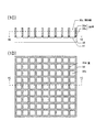
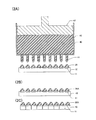
【解決手段】 半導体ウエハ(10)の表面に、複数の撮像素子(11)を形成する。撮像素子の各々の上に樹脂(35)を配置し、硬化させることにより、樹脂製の撮像レンズ(35B)を形成する。撮像レンズが形成された半導体ウエハを、撮像素子の各々と、その上に形成された撮像レンズとが一体になった撮像チップに分割する。
【選択図】 図1−4
Description
半導体ウエハの表面に、複数の撮像素子を形成する工程と、
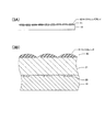
前記撮像素子の各々の上に樹脂を配置し、硬化させることにより、樹脂製の撮像レンズを形成する工程と、
前記撮像レンズが形成された前記半導体ウエハを、前記撮像素子の各々と、その上に形成された前記撮像レンズとが一体になった撮像チップに分割する工程と
を有する。
11 撮像素子
20 フォトダイオード
21 酸化シリコン膜
22 窒化シリコン膜
23 マイクロレンズ
30 枠
35 樹脂
35A 撮像レンズ
35B 尾根状突起
40 樹脂容器
41 射出口
42 ピストン
45 樹脂
48 金型
60 マイクロレンズアレイ
61 マイクロレンズ
Claims (4)
- 半導体ウエハの表面に、複数の撮像素子を形成する工程と、
前記撮像素子の各々の上に樹脂を配置し、硬化させることにより、樹脂製の撮像レンズを形成する工程と、
前記撮像レンズが形成された前記半導体ウエハを、前記撮像素子の各々と、その上に形成された前記撮像レンズとが一体になった撮像チップに分割する工程と
を有する固体撮像素子の製造方法。 - 前記撮像レンズを形成する工程が、
前記半導体ウエハの上に、前記撮像素子に対応した開口部を有する枠を配置する工程と、
前記枠の開口部内に樹脂を充填する工程と、
前記開口部内に、樹脂の表面を凸レンズ形状にする型を挿入して該樹脂を成型する工程と
を含む請求項1に記載の固体撮像素子の製造方法。 - 前記撮像レンズを形成する工程が、
前記撮像素子の上に、流動性を有する樹脂を、相互に隣り合う撮像素子の上に滴下された樹脂同士が連続しないように滴下し、該樹脂の表面張力により、滴下された樹脂の表面を凸状にする工程を含む請求項1に記載の固体撮像素子の製造方法。 - 前記流動性を有する樹脂を滴下する前に、前記撮像素子の各々の表面に該撮像素子の画素に対応した樹脂性のマイクロレンズを形成するとともに、該相互に隣り合う撮像素子の間には、無機材料が露出した状態とする請求項3に記載の固体撮像素子の製造方法。
Priority Applications (1)
| Application Number | Priority Date | Filing Date | Title |
|---|---|---|---|
| JP2008217048A JP5369542B2 (ja) | 2008-08-26 | 2008-08-26 | 固体撮像素子の製造方法 |
Applications Claiming Priority (1)
| Application Number | Priority Date | Filing Date | Title |
|---|---|---|---|
| JP2008217048A JP5369542B2 (ja) | 2008-08-26 | 2008-08-26 | 固体撮像素子の製造方法 |
Publications (2)
| Publication Number | Publication Date |
|---|---|
| JP2010056155A true JP2010056155A (ja) | 2010-03-11 |
| JP5369542B2 JP5369542B2 (ja) | 2013-12-18 |
Family
ID=42071786
Family Applications (1)
| Application Number | Title | Priority Date | Filing Date |
|---|---|---|---|
| JP2008217048A Expired - Fee Related JP5369542B2 (ja) | 2008-08-26 | 2008-08-26 | 固体撮像素子の製造方法 |
Country Status (1)
| Country | Link |
|---|---|
| JP (1) | JP5369542B2 (ja) |
Citations (3)
| Publication number | Priority date | Publication date | Assignee | Title |
|---|---|---|---|---|
| JP2002100758A (ja) * | 2000-07-06 | 2002-04-05 | Seiko Epson Corp | 機能ブロックを含む装置およびその製造方法ならびに光伝送装置 |
| JP2002290842A (ja) * | 2001-03-23 | 2002-10-04 | Sanyo Electric Co Ltd | 固体撮像素子の製造方法 |
| JP2005277311A (ja) * | 2004-03-26 | 2005-10-06 | Seiko Epson Corp | 受光素子、光電子集積素子、光モジュール、光伝達装置、および受光素子の製造方法 |
-
2008
- 2008-08-26 JP JP2008217048A patent/JP5369542B2/ja not_active Expired - Fee Related
Patent Citations (3)
| Publication number | Priority date | Publication date | Assignee | Title |
|---|---|---|---|---|
| JP2002100758A (ja) * | 2000-07-06 | 2002-04-05 | Seiko Epson Corp | 機能ブロックを含む装置およびその製造方法ならびに光伝送装置 |
| JP2002290842A (ja) * | 2001-03-23 | 2002-10-04 | Sanyo Electric Co Ltd | 固体撮像素子の製造方法 |
| JP2005277311A (ja) * | 2004-03-26 | 2005-10-06 | Seiko Epson Corp | 受光素子、光電子集積素子、光モジュール、光伝達装置、および受光素子の製造方法 |
Also Published As
| Publication number | Publication date |
|---|---|
| JP5369542B2 (ja) | 2013-12-18 |
Similar Documents
| Publication | Publication Date | Title |
|---|---|---|
| KR101087695B1 (ko) | 이종재료 일체형 렌즈 유닛 및 이를 구비하는 카메라 모듈 | |
| EP3081369B1 (en) | Method for manufacturing a lens | |
| US20080290435A1 (en) | Wafer level lens arrays for image sensor packages and the like, image sensor packages, and related methods | |
| US7944633B2 (en) | Lens holder for alignment of stacked lens module and manufacturing method thereof | |
| TWI617430B (zh) | 製造微透鏡之方法及裝置 | |
| EP2193911B1 (en) | Micro lens, method and apparatus for manufacturing micro lens, and camera module including micro lens | |
| US8294229B2 (en) | Wafer-scale array of optical packages and method for fabricating the same | |
| US9153614B2 (en) | Method and apparatus for lens alignment for optically sensitive devices and systems implementing same | |
| US7794633B2 (en) | Method and apparatus for fabricating lens masters | |
| WO2018023887A1 (zh) | 摄像模组及其模塑电路板组件和模塑感光组件和制造方法 | |
| TWM557454U (zh) | 攝像模組及其模塑電路板元件 | |
| CN107209342B (zh) | 相机模块的制造方法、像面侧组透镜、像面侧组透镜的制造方法和摄像元件 | |
| US8828174B2 (en) | Method of manufacturing a plurality of optical devices | |
| TWM557833U (zh) | 攝像模組、模塑感光元件、成型模具及其電子設備 | |
| WO2019062609A1 (zh) | 摄像模组、感光组件、感光组件拼板及其成型模具和制造方法 | |
| KR100817060B1 (ko) | 카메라 모듈 및 그 제조 방법 | |
| TWI453111B (zh) | 影像感測元件之製造方法及鑄造裝置 | |
| JP2010173196A (ja) | 成形方法、成形装置、成形金型、光学素子アレイ板の製造方法、電子素子モジュールの製造方法、電子情報機器 | |
| CN111133742B (zh) | 摄像模组、感光组件、感光组件拼板及其成型模具和制造方法 | |
| US20100123260A1 (en) | Stamp with mask pattern for discrete lens replication | |
| JP5369542B2 (ja) | 固体撮像素子の製造方法 | |
| WO2013047653A1 (ja) | 撮像レンズユニット及び撮像レンズユニットの製造方法 | |
| US20080198481A1 (en) | Aspheric lens structures and fabrication methods thereof | |
| CN106646808A (zh) | 相机模块 | |
| JP3154933U (ja) | スタックレンズモジュールの位置決めレンズホルダー |
Legal Events
| Date | Code | Title | Description |
|---|---|---|---|
| A621 | Written request for application examination |
Free format text: JAPANESE INTERMEDIATE CODE: A621 Effective date: 20110511 |
|
| A131 | Notification of reasons for refusal |
Free format text: JAPANESE INTERMEDIATE CODE: A131 Effective date: 20130212 |
|
| A977 | Report on retrieval |
Free format text: JAPANESE INTERMEDIATE CODE: A971007 Effective date: 20130214 |
|
| A521 | Request for written amendment filed |
Free format text: JAPANESE INTERMEDIATE CODE: A523 Effective date: 20130404 |
|
| TRDD | Decision of grant or rejection written | ||
| A01 | Written decision to grant a patent or to grant a registration (utility model) |
Free format text: JAPANESE INTERMEDIATE CODE: A01 Effective date: 20130820 |
|
| A61 | First payment of annual fees (during grant procedure) |
Free format text: JAPANESE INTERMEDIATE CODE: A61 Effective date: 20130902 |
|
| R150 | Certificate of patent or registration of utility model |
Ref document number: 5369542 Country of ref document: JP Free format text: JAPANESE INTERMEDIATE CODE: R150 Free format text: JAPANESE INTERMEDIATE CODE: R150 |
|
| S531 | Written request for registration of change of domicile |
Free format text: JAPANESE INTERMEDIATE CODE: R313531 |
|
| R350 | Written notification of registration of transfer |
Free format text: JAPANESE INTERMEDIATE CODE: R350 |
|
| LAPS | Cancellation because of no payment of annual fees |