JP2010050288A - Resin-sealed semiconductor device and method of manufacturing the same - Google Patents
Resin-sealed semiconductor device and method of manufacturing the same Download PDFInfo
- Publication number
- JP2010050288A JP2010050288A JP2008213409A JP2008213409A JP2010050288A JP 2010050288 A JP2010050288 A JP 2010050288A JP 2008213409 A JP2008213409 A JP 2008213409A JP 2008213409 A JP2008213409 A JP 2008213409A JP 2010050288 A JP2010050288 A JP 2010050288A
- Authority
- JP
- Japan
- Prior art keywords
- resin
- heat sink
- semiconductor device
- gnd
- relay electrode
- Prior art date
- Legal status (The legal status is an assumption and is not a legal conclusion. Google has not performed a legal analysis and makes no representation as to the accuracy of the status listed.)
- Withdrawn
Links
Images


Classifications
-
- H—ELECTRICITY
- H01—ELECTRIC ELEMENTS
- H01L—SEMICONDUCTOR DEVICES NOT COVERED BY CLASS H10
- H01L2224/00—Indexing scheme for arrangements for connecting or disconnecting semiconductor or solid-state bodies and methods related thereto as covered by H01L24/00
- H01L2224/01—Means for bonding being attached to, or being formed on, the surface to be connected, e.g. chip-to-package, die-attach, "first-level" interconnects; Manufacturing methods related thereto
- H01L2224/26—Layer connectors, e.g. plate connectors, solder or adhesive layers; Manufacturing methods related thereto
- H01L2224/31—Structure, shape, material or disposition of the layer connectors after the connecting process
- H01L2224/32—Structure, shape, material or disposition of the layer connectors after the connecting process of an individual layer connector
- H01L2224/321—Disposition
- H01L2224/32151—Disposition the layer connector connecting between a semiconductor or solid-state body and an item not being a semiconductor or solid-state body, e.g. chip-to-substrate, chip-to-passive
- H01L2224/32221—Disposition the layer connector connecting between a semiconductor or solid-state body and an item not being a semiconductor or solid-state body, e.g. chip-to-substrate, chip-to-passive the body and the item being stacked
- H01L2224/32225—Disposition the layer connector connecting between a semiconductor or solid-state body and an item not being a semiconductor or solid-state body, e.g. chip-to-substrate, chip-to-passive the body and the item being stacked the item being non-metallic, e.g. insulating substrate with or without metallisation
-
- H—ELECTRICITY
- H01—ELECTRIC ELEMENTS
- H01L—SEMICONDUCTOR DEVICES NOT COVERED BY CLASS H10
- H01L2224/00—Indexing scheme for arrangements for connecting or disconnecting semiconductor or solid-state bodies and methods related thereto as covered by H01L24/00
- H01L2224/01—Means for bonding being attached to, or being formed on, the surface to be connected, e.g. chip-to-package, die-attach, "first-level" interconnects; Manufacturing methods related thereto
- H01L2224/42—Wire connectors; Manufacturing methods related thereto
- H01L2224/47—Structure, shape, material or disposition of the wire connectors after the connecting process
- H01L2224/48—Structure, shape, material or disposition of the wire connectors after the connecting process of an individual wire connector
- H01L2224/481—Disposition
- H01L2224/48151—Connecting between a semiconductor or solid-state body and an item not being a semiconductor or solid-state body, e.g. chip-to-substrate, chip-to-passive
- H01L2224/48221—Connecting between a semiconductor or solid-state body and an item not being a semiconductor or solid-state body, e.g. chip-to-substrate, chip-to-passive the body and the item being stacked
- H01L2224/48225—Connecting between a semiconductor or solid-state body and an item not being a semiconductor or solid-state body, e.g. chip-to-substrate, chip-to-passive the body and the item being stacked the item being non-metallic, e.g. insulating substrate with or without metallisation
- H01L2224/48227—Connecting between a semiconductor or solid-state body and an item not being a semiconductor or solid-state body, e.g. chip-to-substrate, chip-to-passive the body and the item being stacked the item being non-metallic, e.g. insulating substrate with or without metallisation connecting the wire to a bond pad of the item
-
- H—ELECTRICITY
- H01—ELECTRIC ELEMENTS
- H01L—SEMICONDUCTOR DEVICES NOT COVERED BY CLASS H10
- H01L2224/00—Indexing scheme for arrangements for connecting or disconnecting semiconductor or solid-state bodies and methods related thereto as covered by H01L24/00
- H01L2224/01—Means for bonding being attached to, or being formed on, the surface to be connected, e.g. chip-to-package, die-attach, "first-level" interconnects; Manufacturing methods related thereto
- H01L2224/42—Wire connectors; Manufacturing methods related thereto
- H01L2224/47—Structure, shape, material or disposition of the wire connectors after the connecting process
- H01L2224/48—Structure, shape, material or disposition of the wire connectors after the connecting process of an individual wire connector
- H01L2224/481—Disposition
- H01L2224/48151—Connecting between a semiconductor or solid-state body and an item not being a semiconductor or solid-state body, e.g. chip-to-substrate, chip-to-passive
- H01L2224/48221—Connecting between a semiconductor or solid-state body and an item not being a semiconductor or solid-state body, e.g. chip-to-substrate, chip-to-passive the body and the item being stacked
- H01L2224/48245—Connecting between a semiconductor or solid-state body and an item not being a semiconductor or solid-state body, e.g. chip-to-substrate, chip-to-passive the body and the item being stacked the item being metallic
- H01L2224/48247—Connecting between a semiconductor or solid-state body and an item not being a semiconductor or solid-state body, e.g. chip-to-substrate, chip-to-passive the body and the item being stacked the item being metallic connecting the wire to a bond pad of the item
-
- H—ELECTRICITY
- H01—ELECTRIC ELEMENTS
- H01L—SEMICONDUCTOR DEVICES NOT COVERED BY CLASS H10
- H01L2224/00—Indexing scheme for arrangements for connecting or disconnecting semiconductor or solid-state bodies and methods related thereto as covered by H01L24/00
- H01L2224/01—Means for bonding being attached to, or being formed on, the surface to be connected, e.g. chip-to-package, die-attach, "first-level" interconnects; Manufacturing methods related thereto
- H01L2224/42—Wire connectors; Manufacturing methods related thereto
- H01L2224/47—Structure, shape, material or disposition of the wire connectors after the connecting process
- H01L2224/49—Structure, shape, material or disposition of the wire connectors after the connecting process of a plurality of wire connectors
- H01L2224/491—Disposition
- H01L2224/4912—Layout
- H01L2224/49171—Fan-out arrangements
-
- H—ELECTRICITY
- H01—ELECTRIC ELEMENTS
- H01L—SEMICONDUCTOR DEVICES NOT COVERED BY CLASS H10
- H01L2224/00—Indexing scheme for arrangements for connecting or disconnecting semiconductor or solid-state bodies and methods related thereto as covered by H01L24/00
- H01L2224/73—Means for bonding being of different types provided for in two or more of groups H01L2224/10, H01L2224/18, H01L2224/26, H01L2224/34, H01L2224/42, H01L2224/50, H01L2224/63, H01L2224/71
- H01L2224/732—Location after the connecting process
- H01L2224/73251—Location after the connecting process on different surfaces
- H01L2224/73265—Layer and wire connectors
Abstract
Description
本発明は、樹脂封止型半導体装置およびその製造方法に関し、特に半導体素子を放熱板上に搭載しリードに接続した樹脂封止型半導体装置およびその製造方法に関する。 The present invention relates to a resin-encapsulated semiconductor device and a method for manufacturing the same, and more particularly to a resin-encapsulated semiconductor device in which a semiconductor element is mounted on a heat sink and connected to leads, and a method for manufacturing the same.
従来の樹脂封止型半導体装置の断面を図7に示す。半導体素子11を搭載するアイランド部21の周辺端部に、リード16のインナーリード部分と相対位する中継電極部6を個々に絶縁して形成することで、半導体素子11が小さくてリード16との間隔が大きくても、内部結線するワイヤ23を短くし、安定したワイヤループが形成できるようにしている。3は絶縁材料、22は封止樹脂である(特許文献1)。複数の半導体素子のGNDを共有化させ、外部端子数の削減を図るためのバーリードを形成したものもある(特許文献2)。
電子機器の小型化、高速化が進むに伴い、半導体装置の小型化、実装面積の縮小化、および高放熱特性を備えることが要求されている。近年では、マイコン素子とメモリ素子の双方を1つの半導体装置に収納するSiP構造の開発が盛んに行われており、放熱板上に多チップを搭載することが検討、実用化されている。 As electronic devices become smaller and faster, semiconductor devices are required to be smaller, smaller in mounting area, and to have high heat dissipation characteristics. In recent years, an SiP structure in which both a microcomputer element and a memory element are accommodated in one semiconductor device has been actively developed, and mounting and mounting of multiple chips on a heat sink has been studied and put into practical use.
ここで、放熱板上に特許文献1,2に記載された中継電極部やGNDを配置することが考えられる。しかし、特許文献1に記載された中継電極部を設けるためには一般に、絶縁材料上にマスクパターンを形成し、更に絶縁材料上に導電膜を物理的に蒸着する必要があり、製作工程数が増加し、コストが上昇する。また中継電極部をインナーリードと相対位させるので、複数の半導体素子を搭載する場合、互いの半導体素子寄りのパッド部についてはワイヤ配線が制限され、ロングワイヤが必要となる。またこの場合、GND端子の共通化はできない。
Here, it is conceivable to arrange the relay electrode part and GND described in
一方、特許文献2に記載された半導体装置の構造では、中継できる配線層がないためロングワイヤが必要となる。また意図したことではあるが、共通のリードバーを設けるので、外部出力の端子数が制限される。さらに、予めGNDとなる外部出力端子を想定した設計が必要であり、品種毎に専用のリードフレームの製作が必要となる。
On the other hand, the structure of the semiconductor device described in
本発明は、上記問題に鑑み、放熱板上に複数の半導体素子を搭載してもワイヤ配線の自由度が高く、製作も容易な樹脂封止型半導体装置を提供することを目的とする。 In view of the above problems, an object of the present invention is to provide a resin-encapsulated semiconductor device that has a high degree of freedom in wire wiring and can be easily manufactured even if a plurality of semiconductor elements are mounted on a heat sink.
上記課題を解決するために本発明は、複数の半導体素子と、前記半導体素子を搭載した放熱板と、前記放熱板とは別体に形成され前記半導体素子とワイヤを介して接続されたリードと、前記半導体素子を封止した樹脂封止体とを有した樹脂封止型半導体装置を製造する際に、前記放熱板に予め、前記ワイヤのための中継電極部およびGND部が一体にパターニングされた配線板を絶縁材料と導電材料とを用いて貼り合わせ、この配線板をパンチングして個々の中継電極部およびGND部に分離することを特徴とする。 In order to solve the above problems, the present invention includes a plurality of semiconductor elements, a heat sink on which the semiconductor elements are mounted, and leads formed separately from the heat sink and connected to the semiconductor elements through wires. When manufacturing a resin-encapsulated semiconductor device having a resin-encapsulated body in which the semiconductor element is encapsulated, the relay electrode portion and the GND portion for the wire are integrally patterned in advance on the heat sink. The wiring board is bonded using an insulating material and a conductive material, and the wiring board is punched to be separated into individual relay electrode portions and GND portions.
予めパターニングされた配線板を導電材料および絶縁材料を用いて放熱板に貼り合わせてから分割するというもので、一度の貼り合わせで、絶縁された中継部(中継電極部)と放熱板に導通した中継部(GND部)とを形成することができる。これにより、工程数の削減、低価格化が可能となる。中継部の位置を適切にすれば、複数の半導体素子を搭載する場合もワイヤ配線の自由度が高く、また外部出力端子数を削減できる。 A pre-patterned wiring board is bonded to a heat sink using a conductive material and an insulating material, and then divided, and is electrically connected to the insulated relay section (relay electrode section) and the heat sink by a single bonding. A relay part (GND part) can be formed. Thereby, the number of processes can be reduced and the price can be reduced. If the position of the relay portion is appropriate, the degree of freedom of wire wiring is high even when a plurality of semiconductor elements are mounted, and the number of external output terminals can be reduced.
配線板と同時に放熱板をパンチングして前記放熱板に開口部を形成することが好ましい。配線板は放熱板よりも板厚が薄いことが好ましい。
上記のように製造される本発明の樹脂封止型半導体装置は、複数の半導体素子と、前記半導体素子を搭載した放熱板と、前記放熱板とは別体に形成され前記半導体素子とワイヤを介して接続されたリードと、前記半導体素子を封止した樹脂封止体とを有した樹脂封止型半導体装置において、前記放熱板に、同一の板材からなる前記ワイヤのための中継電極部およびGND部が各々、絶縁材料または導電材料を用いて設けられていることを特徴とする。
It is preferable to punch the heat sink simultaneously with the wiring board to form an opening in the heat sink. The wiring board is preferably thinner than the heat sink.
The resin-encapsulated semiconductor device of the present invention manufactured as described above includes a plurality of semiconductor elements, a heat sink on which the semiconductor elements are mounted, and the heat sink. In a resin-encapsulated semiconductor device having a lead connected via a resin encapsulant that encapsulates the semiconductor element, a relay electrode portion for the wire made of the same plate material and the heat sink Each of the GND portions is provided using an insulating material or a conductive material.
導電材料および絶縁材料は260℃以上の融点を有するることが好ましい。中継部の表面にAuまたはAgまたはPdによるめっき処理が施されていることが好ましい。
放熱板上での中継電極部およびGND部の上面の高さが同一であることが好ましい。放熱板上での中継電極部およびGND部の上面がリードのワイヤ接続面よりも低位にあることが好ましい。放熱板の中央部に半導体素子が搭載され、前記放熱板の周縁部にGND部が配置されることが都合よい。
The conductive material and the insulating material preferably have a melting point of 260 ° C. or higher. It is preferable that the surface of the relay portion is plated with Au, Ag, or Pd.
It is preferable that the height of the upper surface of the relay electrode part and the GND part on the heat sink is the same. It is preferable that the upper surfaces of the relay electrode portion and the GND portion on the heat sink are lower than the wire connection surface of the lead. Conveniently, a semiconductor element is mounted at the center of the heat sink, and a GND portion is disposed at the peripheral edge of the heat sink.
本発明によれば、パターニングされた配線板を放熱板上に導電材料と絶縁材料とを用いて接続することにより、放熱板上に複数の配線を製造する工程を不要として、中継電極部や共通のGND部となる中継部(配線層)を容易に安価に形成することができ、外部出力端子の数を少なくできるとともに、中継部によってワイヤの配線自由度も向上できる。また放熱板上で半導体素子を中継電極部やGND部で囲んだ形とすれば、放熱板を内蔵した樹脂封止型半導体装置の課題であるパッケージの反りを低減できる。 According to the present invention, the step of manufacturing a plurality of wirings on the heat sink is unnecessary by connecting the patterned wiring board on the heat sink using a conductive material and an insulating material, so that the relay electrode portion and the common The relay portion (wiring layer) to be the GND portion can be easily formed at low cost, the number of external output terminals can be reduced, and the wiring wiring flexibility can be improved by the relay portion. Further, if the semiconductor element is surrounded by the relay electrode portion and the GND portion on the heat sink, the warpage of the package, which is a problem of the resin-encapsulated semiconductor device having the heat sink built therein, can be reduced.
本発明の実施の形態について図面を参照して説明する。
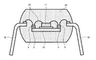
図1(a)は本発明の一実施形態の樹脂封止型半導体装置の平面図、図1(b)は同樹脂封止型半導体装置の図1(a)におけるA−A’断面図である。ここでは理解を容易にするために封止樹脂を除いて図示している。
Embodiments of the present invention will be described with reference to the drawings.
1A is a plan view of a resin-encapsulated semiconductor device according to an embodiment of the present invention, and FIG. 1B is a cross-sectional view taken along the line AA ′ of FIG. 1A of the resin-encapsulated semiconductor device. is there. Here, for ease of understanding, the sealing resin is not shown.
複数(ここでは2個)の半導体素子11が放熱板1上に搭載されており、各半導体素子11はワイヤ8(8a〜8d)を介して複数のリード16(インナーリード部分のみ示す)に電気的に接続されている。
A plurality (two in this case) of
放熱板1は一般に銅または銅合金から製作され、GND部5や中継電極部6といった配線層が片面に形成されている。放熱板1の周縁部分であって前記配線層の外周部分にはスリット部7が形成されている。
The
GND部5および中継電極部6は、銅または銅合金、鉄または鉄合金からなる同一の板材で形成されていて、GND部5は導電材料4を用いて、中継電極部6は絶縁材料3を用いて放熱板1に貼り付けられている。
The
複数のリード16は、放熱板1とは別体をなすもので、放熱板1の端辺に沿う方向に適当間隔をあけて配列されていて、各々、放熱板1の端部に絶縁材料3により接合されている。
The plurality of
各半導体素子11は複数の電極部を有しており、放熱板1の中央部に接着剤10により固着されていて、ワイヤ8(8a〜8d)によって、中継電極部6あるいはGND部5を介してあるいは直接にリード16に接続されている。
Each
上記の樹脂封止型半導体装置の製造方法を図2を参照して説明する。
図2(a)(b)に示すように、放熱板1の所定の接合箇所に印刷またはポッティングにより導電材料4および絶縁材料3を塗布し、その上に配線板2を位置合わせして搭載し、加熱および加圧して貼り付ける。放熱板1ではなく配線板2に導電材料4および絶縁材料3を塗布しても構わない。
A method for manufacturing the resin-encapsulated semiconductor device will be described with reference to FIG.
As shown in FIGS. 2 (a) and 2 (b), the
配線板2は、上述のGND部5および中継電極部6を接続部12、支持リード13により一体化して、エッチング、パンチング加工等によってパターニングしたもので、放熱板1よりも面積が小さく、表面にはワイヤボンド接合のために必要な導電膜(図示せず)が皮膜処理によって形成されている。
The
導電材料4および絶縁材料3は、完成品を実装基板に実装する時の温度(260℃)よりも高い融点の材料が用いられる。導電材料4は例えばBi-Cu系はんだ、絶縁材料3は例えばポリイミド樹脂である。各々の塗布量は、望ましくは、配線板2の貼り付け後に中継電極部6およびGND部5への投影面積が同等またはそれ以下となる量とする。ショートやブリッジを防止するためである。
As the
塗布終了後に、望ましくは、中継電極部6やGND部5の上面が放熱板1に対して並行となるように、つまり導電材料4および絶縁材料3の厚みが均一になるように加熱および加圧する。ワイヤ接続時の接合信頼性を向上するためである。
After the application, desirably, heating and pressurization are performed so that the upper surfaces of the
次に、図2(c)(d)に示すように、配線板2の支持リード13を治具18でパンチングカットして、中継電極部6およびGND部5をそれぞれ独立させる。同時に放熱板1の支持リード13相応部分も打ち抜いてスリット部7を形成する。
Next, as shown in FIGS. 2 (c) and 2 (d), the support leads 13 of the
この後に、望ましくは、図2(e)に示すように、スリット部7を起点として放熱板1の一部をアップセットするか、あるいは、図2(f)に示すように、スリット部7を起点として放熱板1の一部をダウンセットする。
Thereafter, preferably, as shown in FIG. 2 (e), a part of the
再び図1(a)(b)を参照する。以上のようにして作成した配線板2と放熱板1との接合体を、リードフレームのリード16に絶縁材料3を用いて接合する。そしてこの接合体の放熱板1上に半導体素子11,11を接着剤10を用いて固着する。
Reference is again made to FIGS. The joined body of the
次に、各半導体素子11からリード16へワイヤ配線を行う。この時の配線の自由度を向上させるために、中継電極部6およびGND部5が形成されている。たとえば、半導体素子11からのワイヤ8aを中継電極部6に接合し、中継電極部6からのワイヤ8bをリード16へ接続する。このようにすることにより、半導体素子11から離れたリード16へ直接にワイヤ接続する場合に比べて、ワイヤ8a,8bのワイヤ長を短くすることができる。ワイヤコストも低減できる。
Next, wire wiring is performed from each
また半導体素子11から必要な本数のワイヤ8cを共通のGND部5に接続し、GND部5からのワイヤ8dをリード16へ接続する。このようにGND部5を共通化すること、また図示したように半導体素子11を囲む形状としておくことで、ワイヤ接続可能なリード16の選択範囲が増加し、ワイヤ本数を削減できる。
Further, the necessary number of
ワイヤ接続の終了後に、半導体素子11、中継電極部6,GND部5などの配線層、放熱板1、ワイヤ8(8a,8b,8c,8d)、リード16の一端部を樹脂モールドする。この際に、金属ワイヤ8のワイヤ長を短くしていることにより、モールド金型への樹脂注入時のワイヤ流れ等を抑えることができ、短絡を防止することが可能となる。また放熱板1にスリット部7を設けてあることにより、封止樹脂の流動特性が向上しボイドや未充填などが防止されると共に、封止樹脂がスリット部7に入り込んで放熱板1との密着性が向上する。
After the end of the wire connection, the
図3は以上のようにして作製した樹脂封止型半導体装置14を実装基板15に実装した状態で示している。半導体素子11の周りをGND部5および中継電極部6が取り囲んだ形、見かけ上は半導体素子11が放熱板1側に入り込んだ形となっている。このため放熱板1上に蒸着等で配線層やGND層を形成する従来方式と比べて、放熱板1の剛性強度が増大し、放熱板1を内蔵した樹脂封止型半導体装置の課題であったパッケージ反りを低減することができる。
FIG. 3 shows a state in which the resin-encapsulated
また絶縁材料3および導電材料4に融点260℃以上の材料を用いているため、実装基板15にリフローやフロー工法で実装する時に一般的に用いるはんだ材料17(融点220℃程度のSn−Ag−Cu系の鉛フリーはんだ材料)を溶融させる際に、絶縁材料3や導電材料4が溶融することはなく、かかる溶融に伴う体積膨張によって中継電極部6とGND部5とが接触したり、パッケージクラックが発生するといった不具合は発生しない。
Since the insulating
また、図示したようにスリット部7を起点として放熱板1の端部をアップセット(あるいはダウンセット)することで、封止樹脂22中での放熱板1の位置を自由に変更することができ、半導体素子11と放熱板1との上下両側の樹脂厚を均等にすることができる。ダウンセットの場合は、半導体素子11上に別の半導体素子を積層しても、最上層の半導体素子上の樹脂厚と放熱板1の下の樹脂厚とを同等にすることが可能となる。このことにより、ワイヤ8の露出を防ぎ、封止樹脂22による応力を低減してパッケージの反りを抑制し、クラック等の信頼性を向上できるとともに、はんだ耐熱性などの信頼性を向上させることができる。
Further, as shown in the figure, the position of the
中継電極部6およびGND部5の上面を半導体素子11の最上面よりも低くすることにより、中継電極部6およびGND部5の平坦性、つまり放熱板1に対する中継電極部6およびGND部5の平行度が向上することになり、このことによってもワイヤ配線時の接合信頼性が向上する。
By making the upper surfaces of the
中継電極部6およびGND部5の上面をリード16のワイヤ接続面よりも下位に存在させることにより、半導体素子11からリード16にワイヤ配線する際にワイヤがGND部5に接触するのを防止できる。
By making the upper surfaces of the
図4は、パンチングカットを実施する前の放熱板1と配線板2との接合体の平面図である。放熱板1の中央部に2個の半導体素子11の搭載領域が間隔をあけて設定されている。配線板2には、2個の半導体素子11の搭載領域の間に配置された中継電極部6と、各半導体素子11の搭載領域の三方を囲むように中継電極部6の両側にそれぞれコの字形に配置されたGND部5と、GND部5の外側に放熱板1の端辺に沿う方向に配置された支持リード13と、中継電極部6およびGND部5を支持リード13に接続した複数の接続部12とが一体にパターニングされている。
FIG. 4 is a plan view of a joined body of the
支持リード13は、中継電極部6およびGND部5を形成する上で表面処理や取り扱い強度を向上させるために設けられるもので、これら中継電極部6およびGND部5が放熱板1上に接合された後には不要である。この支持リード13を上述のようにパンチングカットすることで、中継電極部6とGND部5とが個々に分離される。この際に放熱板1も同時に打ち抜かれて、仮想線で示したように支持リード13より一回り大きいスリット部7が形成される。支持リード13と中継電極部6およびGND部5とを接続した接続部12の接続幅W1は、配線板2の厚みより薄くしておくことが好ましく、それによりパンチングカット時の応力を低減できる。放熱板1も同時に打ち抜くのは、カット部分が放熱板1に接触しないようにするためでもある。
The
図5に、放熱板1上に導電材料4および絶縁材料3を介して加熱および加圧により接続させた中継電極部6およびGND部5の拡大断面図を示す。
パターニング後の中継電極部6およびGND部5の最表面に表面層20をAu(好ましくは、20〜70オングストローム)またはAg(2ミクロン以上)またはPd(0.02ミクロン以上)をめっき処理により形成している。このような表面層20を有することで、ワイヤ配線を容易化できると共に、ワイヤ配線後の接続信頼性を向上させることができる。
FIG. 5 shows an enlarged cross-sectional view of the
A
ただし、中継電極部6と絶縁材料3との接合強度、および、GND部5と導電材料4との接合強度を増加させるために、中継電極部6と絶縁材料3との界面、および、GND部5と導電材料4との界面にめっき処理を施こさないこともできる。
However, in order to increase the bonding strength between the
図6に、放熱板1上に導電材料4および絶縁材料3を介して加熱および加圧により接続させた中継電極部6およびGND部5の他の拡大断面図を示す。
放熱板1の厚みB(例えば、0.2mm)に対して、配線板2(中継電極部6およびGND部5)の厚みB´を薄くしている(約80ミクロン〜150ミクロン)。このことにより、パンチングカットに要する力を少なくし、配線板2の位置精度を確保すると共に、パターニング時に配線板2の線幅W2を細くすることで配線密度をあげ、中継電極部6やGND部5の数を増やすことが可能となる。
FIG. 6 shows another enlarged cross-sectional view of the
The thickness B ′ of the wiring board 2 (the
また放熱板1上での配線板2の中継電極部6の高さCとGND部5の高さC´とを同一にしている。このことにより、ワイヤ配線時の接続信頼性が向上する。樹脂封止型半導体装置14の熱時の反りも低減できる。
Further, the height C of the
本発明の樹脂封止型半導体装置の構造および製造方法は、放熱性が要求される装置に特に好適に適用できる。 The structure and manufacturing method of the resin-encapsulated semiconductor device of the present invention can be particularly suitably applied to a device that requires heat dissipation.
1 放熱板
2 配線板
3 絶縁材料
4 導電材料
5 GND部
6 中継電極部
7 スリット部
8 ワイヤ
11 半導体素子
13 支持リード
14 樹脂封止型半導体装置
15 実装基板
16 リード
17 はんだ材料
18 治具
20 表面層
22 封止樹脂
DESCRIPTION OF
Claims (9)
Priority Applications (1)
| Application Number | Priority Date | Filing Date | Title |
|---|---|---|---|
| JP2008213409A JP2010050288A (en) | 2008-08-22 | 2008-08-22 | Resin-sealed semiconductor device and method of manufacturing the same |
Applications Claiming Priority (1)
| Application Number | Priority Date | Filing Date | Title |
|---|---|---|---|
| JP2008213409A JP2010050288A (en) | 2008-08-22 | 2008-08-22 | Resin-sealed semiconductor device and method of manufacturing the same |
Publications (2)
| Publication Number | Publication Date |
|---|---|
| JP2010050288A true JP2010050288A (en) | 2010-03-04 |
| JP2010050288A5 JP2010050288A5 (en) | 2011-08-04 |
Family
ID=42067137
Family Applications (1)
| Application Number | Title | Priority Date | Filing Date |
|---|---|---|---|
| JP2008213409A Withdrawn JP2010050288A (en) | 2008-08-22 | 2008-08-22 | Resin-sealed semiconductor device and method of manufacturing the same |
Country Status (1)
| Country | Link |
|---|---|
| JP (1) | JP2010050288A (en) |
Cited By (3)
| Publication number | Priority date | Publication date | Assignee | Title |
|---|---|---|---|---|
| CN106298723A (en) * | 2015-05-13 | 2017-01-04 | 无锡华润安盛科技有限公司 | A kind of twin islet lead frame framework |
| CN109564918A (en) * | 2016-08-10 | 2019-04-02 | 三菱电机株式会社 | Semiconductor device |
| CN115346948A (en) * | 2022-10-14 | 2022-11-15 | 吉光半导体(绍兴)有限公司 | Half-bridge module |
-
2008
- 2008-08-22 JP JP2008213409A patent/JP2010050288A/en not_active Withdrawn
Cited By (4)
| Publication number | Priority date | Publication date | Assignee | Title |
|---|---|---|---|---|
| CN106298723A (en) * | 2015-05-13 | 2017-01-04 | 无锡华润安盛科技有限公司 | A kind of twin islet lead frame framework |
| CN109564918A (en) * | 2016-08-10 | 2019-04-02 | 三菱电机株式会社 | Semiconductor device |
| CN109564918B (en) * | 2016-08-10 | 2023-09-29 | 三菱电机株式会社 | Semiconductor device with a semiconductor device having a plurality of semiconductor chips |
| CN115346948A (en) * | 2022-10-14 | 2022-11-15 | 吉光半导体(绍兴)有限公司 | Half-bridge module |
Similar Documents
| Publication | Publication Date | Title |
|---|---|---|
| US5874784A (en) | Semiconductor device having external connection terminals provided on an interconnection plate and fabrication process therefor | |
| KR970010678B1 (en) | Lead frame and the package thereof | |
| US6621152B2 (en) | Thin, small-sized power semiconductor package | |
| US9385072B2 (en) | Method of manufacturing semiconductor device and semiconductor device | |
| US20040080025A1 (en) | Lead frame, method of manufacturing the same, and semiconductor device manufactured with the same | |
| US8133759B2 (en) | Leadframe | |
| JP2005191240A (en) | Semiconductor device and method for manufacturing the same | |
| KR20060121823A (en) | Reversible leadless package and methods of making and using same | |
| JP5100967B2 (en) | Lead frame, semiconductor chip package using the same, and manufacturing method thereof | |
| JPH04280462A (en) | Lead frame and semiconductor device using this lead frame | |
| US20070130759A1 (en) | Semiconductor device package leadframe formed from multiple metal layers | |
| JP2003017524A (en) | Method for manufacturing resin sealed semiconductor device | |
| JP2005244035A (en) | Mounting method of semiconductor device, and semiconductor device | |
| US10943857B2 (en) | Substrate with multi-layer resin structure and semiconductor device including the substrate | |
| US20040262752A1 (en) | Semiconductor device | |
| JP2010050288A (en) | Resin-sealed semiconductor device and method of manufacturing the same | |
| JP5621712B2 (en) | Semiconductor chip | |
| KR101753416B1 (en) | Leadframe for ic package and method of manufacture | |
| JP2006279088A (en) | Method for manufacturing semiconductor device | |
| JP2015153987A (en) | mold package | |
| JP4732138B2 (en) | Semiconductor device and manufacturing method thereof | |
| JP2009224529A (en) | Semiconductor device and its manufacturing method | |
| JP2005311099A (en) | Semiconductor device and its manufacturing method | |
| JP2007141947A (en) | Semiconductor device and its manufacturing method | |
| WO2021020456A1 (en) | Semiconductor package and semiconductor device |
Legal Events
| Date | Code | Title | Description |
|---|---|---|---|
| A521 | Request for written amendment filed |
Free format text: JAPANESE INTERMEDIATE CODE: A523 Effective date: 20110615 |
|
| A621 | Written request for application examination |
Free format text: JAPANESE INTERMEDIATE CODE: A621 Effective date: 20110615 |
|
| A761 | Written withdrawal of application |
Free format text: JAPANESE INTERMEDIATE CODE: A761 Effective date: 20110916 |