JP2010045391A - Method of manufacturing layered structure, semiconductor substrate, method of manufacturing element circuit, and serial connection circuit of solar cell element - Google Patents
Method of manufacturing layered structure, semiconductor substrate, method of manufacturing element circuit, and serial connection circuit of solar cell element Download PDFInfo
- Publication number
- JP2010045391A JP2010045391A JP2009258859A JP2009258859A JP2010045391A JP 2010045391 A JP2010045391 A JP 2010045391A JP 2009258859 A JP2009258859 A JP 2009258859A JP 2009258859 A JP2009258859 A JP 2009258859A JP 2010045391 A JP2010045391 A JP 2010045391A
- Authority
- JP
- Japan
- Prior art keywords
- layered structure
- layer
- semiconductor substrate
- porous layer
- porous
- Prior art date
- Legal status (The legal status is an assumption and is not a legal conclusion. Google has not performed a legal analysis and makes no representation as to the accuracy of the status listed.)
- Granted
Links
Images


Classifications
-
- Y—GENERAL TAGGING OF NEW TECHNOLOGICAL DEVELOPMENTS; GENERAL TAGGING OF CROSS-SECTIONAL TECHNOLOGIES SPANNING OVER SEVERAL SECTIONS OF THE IPC; TECHNICAL SUBJECTS COVERED BY FORMER USPC CROSS-REFERENCE ART COLLECTIONS [XRACs] AND DIGESTS
- Y02—TECHNOLOGIES OR APPLICATIONS FOR MITIGATION OR ADAPTATION AGAINST CLIMATE CHANGE
- Y02E—REDUCTION OF GREENHOUSE GAS [GHG] EMISSIONS, RELATED TO ENERGY GENERATION, TRANSMISSION OR DISTRIBUTION
- Y02E10/00—Energy generation through renewable energy sources
- Y02E10/50—Photovoltaic [PV] energy
- Y02E10/547—Monocrystalline silicon PV cells
Landscapes
- Photovoltaic Devices (AREA)
Abstract
Description
本発明は、多孔性物質層(中空キャビティを有する物質層を含む)が例えば単結晶pタイプまたはnタイプSiから成る基板上に生成され、更に層状構造体あるいはその一部が多孔性物質層(多孔性層)に順次設けられ、また例えば多孔性層内、または多孔性層と層状構造体との境界面で、機械的歪みが生成されている間に目的の破砕位置として多孔性層を使用する、基板から順次分離される層状構造体の製造方法、また半導体基板、素子回路製造方法、さらに太陽電池素子の直列接続回路に関する。 In the present invention, a porous material layer (including a material layer having a hollow cavity) is formed on a substrate made of, for example, single-crystal p-type or n-type Si, and a layered structure or a part thereof is a porous material layer ( The porous layer is used as a target crushing position while mechanical strain is generated, for example, in the porous layer or at the interface between the porous layer and the layered structure. The present invention also relates to a method for manufacturing a layered structure sequentially separated from a substrate, a semiconductor substrate, an element circuit manufacturing method, and a series connection circuit of solar cell elements.
最初に挙げた種類の方法は、複数の文書により公知である。 The first type of method is known from documents.
半導体本体の製造方法は、特許文献1に例を挙げて説明されており、その中ではシリコン基板は多孔性に生成され、非多孔性の単結晶シリコン層は第1温度で多孔性シリコン基板上に形成され、また非多孔性単結晶シリコン層はその表面に絶縁体を有する第2基板に接合される。その後、多孔性シリコン層は化学エッチング処理で除去され、また別の単結晶シリコン層は第2温度でエピタキシャル処理によって最初に挙げた非多孔性単結晶シリコン層上で成長する。
A method for manufacturing a semiconductor body is described in
この方法の意義は、所望の基板上で単結晶シリコンが成長可能であることにある。しかしながら、多孔性シリコン層をエッチングで除去しなければならないため、この方法は比較的複雑である。同様の方法は、特許文献2及び特許文献3からも明らかである。
The significance of this method is that single crystal silicon can be grown on a desired substrate. However, this method is relatively complex because the porous silicon layer must be etched away. A similar method is apparent from
特許文献4において、最初に挙げたような方法が記載されており、その方法では多孔性層はより多くの孔が作られている部分を有しており、この孔の多い部分で機械的な分離を行うことにより層状構造体は基板から分離される。孔の多い領域は、多孔性層の製造中に鉄移植あるいは変化した電流密度によって生成される。分離方法がこれによって向上しても、方法は更に複雑になり、層状構造体の製造前または製造中に望ましくない分離が行われる危険が高まってしまう。正直なところ最初の基板を複数回使用することもできるが、複数回使用すると比較的無駄が多い状態で単結晶基板が高価なものになってしまう。
In
同様の提案は非先行公開の欧州特許公開公報797258号にも開示されている。 A similar proposal is also disclosed in non-priority European Patent Publication No. 799258.
あまり高くない費用でシリコン太陽電池素子を製造する場合、可能な限り高品質なシリコン、高光電圧用単結晶シリコン、物質保存用薄型Si層が必要になるが、それでもやはり適切な吸収、省エネルギーのための低製造温度、また例えば機械的安定性を得るためのガラスのような安価な異物質も必要となる。 When manufacturing silicon solar cell elements at a modest cost, high quality silicon, single crystal silicon for high photovoltage, and thin Si layer for material storage are necessary, but still for proper absorption and energy saving. Low manufacturing temperatures and inexpensive foreign materials such as glass to obtain mechanical stability are also required.
分かっている限り、これらの基準全てを満たす方法は無い。例えば、上記の幾つかの欧州特許出願の中では、多孔性シリコン上で800℃以上の温度でCVDエピタキシーを行い、このように形成されたエピタキシャル層をガラス基板に移す方法が述べられている。シリコン層は構造化されない。分離を行う場合、湿化学処理または基板ウエハーを破壊する方法が使用される。光起電分野への応用については述べられていない。 As far as we know, there is no way to meet all these criteria. For example, in the above-mentioned several European patent applications, a method is described in which CVD epitaxy is performed on porous silicon at a temperature of 800 ° C. or more, and the epitaxial layer thus formed is transferred to a glass substrate. The silicon layer is not structured. When performing the separation, a wet chemical process or a method of breaking the substrate wafer is used. There is no mention of applications in the photovoltaic field.
非特許文献1は、光電セルとしての使用に適している構造化多結晶シリコン層の製造の可能性について述べている。しかしながら、この論文は単結晶物質には関連しておらず、光電セルを実現するにはガラス基板の複雑な構造化とp及びn層の複雑な接触が必要になる。
Non-Patent
更に、別の目的で多孔性シリコンに関する文書としては、Research Centre J lichからの出版物があり、多孔性シリコン及び多孔性シリコンの干渉フィルターに基づく側方回折格子の製造について述べている。 In addition, another document related to porous silicon is a publication from Research Center J-Lich, which describes the fabrication of lateral diffraction gratings based on porous silicon and porous silicon interference filters.
結晶シリコンの基板表面にテクスチャ処理を施す方法が、JP−A−03083339により公知であり、この方法では、先ず多孔性層が形成され、次にエッチングされる。多孔性層の孔はエッチング処理の始点として使用され、この方法で極めて均一なテクスチャが得られる。 A method for texturing a substrate surface of crystalline silicon is known from JP-A-030833939, in which a porous layer is first formed and then etched. The pores of the porous layer are used as a starting point for the etching process, and in this way a very uniform texture is obtained.
薄層シリコン太陽電池素子は、非特許文献2に記載されているものである。
The thin-layer silicon solar cell element is described in
本発明の目的は、上記の問題点を解消し、部品、特に安価なシリコン太陽電池素子だけでなく、高品質シリコン、可能な限り高光電圧用の単結晶シリコン、及び物質を無駄にしない薄型シリコン層の製造が可能で、同時に光吸収を向上させながら低製造温度と廉価な異物質を使用する上記に挙げた種類の方法を提案することにある。特に、方法は使用する基板の再使用を可能にしたり、あるいは複数の同様の構造体を安価に製造可能とすることを目的としている。 The object of the present invention is to solve the above-mentioned problems, not only parts, particularly inexpensive silicon solar cell elements, but also high-quality silicon, single crystal silicon for high photovoltage as much as possible, and thin silicon that does not waste material The object is to propose a method of the kind mentioned above which allows the production of layers and at the same time improves the light absorption while using low production temperatures and inexpensive foreign substances. In particular, the method aims to allow reuse of a substrate to be used or to allow a plurality of similar structures to be manufactured at low cost.
また本発明の目的は、エピタキシャル層によって複数の構造体を製造するための開始点となる異なる新規の構造体を製造する方法を提案することにある。更に本発明の目的は、廉価な製造が可能で優れた技術特性を有する本発明の方法によって、光電セル及び他の半導体部品を提供することにある。 Another object of the present invention is to propose a method for manufacturing a different new structure which is a starting point for manufacturing a plurality of structures with an epitaxial layer. It is a further object of the present invention to provide photocells and other semiconductor components by the method of the present invention that can be inexpensively manufactured and have excellent technical characteristics.
この目的の方法を達成するために、本発明によれば、多孔性層を生成する前に基板の表面を構造化するか、あるいは多孔性層の表面を構造化する。なお、ここで表面の構造化とは、層表面に中空キャビティや窪みを形成することをいう。 To achieve this objective method, according to the present invention, the surface of the substrate is structured before the porous layer is formed, or the surface of the porous layer is structured. Here, structuring the surface means forming a hollow cavity or a depression on the surface of the layer.
多孔性層を構造化するので、2種類の孔を有する多孔性層を精製する必要なく、層状構造体との境界面で機械的分離が明らかに改善されて行われる。しかし、機械的分離が問題になるだけでなく、後に詳述する他の方法についても説明する。 Since the porous layer is structured, mechanical separation is clearly improved at the interface with the layered structure without the need to purify a porous layer having two types of pores. However, not only is mechanical separation a problem, but other methods described in detail below are also described.
特に重要なことは時間の節約、尽力、物質であり、これらは特に最終製品において構造化を行うときに構造化層を使用することで達せられる。多孔性層は対応する表面が構造化されるので、層状構造体は同一の構造を有することができる。 Of particular importance are time savings, effort and material, which can be achieved by using structured layers, especially when structuring in the final product. Since the corresponding surface of the porous layer is structured, the layered structure can have the same structure.
構造化表面を有する薄型部品の製造では、薄型層状構造体のみの製造が必要となる。しかしながら、平坦面を対象とする従来例に基づいて操作を行う場合、物質を除去して複雑な方法で構造化しなければならない厚みのある層をまず製造しなければならない。 The manufacture of a thin part having a structured surface requires the manufacture of only a thin layered structure. However, when performing operations based on the prior art for flat surfaces, a thick layer that must be structured in a complex manner by removing material must first be produced.
つまり、本発明の方法を使用すると、特に一度製造した基板の表面構造を使用して複数の同一構造の層状構造体を製造することができるので、多孔性層を比較的薄く、より好ましくは約100nmから10μの範囲で生成でき、物質をそれほど損失させずに作業スピードを上げることが可能になる。 That is, when the method of the present invention is used, it is possible to produce a plurality of layered structures having the same structure, particularly using the surface structure of the substrate once produced, so that the porous layer is relatively thin, more preferably about It can be generated in the range of 100 nm to 10 μm, and the working speed can be increased without losing much material.
機械的応力を用いて基板から層状構造体を分離させる場合、本発明の方法により多孔性層のみ損傷するが、基板や層状構造体を損傷させることなく構造化表面でこの分離は行われる。多くの場合、基板から離れた多孔性層の上方境界面で分離を行うことが可能なので、多孔性層は保護された状態を保つ。従って、基板を簡単に再使用することができる。そのため、通常多孔性層は損傷するので、多孔性層を最初に取り除く。多孔性層の残りから分離した後、基板上で新たな多孔性層を生成するので、基板を再使用することができる。 When separating the layered structure from the substrate using mechanical stress, only the porous layer is damaged by the method of the present invention, but this separation takes place on the structured surface without damaging the substrate or the layered structure. In many cases, the porous layer remains protected because the separation can take place at the upper interface of the porous layer away from the substrate. Therefore, the substrate can be easily reused. Therefore, since the porous layer is usually damaged, the porous layer is removed first. After separation from the remainder of the porous layer, a new porous layer is created on the substrate so that the substrate can be reused.
エッチングや機械的除去によって多孔性層を層状構造体から取り除く場合、このような再使用は従来例では不可能である。 When the porous layer is removed from the layered structure by etching or mechanical removal, such reuse is not possible in the prior art.
ちなみにこの点に関しては、多孔性層の代わりに中空キャビティを有する層によって目的の破砕位置や目的の破砕面を得ることができ、これによって、また例えば光食刻法で中空キャビティを生成し、また中空キャビティを基板の自由表面に開口させることが可能になる。本出願においては、多孔性層についてのみ簡単に説明する。しかしながら、中空キャビティを有し所望の破砕位置を形成する層も、このような多孔性層に含まれることが明らかになるであろう。 By the way, in this regard, a desired crushing position and a desired crushing surface can be obtained by using a layer having a hollow cavity instead of a porous layer, thereby generating a hollow cavity by, for example, photo-etching, and A hollow cavity can be opened in the free surface of the substrate. In this application, only the porous layer will be briefly described. However, it will be apparent that layers that have hollow cavities and that form the desired fracture location are also included in such porous layers.
多孔性層の表面を平坦化した場合、基板から層状構造体を上記のように分離させることができる。これは特に光電セルや様々な他の部品を製造する場合に好ましく、基板から離れている多孔性層の表面を構造化する場合、多孔性層上で層状構造体の成長が進んでいるために、層状構造体は多孔性層の構造化を反映し、例えば太陽電池素子の場合、実質的に高能率でライトトラッブが行われる。 When the surface of the porous layer is flattened, the layered structure can be separated from the substrate as described above. This is particularly preferable when manufacturing photoelectric cells and various other components, and when the surface of the porous layer that is separated from the substrate is structured, the growth of the layered structure is proceeding on the porous layer. The layered structure reflects the structuring of the porous layer. For example, in the case of a solar cell element, light trapping is performed with substantially high efficiency.
基板の構造化表面は保護されていて、再使用が可能であるため、任意の清浄過程後や構造化のリフレッシュを行った後に、一つの基板から複数の同一の層状構造体を製造することができ、特に毎回基板を新たに構造化する必要がないので方法を実質的に一層廉価にすることができる。 Since the structured surface of the substrate is protected and can be reused, multiple identical layered structures can be manufactured from one substrate after any cleaning process or after a structured refresh. In particular, the method can be made substantially cheaper since there is no need to restructure the substrate each time.
原則的には、多孔性層の構造化表面の製造は2つの方法で行われる。まず一つの方法においては、単結晶基板の表面を構造化し、その後それを既知の方法で多孔化する。多孔性層の製造過程により、構造化基板自体と同一の構造を有する多孔性層が、薄層と共に、基板から離れた上方境界表面と基板に臨む下方(補完的)境界表面に自動的に生成される。もう一つの方法では、単結晶半導体基板の平坦面を多孔化し、次に多孔性層の表面を構造化する。この構造化を行う様々な可能な方法は請求項2及び3に述べられている。
In principle, the production of the structured surface of the porous layer takes place in two ways. In one method, the surface of the single crystal substrate is structured and then made porous by a known method. The porous layer manufacturing process automatically creates a porous layer with the same structure as the structured substrate itself, along with the thin layer, on the upper boundary surface away from the substrate and the lower (complementary) boundary surface facing the substrate. Is done. In another method, the flat surface of the single crystal semiconductor substrate is made porous, and then the surface of the porous layer is structured. Various possible ways of doing this structuring are set forth in
基板は必ずしも単結晶である必要はなく、多結晶であってもよい。この場合、単結晶物質の粒径は、構造化の幅及び厚さ寸法、また多孔性層の厚さよりも大きく、例えは100μm〜センチメートルの粒径とする。 The substrate is not necessarily a single crystal, and may be a polycrystal. In this case, the particle size of the single crystal material is larger than the width and thickness dimensions of the structure and the thickness of the porous layer, for example, a particle size of 100 μm to centimeter.
太陽電池素子で考慮される代表的構造の厚さ及び幅の差は、それぞれ0.5μから00μの範囲である。約100nmから10μの範囲で薄型多孔性層を使用していると、同一の基板を複数回使用しても、つまり同じ一つの基板で複数の多孔性層を生成しても、多孔性層の多孔性表面の形状は基板の構造化形状に忠実であり続ける。 The difference in thickness and width of typical structures considered for solar cell elements is in the range of 0.5 μ to 00 μ, respectively. When a thin porous layer is used in the range of about 100 nm to 10 μm, even if the same substrate is used a plurality of times, that is, even if a plurality of porous layers are generated on the same substrate, The shape of the porous surface remains faithful to the structured shape of the substrate.
層状構造はエピタキシャル法で少なくともその一部が多孔性表面に押し当てられる。すなわち、多孔性層は元の基板と同じ結晶構造を有し、またエピタキシャル法によって層状構造の成長に適切なものとなり、また成長した層状構造体は同じ結晶構造を有するようになる。つまり、層状構造体も単結晶となる。 The layered structure is at least partially pressed against the porous surface by an epitaxial method. That is, the porous layer has the same crystal structure as that of the original substrate, and becomes suitable for the growth of the layered structure by the epitaxial method, and the grown layered structure has the same crystal structure. That is, the layered structure is also a single crystal.
エピタキシャル法は、同質エピタキシャル法あるいは異質エピタキシャル法として実行することができる。異質エピタキシャル法では、多孔性層が多少生成されるので好ましく、境界表面領域における顕著な歪みを心配する必要はない。 The epitaxial method can be executed as a homogeneous epitaxial method or a heterogeneous epitaxial method. Heterogeneous epitaxial methods are preferred because some porous layers are produced, and there is no need to worry about significant distortion in the boundary surface region.
エピタキシャル法では、層状構造体に属する少なくとも一つの半導体層を多孔性層の表面に圧着させる。層状構造体の目的によっても異なるが、次に他の層を生成された半導体層に圧着することができるが、これらの複数の層も同様に単結晶構造を有する必要はない。しかし、層状構造体が複数の単結晶半導体層で構成される構造は数多くあり、例えばp−n接合を形成する2つの層がある。 In the epitaxial method, at least one semiconductor layer belonging to the layered structure is pressure-bonded to the surface of the porous layer. Depending on the purpose of the layered structure, other layers can then be pressure bonded to the generated semiconductor layer, but these multiple layers need not have a single crystal structure as well. However, there are many structures in which the layered structure includes a plurality of single crystal semiconductor layers, for example, there are two layers forming a pn junction.
しかし、本発明の請求項4及び5によれば、層状構造体に金属層を付着させて、及び/または例えはソル−ゲル処理または接着剤によって例えば透明または透過窓層である誘電体を圧着させることができる。
However, according to
このことは、例えば接着、ウエハー接着または拡散半田処理(拡散蝋着法)によって層状構造体に接触し、あるいは例えばエピタキシャル処理を継続して行うことにより層状構造体の一部として形成されるキャリア層を設ける場合、特に好ましい。接着、ウエハー接着、または拡散処理でキャリア層を層状構造体の表面に圧着させる場合、キャリア層は例えばガラスやアルミニウムで構成することができる。キャリアのキャリア層は通常は廉価で安定した物質、例えばガラスで構成される。基板からの層状構造体の機械的分離は、例えばキャリア層上またはキャリア上で剥離させることで可能となるので、層状構造体を有するキャリア層またはキャリアは基板から分離する。そして、キャリア層またはキャリアは、層状構造体が設けられる別の基板を形成する。これで、層状構造体の自由表面で次の処理を行うことができる。例えば、層状構造体が加工半導体素子である場合、皮膜や表面コンタクトで簡単に被覆したり、設けたりすることができる。本発明によれば、技術的な製造観点及び製造された半導体部品の物理的特徴の両者に対して様々な利点をもたらすコンタクト、ゲートあるいは電極を層状構造体の両面に作成することができるので、このことは非常に重要である。 This is because, for example, the carrier layer is formed as a part of the layered structure by contacting the layered structure by bonding, wafer bonding or diffusion soldering (diffusion soldering method), or by continuously performing the epitaxial processing, for example. Is particularly preferable. When the carrier layer is pressure-bonded to the surface of the layered structure by bonding, wafer bonding, or diffusion treatment, the carrier layer can be made of glass or aluminum, for example. The carrier layer of the carrier is usually composed of an inexpensive and stable material such as glass. The mechanical separation of the layered structure from the substrate can be achieved, for example, by peeling on the carrier layer or on the carrier, so that the carrier layer or carrier having the layered structure is separated from the substrate. The carrier layer or carrier forms another substrate on which the layered structure is provided. Thus, the following treatment can be performed on the free surface of the layered structure. For example, when the layered structure is a processed semiconductor element, it can be easily covered or provided with a film or a surface contact. According to the present invention, contacts, gates or electrodes can be created on both sides of the layered structure, which provide various advantages for both the technical manufacturing viewpoint and the physical characteristics of the manufactured semiconductor components. This is very important.
層状構造体をまだ加工していない場合には、層状構造体の自由表面にエピタキシャル法で別の半導体層を生成し、また必要である限り光食刻法やその他の方法で別の構造化を任意で行うことができる。層状構造体の単結晶は、エピタキシャル法の過程で保持される。 If the layered structure has not yet been processed, another semiconductor layer is formed by epitaxial method on the free surface of the layered structure, and another structure is formed by photo-etching or other methods as necessary. It can be done arbitrarily. The single crystal of the layered structure is held during the epitaxial process.
最初に述べたように、目的の破砕位置で基板から層状構造体を分離した後、別の層状構造体に圧着させる基板として、残りの多孔性層を有する基板を新たに使用することが可能である。 As mentioned at the beginning, after separating the layered structure from the substrate at the target crushing position, it is possible to newly use a substrate having the remaining porous layer as a substrate to be crimped to another layered structure. is there.
この方法は請求項11によって特に好適に展開されている。つまり、基板から層状構造体を分離する前または後で、基板から離れた層状構造体の表面に別の多孔性層を生成し、別の層状構造体をその多孔性層上に設ける。この方法を任意で複数回繰り返すことにより、複数の層状構造体、特に構造化層状構造体が互いに重なり合い、これらは目的の破砕位置を形成する多孔性層によって隣接する層状構造体からそれぞれ分離され、このような複数構造を製造した後に、各層状構造体を各多孔性層の境界表面内または境界表面での機械的応力の生成によって互いに分離させることが可能になる。
This method is particularly preferably developed according to
上記の多重構造体を生成している間、非常に合理的に各層状構造体を製造することができ、その後この層状構造体は多重構造体から一つずつ分離させることができる。つまり、正確には単一の層状構造体が基板上に形成される場合と同様に、各層状構造体を多重構造体から分離させる前は、各層状構造体はキャリア層を備えているかあるいはキャリアに固定さており、これについては上記に詳述しているとおりである。 During the generation of the multiple structure, each layered structure can be manufactured very reasonably, and then the layered structure can be separated from the multiple structure one by one. That is, exactly as in the case where a single layered structure is formed on the substrate, each layered structure has a carrier layer or carrier before separating each layered structure from the multiple structure. This is as described in detail above.
本発明の方法のこの変形例においては、別の構造体もこのように形成された層状構造体上にエピタキシャル法によって任意に成長させることができる。 In this variant of the method according to the invention, other structures can optionally be grown on the layered structure thus formed by an epitaxial method.
本発明の別の変形例は、第1基板の外あるいは上に多孔性物質層を生成または圧着し、また層は任意で構造化自由表面、例えば互いに平行になるよう配列されている溝を有することを特徴としており、更に第2基板を多孔性物質層の任意で構造化した自由表面に圧着し、次に多孔性物質層のある層またはセクションが残存あるいは第2基板に付着した状態を保つような機械的歪みの生成により目的の破砕位置として多孔性層を使って第1基板から第2基板を順次分離させ、これにより第2基板をエピタキシャル法で使用可能となることを特徴とする。 Another variant of the invention produces or crimps a porous material layer outside or on the first substrate, and the layer optionally has structured free surfaces, e.g. grooves arranged to be parallel to each other. Further, the second substrate is pressure-bonded to an optionally structured free surface of the porous material layer, and then a layer or section with the porous material layer remains or remains attached to the second substrate. By generating such mechanical strain, the second substrate is sequentially separated from the first substrate by using a porous layer as a target crushing position, whereby the second substrate can be used by an epitaxial method.
第1基板から第2基板を分離させた後、残留する多孔性層を第1基板から除去する場合、基板上に新たに多孔性層を生成し、この過程を繰り返すのは特に好ましく、また第1基板を基にして複数の第2基板を製造するためにこの過程を任意で複数回繰り返すことが可能である。 When the remaining porous layer is removed from the first substrate after separating the second substrate from the first substrate, it is particularly preferable to newly form a porous layer on the substrate and repeat this process. This process can optionally be repeated multiple times to produce a plurality of second substrates based on one substrate.
多孔性層のセクションは各第2基板に結合したままであるので、所望の層状構造体をエピタキシャル法によってこれらの基板上で成長させることができる。多孔性物質層の各セクションにおける結晶構造体の配列は同一なので、エピタキシャル法によって第2基板上で成長した構造体は同様に単結晶構造を有し、そのため高価な基板を基にして、エピタキシャル法で使用する基板を安価に複数製造することが可能である。 Since the sections of the porous layer remain bonded to each second substrate, the desired layered structure can be grown on these substrates by epitaxial methods. Since the arrangement of the crystal structures in each section of the porous material layer is the same, the structures grown on the second substrate by the epitaxial method have a single crystal structure as well, so that the epitaxial method is based on an expensive substrate. It is possible to manufacture a plurality of substrates to be used at low cost.
第1基板上に第2基板を圧着させる様々な方法が存在する。ある方法では接着剤を使用し、また別の方法では第1基板の多孔性表面に金属層を付着させ、この金属層を別な方法でキャリア物質に結合する。キャリア物質も、拡散蝋着処理によって第1基板の多孔性層に結合させることが可能である。第2基板を分離した後、第1基板の多孔性物質のセクションが第2基板の表面に分散して存在していることが非常に重要である。 There are various methods for crimping the second substrate onto the first substrate. One method uses an adhesive, and another method deposits a metal layer on the porous surface of the first substrate and bonds the metal layer to the carrier material in another way. The carrier material can also be bonded to the porous layer of the first substrate by a diffusion brazing process. After separating the second substrate, it is very important that the porous substrate sections of the first substrate are present dispersed on the surface of the second substrate.
層状構造体全体あるいはその一部を基板から分離させる機械的応力を多孔性層内で生成する方法は多数存在する。これらの方法は、請求項15に記載されている。
There are many ways to generate mechanical stresses in a porous layer that separate the entire layered structure or a portion thereof from the substrate. These methods are described in
本発明の方法で製造された基板は中間製品であり、それ自身価値のあるものであり、またこれについては請求項19〜24に正確に記載されている。 The substrate produced by the method according to the invention is an intermediate product and is itself valuable and is exactly as described in claims 19-24.
本発明の主旨の好適な実施例は従属クレイムに述べられている。 Preferred embodiments of the subject matter of the present invention are set forth in the dependent claims.
本発明によると、一度製造した半導体基板の表面構造を使用して複数の同一構造の層状構造体を製造することができるので、多孔性層を比較的薄く、より好ましくは約100nmから10μmの範囲で生成でき、材料をそれほど損失させずに作業スピードを上げることが可能になる。また、材料の使用量低減および半導体基板の再使用等により、低コストで素子を製造することができる。 According to the present invention, since a plurality of layered structures having the same structure can be manufactured using the surface structure of a semiconductor substrate that has been manufactured once, the porous layer is relatively thin, more preferably in the range of about 100 nm to 10 μm. It is possible to increase the working speed without losing much material. In addition, the element can be manufactured at low cost by reducing the amount of material used and reusing the semiconductor substrate.
以下に本発明を実施例及び図面を参照して詳細に説明する。 Hereinafter, the present invention will be described in detail with reference to examples and drawings.
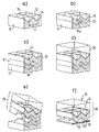
図1Aは例えばp−Siのシリコン基板(半導体基板)10を示しており、またn−Si基板も同様に説明する。Si基板10はその1つの表面に、ピラミッド型窪14のマトリックスと考えられる構造体12と、互いに直接平行して設置される基面とを有しており、そのため表面の上方境界は四角格子に非常に類似している。
FIG. 1A shows a p-Si silicon substrate (semiconductor substrate) 10, for example, and an n-Si substrate will be described in the same manner. The
次に、多孔性シリコン層18(図1B)を生成するために、基板10は既知の方法で処理される。多孔性シリコン層18の上側はSi基板10の構造化表面と同じ形状である。多孔性シリコン層18と基板の間の境界面は同一の形状を有している。
Next, the
次に、基板10をエピタキシャル法によって被覆する。このように、エピタキシャルシリコンの層22が多孔性層18の表面に生成される。原理的には、何れかの既知のエピタキシャル法、特に気相エピタキシー(CVD)、イオン援用エピタキシー、ブラズマ援用エピタキシー、液相エピタキシー及び分子ビームエピタキシーを用いてこの層22を形成することが可能である。
Next, the
図1Cから明らかなように、層22の自由表面も同様に図1Aのシリコン基板及び図1Bの多孔性シリコン層の構造化表面12と同じ形状を有している。層22と多孔性層18の間の境界面も同様に同一形状である。これは、特に多孔性層18が薄い場合に適用される。この図において、層の厚みは「w」で示してある。
As can be seen from FIG. 1C, the free surface of
更に、層22の結晶の向きは、基板10及び基板10から形成された多孔性層18のものと同一である。また、層22は単結晶シリコンで構成されている。
Furthermore, the crystal orientation of the
特に図示していないが、次の段階において、格子電極24を、格子電極24が格子16を形成する線の一部にのみ沿って延びるように層22に当てる。その後層22によって層構造体が形成され、また格子24はガラス層26を備える。このガラス層26は所謂ソル−ゲル処理で生成することができ、これは例えばR.Brendel,A.Gier,M.Menning,H.Schmidt,J.H.Wernerによる出版物「結晶薄膜シリコン太陽電池素子におけるライトトラップのためのソル−ゲル被覆」(Journal of non-crystalline solids,218(1997),391-394)に説明されている。これによると、図1Eに示すように、例えば基板10からガラスカバー円板26を「剥離」するような機械的応力が多孔性層に生じる。このように、多孔性層18から層状構造体の分離が行われ、またこの例では層状構造体はエピタキシャルシリコン層22、格子電極24及びガラスカバー26で構成されている。この点に関して、多孔性層18とエピタキシャル層22の間の境界面で有利に分離が行われ、また機械的な結合に容易に勝るので、この境界面は目的の破断位置として機能する。その後、図1Fに示すように層状構造体28を金属板30に押し当て、このように太陽電池素子を形成する。金属板30は一方では単結晶シリコン層22のピラミッド状の先端32に対する接触部分となり、また他方では反射体としても機能するので、シリコンにまだ吸収されていない光は再び層22を通過して、吸収されることが可能になる。
Although not specifically illustrated, in the next step, the
ちなみに、格子24は金銀線細工であるので、入射光34の反射によって著しく光を損失することはない。
Incidentally, since the grating 24 is made of gold and silver wire, there is no significant loss of light due to the reflection of the
このような光電セルの構造を、図8及び9を参照して更に詳細に説明する。 The structure of such a photoelectric cell will be described in more detail with reference to FIGS.
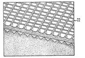
本発明の方法の品質を保証するものとして、まず図2、3、4を参照する。各図は電子顕微鏡の記録を示しており、また図2は図1のエピタキシャルSi層22の上面を、また図3はエピタキシャルSi層22を除去した後に形成される多孔性層の自由表面を示している。また図4はエピタキシャル層22の別の記録であるが、別の視点から示しており、これにより多孔性層18の境界面に問題がないことが分かる。
To assure the quality of the method of the present invention, reference is first made to FIGS. Each figure shows an electron microscope record, FIG. 2 shows the top surface of the
図3の記録はエピタキシャル層22の分離後かつ多孔性層18の残留物を自由表面から取り除く洗浄前の基板18の表面を示している。エッチング及び/または超音波処理による洗浄後、多孔性層18の生成及びエピタキシャルシリコン層22の成長のときと同じ汚れのない基板10の自由表面が現れる。従って、図ICの層22と全く同様に、基板10に新たな多孔性層18を設け、別の層状構造体または半導体層の成長に再使用することができる。
The record of FIG. 3 shows the surface of the
従ってこれは基板10を複数回使用することが可能な第1の方法である。
Therefore, this is the first method that allows the
図5の例では、p−またはp−Si状の基板10を同様に用意し、また構造化多孔性層18もその上に設置する。多孔性層18の最初の自由面の構造は、例えば図1に示す実施例の該当する境界面の断面形に正確に当てはまる。すなわち、19は多孔性層18の最上境界面を表している(つまり基板10から離れた多孔性層18の境界面)。
In the example of FIG. 5, a p- or p-Si-
n−Si及びp−Siの2つの連続する層、すなわち、層22A及び22Bはエピタキシャル法によって基板10、すなわち多孔性層18の構造化表面上で成長する。2つの層22A及び22Bを生成した後、p−Si層22Bの自由表面はまず高さ40まで伸び、境界面19と同一の断面形を有することになる。その後、上方領域の別の多孔性層18A内に形成するために層22Bを処理するが、これは例えば図1の多孔性層18の形状に対応するものである。次にこの過程を複数回繰り返すと、これにより他の層22A’、22B’、22A’’、22B’’、22A’’’、22B’’’等が生成され、また多孔性Si層18A’、18A’’、18A’’’を生成するために上層22B(B’、B’’、B’’’等)の自由表面の処理が毎回行われる。
Two successive layers of n-Si and p-Si, i.e. layers 22A and 22B, are grown on the structured surface of
次に、図5の多重構造体は、各層状構造体22A及び22B(22A’’’’、22B’’’’)、(22A’’’、22B’’’)、...(22A、22Bの順序)を多重構造体から分離させるように分割させる。それぞれn−層及びp−層、すなわち22A、22B、層22A’、22B’、22A’’、22B’’、22A’’’、22B’’’からなる各構造体への図5の層束の分割も、層束を比較的長時間、例えば数時間から数日間エッチング槽に入れておくことで可能となる。多孔性物質のエッチングは実質的にはもっと迅速に行われるが、有用な層22A、22B及び層22A’、22B’等の表面もエッチングされてしまうという問題がある。
Next, the multiple structure of FIG. 5 includes each
別の分離方法では、それぞれの場合のキャリアを次に分離する一組の層の自由表面に結合させることが可能であり、また例えば温度が変化している間に分離を行うことが可能である。洗浄後、所望であれば一組の層に電極を設けることができる。 In another separation method, the carrier in each case can be bound to the free surface of a set of layers that are then separated, and the separation can be performed, for example, while the temperature is changing. . After washing, the electrodes can be provided in a set of layers if desired.
図5に関連する例で説明した数組の層22A、22B等がn−/p−接合を形成するのははっきりと理解される。必要な電極を加えた後、数組の層の一方の表面を、例えば図1に示すようなガラス層を備えるキャリア物質に結合させることが可能である。次に、このような処理を施した数組の層を裏返し、エピタキシャル法によって別の構造体を各下方層22A(22A’、22A’’等)の自由表面に押し当てることができる。場合によっては、構造化多孔性層18を有する基板10を再使用することが可能である。
It is clearly understood that the several sets of
この点については、多孔性Si層は上記のピラミッド形状に限定されるものではないことを強調しておく。実際には、必要に応じて多種多様な構造を選択できる。 In this regard, it is emphasized that the porous Si layer is not limited to the above pyramid shape. In practice, a wide variety of structures can be selected as needed.
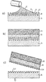
このことも、例えば図6の実施例で明らかになる。つまり、図6Aも多孔性Si層18を有するSi基板10を示している。この場合、多孔性Si層18は、互いに平行して配列され、多孔性シリコン物質のウェブ54でそれぞれ互いに分離している縦溝52で構成される溝状断面50を有している。これらの溝52、または対応するウェブは、例えば機械的平削り、または鋳造工具やならい削りロールを使用して多孔性層18を局所的に粉砕するという所望の方法で形成される。
This also becomes clear, for example, in the embodiment of FIG. That is, FIG. 6A also shows the
次に接着剤56の多孔性層表面への塗布方法の概略を、図6Aに示す。この接着剤56は、所望の材料からなる第2基板58を第1基板10に接着させるもので、図6Bに示す仕上げ構造体が得られる。次に機械的分離処理を行う場合、図6Cに示すように第2基板58が接着層56及びウェブ54の部分(セクション)54Aと共に、第1基板10及びウェブ残留物54Bから分離される。
Next, an outline of a method of applying the adhesive 56 to the surface of the porous layer is shown in FIG. 6A. The adhesive 56 adheres the
製造方法の結果、多孔性層18の結晶の向きが基板10と同一になり、またこの結晶の向きはウェブ54にも含まれることになる。更に、この結晶の向きは全てのウェブ54において同一であり、第2基板58に固定されているセクション54Aにも適合する。次に、セクション54Aを有する基板58を使用し、エピタキシャル法によってセクション54Aを有する自由面上で別の構造体を成長させることができる。このように、単結晶半導体物質が基板58、すなわちウェブ54A上の単結晶シリコン上で生成される。
As a result of the manufacturing method, the crystal orientation of the
次に、第1基板10を再使用して、多孔性層18の残留物を完全に取り除き、図6の方法を再び実行する。この方法の繰り返しは複数回行うことが可能である。
Next, the
図6A〜6Cの実施例において、ならし削りまたは構造化した表面を用いてこの構造体を好適に実現しても、図22、図23で説明する方法により多孔性基板に対する境界面で分離を行う場合、特にこれのみというわけではないが本発明により非構造化多孔性層を使って作業を行うこともできる。 In the embodiment of FIGS. 6A to 6C, even if this structure is preferably realized by using a smoothed or structured surface, separation at the boundary surface with respect to the porous substrate is performed by the method described in FIGS. When doing so, it is possible to work with an unstructured porous layer according to the invention, although this is not the only case.
図7は本発明による方法の別の実施例を示す概略図である。 FIG. 7 is a schematic diagram showing another embodiment of the method according to the present invention.
ここでは、単結晶シリコンの円筒部分を連続的に処理して、多孔性シリコン表面を生成する。このため、円筒棒60の下部をHF槽に軽く浸し、格子電極62と円筒棒60の間に電圧を発生させる。この電圧とHF槽の使用により、電流が発生し、多孔性Si層が生成される。
Here, a cylindrical portion of single crystal silicon is continuously processed to produce a porous silicon surface. For this reason, the lower part of the
円筒棒60を回転させている間、柔軟な基板物質を多孔性Si層の露出面に押し当て、その後例えば硬化剤を吹き付け、更にこれを用いて多孔性Si層を円筒棒60の表面から剥離する。多孔性Si層18は元々は湾曲していたが、基板10による剥離で直線状に伸びているので、所定の部品の製造に利用できる永久応力を有している。この変形例には、帯状構造体、すなわち多数の様々な目的に使用できる帯状多孔性層18を有する帯状基板10を生成できるという利点がある。
While the
例えば、多孔性層18を構造化し、これを用いて上記の何れかの方法を実行することができる。すなわち、まずエピタキシャル法で多孔性Si層18の自由面に半導体層を生成し、これを任意で構造化した後、単結晶物質から成る対応する単一または複数の半導体層を順次生成する。
For example, the
後に柔軟基板を管状に形成し、エピタキシーを行う場合、単結晶Si管が生成する。これは、シリコン管は機械的に非常に安定しており、異質の原子を含んでいないため、エピタキシャル反応装置のシラン供給ラインとして重要となる。また、柔軟性があるため、例えば太陽エネルギーで動作する車両の任意に湾曲したガラス面上に広げられるフォイルの製造にも使用できる。 When the flexible substrate is later formed into a tubular shape and epitaxy is performed, a single crystal Si tube is generated. This is important as a silane supply line for epitaxial reactors because silicon tubes are mechanically very stable and do not contain foreign atoms. It is also flexible and can be used, for example, in the production of foils that are spread on arbitrarily curved glass surfaces of vehicles operating on solar energy.
次に、別の使用方法を詳細に説明する。 Next, another method of use will be described in detail.
A.逆ピラミッドを有する基板の構造化方法:
a)(100)方向付け及び研磨を行ったSiウエハーの1000℃での45分間の酸化(1%トランスLC)。100nm厚さのSiO2層が生成される。
b)網状マスクを使用して、回転させて光食刻法で露出したフォトレジスト。マスクの構成によって、約2μm幅のウェブ上での現像後フォトレジストのみが残り、11×11μm2の自由面がウェブに形成される。
c)約2分間で緩衝HFで酸化物を除去する。フォトレジストが除去される。
d)RCA1及びRCA2洗浄はHFに浸すことで終了する。
e)逆ピラミッド部分を80℃の温度で10分間8%のKOH溶液でエッチングする。エッチング処理の後、サンプルを高純度水で濯いで乾燥させる。酸化ウェブを目に見える程度まで除去する。この異方性エッチング手法により、配向の結晶表面(111)が生じる。面(111)の自由結合部分に安定して水素を染み込ませることができるので、表面でのSiO2の生成を確実に防ぐことができる。従って、次のエピタキシャル過程でも、方法と反応体は酸化物の熱伝導を生じさせないものとして考慮される。
f)他の方法:
f1)KOHでの異方性エッチングにより不規則に配列されたピラミッド(光食刻法ではない)
f2)特殊形状の鋸歯(代表的構造のサイズは100μm)での機械的研削
f3)深くならい削りされた多孔性シリコンを、不均一照明(n−タイプSi)で生成し、後に再び除去する
f4)開始ウエハーは、例えばブロック鋳造材料などの単結晶Siでよい。
A. Method for structuring a substrate with an inverted pyramid:
a) 45 min oxidation (1% trans LC) at 1000 ° C. of (100) oriented and polished Si wafer. A 100 nm thick SiO 2 layer is produced.
b) Photoresist exposed by photoetching using a reticulated mask. Depending on the mask configuration, only the photoresist after development on the web of about 2 μm width remains, and a free surface of 11 × 11 μm 2 is formed on the web.
c) Remove oxide with buffered HF in about 2 minutes. The photoresist is removed.
d) The RCA1 and RCA2 cleaning is completed by immersing in HF.
e) The inverted pyramid portion is etched with 8% KOH solution at a temperature of 80 ° C. for 10 minutes. After the etching process, the sample is rinsed with high purity water and dried. Remove the oxidized web to a visible extent. This anisotropic etching technique produces an oriented crystal surface (111). Since hydrogen can be stably infiltrated into the free bonding portion of the surface (111), generation of SiO 2 on the surface can be surely prevented. Thus, even in the next epitaxial process, the method and reactant are considered not to cause thermal conduction of the oxide.
f) Other methods:
f1) Pyramids randomly arranged by anisotropic etching with KOH (not photoetching)
f2) Mechanical grinding with specially shaped saw blades (typical structure size is 100 μm) f3) Deeply ground porous silicon is generated with non-uniform illumination (n-type Si) and later removed again f4 ) The starting wafer may be single crystal Si, such as a block casting material.
B.構造化ウエハーの表面に多孔性層を生成する方法: B. Method for creating a porous layer on the surface of a structured wafer:
a)ウエハーは50×1018cm-3〜2×1019cm-3の間の受容体濃度でBドープされる。RCA1及びRCA2。HFによる残留酸化物の除去。
b)エッチング装置はEP−A−0536788の図2bに開示されているものに相当する。HFとH2Oとエタノールでの陽極腐食法で多孔性シリコンを生成する。なお、HF:H2O:エタノール=1:1:2(室温で)。基板の構造化側は陰極を向いている。層の多孔性は電流濃度によって調整され、また代表的な電流濃度は1〜100mA/cm2である。
c)低多孔性(約35%)の約150nm厚さの第1多孔性層を生成し、次ぎに高多孔性(50%)の約10μm厚さの第2多孔性層を生成する。
d)構造化多孔性面を有するシリコン円板を乾燥したO2雰囲気の中で30分間400℃酸化させ、エピタキシーの前に不活性気体(N2)で保存する。
a) The wafer is B-doped with a receptor concentration between 50 × 10 18
b) The etching apparatus corresponds to that disclosed in FIG. 2b of EP-A-0536788. Porous silicon is produced by anodic corrosion with HF, H 2 O and ethanol. Note that HF: H 2 O: ethanol = 1: 1: 2 (at room temperature). The structured side of the substrate faces the cathode. The porosity of the layer is adjusted by the current concentration, and a typical current concentration is 1 to 100 mA / cm 2 .
c) Producing a first porous layer of about 150 nm thickness with low porosity (about 35%), followed by a second porous layer of about 10 μm thickness with high porosity (50%).
d) A silicon disc having a structured porous surface is oxidized at 400 ° C. for 30 minutes in a
C.イオン援用沈着のエピタキシャル法:
この処理はS.Oelting,D.Martini,D.Bonnetによる論文「イオン援用沈着による結晶薄膜シリコン太陽電池素子」に詳細に説明されている。図2〜4に示すようにSEMが記録されているサンプルを以下のようにエピタキシー処理する。
a)HFに浸してRCA1及びRCA2洗浄を行う(5%のHFで30秒、その後脱イオン水で濯ぐ)。
b)反応装置に送り込み、400℃〜500℃で気体除去する。
c)残留酸化物を除去するために、10分間850℃に加熱する。
d)5×1017cm-3のGaドープで、(基板ウエハーの巨視的表面垂直線に平行に測定した)10μm厚さのシリコン層が成長した。Gaだまりの温度は670℃であり、また基板温度は700℃である。沈着速度は4μm/hである。高真空(<10-5Pa)で被覆を行う。連続してドーピングした層、特にエピタキシーの間に生成されたpn接合部分は同様に問題なく分離した。
e)他のエピタキシー法
e1)液相エピタキシー(LPE)。LPEは850℃未満の温度で可能であるため興味深い。
e2)非晶質Si(a−Si)の固相結晶化(SPC)。大領域のa−Si沈着を行う沈着プラントは先行技術であるため興味深い。SPCの速度が遅いのが欠点である(再結晶化に5〜10時間)。
e3)Canonによる特許に開示されている気相エピタキシー(CVD)。CVDでは900℃を超える沈着温度が必要となり、多孔性物質が焼結してしまうのが欠点である。機械的分離は困難または不可能である。
e4)プラズマ援用気相エピタキシー(LPCVD)。低温で可能であるため興味深い。
e5)低温(<600℃)で高沈着速度(>1nm/s)が可能であるため、熱線エピタキシー。
e6)迅速であり、また基板及び多孔性Siの低温積載のみ行われるため、非晶質Siのレーザー結晶化。
C. Epitaxial method of ion-assisted deposition:
This process is described in S.A. Oelting, D.C. Martini, D.M. It is described in detail in a paper by Bonnet, “Crystalline Thin Film Silicon Solar Cell Device by Ion-Assisted Deposition”. As shown in FIGS. 2 to 4, the sample on which the SEM is recorded is subjected to an epitaxy process as follows.
a) Dip in HF for RCA1 and RCA2 clean (30% with 5% HF, then rinse with deionized water).
b) Feed into the reactor and remove gas at 400-500 ° C.
c) Heat to 850 ° C. for 10 minutes to remove residual oxide.
d) With a Ga doping of 5 × 10 17 cm −3 , a 10 μm thick silicon layer (measured parallel to the macroscopic surface normal of the substrate wafer) was grown. The temperature of the Ga pool is 670 ° C., and the substrate temperature is 700 ° C. The deposition rate is 4 μm / h. Coating is performed under high vacuum (<10 −5 Pa). The continuously doped layer, in particular the pn junction produced during epitaxy, likewise separated without problems.
e) Other epitaxy methods e1) Liquid phase epitaxy (LPE). LPE is interesting because it is possible at temperatures below 850 ° C.
e2) Solid phase crystallization (SPC) of amorphous Si (a-Si). Deposition plants that perform large-area a-Si deposition are interesting because they are prior art. The disadvantage is the slow SPC rate (5-10 hours for recrystallization).
e3) Vapor phase epitaxy (CVD) as disclosed in the Canon patent. CVD requires a deposition temperature exceeding 900 ° C., and the disadvantage is that the porous material is sintered. Mechanical separation is difficult or impossible.
e4) Plasma assisted vapor phase epitaxy (LPCVD). Interesting because it is possible at low temperatures.
e5) Hot wire epitaxy because a high deposition rate (> 1 nm / s) is possible at low temperatures (<600 ° C.).
e6) Laser crystallization of amorphous Si because it is rapid and only low temperature loading of the substrate and porous Si is performed.
E.分離処理
a)基板ウエハーの多孔性層上の10μm厚さのエピタキシャル層を125°の温度で加熱板上に置く。エピタキシャル層が上になるようにする。
b)加熱したエピタキシャル層の上にグリコールフタル酸塩を載せ、更にその上に2cm×2cm=4cm2のサイズのカバーガラスを置く。この透明高分子は軟化し、ガラス板の重みを受けて流れ、10分後にエピタキシャル層とガラスの間の部分の空気を完全に除去する。冷却後、ガラスは構造化エピタキシャル層に結合される。
b1)グリコールフタル酸塩とは異なる接着剤、例えは光起電性分野で通例となっているプラスチックを使用。
b2)ガラス以外の機械的キャリア、例えばプラスチックフォイルの使用。このような柔軟キャリアは、薄い構造化エピタキシャル層も非常に柔軟であると(弾性太陽電池素子)いうことを利用している。
b3)エピタキシャル層上に…に記載されている。」を「b3)エピタキシャル層上に成形して硬化させることが可能なソル−ゲルガラスの使用。ソル−ゲル手法の詳細については、論文「結晶薄膜においてライトトラップを行うためのソル−ゲル被覆」(R.Brendel et al.,Journal of non-crystalline solids,218(1997),391-394)の「実験」セクションに記載されている。
b4)ガラスへの構造化エピタキシャル層の陽極結合またはSiへのエピタキシャル層の「直接ウエハー結合」。
c)ガラスはエピタキシャル層と共に簡単に分離される。多孔性層は中央部分で一部破損しており、一部は基板に残留しまた別の一部はエピタキシャル層に固着する。2分間の超音波処理により、全ての多孔性Siの残留物は除去される。エピタキシャル層はガラスにしっかりと結合する。剥離の前に超音波処理を実行する場合、ガラスをエピタキシャル層と共に基板から剥離するのに弱い機械的な力が必要である。
E. Separation process a) A 10 μm thick epitaxial layer on a porous layer of a substrate wafer is placed on a heating plate at a temperature of 125 °. The epitaxial layer is on top.
b) A glycol phthalate is placed on the heated epitaxial layer, and a cover glass having a size of 2 cm × 2 cm = 4 cm 2 is further placed thereon. This transparent polymer softens and flows under the weight of the glass plate, and after 10 minutes, completely removes the air between the epitaxial layer and the glass. After cooling, the glass is bonded to the structured epitaxial layer.
b1) Adhesives different from glycol phthalates, eg plastics customary in the photovoltaic field.
b2) Use of mechanical carriers other than glass, such as plastic foil. Such flexible carriers take advantage of the fact that thin structured epitaxial layers are also very flexible (elastic solar cell elements).
b3) on the epitaxial layer. "B3) Use of a sol-gel glass that can be molded and cured on an epitaxial layer. For more information on the sol-gel technique, see the article" Sol-gel coating for light trapping in crystalline thin films "( R. Brendel et al., Journal of non-crystalline solids, 218 (1997), 391-394).
b4) Anodic bonding of structured epitaxial layer to glass or “direct wafer bonding” of epitaxial layer to Si.
c) The glass is easily separated with the epitaxial layer. The porous layer is partially broken at the central portion, part remains on the substrate, and another part adheres to the epitaxial layer. All porous Si residues are removed by sonication for 2 minutes. The epitaxial layer is firmly bonded to the glass. When sonication is performed prior to peeling, a weak mechanical force is required to peel the glass from the substrate along with the epitaxial layer.
機械的分離を行うための別の方法
c1)軽い振動でエピタキシャル層を(例えば)衝撃的に加熱すると、多孔性層に大きな温度勾配が生じ、これによって多孔性層が破砕する。
c2)多孔性層の中空キャビティに液体または気体を充填する。液体または気体は膨張して、エピタキシャル層を破壊する。
c3)エピタキシャル層に大きな機械的圧力を加える。
c4)多孔性層への共振放射結合は導波管として機能するので、多孔性物質に放射が集中する。
Alternative methods for performing mechanical separation c1) When the epitaxial layer is heated (for example) shockously with light vibrations, a large temperature gradient is created in the porous layer, thereby breaking the porous layer.
c2) Filling the hollow cavity of the porous layer with liquid or gas. The liquid or gas expands and destroys the epitaxial layer.
c3) A large mechanical pressure is applied to the epitaxial layer.
c4) Since resonance radiation coupling to the porous layer functions as a waveguide, radiation concentrates on the porous material.
次に、本発明によって実現される半導体部品を説明する。 Next, semiconductor components realized by the present invention will be described.
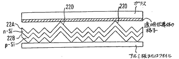
まず、図8及び9は、ここでは太陽電池素子である光電セルを示しており、nタイプSi層から成り図1の層22と同じ形状を有する層状構造体22をコア内に備えている。
First, FIGS. 8 and 9 show a photoelectric cell which is a solar cell element here, and a
アルミニウム板またはフォイル30は層状構造体22の下側に配置され、層状構造体22のピラミッド型先端32に接している。熱処理により、70に示すようにアルミニウム原子は層状構造体22の先端に拡散され、nタイプSiではなくpタイプSiが生成される。つまり、このように光電セルに必要なpn結合が得られる。
The aluminum plate or foil 30 is disposed below the layered
上記の代わりに、層状構造体22を例えば図5に示すように、nタイプSiの第1層22A及びpタイプSiの第2層22Bで構成してもよく、これを破線部分の境界面22Cで示す。電極としても機能する下部反射体の構造は上記と同一である。
Instead of the above, as shown in FIG. 5, for example, the layered
層状構造体22の上には、この例では図9に示すように指状の格子電極24が設けられている。
In this example, finger-
実際的な実施例では、領域は図9に示すものと幾分異なっている。格子電極の各指25は約20μの幅、すなわち層状構造体22の各ピラミッドの幅寸法の約2倍の幅を有している。更に、図に示すように格子指25は5番目の格子ライン毎に設けられているわけではなく、各指間に設けられている露出格子セルの数は非常に多く、その数は例えば1000である。
In a practical embodiment, the area is somewhat different from that shown in FIG. Each
また、例えばインジウム酸化錫などの透明物質から格子電極25を製造することも可能である。格子電極25を、板26の下部の全領域または層状構造体22の上面に設けることもできる。
It is also possible to manufacture the
以下に説明するように、ガラス板の設置を開始する。 As described below, the installation of the glass plate is started.
太陽電池などの場合、この方法でしか大量の太陽光線を薄層に吸収させることができないので、Si層の構造は非常に重要である。既知の方法(平坦または型押しガラスへの直接シリコン沈着)とは対照的に、前側及び後側はここで説明するように自由に手で触れることができる。 In the case of a solar cell or the like, the structure of the Si layer is very important because a large amount of sunlight can be absorbed by the thin layer only by this method. In contrast to known methods (direct silicon deposition on flat or stamped glass), the front and rear sides can be freely touched as described herein.
(例えば1997年1月20日、Appl.Phys.Letters第70巻No.3の390〜392頁に記載されているような)複雑な接触組織は必要ない。エピタキシーで、つまり層22A及び22Bでpnトランジションを生成してあり、例えばガラスなどのキャリア物質上の金属鏡面(例えば上記のアルミニウムシート30)と透明導体(例えばインジウム酸化錫または酸化亜鉛)との間に層状構造体、すなわちワッフルを簡単に固定してあるのであれば、太陽電池素子の製造は非常に単純になる。そのため、触指の蒸着は不要になる。機械的な押圧で十分である。
Complex contact tissue is not necessary (for example, as described on Jan. 20, 1997, Appl. Phys. Letters Vol. 70, No. 3, pages 390-392). Epitaxy, i.e., pn transitions have been created in
太陽電池素子の応用では、構造化基板ウエハーの再使用は重要な特徴である。 In solar cell device applications, the reuse of structured substrate wafers is an important feature.
多孔性層18の厚さを、前回使用した実験値10μmから1μm未満に減少させることが可能である。多孔性層が小さくなると、基板ウエハーの再使用の頻度を上げることができる。
It is possible to reduce the thickness of the
図18及び19は図8及び9と同様の概略図であるが、変形例を示している。 18 and 19 are schematic views similar to FIGS. 8 and 9, but showing a modification.
ここでは、層状構造体の構造は幾分異なる効力を発揮するので、上方層22Aの所定のピラミッド先端22Dが上方を向く。すなわちこの先端は他のピラミッド先端よりも高くなる。この実施例は、基板構造を精巧に選択することによって、層状構造体への接触頻度を格子周期Pから独立して制御する方法を示している。
Here, the structure of the layered structure exhibits somewhat different efficacy, so that the predetermined pyramid tip 22D of the
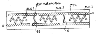
図20は、例えば図8及び9に示す様々な太陽電池素子を直列に接続してモジュールを形成する方法を示している。ここに示すように、上側及び下側電極または導体を互いに電気的に接続するために、バネ80が使用されている。太陽電池素予の三重電圧は、A点とB点との間から得ることができる。
FIG. 20 shows a method of forming a module by connecting various solar cell elements shown in FIGS. 8 and 9 in series, for example. As shown here, a
図10及び11は、放射線検出器の考えられうる実施例を示す概略図である。 10 and 11 are schematic diagrams illustrating possible embodiments of radiation detectors.
ガラス基板に結合されている構造化Siエピタキシャル層22により、閉塞して所定量の気体が充填されている多数の室72が形成される。このように形成されている室は上側ガラス板26によって閉塞されている。放射線がガラスを通過して各室72に入ると、ガスが加熱されて膨張し、層状構造体22で形成されている膜を湾曲させる。この膨張は圧電素子74によって検出することが可能である。検出する放射線の異なる波長に対して検出器の異なる領域を使用する場合、例えば検出する各放射線のみを通過させる上側ガラス板26にフィルターを設ける。
The structured
図10及び11では4つの室72のみ示されている。実際には室の数はこれよりも多い。
10 and 11, only four
図10及び11の構造を圧力センサーに使用することも可能である。ガラスに結合した構造化Siエピタキシャル層に、所定量の気体が充填されている複数のそれぞれ閉塞した室が示されている。外部圧力が変化すると(空気圧または機械的圧力)、室の壁が屈曲する。このような屈曲は、各室でそれぞれ圧電素子によって検出できる。 It is also possible to use the structure of FIGS. 10 and 11 for a pressure sensor. A plurality of closed chambers are shown in which a structured Si epitaxial layer bonded to glass is filled with a predetermined amount of gas. As the external pressure changes (pneumatic or mechanical pressure), the chamber walls bend. Such bending can be detected by a piezoelectric element in each chamber.
層状構造体の別の可能な応用例として、層状構造体の反射面の特殊構造化によって作られる特殊鏡(特別な特徴を有するマイクロミラー)の使用がある。 Another possible application of the layered structure is the use of special mirrors (micromirrors with special characteristics) made by special structuring of the reflective surface of the layered structure.
図12A〜Dは図6と同様の構造体を示しているが、多孔性層の特殊外形形成は行わない。 12A to 12D show a structure similar to that shown in FIG. 6, but the special outer shape of the porous layer is not formed.
具体的には、図12A〜Dは、エピタキシーによって単結晶半導体層が圧着される基板の製造方法を示している。 Specifically, FIGS. 12A to 12D show a method for manufacturing a substrate on which a single crystal semiconductor layer is pressure-bonded by epitaxy.
第一の段階として、半導体物質の基板10、好ましくはシリコンを処理して、平坦な境界面を有する板状の多孔性層を生成する。
As a first step, a
次に、可能であればすでにキャリア58を備えている接着剤56を多孔性層に塗布して、少なくとも接着剤の一部が多孔性層18に浸透するようにする。その後、基板から接着剤を機械的に分離させる。接着剤が機械的に十分な強度を持つ化合物であれば、キャリアは無くてもよい。つまり、接着剤自身がキャリアを形成する。しかし、接着剤は必要に応じてキャリア58で強化させることができる。
Next, if possible, an adhesive 56 already provided with a
可能であればキャリアを有する接着剤の基板10からの分離は、所望の配向性の多孔性半導体物質が分離によって形成される面に浸透するように行う。多孔性物質の被覆を有し、また可能であれはキャリア58を多孔性物質から離れた側に有する接着剤は、後にエピタキシャル法を行うための基板を形成する。
If possible, the adhesive having a carrier is separated from the
通常多孔性物質の残留物を有することになる基板10を、まず洗浄してこれらの残留物を除去する。これで新たに多孔性層が形成され、基板10の再使用が可能になる。
The
図13A〜Hは、所定の部分が単結晶でその他の部分が非晶質である半導体層の製造方法を示している。 13A to 13H show a method for manufacturing a semiconductor layer in which a predetermined portion is a single crystal and the other portions are amorphous.
図13Aによれば、例えばSiなどの単結晶または多結晶半導体物質から成る平坦基板を初めに設ける。 According to FIG. 13A, a flat substrate made of a monocrystalline or polycrystalline semiconductor material such as Si is first provided.
図13Bは、溝または穴、あるいは研削またはエッチングによる所望のパターンを設けることで基板の一方の面を構造化し、構造体深さhを得ることを非常に簡略に示している。 FIG. 13B very simply shows that one side of the substrate is structured to provide a structure depth h by providing grooves or holes or a desired pattern by grinding or etching.
図13Cによれば、厚さWPSの多孔性層を、例えはHFでの陽極腐食法などの既知の方法で生成する。 According to FIG. 13C, a porous layer having a thickness of WPS is produced by known methods such as anodic corrosion with HF.
その後、例えばソル−ゲルガラスなどの接着剤を構造体の構造化表面に塗布し、その全てまたは一部を多孔性層に浸透させる。これにより、図13Dに示すように接着剤が浸透した多孔性層18が形成される。
Thereafter, an adhesive, such as sol-gel glass, is applied to the structured surface of the structure and all or part of it penetrates into the porous layer. Thereby, as shown in FIG. 13D, the
その後、図13Eに示すように基板から接着剤を機械的に分離し、また接着剤56が浸透している多孔性層の一部は接着剤に結合する。そして適切な表面処理(多孔性層の残留物の除去及び任意での新たな構造化)の後、基板10を使用することが可能になる。
Thereafter, as shown in FIG. 13E, the adhesive is mechanically separated from the substrate, and a part of the porous layer into which the adhesive 56 penetrates is bonded to the adhesive. And after an appropriate surface treatment (removal of porous layer residues and optional new structuring), the
(可能であればキャリアを有する)接着剤及び接着剤が浸透した多孔性加工物質から成る第2基板に例えば研磨などの処理を施し、図13Fに示すように確定した結晶配向性で一部に多孔性物質を含むが、別の部分では多孔性物質を含まない層状構造体を形成する。 A second substrate made of an adhesive (possibly with a carrier) and a porous processing material into which the adhesive has penetrated is subjected to a process such as polishing, and partially with a determined crystal orientation as shown in FIG. 13F. A layered structure is formed that includes a porous material but does not include a porous material in another portion.
その後、図13Gに示すように、13Fの段階で表面78の全域に非晶質層76を沈着させる。
Thereafter, as shown in FIG. 13G, an
その後、図13Hに示すように、例えば熱処理を行って、非晶質物質の固相結晶化が発生し、接着剤内の多孔性物質が確定した配向性の核形成シードが得られる。多孔性層が無い部分では物質は非晶質のままである。図13Bによると、これに対応する位置は基板10の構造化を行っている間に窪み14が形成された位置である。図13Hに示す構造体は、フラットスクリーンなどの製品を製造する開始点を形成する。つまり、非晶質部分で発光するよう図13H製品を構造化しつつ、非晶質部分で発光状態を制御する単結晶部分で制御トランジスタを形成することが可能になる。
Thereafter, as shown in FIG. 13H, for example, heat treatment is performed, solid-phase crystallization of the amorphous material occurs, and an oriented nucleation seed in which the porous material in the adhesive is determined is obtained. The material remains amorphous where there is no porous layer. According to FIG. 13B, the corresponding position is the position where the recess 14 was formed while the
本発明による別の興味深い可能性は、上記のようにまず表面近くで基板を多孔性にし、結晶Si層をエピタキシーによって多孔性層上に設けるのではなく、急速溶解とそれに続く凝固によって多孔性層の一部を上記とは異なる方法で単結晶多孔性層に変換するものである。つまり、まず多孔性層の最上層を少なくとも局所的に融解させ、その後再び凝固させる。 Another interesting possibility according to the invention is that, as described above, the substrate is first made porous near the surface and the crystalline Si layer is not deposited on the porous layer by epitaxy, but by rapid dissolution followed by solidification. Is converted into a single crystal porous layer by a method different from the above. That is, the top layer of the porous layer is first melted at least locally and then solidified again.
このことは多孔性基板のエピタキシーの一種としても理解されうる。しかし、エピタキシーの物質は多孔性層自身から生じている。多孔性層の溶融とその後の凝固によって単結晶非多孔性層を生成した後は、凝固層を一度基板から分離させるか、あるいは凝固層上で層状構造体を成長させてから凝固層を基板から分離させることができる。 This can also be understood as a type of porous substrate epitaxy. However, the epitaxy material originates from the porous layer itself. After forming the single crystal non-porous layer by melting the porous layer and subsequent solidification, the solidified layer is separated from the substrate once or the layered structure is grown on the solidified layer and then the solidified layer is removed from the substrate. Can be separated.
多孔性層内、またはその多孔性層との境界面に機械的歪みを生成させることにより、あるいは図22、図23を参照して説明した方法を用いて、目的の破砕位置として多孔性層を有する層を使って予め分離を行う。 By generating mechanical strain in the porous layer or at the interface with the porous layer, or by using the method described with reference to FIGS. 22 and 23, the porous layer can be used as the target crushing position. Separation is performed in advance using a layer having the same.
好適には、エキシマーまたは銅蒸気レーザーからのレーザー光パルスを放射して溶融を行う。これは例えば1995年10月26日Electronics Letter第31巻、第22号、1956〜1957頁におけるIshihara及びM.Matsumuraによる出版物「ガラス質基板上のSi膜の巨大粒の成長」に記載されている方法に従って行うことができる。 Preferably, melting is performed by emitting laser light pulses from an excimer or copper vapor laser. This is described, for example, in Ishihara and M. et al., October 26, 1995, Electronic Letters Vol. 31, No. 22, pp. 1956-1957. It can be carried out according to the method described in the publication by Matsumura “Growth of giant grains of Si films on glassy substrates”.
この出版物に記載の方法と異なっている点は、多孔性シリコンを単結晶Siに変化させることである。短い光パルスは同様に可能であり、このように表面に近い部分のみ溶融でき、下部に存在する多孔性物質を変化させないので、長時間の放射に比較して有利である。発生する熱勾配により結晶層が裂けてしまうという技術的問題点もある。この問題は、多孔性Siを適切に調整するか、あるいは層の生成と分離を一度に行うことで防ぐことができ、これは本発明によれば可能である。 The difference from the method described in this publication is that the porous silicon is changed to single crystal Si. Short light pulses are possible as well, and only the portion close to the surface can be melted in this way, and the porous material existing underneath is not changed, which is advantageous compared to long-term radiation. There is also a technical problem that the crystal layer is torn due to the generated thermal gradient. This problem can be prevented by appropriately adjusting the porous Si or by generating and separating layers at once, which is possible according to the invention.
レーザー処理に代わる方法としては、急速加熱の一方法としてゾーンドローイングが考えられる。この方法において、多孔性層は直線的に束になった電子ビームまたは光ビームの下にガイドされるので、部分的結晶層が生じる。これに対応する方法は、太陽エネルギー物質及び太陽電池素子41/42(1996),119〜126頁におけるM.Pauli,T.Reindl,W.Kr hler,F.Homberg and J.Mllerによる「低コスト薄膜太陽電池素子に適したグラファイト基板上の多結晶シリコン層の新規製造方法」という標題の出版物に記載されており、この論文はElsevier Science B.Vによって出版されている。 As an alternative to laser treatment, zone drawing can be considered as one method of rapid heating. In this way, the porous layer is guided under a linear bundle of electron or light beams, resulting in a partially crystalline layer. A corresponding method is described in the solar energy material and solar cell element 41/42 (1996), pages 119-126. Pauli, T .; Reindl, W.M. Kr hler, F.M. Homberg and J.H. Mller, described in a publication entitled “A Novel Method for Fabricating a Polycrystalline Silicon Layer on a Graphite Substrate Suitable for Low-Cost Thin-Film Solar Cell Devices”, which was published by Elsevier Science B. Published by V.
次に、別の観点から本発明を説明する。 Next, the present invention will be described from another viewpoint.
以下に、効率よくライトトラップを行う極薄シリコン層を生成するための多孔シリコンの加工(Ψ加工)について説明する。このために、構造化単結晶シリコン基板の多孔性面上でシリコン層をエピタキシャルに成長させる。機械的応力により多孔性層が破壊されるので、基板からエピタキシャル層が分離する。X線回折分析により、Wf=5.8μm厚さのシリコン層は単結晶である。ワッフル形状の層であり、これらの層がガラスに固定されている場合、反射率測定値及び光線追跡シミュレーションによりjSC*の最大短絡電流が36.5mA/cm2であると予測される。Wf=2〜3μmの膜厚さに対しては、輸送シミュレーションで効率η=16〜19%であることが予測される。 Hereinafter, processing of porous silicon (Ψ processing) for generating an ultrathin silicon layer that efficiently performs light trapping will be described. For this purpose, a silicon layer is grown epitaxially on the porous surface of the structured single crystal silicon substrate. Since the porous layer is broken by the mechanical stress, the epitaxial layer is separated from the substrate. According to X-ray diffraction analysis, the silicon layer with a thickness of Wf = 5.8 μm is a single crystal. If the layers are waffle-shaped, and these layers are fixed to glass, the maximum short-circuit current of jSC * is predicted to be 36.5 mA / cm 2 by reflectance measurements and ray tracing simulation. For a film thickness of Wf = 2 to 3 μm, it is predicted that the efficiency η = 16 to 19% in the transport simulation.
1.序論
結晶シリコンの薄層太陽電池素子は、例えば[1]の文献から既知である。この文献及び次に挙げられる文書には角括弧内に記された番号が付され、要約の目的で一覧の説明末尾部分に記載されている。結晶シリコンの薄膜太陽電池素子には、本質的に3つの必要事項がある。
1. Introduction Crystalline silicon thin-layer solar cell elements are known, for example, from the literature [1]. This document and the following documents are numbered in square brackets and are listed at the end of the list for summary purposes. There are essentially three requirements for crystalline silicon thin film solar cell elements.
(i)廉価な基板上での高品質及び大粒度の結晶シリコン層の成長、(ii)結晶シリコンでの本質的に弱く略赤外線の吸収を補正するためのライトトラップ法の実現、(iii)粒境界及び表面の効果的な皮膜保護。 (I) Growth of high quality and large grain crystalline silicon layers on inexpensive substrates; (ii) Realization of a light trap method to correct intrinsically weak and nearly infrared absorption in crystalline silicon; (iii) Effective film protection on grain boundaries and surfaces.
フロートガラス上の構造化された単結晶シリコン層により、次の3つの必要事項を満たすことができる。(i)単結晶物質は高容量品質を有し、またフロートガラスは廉価な基板である。(ii)例えばピラミッド型層構造体[4]などの革新的な層構造体[2〜4]により効率よくライトトラップを行うことができる。(iii)単結晶構造体により粒境界の組み換えを防止でき、また低温度[5]で効果的な表面被膜保護を可能にする。このような薄い構造化単結晶シリコン層の製造は、今までのところ文献に記載されていない。 A structured single crystal silicon layer on float glass can meet the following three requirements: (I) Single crystal material has high capacity quality, and float glass is an inexpensive substrate. (Ii) Light traps can be efficiently performed by innovative layer structures [2-4] such as pyramid-type layer structures [4]. (Iii) The single crystal structure can prevent recombination of grain boundaries and enables effective surface coating protection at low temperature [5]. The production of such a thin structured single crystal silicon layer has not been described so far in the literature.
以下に、フロートガラス上に構造化単結晶薄層を製造するための多孔シリコンの新規な処理について説明する。この点で、このような層のライトトラップ作用を試験的に調査する。考えられうる新規層構造体の能力を理論的に分析する。 In the following, a novel treatment of porous silicon for producing a structured single crystal thin layer on float glass will be described. In this respect, the light trapping effect of such a layer is investigated experimentally. Theoretically analyze the potential of the new layer structure that can be considered.
2.多孔シリコンの処理
多孔性シリコンのエピタキシーは、絶縁基板[6]上へのこの単結晶シリコン層の生成で詳細に調査した。この処理において、エピタキシャル層は温度T>1000℃でのCVD処理により、多孔性表面を有する平坦な単結晶シリコンウエハー上で成長する。次に、エピタキシャル層は、ウエハー結合により絶縁体上に圧着される。そして機械的研削で、基板ウエハーが除去される。残留する多孔性層のケミカルエッチングで処理は完了する。ライトトラッブ特性の欠如、結合処理、基板ウエハーの消耗があるため、コストの面からもこの技術を光起電力技術には使用できない。
2. Porous silicon treatment The epitaxy of porous silicon was investigated in detail in the production of this single crystal silicon layer on an insulating substrate [6]. In this process, the epitaxial layer is grown on a flat single crystal silicon wafer having a porous surface by a CVD process at a temperature T> 1000 ° C. The epitaxial layer is then crimped onto the insulator by wafer bonding. Then, the substrate wafer is removed by mechanical grinding. The process is completed by chemical etching of the remaining porous layer. Due to the lack of light trap characteristics, bonding processing, and substrate wafer consumption, this technology cannot be used for photovoltaic technology because of its cost.
これとは対照的に、以下に挙げる処理はライトトラップを容易にし、結合処理を行わず、また基板ウエハーを消耗させることはないので、光起電力技術に使用できる。図1A〜Fは、ガラス上に構造化単結晶シリコン層を生成する処理段階を示している。 In contrast, the processes listed below can be used in photovoltaic technology because they facilitate light trapping, do not perform the bonding process, and do not consume the substrate wafer. 1A-F show processing steps for producing a structured single crystal silicon layer on glass.
a)単結晶シリコン基板ウエハーは、何れかの種類のエッチングまたは機械的研削によって表面構造体を受容する。この点で、構造体を、図1Aの周期性pの通常の逆ピラミッドよりも更に複雑にさせることができる。
b)基板の表面を、厚さWPSの多孔性シリコン層(多孔性Si層、PSL)に変化させる。PSL内のシリコンの配向性は、基板の配向性に関する情報を伝える。
c)シリコンはPSL上に順次エピタキシャルに成長する。PLSの内面でのシリコン原子の表面移動性は850℃を超える温度[7]での焼結処理に至るので、低温エピタキシャル技術は有益である。
この時点では、エピタキシャル層の外面に自由に触れることができる。約850℃未満の温度で行われる各処理によって、セルのエミッタを形成することができる。エピタキシャルエミッタの他に、逆転層や異質接合エミッタが可能である。表面の被膜保護と格子形成については、例えば[5,8,9]に記載されている革新的技術を使用するとよい。
d)上に重なる基板(例えばガラス)は、透明な接着剤で前面に固定される。上に重なる基板及び接着剤の温度安定性によって、その後に行われる全ての処理段階の最高処理温度が決まる。
e)基板からセルを分離させるために、基板シリコンと比較して低いPSLの機械的強度を使用する。複数の様々な処理方法が可能である。例えば、大きな内部応力を生じさせる加熱、膨張する液体または気体の穴の中への充填、圧縮または引っ張り応力によるPSLの引っ張り、あるいは超音波処理が挙げられる。どの場合も、PSLはシリコンの穿孔(Psi)として機能するので、(と呼ぶ。
f)セルの後側は、表面被覆保護及び反射体の形成のために触れることができる。オフセット反射体も、少数電荷キャリアの低組み換えに耐える点接触を形成することができる。
a) The single crystal silicon substrate wafer receives the surface structure by any kind of etching or mechanical grinding. In this regard, the structure can be made more complex than the normal inverted pyramid with periodicity p in FIG. 1A.
b) The surface of the substrate is changed to a porous silicon layer (porous Si layer, PSL) having a thickness of WPS. The orientation of the silicon within the PSL conveys information regarding the orientation of the substrate.
c) Silicon grows epitaxially sequentially on the PSL. Since the surface mobility of silicon atoms on the inner surface of the PLS leads to a sintering process at a temperature [7] exceeding 850 ° C., the low temperature epitaxial technique is beneficial.
At this point, the outer surface of the epitaxial layer can be freely touched. Each treatment performed at a temperature below about 850 ° C. can form the emitter of the cell. In addition to epitaxial emitters, inversion layers and heterojunction emitters are possible. For surface coating protection and grid formation, for example, the innovative techniques described in [5, 8, 9] may be used.
d) The overlying substrate (eg glass) is fixed to the front surface with a transparent adhesive. The temperature stability of the overlying substrate and adhesive determines the maximum processing temperature for all subsequent processing steps.
e) Use low PSL mechanical strength compared to substrate silicon to separate the cells from the substrate. A plurality of different processing methods are possible. For example, heating to create large internal stresses, filling in expanding liquid or gas holes, pulling PSL with compressive or tensile stress, or sonication. In any case, PSL functions as a silicon perforation (Psi) and is therefore called (.
f) The back side of the cell can be touched for surface coating protection and reflector formation. Offset reflectors can also form point contacts that withstand low recombination of minority charge carriers.
後及び前面の自由可触性は、シリコンを絶縁基板に直接沈着させる処理に勝る処理φに固有の利点である。 The rear and front free accessibility is an inherent advantage of the process φ over the process of depositing silicon directly on the insulating substrate.
PSLの形成により、結晶表面が巨視的セル表面に対して角度αを成すよう構造化されている基板ウエハーの厚さWPS/Cos(α)が消耗してしまう。全ての残留多孔性シリコンを除去した後、WPS/p<<1と仮定すると、基板は基の表面形態(図1A)を保持する。それ以外では、図1Eに示すように端面及び先端を曲率半径WPS/pで丸める。従って基板は、基板の新たな構造化が必要になるまで、十分に小さな比率WPS/pで複数回再使用することが可能である。 The formation of PSL consumes the thickness WPS / Cos (α) of the substrate wafer that is structured such that the crystal surface forms an angle α with the macroscopic cell surface. After removing all residual porous silicon, assuming WPS / p << 1, the substrate retains the underlying surface morphology (FIG. 1A). Otherwise, as shown in FIG. 1E, the end face and the tip are rounded with a radius of curvature WPS / p. Thus, the substrate can be reused multiple times at a sufficiently small ratio WPS / p until a new structuring of the substrate is required.
3.試験的調査
3.1 サンプルの用意
ホウ素で1019cm-3にドープし、(100)の方向を配向され、4インチ直径を有するp+タイプの単結晶シリコンウエハーに、光食刻法及びKOHを使った異方性エッチングにより、周期性p=13μmで逆ピラミッド構造を与える。希釈HFでの陽極腐食法によって、約2分でWPS=6μm厚さの多孔性シリコン層が生成される。エピタキシーの前に、サンプルを約10分間850℃に加熱して、PSL表面から自然発生した酸化物を除去する。WPS=5,8μm厚さのGaドーピングしたエピタキシャルシリコン層は、700℃でのイオン援用沈着技術(IAD)[10]によって成長する。成長速度は、平面で4μm/hになる。透明なポリ(エチレン−フタル塩酸)により、2×2cm2寸法のガラス表面がエピタキシャル層に固定される。約2分間の超音波処理はPSL層を不安定にし、化学エッチングを行わなくてもエピタキシャル層の機械的な除去を用意にする。また、超音波処理を実行することなく、エピタキシャル層及び基板を互いに分離させることも可能である。
3. Experimental Investigation 3.1 Sample Preparation A p + type single crystal silicon wafer doped with boron to 10 19 cm −3 and oriented in (100) direction and having a 4 inch diameter is subjected to photo-etching and KOH. The anisotropic etching used gives an inverted pyramid structure with periodicity p = 13 μm. The anodic corrosion method with diluted HF produces a porous silicon layer with a thickness of WPS = 6 μm in about 2 minutes. Prior to epitaxy, the sample is heated to 850 ° C. for about 10 minutes to remove the naturally occurring oxide from the PSL surface. The Ga doped epitaxial silicon layer with WPS = 5,8 μm thickness is grown by ion assisted deposition technique (IAD) [10] at 700 ° C. The growth rate is 4 μm / h on a plane. Transparent poly (ethylene-phthalic hydrochloric acid) fixes the 2 × 2 cm 2 size glass surface to the epitaxial layer. Sonication for about 2 minutes destabilizes the PSL layer and provides for mechanical removal of the epitaxial layer without chemical etching. It is also possible to separate the epitaxial layer and the substrate from each other without performing ultrasonic treatment.
3.2 サンプルの特徴付け
図2及び4は、φ処理で生成された自由定常シリコンワッフル構造体を走査電子顕微鏡で記録したものを示している。超音波処理は別として、走査電子顕微鏡を使った調査の前には洗浄は行わない。図2の透視平面図は、基板ウエハーの元の表面構造のコピーである規則的逆ピラミッドを示している。図4はワッフル構造の断面を斜めに示している。ピラミッドの先端は下側を向いている。亀裂は見られない。ピラミッド型の結晶面に垂直な層厚さは、Wf=5.8μmである。上面側には図2及び4の目に見えない窪みがあり、その窪みの深さ及び直径はそれぞれ0.1μm未満である、これは一種の極小粗さを表している。これらの窪みは、非構造化基板シリコン上で成長する平坦なエピタキシャル層でも生じるので、IAD技術に対応する。
3.2 Characterization of the Samples FIGS. 2 and 4 show a free-standing silicon waffle structure produced by the φ process recorded with a scanning electron microscope. Aside from sonication, no cleaning is performed prior to investigation using a scanning electron microscope. The perspective plan view of FIG. 2 shows a regular inverted pyramid that is a copy of the original surface structure of the substrate wafer. FIG. 4 shows an oblique cross section of the waffle structure. The tip of the pyramid faces downward. There are no cracks. The layer thickness perpendicular to the pyramid crystal plane is Wf = 5.8 μm. There are invisible depressions in FIGS. 2 and 4 on the upper surface side, and the depth and diameter of the depressions are each less than 0.1 μm, which represents a kind of minimal roughness. These cavities also occur in flat epitaxial layers grown on unstructured substrate silicon and therefore correspond to IAD technology.
高抵抗率の非構造化単結晶基板に沈着した層の穴を測定すると、2×1017cm-3の電気的に活性化している微量の添加物物質Gaの濃度と186cm2/Vsの穴の移動性が分かる。 Measuring the hole in the layer deposited on the unstructured single crystal substrate with high resistivity, the concentration of 2 × 10 17 cm −3 of the electrically active trace substance additive Ga and the hole of 186 cm 2 / Vs You can see the mobility.
図14は、単結晶シリコン基板のスペクトルと比較したガラス上のシリコンワッフルのCuKαX線回折スペクトルを示している。強度は対数尺で示している。ピークは全て同じ角度で生じる。従って、シリコンワッフル構造体は単結晶であり、基板ウエハーと同じ配向性を有している。大きな(400)ピークのみシリコンに基づいている。その他のピークは全て2段階以上小さく、X線装置で生じたものである。エピタキシャル層のバッタグラウンド強度は、非晶質ガラス基板によって生じる。その結果、IAD技術[10]により、多孔性基板上でのエピタキシャルな成長が可能となる。 FIG. 14 shows the CuKα X-ray diffraction spectrum of a silicon waffle on glass compared to the spectrum of a single crystal silicon substrate. Intensity is shown on a logarithmic scale. All peaks occur at the same angle. Therefore, the silicon waffle structure is a single crystal and has the same orientation as the substrate wafer. Only the large (400) peak is based on silicon. All other peaks are smaller by two or more steps and are produced by the X-ray apparatus. The background strength of the epitaxial layer is generated by the amorphous glass substrate. As a result, the IAD technique [10] enables epitaxial growth on the porous substrate.
基板少数電荷キャリアの寿命は、太陽電池素子の何れかの臨界物質パラメータである。基板の寿命を評価するために、表面に充分に皮膜保護を施さなければならない。従って、自由定常シリコンワッフルは、1000℃の温度で両面で酸化される。表面の組み換え中心から少数電荷キャリアを忌避するために、コロナ放電室[11]によって表面を帯電させる。 The lifetime of substrate minority charge carriers is a critical material parameter of any solar cell element. In order to evaluate the lifetime of the substrate, the surface must be sufficiently protected. Thus, the free stationary silicon waffle is oxidized on both sides at a temperature of 1000 ° C. To repel minority charge carriers from the surface recombination centers, the surface is charged by a corona discharge chamber [11].
図15は、20nsの光パルスで励振した後のマイクロ波反射率の配置を示している。最適感度[12]を得るために、サンプルは4分の1マイクロ波波長によって金属反射体よりも上に配置されている。急激な下降は厳密には単指数ではない。しかし、これにより寿命がτ=0.27μs±0.08μsで推定される。時間t>0.6μsに対する緩慢な下降は、平坦レベルでの電荷キャリアの軟化(解放)によって生じる。電子の移動性は測定されなかった。しかし、測定した穴の移動性μ=186cm2/Vsを考慮すると、少数電荷キャリア拡散長さL>11μmが電子の移動性の下限として求められ、またこれは膜厚さWf=5.8μmよりも大きい。 FIG. 15 shows the arrangement of the microwave reflectivity after excitation with a 20 ns light pulse. To obtain optimum sensitivity [12], the sample is placed above the metal reflector by a quarter microwave wavelength. Strict decline is not strictly a single index. However, the lifetime is estimated at τ = 0.27 μs ± 0.08 μs. The slow decline for time t> 0.6 μs is caused by softening (release) of charge carriers at a flat level. Electron mobility was not measured. However, considering the measured hole mobility μ = 186 cm 2 / Vs, the minority charge carrier diffusion length L> 11 μm is obtained as the lower limit of the electron mobility, and this is from the film thickness Wf = 5.8 μm. Is also big.
薄膜セルの場合、ライトトラップは重要である。残念ながら、図1Fの概略図に示すようにサンプルの後ろにアルミニウム鏡を備える粘着結合したワッフル構造体の理想的な作用は、サンプルに接触しないで測定することはできない。従って、サンプルの短電流電位を、測定した半球反射率との比較とプログラムSUNRAYS[13]による光線追跡シミュレーションとから推定した。オフセット反射体はA1で光損失が実質的に減少することが分かった。 For thin film cells, light traps are important. Unfortunately, the ideal action of an adhesively bonded waffle structure with an aluminum mirror behind the sample as shown in the schematic diagram of FIG. 1F cannot be measured without contacting the sample. Therefore, the short current potential of the sample was estimated from a comparison with the measured hemispheric reflectivity and a ray tracing simulation with the program SUNRAYS [13]. It has been found that the offset reflector substantially reduces optical loss at A1.
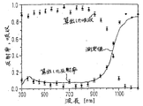
図16は測定(連続線)及び算出(円)した半球反射率を示す。光線追跡シミュレーションによって、光学パラメータを適合させずに測定値をほぼ再生することができる。測定値とシミュレーションとの間の小さな偏差は、シミュレーション[2]には考慮しなかったピラミッド型結晶面の微少粗さによって質的に説明される。SUNRAYSは、1000W/m2のAM1.5Gスペクトルを有する放射線の構造周期p=13μmを有するWf=5.8μm厚さワッフルの疑似吸収(三角)から、最大短絡電流jSC*=36.5mA/cm2±0.5mA/cm2を計算する。モンテカルロシミュレーションの統計の結果、誤差帯が生じる。 FIG. 16 shows the measured hemispherical reflectance (continuous line) and calculated (circle). The ray tracing simulation can almost reproduce the measured value without adapting the optical parameters. The small deviation between the measured value and the simulation is qualitatively explained by the microroughness of the pyramidal crystal plane that was not considered in the simulation [2]. SUNRAYS has a maximum short-circuit current jSC * = 36.5 mA / cm, from a pseudo absorption (triangle) of Wf = 5.8 μm thickness waffle with a structural period p = 13 μm of radiation having an AM1.5G spectrum of 1000 W / m 2. 2 Calculate ± 0.5 mA / cm 2 . As a result of the Monte Carlo simulation statistics, an error band occurs.
4.考えられる効率
図2及び4に示す形状を有する結晶シリコン層の考えられる効率を、理論モデリングで調査する。光学モデルでは、蒸気のSUNRAYSによる光線追跡を実行する。小数電荷キャリアの生成速度をシリコン層において空間的に均一になるようにし、またこれをjSC*及びセル容積から計算する。光学モデルに加えて、電子伝達のモデルも必要である。シリコンワッフルにおける複雑な三次元電荷キャリア拡散を、ピラミッド型結晶面に垂直な純一次元伝達で概算する。セルの効率は、小数電荷キャリア拡散長さL及び(鏡面組み換え速度SRV)Sによって異なる。固定のL及びS[14]の考えられうる効率を正しく推定するために、セル厚さWfを最適化することは非常に重要である。従って、シミュレーションによって、理想的なセル効率の膜厚さWが変化する。シリコンセルは1019cm-3及び0.5μm厚さにpドープしたエミッタを備え、1018cm-3にBドープした基部を有する。W<1μm厚さの場合、基部及びエミッタの厚さは同一である。自由パラメータの数を減らすために、拡散長さL及び表面組み換え速度Sは基部及びエミッタに対して同等と見なされる。空間電荷ゾーンにおける組み替えを[15]で説明する。cシリコンのバンドギャップ縮小の移動性値及びパラメータは、文書[14]から引用する。
4). Possible efficiency The possible efficiency of the crystalline silicon layer having the shape shown in FIGS. 2 and 4 is investigated by theoretical modeling. In the optical model, ray tracing by vapor SUNRAYS is performed. The rate of generation of fractional charge carriers is made spatially uniform in the silicon layer and is calculated from jSC * and the cell volume. In addition to the optical model, an electron transfer model is also required. The complex three-dimensional charge carrier diffusion in a silicon waffle is approximated by pure one-dimensional transmission perpendicular to the pyramidal crystal plane. The efficiency of the cell depends on the fractional charge carrier diffusion length L and (mirror recombination rate SRV) S. It is very important to optimize the cell thickness Wf in order to correctly estimate the possible efficiency of the fixed L and S [14]. Therefore, the film thickness W with an ideal cell efficiency varies depending on the simulation. The silicon cell has an emitter that is p-doped to 10 19 cm −3 and 0.5 μm thickness and has a base that is B-doped to 10 18 cm −3 . For W <1 μm thickness, the base and emitter thickness are the same. In order to reduce the number of free parameters, the diffusion length L and the surface recombination rate S are considered equivalent for the base and emitter. Recombination in the space charge zone is described in [15]. The mobility values and parameters for band gap reduction of c-silicon are taken from document [14].
図17は、広範囲のパラメータS及びLに対する最適セル厚さ(破線)の効率(連続線)を表している。拡散長さL=11μmのとき、16〜19%のエネルギー変換効率が2〜3μm(点)の理想的七ル厚さの表面組み換え速度Sに基づいて求められる。ガラス上の2μm厚さ結晶シリコン太陽電池素子に対しては、SRVS=104cm/sに相当する16%の効率で充分である。Wf=2μm薄層の沈着には、現在使用されているIAD技術で50分を要する。 FIG. 17 represents the efficiency (continuous line) of the optimum cell thickness (dashed line) for a wide range of parameters S and L. When the diffusion length L = 11 μm, the energy conversion efficiency of 16 to 19% is obtained based on the surface recombination speed S of an ideal seven-thickness of 2 to 3 μm (point). For a 2 μm thick crystalline silicon solar cell element on glass, an efficiency of 16% corresponding to SRVS = 104 cm / s is sufficient. The deposition of a thin layer of Wf = 2 μm takes 50 minutes with the currently used IAD technology.
穿孔シリコンの新たな処理(φ処理)を説明した。構造化単結晶シリコン基板上でエピタキシーを行い、基板からエピタキシャル層を機械的に分離させると、何れかの種類のガラス上に極薄単結晶構造化シリコン層が形成される。反射能力の測定値により、最大短絡電流jSC*=36.5mA/cm2に対応する光学吸収が明らかになった。理論的には物質の品質は、Wf=2〜3μmの範囲の理想的セル厚さでの16〜19%効率に対しては充分である。 A new treatment (φ treatment) for perforated silicon has been described. When epitaxy is performed on a structured single crystal silicon substrate and the epitaxial layer is mechanically separated from the substrate, an ultrathin single crystal structured silicon layer is formed on any type of glass. The measured value of the reflection ability revealed an optical absorption corresponding to the maximum short-circuit current jSC * = 36.5 mA / cm 2 . Theoretically, the quality of the material is sufficient for 16-19% efficiency with an ideal cell thickness in the range of Wf = 2-3 μm.
他の実現可能なφ処理としては、物質の消耗を減らすために多孔性層の厚さをWPS<1μmにし、基板ウエハーの度重なる再使用を可能にすることが挙げられる。沈着速度の上昇も同様に可能である。100cm2寸法の極薄層は問題なく生成できる。 Another possible φ treatment is to reduce the material consumption by setting the thickness of the porous layer to WPS <1 μm to allow repeated reuse of the substrate wafer. An increase in deposition rate is possible as well. An ultra-thin layer with a size of 100 cm 2 can be produced without problems.
また、本発明の特に好適な実施例を以下に説明するが、これは太陽電池素子の製造に関連している。ここに説明する方法は光電セルに限定されるものではないが、一般的な製造過程として理解されるべきである。本実施例の動機付けは、太陽電池素子の直列接続により、高電圧及び小電流で太陽電池素子モデルから電力を得ることが可能ということにある。電流が小さいとオーム損失が減少する。太陽電池素子の前及び後側の触指も、オーム損失を減らすようになっている。従って、適切な統台直列接続により、接触跡を消すことができる。 Also, a particularly preferred embodiment of the present invention will be described below, which relates to the manufacture of solar cell elements. The method described here is not limited to photocells, but should be understood as a general manufacturing process. The motivation of the present embodiment is that electric power can be obtained from the solar cell element model with high voltage and small current by connecting the solar cell elements in series. Small current reduces ohm loss. The front and rear tentacles of the solar cell element are also designed to reduce ohmic loss. Therefore, the contact mark can be erased by appropriate series connection of the bases.
このような直列接続は、シャドーマスクを使用することで実現される。ここでは、太陽電池素子の直列接続はすでに層の製造の中で、つまり(所定の位置のみで)層が選択的に成長している際に行われている。層の成長の位置はシャドーマスクで制御される。シャドーマスクは引っ張られた状態のワイヤーで好適に実現される。 Such series connection is realized by using a shadow mask. Here, the series connection of the solar cell elements has already taken place during the production of the layers, that is to say when the layers are selectively grown (only at predetermined positions). The position of the layer growth is controlled by a shadow mask. The shadow mask is preferably realized with a wire in a pulled state.
φ処理を使用した直列接続の例を、図21を参照して以下に説明する。多孔性物質の層沈着の1つの可能な方法として、イオン援用沈着技術(IAD)がある。IAD技術では、シリコン原子の伝達は蒸着技術と同様に非常に方向性を持っている。本発明ではこれを利用して、シャドーマスクを使って層を製造する間に統合直列接続を実現する。 An example of series connection using φ processing will be described below with reference to FIG. One possible method of layer deposition of porous materials is ion-assisted deposition technology (IAD). In IAD technology, transmission of silicon atoms is very directional, as is vapor deposition technology. The present invention takes advantage of this to achieve an integrated series connection while manufacturing layers using a shadow mask.
図21は簡単な過程シーケンスを示す概略図である。上記のように製造される型押多孔性基板18、すなわち構造化基板は便宜上型押構成なしで説明する。シャドーマスク301が位置1に設置されている場合、溝302で互いに分離されているp+Si層の各領域300が成長する。その後、同一のマスクは所定距離だけ水平方向に移動し、pSi層304の各領域が成長する。第3の位置では、n+Si層306の各領域が最終的に生成され、最初のp+si層の露出領域を重ね合わせることで直列回路が完成する。各層の300、304、306の溝、例えば溝302に対し横向きの方向の各層の表面領域は、移動する必要はないが任意で移動させることの可能な別のシャドーマスクによって定めることができる。
FIG. 21 is a schematic diagram showing a simple process sequence. The embossed
この種類の直列接続の利点は以下のとおりである。
・金属接点を使用せずに済む。溝のエッチングを行わなくてよい。これらにより処理コストを節約できる。
・必要なマスクは1つのみであり、その形状の精度は重要ではない。
・ワイヤー格子を使用しなくてよい。
・ワイヤーが反応装置の加熱領域外に固定されている場合、加熱中にワイヤー間隔が変わることはない。これにより、大きなマスクの熱膨張に伴う未知の問題が回避される。
・シャドーマスクは沈着中に被覆され、時が経つにつれて使用できなくなる。
ワイヤーマスクは、反応装置のワイヤーを再びリールに巻くことで簡単に再生できる。
The advantages of this type of series connection are as follows.
・ No need to use metal contacts. It is not necessary to etch the groove. These can save processing costs.
-Only one mask is required, and the accuracy of its shape is not important.
-It is not necessary to use a wire grid.
• If the wire is fixed outside the heating area of the reactor, the wire spacing does not change during heating. This avoids unknown problems associated with large mask thermal expansion.
• Shadow masks are covered during deposition and become unusable over time.
The wire mask can be easily regenerated by winding the reactor wire again on the reel.
例えば次のような非常に異なる変形例が可能である。
1.ドープの順序を変えることができる。例えば、n+を最下部に、p+を最上部にする。
2.例えば金属層や、導電及び非導電層の半透明金属酸化物または層系をエミッタ上に設けて、エミッタの相互導電性を高める。これらの層は全てシャドウマスクで設けることができる。
3.ワイヤー直径及びワイヤー間隔を層毎に変えることができる。
4.ワイヤーマスク及びサンプルまたは基板の相対位置を、層の沈着中に連続的に変えることができる。
5.シャドーマスクはワイヤーだけでなく金属片で構成される。
6.シャドーマスクの原理を用いて、所望の外形の半導体層を生成することもできる。例えば、円形開口部を有するマスクを多孔性Si層の前に保持する場合、腕時計の太陽電池素子として使用できる円形単結晶半導体層が生成される。その後、半導体層を所望の形状に切り出す必要はない。
For example, the following very different modifications are possible.
1. The order of dope can be changed. For example, n + is at the bottom and p + is at the top.
2. For example, a metal layer or a semi-transparent metal oxide or layer system of conductive and non-conductive layers is provided on the emitter to increase the mutual conductivity of the emitter. All these layers can be provided by a shadow mask.
3. Wire diameter and wire spacing can be varied from layer to layer.
4). The relative position of the wire mask and the sample or substrate can be changed continuously during layer deposition.
5). The shadow mask is made of metal pieces as well as wires.
6). A semiconductor layer having a desired outer shape can be generated by using the principle of the shadow mask. For example, when a mask having a circular opening is held in front of the porous Si layer, a circular single crystal semiconductor layer that can be used as a solar cell element of a wristwatch is generated. Thereafter, it is not necessary to cut the semiconductor layer into a desired shape.
序論から明細書にわたって説明したように、多孔性層を使用する電子部品の大量生産においては、実験室で行うのと同じようにきれいに機械的分離を行うのは困難である。これは多孔性シリコンが2つの機能を有しているからである。一方の機能は、エピタキシャル、すなわち非多孔性層の充分な配向性を持った成長を可能にする。多孔性が低くなると、この第1の機能は十分に発揮される。他方、シリコンは機械的分離の目的の破砕位置として機能する。多孔性が高くなると、この第2の機能は十分に発揮される。従って、高品質で同時に剥離可能なエピタキシャル層は、高多孔性と低多孔性のバランスを取らなければならない。実験により、このバランスの調整はその実現がたびたび困難であることが分かった。従って、その後のエピタキシャル過程において望ましくなくまた制御されないエピタキシャル層の分離が頻繁に観察された。EP−A−0 767 486の方法論では、特定レベルで、あるいは多孔性層製造の陽極酸化中に電流濃度を変えて多孔性層にイオンを注入することでこの問題を解決しようと試みている。どちらの場合も、高多孔性の多孔性層領域が発生し、ここで機械的分離が好適に行われる。しかしながら、これらの方法の変形例は比較的複雑で不便である。 As explained from the introduction to the specification, in the mass production of electronic components using a porous layer, it is difficult to achieve a clean mechanical separation as in a laboratory. This is because porous silicon has two functions. One function allows epitaxial, i.e., non-porous, growth with sufficient orientation. When the porosity is lowered, this first function is sufficiently exhibited. On the other hand, silicon functions as a crushing position for the purpose of mechanical separation. When the porosity is increased, this second function is sufficiently exhibited. Therefore, a high quality, simultaneously peelable epitaxial layer must balance high and low porosity. Experiments have shown that this balance adjustment is often difficult to achieve. Therefore, undesirable and uncontrolled epitaxial layer separation was frequently observed in subsequent epitaxial processes. The methodology of EP-A-0 767 486 attempts to solve this problem by implanting ions into the porous layer at a specific level or while changing the current concentration during anodization of the porous layer production. In either case, a highly porous porous layer region is generated, where mechanical separation is preferably performed. However, these method variants are relatively complex and inconvenient.
イオンインプランテーションは別の処理段階である。本発明の両変形例で多孔性が高まると、望ましくないとき、例えばその後のエピタキシャル処理中に、基板の破砕や分離が行われてしまう。 Ion implantation is another stage of processing. If the porosity is increased in both variants of the invention, the substrate may be crushed or separated during subsequent epitaxial processing, for example, when this is not desirable.
図22(A)から図23(E)に関連して以下に説明する本発明の方法の変形例は補助的役割を果たす。 Variations of the method of the present invention described below in connection with FIGS. 22A through 23E play an auxiliary role.
1)再使用可能シリコン基板ウエハーを全体的にまたは表面に近い多孔性にする。nタイプウエハーを使用する場合、陽極腐食法で多孔性を得る際に別の照度が必要となる。以下において、基板ウエハーを完全に多孔性にしたものと仮定する。基板ウエハーに高機械的安定性を与えるには、多孔性を低くする(0%を超えるが50%未満、好適には10〜20%)。 1) Make the reusable silicon substrate wafer generally or near surface porous. When an n-type wafer is used, another illuminance is required when obtaining porosity by the anodic corrosion method. In the following, it is assumed that the substrate wafer is completely porous. To provide high mechanical stability to the substrate wafer, the porosity is reduced (greater than 0% but less than 50%, preferably 10-20%).
2)図22Aの機械的に安定した低多孔性基板ウエハー18を、便宜上平坦面で図示するが、例えば図1に示す構造化表面が好適である。この基板ウエハー18の型押または平坦表面(例えば図22Bではその上にnタイプSi層400が形成されている)上でエピタキシーを行う。多孔性基板により、薄型エピタキシャル層に機械的安定性が生じ、これにより望まない分離が発生することなく太陽電池素子処理を行うことができる。太陽電池素子も、例えば図22Cに示すように、nタイプエピタキシャル層400にpタイプエピタキシャル層402を沈着させることができる。
2) Although the mechanically stable low
3)太陽電池素子は、図23Dに示すように、できれば透明のキャリア404に接着結合される。しっかりと互いに結合された多孔性基板及びエピタキシャル層または太陽電池素子は、次にキャリアに結合される。多孔性が低いため、多孔性基板及びエピタキシャル層からの機械的分離は不可能である。
3) The solar cell element is preferably adhesively bonded to a
4)エピタキシャル層及びキャリアから多孔性基板を分離させるために、構造体全体をHFを含むエッチング溶液にもう一度浸す。溶液は腐食させずに多孔性基板に浸透する。これで、照明手段によって、あるいは適切な大きさの電圧を電解液とエピタキシャル層の間から多孔性基板とエピタキシャル層との境界面に印可することによって、穴が透明キャリアを通るようになる。穴の集中化が充分に大きけれは、請求項1によると更に穿孔を生成することによって境界領域は機械的に不安定になり、続いてキャリアと共にエピタキシャル層が機械的負荷によって基板から分離され、あるいはシリコンが特に高い穴の集中度によって完全に溶解(電解研磨)するのでエピタキシャル層400、402及びキャリアは多孔性基板18から分離する(図23E)。好適に図8または図18または図20または図21による構造を有する2つのエピタキシャル層を備えるキャリア404を反応装置を通して太陽電池素子に組み入れるか、あるいは他の部品を製造するために別の処理を施すことが可能である。
4) Immerse the entire structure once more in an etching solution containing HF in order to separate the porous substrate from the epitaxial layers and carriers. The solution penetrates the porous substrate without being corroded. This allows the holes to pass through the transparent carrier by illumination means or by applying an appropriate magnitude of voltage from between the electrolyte and the epitaxial layer to the interface between the porous substrate and the epitaxial layer. If the hole concentration is large enough, the boundary region is mechanically unstable by generating further perforations according to
多孔性基板ウエハーの高ドーピング、例えば1018〜1019cm-3の範囲ドーピング濃度、及び多孔性Siにおける大きな表面組み換えにより、0.1〜10μmの多孔性基板深さでの組み替えで穴の集中度が減少するので、多孔性基板の大部分が保存されて再使用可能となる。pタイプ多孔性基板上でpタイプエピタキシャル層を使用する場合、ここに説明した分離技術は、陽極腐食法の間に選択された現在の濃度が新たに境界面に生成される多孔性物質の多孔性に影響を与えるという既知の研究結果を利用するものである。100%に近い多孔性を選択すると、エピタキシャル層が分離し、また多孔性基板の大部分が残って再使用できる。 Concentration of holes by recombination at porous substrate depths of 0.1-10 μm due to high doping of porous substrate wafers, for example in the range of 10 18 -10 19 cm -3 doping concentration and large surface recombination in porous Si As the degree decreases, the bulk of the porous substrate is preserved and can be reused. When using a p-type epitaxial layer on a p-type porous substrate, the separation technique described here provides for the porosity of the porous material at which the current concentration selected during the anodic corrosion process is newly generated at the interface. It uses known research results that affect sex. Selecting a porosity close to 100% separates the epitaxial layer and leaves most of the porous substrate for reuse.
文献リスト
(1) J.H ヴェルナー、R。ベルクマン及びR.ブレンデル共著
「固体問題ノソリッドステート(固体)物理学の進歩」第34巻。R.ヘルビッヒ社発行(1994年、ブラウンシュバイク市フイヴエク)、第15項。
2) R.ブレンデル著、「第13回ヨーロッパ光電池太陽エネルギー会議議事録」発行者、W,フライエスレーベン、W,パルツ、H.Aオセンブリンク及びP.ヘルム(1995年ヘドフォード市フテフェンス)、第436項。
(3) D.ソルプ、P.カムベル及びS.R.ヴェンハム共著「光電池の進歩4」205(1995年)
(4) R.ブレンデル、R.B.ベルクマン、P.リョルゲン、M.ヴォルフ及びJ.H.ヴェルナー共著「応用物理学、レター70」390(1997年)
(5) T.ラウインジャ、J.シュミット、A.G.アベリー及びR.ヘッエル共著「応用物理学、レター68」1232(1995年)
(6) N.佐藤、K.坂口、K.山形、Y.藤山及びT.米沢共著、「日本電気化学協会、142」3116(1995年)
(7) C.オウレス、A.ハリマウイ、J.L.リゴリニイ、R.ヘリノ、A.ペリオ、D.ベンサヘル及びG.ボムチル共著、「材料サイエンス及びエンジニアリングB4」,435(1989年)
(8) R.ヘッエル著、「第24回電気・電子技術者協会、光電池専門家会議、議事録」(ニューヨーク市、電気・電子技術者協会、1995年)第1466項。
(9) G.ヴィルケ及びP.ファース共著「応用物理学、レター64」1274(1994年)
(10) S,オールディング、D.マルティニィ及びD.ボネット共著「第12回ヨーロッパ光電池太陽エネルギー会議、議事録」、発行者、R.ヒル、W.ペルツ及びP.ヘルム(ベドフオード市、H.S.ステフェンス)、第1815項。
(11) M.ショフサーラー及びR.ブレンデル共著,「第一回世界会議、光電池エネルギー変換」(ニューヨーク市、電気・電子技術者協会、1994年)第1509項
(12) M.ショフサーラー及びR.ブレンデル共著,「応用物理学77」3162(1995年)
(13) R.ブレンデル著、「光電池の進歩3」25(1995年)
(14) M.J.ストックス、A.クーバス及びA.W.ブラッカース共著「光電池の進歩4」35(1995)。
(15) S.C.チョー著「ソリッドステート エレクトロン39」308(1996)、Eg3
Literature list (1) H Werner, R. Bergman and R.C. Brendel, "Solid Problem No Solid State (Solid) Physics Advancement,"
2) R.A. Written by Brendel, publisher of “Proceedings of the 13th European Photovoltaic Solar Energy Conference,” W. Fraisleben, W. Paltz, H. A. Ossebrink and P.A. Helm (1995 Hedford City Fatefence), Section 436.
(3) D. Sorp, P.A. Cambell and S.C. R. Co-authored by Wenham, “Advances in
(4) R.M. Brendel, R.D. B. Bergman, P.A. Lörgen, M.M. Wolf and J.W. H. Werner, "Applied Physics,
(5) T.M. Lauinja, J.M. Schmidt, A. G. Avery and R. Co-authored by Hehel, "Applied Physics, Letter 68" 1232 (1995)
(6) N.R. Sato, K. Sakaguchi, K.K. Yamagata, Y.M. Fujiyama and T.A. Yonezawa, “The Electrochemical Society of Japan, 142” 3116 (1995)
(7) C.I. Oures, A. Harimaui, J.H. L. Rigolinii, R.C. Helino, A. Perio, D.C. Bensahel and G. Bomtil, “Material Science and Engineering B4”, 435 (1989)
(8) R.M. Heel, 24th Electrical and Electronic Engineers Association, Photovoltaic Experts Meeting, Minutes, New York City, Electrical and Electronic Engineers Association, 1995, 1466.
(9) G. Vilke and P. Firth, "Applied Physics, Letter 64" 1274 (1994)
(10) S, Olding, D.M. Martini and D. Bonnet co-author, "The 12th European Photovoltaic Solar Energy Conference, Minutes", publisher, R. Hill, W. Peltz and P. Helm (Bedford City, HS Stephens), paragraph 1815.
(11) M.M. Schoff Saller and R.C. Brendel, “First World Congress, Photovoltaic Energy Conversion” (New York City, Institute of Electrical and Electronics Engineers, 1994), paragraph 1509 (12) Schoff Saller and R.C. Brendel, "Applied physics 77" 3162 (1995)
(13) R.M. Brendel, "Photovoltaic Progress 3" 25 (1995)
(14) M.M. J. et al. Stocks, A.M. Kubas and A. W. Co-authored by Blackers, "
(15) S.M. C. Cho, "
10 基板
12 構造体
14 ピラミッド型窪
16 格子
18 多孔性基板、多孔性層
18A 多孔性層
19 境界面
22 エピタキシャルシリコン層
22 層状構造体
22D ピラミッド先端
24 格子電極
25 格子電極
26 ガラス層
28 層状構造体
30 アルミニウムシート
30 金属板
32 ピラミッド型先端
50 溝状断面
52 縦溝
54 ウェブ
54A ウェブ
54A セクション
54B ウェブ残留物
56 接着層
58 キャリア
58 第2基板
60 円筒棒
62 格子電極
72 室
74 圧電素子
76 非晶質層
78 表面
80 バネ
300 領域
301 シャドーマスク
302 溝
304 層
306 n+Si層
400 nタイプエピタキシャル層
402 pタイプエピタキシャル層
404 キャリア
DESCRIPTION OF
Claims (28)
半導体基板(10)上に多孔性層(18)が形成され、
上記多孔性層上に層状構造体(28)が設けられ、
上記層状構造体は、多孔性層を目的の分離位置として利用して半導体基板から分離され、
上記半導体基板の表面が多孔性層の生成前に構造化されるか、あるいは上記多孔性層の表面が構造化され、
上記層状構造体が少なくとも部分的にエピタキシャル成長により多孔性表面上に設けられ、層状構造体に属する少なくとも1つの半導体層がエピタキシャル成長によって多孔性層の表面上に設けられる、
ことを特徴とする層状構造体製造方法。 In a layered structure manufacturing method for manufacturing a layered structure (28) made of a semiconductor material,
A porous layer (18) is formed on the semiconductor substrate (10);
A layered structure (28) is provided on the porous layer,
The layered structure is separated from the semiconductor substrate using the porous layer as a target separation position,
The surface of the semiconductor substrate is structured before the formation of the porous layer, or the surface of the porous layer is structured,
The layered structure is provided at least partially on the porous surface by epitaxial growth, and at least one semiconductor layer belonging to the layered structure is provided on the surface of the porous layer by epitaxial growth;
A layered structure manufacturing method characterized by the above.
a)光食刻法
b)食刻処理
c)化学的方法
d)機械的フライス削り
e)レーザー処理
の内1つまたは複数の方法によって構造化される、ことを特徴とする請求項1に記載の層状構造体製造方法。 The surface of the semiconductor substrate is
2) Structured by one or more of the following: a) light etching b) etching c) chemical method d) mechanical milling e) laser processing The layered structure manufacturing method.
a)光食刻法
b)食刻処理
c)化学的方法
d)機械的フライス削り
e)レーザー処理
f)機械的コイニング
の内1つまたは複数の方法によって構造化される、ことを特徴とする請求項1に記載の層状構造体製造方法。 The surface of the porous layer is
a) Light etching b) Etching c) Chemical methods d) Mechanical milling e) Laser processing f) Structured by one or more of the mechanical coining methods The method for producing a layered structure according to claim 1.
a)半導体基板からの層状半導体基板の剥離
b)超音波処理
c)強熱勾配の生成
d)多孔性層の孔に充填された流体(気体または液体)または溶剤の、膨張または状態変化(液相から気相、液相から固相への変化)
の何れかの方法によって行われる、ことを特徴とする請求項1から14の何れか1項に記載の層状構造体製造方法。 Generation of mechanical stress that acts in the porous layer and separates the layered structure or a part thereof from the semiconductor substrate,
a) Separation of a layered semiconductor substrate from a semiconductor substrate b) Ultrasonic treatment c) Generation of an ignition gradient d) Expansion or state change (liquid) of fluid (gas or liquid) or solvent filled in the pores of the porous layer Phase to gas phase, liquid phase to solid phase)
The method for producing a layered structure according to any one of claims 1 to 14, wherein the layered structure is produced by any one of the methods.
半導体基板(10)上に多孔性層(18)が形成され、
上記多孔性層上に層状構造体(28)が設けられ、
上記層状構造体は、多孔性層を目的の分離位置として利用して半導体基板から分離され、
上記半導体基板の表面が多孔性層の生成前に構造化されるか、あるいは上記多孔性層の表面が構造化され、
上記層状構造体が少なくとも部分的にエピタキシャル成長により多孔性表面上に設けられ、層状構造体に属する少なくとも1つの半導体層がエピタキシャル成長によって多孔性層の表面上に設けられ、
上記半導体基板から層状構造体を分離する前または後で、半導体基板から離れた層状構造体の表面に別の多孔性層を生成し、さらにその上に別の層状構造体を形成し、この形成処理を複数回繰り返し、目的の破砕位置を形成する多孔性層によって隣接する層状構造体から互いに分離している構造化された層状構造体が互いに重なり合って生成され、この多重の層状構造体を生成した後、各多孔性層内で機械的歪みを発生させることによりまたは各多孔性層との境界面での陽極化処理によりそれぞれの層状構造体を互いに分離する、
ことを特徴とする層状構造体製造方法。 In a layered structure manufacturing method for manufacturing a layered structure (28) made of a semiconductor material,
A porous layer (18) is formed on the semiconductor substrate (10);
A layered structure (28) is provided on the porous layer,
The layered structure is separated from the semiconductor substrate using the porous layer as a target separation position,
The surface of the semiconductor substrate is structured before the formation of the porous layer, or the surface of the porous layer is structured,
The layered structure is provided at least partially on the porous surface by epitaxial growth, and at least one semiconductor layer belonging to the layered structure is provided on the surface of the porous layer by epitaxial growth;
Before or after separating the layered structure from the semiconductor substrate, another porous layer is formed on the surface of the layered structure separated from the semiconductor substrate, and another layered structure is formed on the porous layer. Repeating the process multiple times, the structured layered structures separated from each other from the adjacent layered structures are generated by the porous layer forming the desired crushing position, overlapping each other, creating this multiple layered structure Then, the respective layered structures are separated from each other by generating mechanical strain in each porous layer or by anodizing treatment at the interface with each porous layer.
A layered structure manufacturing method characterized by the above.
上記多孔性層(18)の自由表面が構造化されている、ことを特徴とする半導体基板(10)。 A semiconductor substrate (10) having a porous layer (18) on its surface,
A semiconductor substrate (10), characterized in that the free surface of the porous layer (18) is structured.
上記半導体基板の多孔性層上への各層(300,304,306)の沈着時に、シャドーマスク(301)が、半導体基板の前に配置され、沈着される原子の移動方向に交差し、層の選択的な成長の制御に使用される、ことを特徴とする素子回路製造方法。 Use of a semiconductor substrate (10, 18) according to any one of claims 19 to 24, each comprising a plurality of layers (300, 304, 306) of different conductivity types and / or different conductivity types In an element circuit manufacturing method for manufacturing a series connection circuit of solar cell elements,
During deposition of each layer (300, 304, 306) on the porous layer of the semiconductor substrate, a shadow mask (301) is placed in front of the semiconductor substrate and intersects the direction of movement of the deposited atoms, An element circuit manufacturing method, which is used for selective growth control.
トレンチ(302)によって互いに分離される第1伝導型タイプの層(300)の第1及び第2領域と、
第2伝導型タイプの層(306)であり、第1伝導型タイプの層の真上に沈着されるかあるいは他の層によって第1伝導型タイプの層から分離される当該第2伝導型タイプの層(306)の第1及び第2領域と、
トレンチ(302)を覆って横断するとともに、第1伝導型タイプの層(300)の第2領域の端部領域に直接重なるの第2伝導型タイプ(306)の第1領域の端部領域と、
を有することを特徴とする太陽電池素子の直列接続回路。 A series connection circuit of solar cell elements manufactured by the method according to any one of claims 25 to 27,
First and second regions of a first conductivity type layer (300) separated from each other by a trench (302);
A second conductivity type layer (306), which is deposited directly on top of the first conductivity type layer or separated from the first conductivity type layer by another layer; First and second regions of the layer (306) of
An end region of the first region of the second conductivity type (306) traversing over the trench (302) and directly overlapping the end region of the second region of the first conductivity type layer (300); ,
A series connection circuit of solar cell elements, comprising:
Applications Claiming Priority (6)
| Application Number | Priority Date | Filing Date | Title |
|---|---|---|---|
| DE19727791 | 1997-06-30 | ||
| DE19727791.8 | 1997-06-30 | ||
| DE19730975A DE19730975A1 (en) | 1997-06-30 | 1997-07-18 | Porous material especially single crystal silicon layer production |
| DE19730975.5 | 1997-07-18 | ||
| DE19758300.8 | 1997-12-31 | ||
| DE19758300 | 1997-12-31 |
Related Parent Applications (1)
| Application Number | Title | Priority Date | Filing Date |
|---|---|---|---|
| JP50631999A Division JP4473349B2 (en) | 1997-06-30 | 1998-06-30 | Layered structure manufacturing method and semiconductor substrate |
Publications (2)
| Publication Number | Publication Date |
|---|---|
| JP2010045391A true JP2010045391A (en) | 2010-02-25 |
| JP5637473B2 JP5637473B2 (en) | 2014-12-10 |
Family
ID=40076291
Family Applications (1)
| Application Number | Title | Priority Date | Filing Date |
|---|---|---|---|
| JP2009258859A Expired - Fee Related JP5637473B2 (en) | 1997-06-30 | 2009-11-12 | Layered structure manufacturing method, semiconductor substrate, element circuit manufacturing method, and series connection circuit of solar cell elements |
Country Status (2)
| Country | Link |
|---|---|
| JP (1) | JP5637473B2 (en) |
| DE (1) | DE59814320D1 (en) |
Cited By (1)
| Publication number | Priority date | Publication date | Assignee | Title |
|---|---|---|---|---|
| JP2013191342A (en) * | 2012-03-13 | 2013-09-26 | Ushio Inc | Dye-sensitized solar cell |
Citations (5)
| Publication number | Priority date | Publication date | Assignee | Title |
|---|---|---|---|---|
| JPH05217821A (en) * | 1992-01-31 | 1993-08-27 | Canon Inc | Manufacture of semiconductor substrate |
| JPH07302889A (en) * | 1994-03-10 | 1995-11-14 | Canon Inc | Manufacture of semiconductor substrate |
| JPH08213645A (en) * | 1995-02-02 | 1996-08-20 | Sony Corp | Method of separating element formation layer from base body |
| JPH1079524A (en) * | 1996-09-04 | 1998-03-24 | Sony Corp | Manufacture of thin-film solar cell |
| JPH10326758A (en) * | 1997-03-26 | 1998-12-08 | Canon Inc | Formation of thin film |
-
1998
- 1998-06-30 DE DE59814320T patent/DE59814320D1/en not_active Expired - Lifetime
-
2009
- 2009-11-12 JP JP2009258859A patent/JP5637473B2/en not_active Expired - Fee Related
Patent Citations (5)
| Publication number | Priority date | Publication date | Assignee | Title |
|---|---|---|---|---|
| JPH05217821A (en) * | 1992-01-31 | 1993-08-27 | Canon Inc | Manufacture of semiconductor substrate |
| JPH07302889A (en) * | 1994-03-10 | 1995-11-14 | Canon Inc | Manufacture of semiconductor substrate |
| JPH08213645A (en) * | 1995-02-02 | 1996-08-20 | Sony Corp | Method of separating element formation layer from base body |
| JPH1079524A (en) * | 1996-09-04 | 1998-03-24 | Sony Corp | Manufacture of thin-film solar cell |
| JPH10326758A (en) * | 1997-03-26 | 1998-12-08 | Canon Inc | Formation of thin film |
Cited By (1)
| Publication number | Priority date | Publication date | Assignee | Title |
|---|---|---|---|---|
| JP2013191342A (en) * | 2012-03-13 | 2013-09-26 | Ushio Inc | Dye-sensitized solar cell |
Also Published As
| Publication number | Publication date |
|---|---|
| DE59814320D1 (en) | 2009-01-02 |
| JP5637473B2 (en) | 2014-12-10 |
Similar Documents
| Publication | Publication Date | Title |
|---|---|---|
| JP4473349B2 (en) | Layered structure manufacturing method and semiconductor substrate | |
| JP3619053B2 (en) | Method for manufacturing photoelectric conversion device | |
| JP4838409B2 (en) | Method for forming a thin layer on a support substrate | |
| JP2004235274A (en) | Polycrystalline silicon substrate and method of roughing its surface | |
| JPH10270669A (en) | Manufacture of semiconductor base material | |
| WO2000045426A1 (en) | Method for fabricating thin film semiconductor devices | |
| US20160104615A1 (en) | Preparation method for crystalline silicon thin film based on layer transfer | |
| US8173452B1 (en) | Method to form a device by constructing a support element on a thin semiconductor lamina | |
| JPH11214720A (en) | Manufacture of thin-film crystal solar cell | |
| US8101451B1 (en) | Method to form a device including an annealed lamina and having amorphous silicon on opposing faces | |
| TW201330294A (en) | Electrical contacts to nanostructured areas | |
| JP2943126B2 (en) | Solar cell and method of manufacturing the same | |
| JP3777668B2 (en) | Method for manufacturing thin film solar cell | |
| JP2006156646A (en) | Solar cell manufacturing method | |
| JP4339990B2 (en) | Surface roughening method of silicon substrate | |
| JPH11214725A (en) | Manufacture of photoelectric conversion device | |
| JP2009302345A (en) | Solar-cell manufacturing method and solar-cell module manufacturing method | |
| JP5637473B2 (en) | Layered structure manufacturing method, semiconductor substrate, element circuit manufacturing method, and series connection circuit of solar cell elements | |
| JP2000036609A (en) | Manufacture of solar cell, manufacture of thin-film semiconductor, method for separating thin-film semiconductor, and method for forming semiconductor | |
| JPH114008A (en) | Manufacture of thin film solar battery | |
| TWI376813B (en) | Solar cell with backside passivation | |
| JP3542521B2 (en) | Method for producing semiconductor substrate and solar cell and anodizing apparatus | |
| JP2007142471A (en) | Method for manufacturing solar cell | |
| JPH1168133A (en) | Thin-film element module and its manufacture | |
| JP2005136062A (en) | Manufacturing method of solar battery |
Legal Events
| Date | Code | Title | Description |
|---|---|---|---|
| A621 | Written request for application examination |
Free format text: JAPANESE INTERMEDIATE CODE: A621 Effective date: 20091211 |
|
| A131 | Notification of reasons for refusal |
Free format text: JAPANESE INTERMEDIATE CODE: A131 Effective date: 20121002 |
|
| A601 | Written request for extension of time |
Free format text: JAPANESE INTERMEDIATE CODE: A601 Effective date: 20121228 |
|
| A602 | Written permission of extension of time |
Free format text: JAPANESE INTERMEDIATE CODE: A602 Effective date: 20130108 |
|
| A601 | Written request for extension of time |
Free format text: JAPANESE INTERMEDIATE CODE: A601 Effective date: 20130130 |
|
| A602 | Written permission of extension of time |
Free format text: JAPANESE INTERMEDIATE CODE: A602 Effective date: 20130204 |
|
| A02 | Decision of refusal |
Free format text: JAPANESE INTERMEDIATE CODE: A02 Effective date: 20130618 |
|
| A521 | Request for written amendment filed |
Free format text: JAPANESE INTERMEDIATE CODE: A523 Effective date: 20131017 |
|
| A911 | Transfer to examiner for re-examination before appeal (zenchi) |
Free format text: JAPANESE INTERMEDIATE CODE: A911 Effective date: 20131213 |
|
| A131 | Notification of reasons for refusal |
Free format text: JAPANESE INTERMEDIATE CODE: A131 Effective date: 20140218 |
|
| A601 | Written request for extension of time |
Free format text: JAPANESE INTERMEDIATE CODE: A601 Effective date: 20140513 |
|
| A602 | Written permission of extension of time |
Free format text: JAPANESE INTERMEDIATE CODE: A602 Effective date: 20140516 |
|
| A521 | Request for written amendment filed |
Free format text: JAPANESE INTERMEDIATE CODE: A523 Effective date: 20140603 |
|
| A131 | Notification of reasons for refusal |
Free format text: JAPANESE INTERMEDIATE CODE: A131 Effective date: 20140826 |
|
| A521 | Request for written amendment filed |
Free format text: JAPANESE INTERMEDIATE CODE: A523 Effective date: 20140827 |
|
| A01 | Written decision to grant a patent or to grant a registration (utility model) |
Free format text: JAPANESE INTERMEDIATE CODE: A01 Effective date: 20140916 |
|
| A61 | First payment of annual fees (during grant procedure) |
Free format text: JAPANESE INTERMEDIATE CODE: A61 Effective date: 20141010 |
|
| LAPS | Cancellation because of no payment of annual fees |