JP2010039852A - Position detection device and method - Google Patents
Position detection device and method Download PDFInfo
- Publication number
- JP2010039852A JP2010039852A JP2008203325A JP2008203325A JP2010039852A JP 2010039852 A JP2010039852 A JP 2010039852A JP 2008203325 A JP2008203325 A JP 2008203325A JP 2008203325 A JP2008203325 A JP 2008203325A JP 2010039852 A JP2010039852 A JP 2010039852A
- Authority
- JP
- Japan
- Prior art keywords
- electrode
- axis electrode
- axis
- electrodes
- signal
- Prior art date
- Legal status (The legal status is an assumption and is not a legal conclusion. Google has not performed a legal analysis and makes no representation as to the accuracy of the status listed.)
- Granted
Links
Images


Classifications
-
- G—PHYSICS
- G06—COMPUTING; CALCULATING OR COUNTING
- G06F—ELECTRIC DIGITAL DATA PROCESSING
- G06F3/00—Input arrangements for transferring data to be processed into a form capable of being handled by the computer; Output arrangements for transferring data from processing unit to output unit, e.g. interface arrangements
- G06F3/01—Input arrangements or combined input and output arrangements for interaction between user and computer
- G06F3/03—Arrangements for converting the position or the displacement of a member into a coded form
- G06F3/041—Digitisers, e.g. for touch screens or touch pads, characterised by the transducing means
- G06F3/0416—Control or interface arrangements specially adapted for digitisers
- G06F3/04166—Details of scanning methods, e.g. sampling time, grouping of sub areas or time sharing with display driving
-
- G—PHYSICS
- G06—COMPUTING; CALCULATING OR COUNTING
- G06F—ELECTRIC DIGITAL DATA PROCESSING
- G06F3/00—Input arrangements for transferring data to be processed into a form capable of being handled by the computer; Output arrangements for transferring data from processing unit to output unit, e.g. interface arrangements
- G06F3/01—Input arrangements or combined input and output arrangements for interaction between user and computer
- G06F3/03—Arrangements for converting the position or the displacement of a member into a coded form
- G06F3/041—Digitisers, e.g. for touch screens or touch pads, characterised by the transducing means
- G06F3/044—Digitisers, e.g. for touch screens or touch pads, characterised by the transducing means by capacitive means
- G06F3/0446—Digitisers, e.g. for touch screens or touch pads, characterised by the transducing means by capacitive means using a grid-like structure of electrodes in at least two directions, e.g. using row and column electrodes
Abstract
Description
本発明は、位置検出装置に適用して好適な技術に関する。
より詳細には、静電式の位置検出装置の、位置検出平面における走査速度を向上させる技術に関する。
The present invention relates to a technique suitable for application to a position detection device.
More specifically, the present invention relates to a technique for improving a scanning speed in a position detection plane of an electrostatic position detection device.
コンピュータに位置情報を与える入力装置には、様々なものがある。その中で、タッチパネルと呼ばれる、二次元位置情報入力装置がある。
タッチパネルは、指や専用のペン等の入力体で検出平面に触れることで、コンピュータ等の操作を行なう入力装置である。指やペンが触れた位置を検知して画面上の位置を指定し、コンピュータに指示を与える。
タッチパネルは、PDA(Personal Digital Assistant)や銀行のATM(Automated Teller Machine)、駅の券売機等で広く利用されている。
There are various input devices that provide position information to a computer. Among them, there is a two-dimensional position information input device called a touch panel.
The touch panel is an input device that operates a computer or the like by touching a detection plane with an input body such as a finger or a dedicated pen. A position on the screen is designated by detecting the position touched by a finger or pen, and an instruction is given to the computer.
The touch panel is widely used in PDA (Personal Digital Assistant), bank ATM (Automated Teller Machine), station ticket machines, and the like.
タッチパネルに採用される位置情報検出技術には、様々なものがある。例えば、圧力の変化で位置検出を行う抵抗膜方式や位置検出平面の表面の膜の静電容量の変化で位置検出を行う静電容量方式等がある。 There are various position information detection techniques employed for touch panels. For example, there are a resistance film method that detects a position by a change in pressure, and a capacitance method that detects a position by a change in capacitance of a film on the surface of a position detection plane.
本発明の従来技術として、静電容量方式による位置検出装置を説明する。
図6は、従来の静電容量方式の位置検出装置を示すブロック図である。
駆動部602は、人体に最も吸収され易いとされる周波数である、200kHzの交流電圧を生成する。
駆動部602によって生成された200kHzの交流電圧は、送信選択スイッチ603を通じて、マトリクス電極103のX軸方向の電極(以下、「X軸電極群」という)107に、選択的に印加される。
マトリクス電極103は、細長い導体の電極を縦横に並べ、縦に並べた電極と、横に並べた電極との間には、図示しない略板状の絶縁シートが介在してコンデンサを形成する。200kHzの交流電圧はこれらコンデンサに印加される。
受信選択スイッチ104は、コンデンサを形成する交点を定めるためのスイッチである。
受信選択スイッチ104の出力はプリアンプ109に供給され、A/D変換器105でデジタルデータに変換された後、位置算出部605に入力される。
As a prior art of the present invention, a capacitance type position detection device will be described.
FIG. 6 is a block diagram showing a conventional capacitance type position detecting device.
The drive unit 602 generates an alternating voltage of 200 kHz, which is a frequency that is most easily absorbed by the human body.
The 200 kHz AC voltage generated by the drive unit 602 is selectively applied to the X-axis direction electrode (hereinafter referred to as “X-axis electrode group”) 107 of the
In the
The
The output of the
マイコンよりなる位置算出部605は、同期クロック生成部606から得られるアドレス情報と、A/D変換器105から得られる僅かな信号変化のデータを受けて、マトリクス電極103上の指の存在の有無と、その位置の情報を出力する。具体的には、A/D変換器105から得られるデータを積算処理した後、ピーク値を検出する。そして、ピーク値とその前後の値を基に重心演算を行い、得られた重心の、時間軸上の位置を基に指の位置を演算する。
なお、説明の便宜のため、マトリクス電極103の、送信選択スイッチ603に接続されている側の電極群をX軸電極群107と呼び、受信選択スイッチ104に接続されている側の電極群をY軸電極群108と呼ぶ。
The position calculation unit 605 formed of a microcomputer receives the address information obtained from the synchronous
For convenience of explanation, the electrode group on the side connected to the transmission selection switch 603 of the
これより駆動部602の内部を説明する。
クロック生成器607はクロックを生成する発振器である。クロック生成器607が生成したクロックは読み出し部608に供給される。
サイン波ROM609は、8ビット×256サンプルの疑似サイン波が記憶されているROMである。読み出し部608は、クロック生成器607から供給されるクロックに基づいて、サイン波ROM609のアドレスを指定して、データを読み出す。
サイン波ROM609から読み出し部608によって読み出されたデータは、D/A変換器610によってD/A変換された後、LPF611にて平滑化されることにより、アナログのサイン波信号に変換される。その後、ドライバ612にて電圧増幅され、X軸電極群107に印加される交流電圧となる。
The inside of the drive unit 602 will now be described.
The
The
Data read from the
なお、本出願人の発明に係る従来技術を、特許文献1に示す。
The prior art relating to the applicant's invention is shown in
前述の従来技術による静電方式の位置検出装置は、X軸電極群とY軸電極群の各交点毎に積算処理を行っていた。この積算処理は、一交点毎におよそ30μsecを要した。
この積分処理に要する時間では、小規模の位置検出装置ではあまり問題にはならないが、位置検出装置の位置検出平面を大きくしようとすると、問題が顕在化する。つまり、位置検出平面を大きくすると、交点の数が増える。交点の数が増えれば増えるほど、位置検出平面全体を走査(スキャン)するのに要する時間が長くなってしまう。
The above-described electrostatic position detecting device according to the prior art performs an integration process for each intersection of the X-axis electrode group and the Y-axis electrode group. This integration process took approximately 30 μsec for each intersection.
The time required for the integration processing is not a problem for a small-scale position detection device, but the problem becomes apparent when an attempt is made to enlarge the position detection plane of the position detection device. That is, if the position detection plane is increased, the number of intersections increases. As the number of intersections increases, the time required to scan the entire position detection plane increases.
一般に、位置検出装置やマウス等のポインティングデバイスの分解能は、10msec程度が好ましいとされる。したがって、位置検出装置において一交点辺り30μsecという制約のままでは、検出面中に設けることのできる交点の数は、およそ333個程度となる。
一方、出願人は広大な面積の位置検出平面を備える、静電式の位置検出装置を実現したいと考えている。目指す位置検出装置の位置検出平面内の交点数は、およそ15000個程度を目標にしている。したがって、前述の従来技術による位置検出装置では、到底実現することはできない。
In general, the resolution of a position detection device or a pointing device such as a mouse is preferably about 10 msec. Therefore, the number of intersections that can be provided in the detection surface is approximately 333 with the constraint of 30 μsec per intersection in the position detection device.
On the other hand, the applicant wants to realize an electrostatic position detection device having a position detection plane with a large area. The target number of intersections in the position detection plane of the target position detection device is about 15000. Therefore, the position detection device according to the above-described prior art cannot be realized at all.
ここで、電磁誘導方式の位置検出装置であれば、位置検出平面に印加する交流電圧の周波数を上げて、速度を稼ぐ、という方策が考えられる。しかし、静電方式の位置検出装置は、人体が最も吸収し易い周波数200kHzの周波数を用いなければならない、という固有の制約があるため、印加する交流電圧の周波数を上げることができない。 Here, in the case of an electromagnetic induction type position detection device, a method of increasing the frequency by increasing the frequency of the AC voltage applied to the position detection plane can be considered. However, since the electrostatic position detection device has an inherent restriction that a frequency of 200 kHz that is most easily absorbed by the human body must be used, the frequency of the applied AC voltage cannot be increased.
また、交点を幾つかの群に分割して、夫々の交点群に対応する位置検出回路を複数設ける方法もあるが、この場合は装置が大掛かりになり、コストが嵩むと共に、設計がより難しくなる、という大きな欠点がある。 There is also a method of dividing the intersection into several groups and providing a plurality of position detection circuits corresponding to each of the intersection groups. In this case, the apparatus becomes large, the cost increases, and the design becomes more difficult. There is a major drawback.
本発明はかかる点に鑑みてなされたものであり、比較的簡素な回路構成で、高速な走査を実行できる、静電式の位置検出装置及び位置検出方法を提供することを目的とする。 SUMMARY An advantage of some aspects of the invention is that it provides an electrostatic position detection device and a position detection method capable of performing high-speed scanning with a relatively simple circuit configuration.
上記課題を解決するため、本発明による位置検出装置は、相互に平行に配置される複数の導体よりなる信号供給電極と、信号供給電極と絶縁状態で且つ直交に配置される複数の導体よりなる受信電極と、所定の低電位から所定の高電位に至るまでの立ち上がり期間の積分値と、所定の高電位から所定の低電位に至るまでの立ち下がり期間の積分値とが同一となる入力信号を生成し、入力信号を、信号供給電極の各々に一定の遅延時間をおいて順次供給する信号供給部と、受信電極の一を選択する受信選択スイッチと、信号供給部及び受信選択スイッチから得られる情報と、信号供給電極と受信電極との交点の電気的変化とから位置データを算出する位置算出部とを具備するものである。 In order to solve the above problems, a position detection device according to the present invention includes a signal supply electrode made up of a plurality of conductors arranged in parallel to each other, and a plurality of conductors arranged in an insulated state and orthogonal to the signal supply electrodes. Input signal in which the integral value of the rising period from the predetermined low potential to the predetermined high potential and the integral value of the falling period from the predetermined high potential to the predetermined low potential are the same as the receiving electrode And a signal supply unit that sequentially supplies each of the signal supply electrodes with a certain delay time, a reception selection switch that selects one of the reception electrodes, a signal supply unit, and a reception selection switch. And a position calculation unit that calculates position data from the electrical change at the intersection of the signal supply electrode and the reception electrode.
一本の電極に与える信号は、200kHzから大きくはずすことはできない。
そこで、200kHzのワンショットパルスを、200kHzより早い周期で、複数の電極に順番に与える。このワンショットパルスの立ち上がりと立ち下がりによって生じる電流変化を、直交する電極で捉える。
The signal applied to one electrode cannot be greatly deviated from 200 kHz.
Therefore, a 200 kHz one-shot pulse is sequentially applied to a plurality of electrodes at a cycle faster than 200 kHz. The current change caused by the rise and fall of this one-shot pulse is captured by the orthogonal electrodes.
本発明により、比較的簡素な回路構成で、高速な走査を実行できる、静電式の位置検出装置及び位置検出方法を提供できる。 According to the present invention, it is possible to provide an electrostatic position detection apparatus and position detection method capable of executing high-speed scanning with a relatively simple circuit configuration.
以下、本発明の実施の形態を、図1〜図5を参照して説明する。 Hereinafter, embodiments of the present invention will be described with reference to FIGS.
[全体構成]
図1は、本発明の実施形態の例である、位置検出装置の全体ブロック図である。
位置検出装置101は、
・矩形波生成部102と、
・矩形波生成部102に接続されるマトリクス電極103と、
・マトリクス電極103に接続される受信選択スイッチ104と、
・受信選択スイッチ104に接続されるプリアンプ109と、
・プリアンプ109に接続されるA/D変換器105と、
・A/D変換器105に接続される位置算出部106と
から構成される。
[overall structure]
FIG. 1 is an overall block diagram of a position detection apparatus, which is an example of an embodiment of the present invention.
The
A
A
A
A
An A /
A
矩形波生成部102は、後述するマトリクス電極103に矩形波形状のワンショットパルスの電圧を供給する信号供給部である。この矩形波生成部102は、矩形波形状のワンショットパルスの電圧の他、クロックパルスと、リセットパルスとを生成する。
矩形波生成部102によって生成されるクロックパルスは、後述する位置算出部106に供給される。
矩形波生成部102によって生成されるリセットパルスは、後述するA/D変換器105及び位置算出部106に供給される。
なお、この矩形波生成部102が生成するワンショットパルスのパルス幅は、例えば、人体に最も吸収され易いとされる200kHzの矩形波から半周期分の信号を取り出したものに等しい、2.5μsecに設定されている。
The rectangular
The clock pulse generated by the rectangular
The reset pulse generated by the
The pulse width of the one-shot pulse generated by the rectangular
マトリクス電極103は、人体の指が位置検出装置101の図示しない位置検出平面上のどの位置に近接したかを検出するための電極の群である。このマトリクス電極103は、m本の細長い電極を平行に並べて構成したX軸電極群107と、n本の細長い電極を平行に並べて構成したY軸電極群108とを有する。
The
マトリクス電極103を構成するX軸電極群107とY軸電極群108は、図示しない絶縁シートを介して互いに絶縁状態を維持しつつ縦横に並べて構成されている。このため、X軸電極群107とY軸電極群108との各交点はコンデンサを形成する。
そして、X軸電極群107は矩形波生成部102に接続されており、この矩形波生成部102からワンショットパルスが印加される。すなわち、X軸電極群107とY軸電極群108との各交点に形成されるコンデンサには、このX軸電極群107を介して、ワンショットパルスが供給されるから、このX軸電極群107は信号供給電極として機能する。
The
The
受信選択スイッチ104は、Y軸電極群108を構成する複数の電極のうちの一つを周期的に選択するスイッチである。この受信選択スイッチ104は、矩形波生成部102と、プリアンプ109と、位置算出部106とに接続されている。そして、この受信選択スイッチ104には、矩形波生成部102から出力されたリセットパルスが入力される。
そして、受信選択スイッチ104は、マトリクス電極103から出力された電流をプリアンプ109に出力する。すなわち、Y軸電極群108は、受信電極として用いられている。
また、受信選択スイッチ104は、後述する位置算出部106に、Y軸電極群108のいずれの電極を選択したかを示すアドレス情報を出力する。
The
The
In addition, the
プリアンプ109は、受信選択スイッチ104を介してマトリクス電極103から出力される微弱な電流を電圧に変換し、これを増幅してA/D変換器105に出力する。
The
A/D変換器105は、プリアンプ109から入力されたアナログ信号をデジタル信号に変換して位置算出部106に出力する。
The A /
位置算出部106は、アドレス情報とデジタルデータに所定の演算処理を行い、マトリクス電極103上の指の存在の有無と、その位置の情報とを出力するマイコンである。
この位置算出部106には、A/D変換器105から出力されるデジタルデータと、矩形波生成部102から出力されるクロックパルスと、受信選択スイッチ104から出力されるアドレス情報とが入力される。
The
The
[矩形波生成部]
次に、矩形波生成部102の構成及び動作について、図2に従って詳述する。
図2は、矩形波生成部102の内部ブロック図である。
矩形波生成部102は、
・クロック生成部202と、
・分周器203と、
・ANDゲート204と、
・カウンタ206と、
・デジタルコンパレータ205と、
・定数n207と、
・シフトレジスタ208と、
・モノステーブルマルチバイブレータ211と
から構成される。
[Square wave generator]
Next, the configuration and operation of the rectangular
FIG. 2 is an internal block diagram of the rectangular
The rectangular
A
A
An AND
A
A
・ Constant n207,
A
A monostable multivibrator 211.
クロック生成器202は、一定の周波数の矩形波のクロックを生成する発振器である。本実施形態では、クロック生成器202は、例えば12MHz(一周期8.33ns)の矩形波を生成する。クロック生成器202が生成した12MHzのクロックは分周器203に供給される。
分周器203は周知のプログラマブル・カウンタである。そして、この分周器203は、クロック生成器202から入力されるクロックを一定の数だけ計数することで、クロックの周波数を1/Nに変換する。本実施形態では、分周器203の分周比は1/10に設定されており、このクロックは1200kHz(一周期0.833μs)に分周される。
The
The
分周器203から出力された1200kHzの矩形波信号(以下、単に矩形波と略す)は、クロックパルスとして、ANDゲート204に供給されると共に、シフトレジスタ208と、後述する位置算出部106とにも供給される。
A 1200 kHz rectangular wave signal (hereinafter simply abbreviated as a rectangular wave) output from the
ANDゲート204は入力デジタル値の論理積を出力する、周知のゲートである。そして、このANDゲート204は、デジタルコンパレータ205から供給される信号が論理値の「真」を示す高電位、すなわち「1」の値が入力されたときにのみ、分周器203から入力されるクロックパルスをカウンタ206に供給する。
The AND
カウンタ206は、入力信号のアップエッジで出力数値をインクリメントさせる周知のカウンタである。カウンタ206の出力数値は、リセット端子に論理値の「真」を示す高電位を与えるとリセットされる。なお、このカウンタ206は、初期値が「0」に設定されている。
このカウンタ206の入力端子はANDゲート204の出力端子に、リセット端子は後述するモノステーブルマルチバイブレータ211にそれぞれ接続されている。
The
The input terminal of the
そしてカウンタ206は、ANDゲート204からクロックパルスが入力されると、クロックパルスのアップエッジが入力される度に1を加算した計数値(0,1,2,・・・)を出力する。また、カウンタ206は、後述するモノステーブルマルチバイブレータ211から出力されたパルス信号がリセット端子に入力されると、計数値がリセットされ、「0」を出力する。
When a clock pulse is input from the AND
このデジタルコンパレータ205は、二つの入力数値の大小を比較する比較器である。
デジタルコンパレータ205は、正入力から入力される数値と負入力から入力される数値とを比較し、正入力から入力された数値の方が大きいときに論理の「真」(=1)を示す高電位を出力する。
The
The
そして、デジタルコンパレータ205の正入力には定数n207が、負入力にはカウンタ206がそれぞれ接続されている。したがって、デジタルコンパレータ205は、負入力から入力されるカウンタ206の計数値と、正入力から入力される定数n207の数値とを比較して、定数n207の数値がカウンタ206の出力値より大きいときには、値「1」を出力し、計数値が定数n207の数値と同一又は小さいときには、「0」を出力する。デジタルコンパレータ205による比較結果を示す論理値出力は、ANDゲート204及びシフトレジスタ208に入力される。
A constant n207 is connected to the positive input of the
定数n207は、レジスタ等で設けられる。この定数n207は、200kHzの自然数倍が与えられる。本実施形態の場合、nは「3」である。この定数n207はデジタルコンパレータ205の正入力へ入力される。
The constant n207 is provided by a register or the like. This constant n207 is given a natural number multiple of 200 kHz. In the present embodiment, n is “3”. This constant n207 is input to the positive input of the
シフトレジスタ208は、周知の直列入力・並列出力型のシフトレジスタであり、例えば周知のDフリップフロップをカスケード接続したものである。このシフトレジスタ208は、複数個(m個)の有効ビットセル209a〜209mと、その終端に3個の無効ビットセル210a、210b及び210cとを有する。有効ビットセル209a〜209mは、それぞれがX軸電極群107を構成する各電極に接続されている。無効ビットセル210a、210b及び210cにはX軸電極群107は接続されない。
無効ビットセル210a、210b及び210cのうちの最後の無効ビットセル210cは、モノステーブルマルチバイブレータ211に接続される。
モノステーブルマルチバイブレータ211の論理値出力は、カウンタ206のリセット端子と、受信選択スイッチ104と位置算出部106とに供給される。
The
The last
The logical value output of the monostable multivibrator 211 is supplied to the reset terminal of the
シフトレジスタ208は、分周器203から出力されるクロックパルスのアップエッジに従い、デジタルコンパレータ205の出力値を記憶すると共に、各セルの記憶値を隣接する隣のセル(例えば、有効ビットセル209aであれば、有効ビットセル209b)へずらす。
The
シフトレジスタ208の有効ビットセル209a〜209mは、デジタルコンパレータ205あるいは直前の隣接するセルから論理値「1」が入力され、クロックパルスのアップエッジが入力されると、その論理値「1」が入力された有効ビットセルに接続されているX軸電極群107の電極に高電位を出力する。
同様に、シフトレジスタ208の有効ビットセル209a〜209mは、デジタルコンパレータ205あるいは直前の隣接するセルから論理値「0」が入力され、クロックパルスのアップエッジが入力されると、接続されているX軸電極群107の電極に低電位を出力する。
The
Similarly, the
各有効ビットセル209a〜209mに論理値「0」が入っているところへ論理値「1」が入力されると、X軸電極群107の電位は低電位から高電位に遷移する。
逆に、各有効ビットセル209a〜209mに論理値「1」が入っているところへ論理値「0」が入力されると、X軸電極群107の電位は高電位から低電位に遷移する。
つまり、各有効ビットセル209a〜209mに入力される論理値を「0」→「1」→「0」と経時的に変化させることにより、シフトレジスタ208はX軸電極群107の各電極にワンショットパルスを供給する。
When a logical value “1” is input to each of the
Conversely, when a logical value “0” is input to each of the
That is, the
モノステーブルマルチバイブレータ211は、入力信号(無効ビットセル210cからの信号)の立ち上がりエッジをトリガとして一定幅のパルス信号を出力する。本実施形態では、この一定幅のパルス信号の幅は、上述した矩形波信号のクロックの1クロック以内に設定されている。つまり、モノステーブルマルチバイブレータ211は、無効ビットセル210cが出力する信号の立ち上がりからカウンタ206のリセットパルスを生成するために設けられている。
The monostable multivibrator 211 outputs a pulse signal having a constant width with a rising edge of an input signal (signal from the
以下、矩形波生成部102の動作を詳述する。
カウンタ206の初期値は0であるので、その出力端子から数値「0」を出力する。デジタルコンパレータ205は、定数n207から与えられる数値(n=3)と、カウンタ206から入力される数値「0」とを比較する。この時点では、定数n207の数値の方がカウンタ206から入力される値よりも大きいので、デジタルコンパレータ205は論理値「1」を出力する。ANDゲート204には、上述のデジタルコンパレータ205からの論理値「1」が入力されるので、このANDゲート204は、分周器203から出力されるクロックパルスをカウンタ206に供給する。カウンタ206は、ANDゲート204からクロックパルスが入力されるので、値「1」を出力する。
以降、この値「1」がデジタルコンパレータ205へ入力され、ANDゲート204、カウンタ206及びデジタルコンパレータ205は、カウンタ206からデジタルコンパレータ205へ入力された値が「3」になるまで上記の動作を繰り返す。
Hereinafter, the operation of the rectangular
Since the initial value of the
Thereafter, the value “1” is input to the
カウンタ206からデジタルコンパレータ205へ入力される値が3に達すると、負入力から入力される値(「3」)と、正入力から入力される定数n207の数値「3」とが同じになる。したがって、デジタルコンパレータ205は「偽」、すなわち値「0」を出力する。その結果、ANDゲート206はカウンタ206にクロックパルスを供給しなくなる。したがって、カウンタ206における計数はANDゲート204によって阻止される。これ以降、カウンタ206はANDゲート204によってクロックの供給が止められ、その結果として計数が止まる。すなわち、上記動作を行うと、デジタルコンパレータ205からは、クロックパルスのタイミング毎に「111000・・・」の順で論理値が出力される。
When the value input from the
次に、シフトレジスタ208の動作について説明する。
デジタルコンパレータ205から出力される論理値は、シフトレジスタ208の有効ビットセル209aに供給される。シフトレジスタ208は、分周器203から供給されるクロックパルスのアップエッジに応じて、有効ビットセル209aに保持されている値「1」を隣の有効ビットセル209bへシフトさせると共に、新たにデジタルコンパレータ205から出力された値「1」を有効ビットセル209aに保存する。以降、クロックパルスが入力される毎に、シフトレジスタ208は、特定の有効ビットセル209xの値を隣接する隣の有効ビットセル209(x+1)へ順にシフトさせる。そして、最後の有効ビットセル209mに保持されている値は、最初の無効ビットセル210aに供給される。同様に、最初の無効ビットセル210aに保持されている値は隣接する隣の無効ビットセル210bに、無効ビットセル210bに保持されている値は最後の無効ビットセル210cにそれぞれ供給される。
そして、最後の無効ビットセル210cに保持された値は、シフトレジスタ208にクロックパルスが入力されると、モノステーブルマルチバイブレータ211に供給される。
このように、シフトレジスタ208がデータを移動させ続けると、最初の段階で入力された「111」という値は、無効ビットセル210a〜210cへ到達する。
Next, the operation of the
The logical value output from the
Then, the value held in the last
Thus, when the
無効ビットセルの最後のセル210cに論理値「1」が渡ると、セル210cの出力端子は低電位から高電位に推移する。モノステーブルマルチバイブレータ211はこの電圧の推移、つまりアップエッジを受けて、リセットパルスを生成する。リセットパルスはカウンタ206のリセット端子に入力されるので、カウンタ206がリセットされる。
その後、モノステーブルマルチバイブレータ211に次の値「1」が入力されると、このモノステーブルマルチバイブレータ211はカウンタ206のリセット入力へのパルス信号の供給をしなくなるので、この時点からカウンタ206は計数が再開する。
このようにして、矩形波生成部102は、X軸電極群107にワンショットパルスを供給する。
When the logical value “1” is passed to the
Thereafter, when the next value “1” is input to the monostable multivibrator 211, the monostable multivibrator 211 stops supplying a pulse signal to the reset input of the
In this way, the
[受信選択スイッチ]
次に、本実施の形態例における位置算出部106、受信選択スイッチ104の構成及びこれらの位置検出動作について詳述する。
図3は、受信選択スイッチ104及び位置算出部106の内部ブロック図である。
[Receive selection switch]
Next, the configuration of the
FIG. 3 is an internal block diagram of the
受信選択スイッチ104は、ループカウンタ104aと、切替スイッチ104bとから構成される。
ループカウンタ104aは、受信電極であるY軸電極群108の電極の数が最大値(本実施例ではn)として設定されている、周知のプログラマブルN進カウンタである。ループカウンタ104aは、矩形波生成部102のモノステーブルマルチバイブレータ211から出力されるリセットパルスを計数する。
The
The
切替スイッチ104bは、受信電極であるY軸電極群108の電極の数と等しい切替端子を有する切替スイッチであり、例えばアナログマルチプレクサが用いられる。そして、切替スイッチ104bは、Y軸電極群108を構成するn本の電極から、ループカウンタ104aから入力された計数に該当する一の電極を選択する。
The
切替スイッチ104bに接続されているY軸電極群108を構成する各電極には、それぞれ1〜n番までの番号が割り当てられている。そして、この切替スイッチ104bは、カウンタ104aから入力された計数値と同じ番号が割り当てられている電極を選択する。そして、この切替スイッチ104bにより選択されたY軸電極群108の電極から出力された微弱な電流は、後段のプリアンプ109に入力される。
ループカウンタ104aの計数値は切替スイッチ104bのアドレスとして入力される。したがって、ループカウンタ104aの計数値は、切替スイッチ104bが選択するY軸電極群108を構成するm本の電極のうちの一を順番に選択する。例えば、ループカウンタ104aの出力値が「1」であれば、切替スイッチ104bはY軸電極群108の1番目の電極を選択する。ループカウンタ104aの出力値が「2」であれば、切替スイッチ104bはY軸電極群108の2番目の電極を選択する。
以下同様に、Y軸電極群108の最後の電極である、m番目の電極を選択した後、ループカウンタ104aは次のリセットパルスを受けると最初の数値(=1)に戻る。
The count value of the
Similarly, after selecting the m-th electrode which is the last electrode of the Y-
[位置算出部]
以下、図3を参照して、位置算出部106の説明をする。
位置算出部106は、
・積算部302と、
・バッファメモリ303と、
・ピーク算出部304と、
・重心演算部305と、
・カウンタ306と
から構成される。
[Position calculation unit]
Hereinafter, the
The
An integrating
A
A
A center of
A
積算部302は、A/D変換器105から得られるデジタル値を積算する、積分器である。この積算部302は、例えば図示しないメモリと加算器で構成されている。積算部302はA/D変換部105とバッファメモリ303とに接続されている。そして、この積算部302は、入力される値とメモリに記憶されている値とを加算して記憶する。
さらに、積算部302には、矩形波生成部102から出力されるクロックパルスが入力される。積算部302は、このクロックパルスが入力される毎に演算値を記憶する。
The integrating
Furthermore, the clock pulse output from the rectangular
バッファメモリ303は、積算部302の出力値を一時的に記憶するRAMである。このバッファメモリ303は、Y軸電極群108のうち、三本分の電極のデータを記憶する記憶容量を備える。後述する重心演算部305における重心の演算は、マトリクス電極103のX軸方向のみならず、Y軸方向においても演算する必要があるからである。そして、このバッファメモリ303は、積算部302とピーク検出部304と、重心演算部305とに接続されている。
このバッファメモリ303には、矩形波生成部102から出力されるクロックパルスと、後述するカウンタ306から出力されるX軸方向アドレス情報とが入力される。ここで、クロックパルスは、バッファメモリ303が積算部302の出力値を記憶するタイミングパルスとして用いられる。X軸方向アドレス情報は、バッファメモリ303が積算部302の出力値を記憶する領域のアドレスとして用いられる。
バッファメモリ303が積算部302の演算出力値を記憶するデータの個数は、X軸電極107の個数の三倍である。後段の重心演算部305が重心を演算する際に、Y軸方向の重心も演算する必要があるからである。
The
The
The number of data in which the
ピーク検出部304は、バッファメモリ303に記憶されているデータのピーク値を検出し、そのピーク値を示すバッファメモリ303上のアドレスを、後段の重心演算部305に出力する。そして、このピーク検出部304は、バッファメモリ303と重心演算部305とに接続されている。
The
重心演算部305は、取得したデータから重心、すなわち、人体の指が位置検出装置101を指示した位置の座標を演算する。この重心演算部305は、バッファメモリ303とピーク演算部304とに接続されている。
そして、この重心演算部305には、受信選択スイッチ104から出力されるY軸方向アドレスと、矩形波生成部102から出力されるクロックパルスと、カウンタ306から出力されるX軸方向アドレスとが入力される。
The center-of-
The center-of-
また、重心演算部305は、ピーク検出部304から入力されたピーク値を示すバッファメモリ303上のアドレスを基に、その前後のアドレスのデータを含む三つのデータをバッファメモリ303から取得する。そして、重心演算部305は、これら三つのデータから重心を算出する。この重心の演算は補完演算を伴うので、マトリクス電極103を構成する電極同士の間隔より細かい、位置検出の分解能を実現できる。
Further, based on the address on the
重心演算部305の演算結果である重心の位置は、マトリクス電極103上の指の位置、すなわち位置データとなる。
The position of the center of gravity, which is the calculation result of the center of
さらに重心演算部305は、重心演算の際にマトリクス電極103のX軸方向とY軸方向のピークを示す位置を特定するために、それぞれX軸方向のアドレスデータをカウンタ306から、Y軸方向のアドレスデータを受信選択スイッチ104から受け取る。
Further, the center-of-
カウンタ306は、矩形波生成部102から出力されるクロックパルスを計数し、矩形波生成部102から出力されるリセットパルスでリセットされる。このカウンタ306の出力値(計数結果)は、X軸電極群107を構成する電極のうちの一を選択した値となる。
そして、このカウンタ306の出力値は、X軸方向アドレスとして、バッファメモリ303及び重心演算部305に供給される。
The
The output value of the
[動作原理]
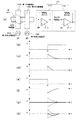
これより本実施形態に係る位置検出装置の動作原理を説明する。なお、説明を簡単にするために、X軸電極群107を構成する任意の電極である第1のX軸電極402及び第2のX軸電極403に矩形波を供給した時に、Y軸電極群108の任意の一の電極であるY軸電極406から出力される信号を例示する。
図4(a)、(b)、(c)、(d)、(e)、(f)、(g)及び(h)は、本実施形態に係る位置検出装置101の、等価回路及び波形図である。
この第1のX軸電極402及び第2のX軸電極403とY軸電極406とに着目すると、図3に示す矩形波生成部102、X軸電極群107、Y軸電極群108及びプリアンプ109は、図4(a)に示す等価回路で表すことができる。第1のX軸電極402と第2のX軸電極403に矩形波を供給する矩形波生成部102は、第1のX軸電極402と第2のX軸電極403のそれぞれに矩形波を供給するのだから、それぞれの電極に第1の矩形波電圧源404及び第2の矩形波電圧源405を接続したとみなすことができる。
なお、この図4(a)中では、指407の存在を点線で示している。
[Operating principle]
The operation principle of the position detection apparatus according to this embodiment will be described below. For simplicity of explanation, when a rectangular wave is supplied to the first X-axis electrode 402 and the second X-axis electrode 403 which are arbitrary electrodes constituting the
4 (a), (b), (c), (d), (e), (f), (g) and (h) are equivalent circuits and waveforms of the
Focusing on the first X-axis electrode 402, the second X-axis electrode 403, and the Y-
In FIG. 4A, the presence of the
Y軸電極406は、プリアンプ109に接続されている。このプリアンプ109は、オペアンプ412と抵抗R413とからなる電流電圧変換回路414と、ドライバ418とから構成される。電流電圧変換回路414を構成するオペアンプ412の入力端子は、周知のイマジナルショート現象によって、仮想的にショートした状態が維持される。したがって、Y軸電極406から見ると、接地されたのと等しい状態になる。
The Y-
電流電圧変換回路414は、微弱な電流を電圧に変換すると共に、増幅もする。更に、増幅された電圧信号は、抵抗R415とR416とオペアンプ417とからなる反転増幅器(ドライバ)418に入力され、後続の回路にとってより扱い易い信号レベルまで増幅される。なお、電流電圧変換回路414も反転増幅器の一種であるから、入力される信号は「反転の反転」が行われ、結果として位相が元に戻る。
The current-
次に、指407が電極の交点に近接した場合と近接していない場合とにおける、Y軸電極406に現れる電流波形の違いについて説明する。
図4(b)は、時点t0において、第1矩形波電圧源404から第1のX軸電極402に立ち上がりの電圧を印加した時の、X軸電極402の電圧波形図である。なお、この波形は、第2矩形波電圧源405から第2のX軸電極403へ立上がり電圧を印加した時の波形と同一である。
図4(c)は、時点t0において、第1矩形波電圧源404から第1のX軸電極402に立ち上がりの電圧を印加した時の、Y軸電極406の電流波形図である。
Next, the difference in the current waveform appearing on the Y-
FIG. 4B is a voltage waveform diagram of the X-axis electrode 402 when a rising voltage is applied from the first rectangular
FIG. 4C is a current waveform diagram of the Y-
図4(d)は、時点t0において、第1矩形波電圧源404から第1のX軸電極402に立ち上がりの電圧を印加した時の、Y軸電極406の電流波形図である。
ところで、コンデンサに矩形波の電圧を印加すると、その立ち上がりと立ち下がりの時にのみ、コンデンサに電流が流れる。したがって、第1のX軸電極402とY軸電極406の交点にはコンデンサが形成されているので、このコンデンサにも同様の現象が生じる。
次に、時点t0に立ち上がる矩形波信号をX軸電極に印加した場合について説明する。
指407が電極の交点に近接していない場合、すなわち、第2のX軸電極403に第2矩形波電圧源405から図4(b)に示す矩形波を印加した場合は、第2のX軸電極403とY軸電極406との間に構成されるコンデンサには、その印加した矩形波信号の立ち上がり時にのみ電流が流れる。したがって、このコンデンサに流れる電流は図4(c)に示す波形となる。
FIG. 4D is a current waveform diagram of the Y-
By the way, when a rectangular wave voltage is applied to the capacitor, a current flows through the capacitor only at the rise and fall. Therefore, since a capacitor is formed at the intersection of the first X-axis electrode 402 and the Y-
Next, a case where a rectangular wave signal that rises at time t0 is applied to the X-axis electrode will be described.
When the
これに対し、指407が電極の交点に近接している場合、すなわち、第1の矩形波電圧源404が図4(b)に示す矩形波信号を第1のX軸電極402に印加した場合は、第1のX軸電極402から発される電気力線の一部が指407に吸収される。その結果、電極の交点に指407が近接していない場合(図4(c))に比べて、その交点に指407が近接する場合(図4(d))の電極の交点に形成されるコンデンサの静電容量は減少するので、図4(d)は図4(c)と比べて電流波形の総面積が小さくなっている。周知の通り、電流波形の総面積は、コンデンサに蓄電された電荷に相当する。
In contrast, when the
次に、時点t0に立ち下がる矩形波信号をX軸電極に印加した場合について説明する。
ここで、図4(e)は、時点t0において、第2矩形波電圧源405から第2のX軸電極403に立ち下がりの電圧を印加した時の、第2のX軸電極403の電圧波形図である。なお、この波形は、第1矩形波電圧源404から第1のX軸電極403へ立ち下がり電圧を印加した時の波形と同一である。
図4(f)は、時点t0において、第2矩形波電圧源405から第2のX軸電極403に立ち下がりの電圧を印加した時の、Y軸電極406の電流波形図である。図4(f)の電流波形は、図4(c)の波形とは位相が180°反転した波形となっている。
Next, a case where a rectangular wave signal that falls at time t0 is applied to the X-axis electrode will be described.
Here, FIG. 4E shows the voltage waveform of the second X-axis electrode 403 when a falling voltage is applied from the second rectangular
FIG. 4F is a current waveform diagram of the Y-
次に、第1のX軸電極402と第2のX軸電極403の双方に、時刻t0の時点で同時に矩形波信号を印加した場合について説明する。ここで、図4(g)は、時点t0において、第1のX軸電極402とY軸電極406との交点に指407が近接していない状態で、第1矩形波電圧源404から第1のX軸電極402に立ち上がりの電圧を印加すると同時に、第2矩形波電圧源405から第2のX軸電極403に立ち下がりの電圧を印加した時の、Y軸電極406の電流波形図である。すなわち、この図4(g)に示す電流波形は、図4(c)と図4(f)との合成波形である。
図4(h)は、第1のX軸電極402とY軸電極406の交点に指407が近接している状態で、時点t0において、第1矩形波電圧源404から第1のX軸電極402に立ち上がりの電圧を印加すると同時に、第2矩形波電圧源405から第2のX軸電極403に立ち下がりの電圧を印加した時の、Y軸電極406の電流波形図である。すなわち、この図4(h)に示す電流波形は、図4(d)と図4(f)の合成波形である。
Next, a case where a rectangular wave signal is simultaneously applied to both the first X-axis electrode 402 and the second X-axis electrode 403 at time t0 will be described. Here, FIG. 4G shows the first rectangular
FIG. 4H shows the first X-axis electrode from the first rectangular
図4(a)に示す指407が第1のX軸電極403とY軸電極406との交点に近接していない場合について説明する。
時点t0において、第1矩形波電圧源404が第1のX軸電極402に立ち上がり電圧(図4(b))を印加し、第2矩形波電圧源405が第2のX軸電極403に立ち下がり電圧(図4(e))を印加したとすると、第1のX軸電極402とY軸電極406の交点によって形成されるコンデンサの静電容量と、第2のX軸電極403とY軸電極406の交点によって形成されるコンデンサの静電容量が等しくなるので、それぞれの交点に発生する電流が打ち消し合う。その結果、Y軸電極406には、電流波形は発生しない。
A case where the
At time t0, the first rectangular
これに対し、図4(a)に示すように、時点t0において、指407が第1のX軸電極403とY軸電極406との交点に近接している場合に、第1矩形波電圧源404が第1のX軸電極402に立ち上がり電圧(図4(b))を印加し、第2矩形波電圧源405が第2のX軸電極403に立ち下がり電圧(図4(e))を印加したとすると、第1のX軸電極402とY軸電極406の交点によって形成されるコンデンサの静電容量は、第2のX軸電極403とY軸電極406の交点によって形成されるコンデンサよりも静電容量が減少している。その結果、Y軸電極406には負方向に電流波形が発生する。
On the other hand, as shown in FIG. 4A, when the
以上に説明したように、X軸電極とY軸電極との交点に指407が近接すると、その交点によって形成されるコンデンサの静電容量が減少する。静電容量が減少した交点に立ち上がりあるいは立ち下がりの電圧変化を加え、他の交点に現れる電圧変化によって生じる電流との合成電流波形が、Y軸電極に現れる。
As described above, when the
次に、先に図4で説明した指の存在を検出する仕組みを踏まえて、本実施形態で高速に指の存在を検出する動作原理を説明する。
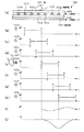
図5は、マトリクス電極103の一部断面図と、X軸電極に電圧を印加する状態と、発生する電流波形及び電流積分波形とを示す図である。
Next, based on the mechanism for detecting the presence of the finger described above with reference to FIG. 4, the operation principle for detecting the presence of the finger at high speed in this embodiment will be described.
FIG. 5 is a partial cross-sectional view of the
図5(a)は、マトリクス電極103の、図1のA−A‘における一部断面図である。
前述したように、マトリクス電極103は、X軸電極群107と、Y軸電極群108とを有しており、このX軸電極群107とY軸電極群108との間に介在して設けられた第一の絶縁シート506とを備える。さらに、マトリクス電極103は、X軸電極群108が第一の絶縁シート505と対向する面と反対の面側に第二の絶縁シート506を備える。
第一の絶縁シート505は、例えば、略板状の絶縁材で、X軸電極群107とY軸電極群108との各交点を絶縁させるためのものである。
第二の絶縁シート506は、略板状の絶縁材で、位置を指示する際に指407が、X軸電極107a〜107gに直接触れないように、この第二の絶縁シート506によって覆われている。したがって、この第二の絶縁シート506の直下に、X軸電極107a〜107gが位置するので、X軸電極群107から発される電気力線は、効果的に指407に吸収される。
FIG. 5A is a partial cross-sectional view of the
As described above, the
The first insulating
The second
図5(b)、(c)、(d)、(e)、(f)、(g)及び(h)は、X軸電極群107のうちの任意のX軸電極107a〜107gに印加される電圧のタイミングを示す波形図である。ここで、図5(b)〜(h)中の時点t1〜t7は、各X軸電極107a〜107gにワンショットパルスが印加された時点を示しており、時点t2は時点t1から1クロック後を示し、同様に、各時点tnはt(n−1)から1クロック後の時点を示している。
5B, 5C, 5D, 5E, 5G, and 5H are applied to arbitrary
ところで、前述したように、矩形波生成部102は、シフトレジスタ209の有効ビットセル209aに値「1」が入力されたときに、この有効ビットセル209aに接続されているX軸電極107aに電圧を印加する。そして、矩形波生成部102は、この有効ビットセル209aに値「1」が入力されている間、X軸電極107aに電圧を印加し続ける。その後、矩形波生成部102は、有効ビットセル209aに値「0」が入力されたときに、X軸電極107aへの電圧の印加を終了する。ここで、シフトレジスタ209がX軸電極107aに印加する電圧の幅は、分周器203において分周され出力されたクロックを使用しており、値「1」は連続して3回、シフトレジスタ209に入力されるから、シフトレジスタ209に入力されたクロックの3回分に相当するワンショットパルスとなる。その結果、例えば、X軸電極107aにワンショットパルスが印加された時点t1を基準とすると、X軸電極107aに印加されたワンショットパルスの立ち下がりは、時点t4に訪れることになる。
By the way, as described above, when the value “1” is input to the
以上のように、矩形波生成部102は、この矩形波生成部102のシフトレジスタ209に接続されているX軸電極107a〜107gにワンショットパルスを印加するから、各X軸電極107a〜107gのうち、立ち上がり時点と立ち下がり時点とが同時となるワンショットパルスの組、例えば、X軸電極107cに印加されるワンショットパルスの立ち下がり時点でY軸電極108eに発生する電流と、X軸電極107fに印加されるワンショットパルスの立ち上がり時点でY軸電極108eに発生する電流とが合成されて、図4にて説明した原理で相殺されるから、Y軸電極108eには電流波形が発生しない。同様に、同一の時点(例えば、時点t6)に立ち上がるワンショットパルスと、立ち下がるワンショットパルスとが存在する場合には、Y軸電極108eには電流が発生せず、X軸電極群107の各X軸電極の全てにワンショットパルスを印加した場合にも、同様に電流波形は発生しないことになる。
As described above, since the rectangular
ところが、図5(a)に示すように、X軸電極107eとY軸電極108eとの交点には指407が近接しているので、X軸電極107eと107hとのそれぞれに印加したワンショットパルスによりY軸電極108eに発生するそれぞれの電流同士を合成しても0にならない。その結果、Y軸電極108eには、図5(i)に示すように、指407が近接しているX軸電極107eと107hとに印加されたワンショットパルスの立ち上がりが現れるt4時点と、矩形波電圧の立ち下がりが現れるt7時点とに電流波形が現れる。
However, as shown in FIG. 5A, since the
図5(j)は、Y軸電極503に現れる電流波形を積分した波形である。位置算出部106内の積算部302の出力データを仮想的にアナログ表現にしたものである。
図5(i)に示すように、Y軸電極108eに現れる電流波形は、ゼロ電位を中心にほぼ対称な正弦波交流波形である。そこで、この電流波形をそのまま積分をすれば、図5(j)に示されるように、負方向にピークを持つ波形が得られる。ピーク検出部304は、この波形のピークに最も近いサンプルクロックの値を捉える。そして、重心演算部305はピーク検出部304が得た値と、その前後の値の、三つの値を基に重心演算を行う。
FIG. 5J is a waveform obtained by integrating the current waveform appearing at the Y-
As shown in FIG. 5 (i), the current waveform appearing on the Y-axis electrode 108e is a sine wave AC waveform that is substantially symmetrical about the zero potential. Therefore, if this current waveform is integrated as it is, a waveform having a peak in the negative direction is obtained as shown in FIG. The
重心演算部305は、マトリクス電極103のX軸方向とY軸方向のピークを示す位置を特定するために、カウンタ306からX軸方向のアドレスデータを、受信選択スイッチ104からY軸方向のアドレスデータを受け取る。そして、それらアドレスデータと重心演算の結果を基に、真のピーク値とその時間軸上の位置を算出する。算出した結果、重心演算部305は、マトリクス電極103に近接した指の位置を示す位置データを出力する。
The center-of-
X軸電極107a〜107gの各々に与えられるワンショットパルスは、200kHzの半周期分である。一方で、X軸電極107a〜107gの各々に与えられるワンショットパルスの印加タイミングが、200kHzの整数倍である。本実施形態の場合では、3倍である。
ここで、X軸電極群107全体を縦方向に見ると、3倍の速度で走査を行っていることと等しいものと見ることができる。
The one-shot pulse given to each of the
Here, when the entire
従来技術では、200kHzの交流を複数周期分同期検波して、積分する必要があった。仮に、従来技術の同期検波及び積分を一周期分にして設計したとしても、200kHzの制約があるため、根本的な速度の改善が見込めなかった。
本実施形態は、従来技術がなしえなかった「200kHzの壁」を破る技術の一実装形態である。
In the prior art, it has been necessary to detect and integrate 200 kHz alternating current for a plurality of periods. Even if the conventional synchronous detection and integration is designed for one period, the fundamental speed improvement cannot be expected due to the limitation of 200 kHz.
This embodiment is an implementation form of a technology that breaks the “200 kHz wall” that cannot be achieved by the conventional technology.
ここで、X軸電極群107に、位相をシフトさせたワンショットパルスを順次与える際、Y軸電極群108ではワンショットパルスの立ち上がりと立ち下がりを同時に捉えて、その差を検出できるようにする必要がある。位相シフトの周波数が200kHzの整数倍であるのはこのためである。
Here, when sequentially applying one-shot pulses whose phases are shifted to the
本実施形態は、以下のような応用例が考えられる。
(1)X軸電極群107の各電極に印加される信号の波形は、必ずしも矩形波でなくてもよい。
例えば、0Vから所定の電圧に至るまでの期間、つまり立ち上がりの期間と、所定の電圧から0Vに至るまでの期間、つまり立ち下がりの期間との、電圧の積分値がそれぞれ同じであれば、図4(g)に示した、電流変化の打ち消し合いの効果が得られる。
例えば、シフトレジスタ208の各有効ビットセル209a〜209mとX軸電極群107の各電極との間に、200kHzを通過させるバンドパスフィルタを挿入する。すると、X軸電極群107の各電極には、サイン波形の半波長が印加されることとなる。このような波形でも、指の存在を検出する効果は変わらない。
In this embodiment, the following application examples can be considered.
(1) The waveform of a signal applied to each electrode of the
For example, if the integrated values of the voltage in the period from 0 V to the predetermined voltage, that is, the rising period, and the period from the predetermined voltage to 0 V, that is, the falling period are the same, The effect of canceling out the change in current shown in 4 (g) can be obtained.
For example, a band pass filter that passes 200 kHz is inserted between each
(2)また、X軸電極群107に印加する電圧も高電位と低電位とは相対的な関係であることから、必ずしも低電位の電圧は0Vでなくてもよい。
(2) Since the voltage applied to the
(3)更に、X軸電極群107の各々に与える、周期をずらしたワンショットパルスの周期は、必ずしも厳密に200kHzの整数倍の周波数でなくてもよい。周期のずれは波形となって現れるが、マトリクス電極103に指を近づけることによって生じる、X軸電極とY軸電極との交点に存在する静電容量の変化は、指を近づけていない状態よりも大きい信号の変化となって現れるからである。
(3) Furthermore, the period of the one-shot pulse with a shifted period that is given to each of the
本実施形態においては、静電式の位置検出装置を開示した。
X軸電極の各々に、200kHzの整数倍の周波数に相当する周期をずらしてワンショットパルスを与え、ワンショットパルスの立ち上がり及び立ち下がりの時点に生じる電流変化をY軸電極から検出する。こうすることにより、従来技術がなしえなかった「200kHzの壁」を破り、検出面を分割する等の複雑な回路構成を採用することなく、広大な検出面積を備える静電式位置検出装置を実現できる。
In the present embodiment, an electrostatic position detection device has been disclosed.
A one-shot pulse is applied to each of the X-axis electrodes while shifting a period corresponding to a frequency that is an integral multiple of 200 kHz, and current changes that occur at the rise and fall times of the one-shot pulse are detected from the Y-axis electrode. By doing so, an electrostatic position detection device having a vast detection area can be obtained without using a complicated circuit configuration such as breaking the “200 kHz wall” that could not be achieved by the prior art and dividing the detection surface. realizable.
以上、本発明の実施形態例について説明したが、本発明は上記実施形態例に限定されるものではなく、特許請求の範囲に記載した本発明の要旨を逸脱しない限りにおいて、他の変形例、応用例を含むことは言うまでもない。 The embodiment of the present invention has been described above. However, the present invention is not limited to the above-described embodiment, and other modifications may be made without departing from the gist of the present invention described in the claims. It goes without saying that application examples are included.
101…位置検出装置、102…矩形波生成部、103…マトリクス電極、104…受信選択スイッチ、105…A/D変換器、106…位置算出部、107…X軸電極群、108…Y軸電極群、109…プリアンプ、202…クロック生成器、203…分周器、204…ANDゲート、205…デジタルコンパレータ、206…カウンタ、207…定数n、208…シフトレジスタ、209a〜209m…有効ビットセル、210a、210b、210c…無効ビットセル、211…モノステーブルマルチバイブレータ、302…積算部、303…バッファメモリ、304…ピーク検出部、305…重心演算部、306…カウンタ、402…第1のX軸電極、403…第2のX軸電極、404…第1矩形波電圧源、405…第2矩形波電圧源、406…Y軸電極、407…指、412…オペアンプ、R413…抵抗、414…電流電圧変換回路、R415、R416…抵抗、417…オペアンプ、418…ドライバ、419…反転増幅器、107a、107b、107c、107d、107e、107f、107g…X軸電極、108e…Y軸電極、505…絶縁シート、506…誘電シート
DESCRIPTION OF
Claims (5)
前記信号供給電極と絶縁状態で且つ直交に配置される複数の導体よりなる受信電極と、
所定の低電位から所定の高電位に至るまでの立ち上がり期間の積分値と、前記所定の高電位から前記所定の低電位に至るまでの立ち下がり期間の積分値とが同一となる入力信号を生成し、前記入力信号を、前記信号供給電極の各々に一定の遅延時間をおいて順次供給する信号供給部と、
前記受信電極の一を選択する受信選択スイッチと、
前記信号供給部及び前記受信選択スイッチから得られる情報と、前記信号供給電極と前記受信電極との交点の電気的変化とから位置データを算出する位置算出部と
を具備する位置検出装置。 A signal supply electrode comprising a plurality of conductors arranged in parallel to each other;
A receiving electrode comprising a plurality of conductors that are insulated and orthogonal to the signal supply electrode;
Generates an input signal in which the integral value of the rising period from the predetermined low potential to the predetermined high potential is the same as the integrated value of the falling period from the predetermined high potential to the predetermined low potential A signal supply unit that sequentially supplies the input signal to each of the signal supply electrodes with a certain delay time;
A reception selection switch for selecting one of the reception electrodes;
A position detection apparatus comprising: a position calculation unit that calculates position data from information obtained from the signal supply unit and the reception selection switch, and an electrical change at an intersection of the signal supply electrode and the reception electrode.
請求項1に記載の位置検出装置。 The input signal is a one-shot pulse;
The position detection device according to claim 1.
請求項1又は2に記載の位置検出装置。 The delay time is an integer fraction of the time during which the input signal is supplied to the signal transmission electrode.
The position detection device according to claim 1 or 2.
前記受信選択スイッチから得られる信号をデータに変換して前記位置算出部に出力するA/D変換器と
を備え、
前記位置算出部は、
前記A/D変換器から得られる前記データを積算する積算部と、
前記積算部が出力する積算データを記憶するバッファメモリと、
前記バッファメモリに記憶されている前記積算データのピーク値を検出するピーク検出部と、
前記バッファメモリ及び前記ピーク検出部の出力データを基に、複数の前記積算データの重心を演算する重心演算部と
を有する、請求項1又は2又は3に記載の位置検出装置。 Furthermore,
An A / D converter that converts a signal obtained from the reception selection switch into data and outputs the data to the position calculation unit;
The position calculation unit
An integration unit for integrating the data obtained from the A / D converter;
A buffer memory for storing integration data output by the integration unit;
A peak detector for detecting a peak value of the accumulated data stored in the buffer memory;
4. The position detection device according to claim 1, further comprising: a centroid calculating unit that calculates centroids of a plurality of the accumulated data based on output data of the buffer memory and the peak detecting unit.
相互に平行に配置される複数の導体よりなる信号供給電極の各々に、前記入力信号を、一定の遅延時間をおいて順次供給するステップと、
前記信号供給電極と絶縁状態で且つ直交に配置される複数の導体よりなる受信電極の一を選択するステップと、
前記信号供給電極に前記入力信号が供給されている状態の情報と、前記受信電極の一を選択している状態の情報と、人体が近接することによって生じる前記信号供給電極と前記受信電極との交点の電気的変化とから位置データを算出するステップと
を含む、位置検出方法。 Generates an input signal in which the integral value of the rising period from the predetermined low potential to the predetermined high potential is the same as the integrated value of the falling period from the predetermined high potential to the predetermined low potential And steps to
Sequentially supplying the input signal to each of signal supply electrodes composed of a plurality of conductors arranged in parallel with each other with a certain delay time; and
Selecting one of the receiving electrodes comprising a plurality of conductors that are insulated and orthogonal to the signal supply electrode;
Information on a state in which the input signal is supplied to the signal supply electrode, information on a state in which one of the reception electrodes is selected, and the signal supply electrode and the reception electrode generated when a human body approaches Calculating position data from the electrical change of the intersection.
Priority Applications (6)
| Application Number | Priority Date | Filing Date | Title |
|---|---|---|---|
| JP2008203325A JP5229887B2 (en) | 2008-08-06 | 2008-08-06 | Position detection device |
| US12/534,062 US8581857B2 (en) | 2008-08-06 | 2009-07-31 | Position detecting device and position detecting method |
| IL200215A IL200215A (en) | 2008-08-06 | 2009-08-03 | Position detecting device and position detecting method |
| TW98126366A TWI469020B (en) | 2008-08-06 | 2009-08-05 | Position detection device |
| CN200910164142.0A CN101644980B (en) | 2008-08-06 | 2009-08-06 | Position detecting device and position detecting method |
| EP09010187A EP2151743A3 (en) | 2008-08-06 | 2009-08-06 | Position detecting device and position detecting method |
Applications Claiming Priority (1)
| Application Number | Priority Date | Filing Date | Title |
|---|---|---|---|
| JP2008203325A JP5229887B2 (en) | 2008-08-06 | 2008-08-06 | Position detection device |
Publications (3)
| Publication Number | Publication Date |
|---|---|
| JP2010039852A true JP2010039852A (en) | 2010-02-18 |
| JP2010039852A5 JP2010039852A5 (en) | 2011-09-22 |
| JP5229887B2 JP5229887B2 (en) | 2013-07-03 |
Family
ID=41217613
Family Applications (1)
| Application Number | Title | Priority Date | Filing Date |
|---|---|---|---|
| JP2008203325A Active JP5229887B2 (en) | 2008-08-06 | 2008-08-06 | Position detection device |
Country Status (6)
| Country | Link |
|---|---|
| US (1) | US8581857B2 (en) |
| EP (1) | EP2151743A3 (en) |
| JP (1) | JP5229887B2 (en) |
| CN (1) | CN101644980B (en) |
| IL (1) | IL200215A (en) |
| TW (1) | TWI469020B (en) |
Cited By (8)
| Publication number | Priority date | Publication date | Assignee | Title |
|---|---|---|---|---|
| JP2011128857A (en) * | 2009-12-17 | 2011-06-30 | Panasonic Corp | Touch panel device |
| CN102207804A (en) * | 2010-03-31 | 2011-10-05 | 意法半导体亚太私人有限公司 | Capacitive sensing analog front end |
| JP2011238240A (en) * | 2010-04-30 | 2011-11-24 | Atmel Corp | Multi-chip touch screen |
| JP2012098782A (en) * | 2010-10-29 | 2012-05-24 | Minebea Co Ltd | Input device and method for electronic device |
| JP2013080344A (en) * | 2011-10-03 | 2013-05-02 | Rohm Co Ltd | Touch-type input device, controller thereof, control method, and electronic apparatus |
| KR101783485B1 (en) | 2010-08-23 | 2017-09-29 | 가부시키가이샤 재팬 디스프레이 | Touch detecting function display apparatus, driving circuit, driving method of touch detecting function display apparatus and electronic equipmnent |
| CN110108239A (en) * | 2019-05-21 | 2019-08-09 | 东莞维科电池有限公司 | Pole piece new Methods of Quality Information Acquisition method, system and equipment |
| TWI681329B (en) * | 2014-10-02 | 2020-01-01 | 日商半導體能源研究所股份有限公司 | Input device and input/output device |
Families Citing this family (20)
| Publication number | Priority date | Publication date | Assignee | Title |
|---|---|---|---|---|
| US8866500B2 (en) | 2009-03-26 | 2014-10-21 | Cypress Semiconductor Corporation | Multi-functional capacitance sensing circuit with a current conveyor |
| JP5442479B2 (en) | 2010-02-05 | 2014-03-12 | 株式会社ワコム | Indicator, position detection device and position detection method |
| CN102576275B (en) * | 2010-08-23 | 2016-08-31 | 谱瑞科技股份有限公司 | mutual capacitance sensing circuit, method and system |
| US9823785B2 (en) | 2010-09-09 | 2017-11-21 | 3M Innovative Properties Company | Touch sensitive device with stylus support |
| US9389724B2 (en) | 2010-09-09 | 2016-07-12 | 3M Innovative Properties Company | Touch sensitive device with stylus support |
| JP2012063843A (en) * | 2010-09-14 | 2012-03-29 | On Semiconductor Trading Ltd | Touch sensor |
| DE102011083042A1 (en) | 2010-11-29 | 2012-05-31 | Dr. Johannes Heidenhain Gmbh | Monitoring unit and method for monitoring position signals of incremental position-measuring devices |
| TWI590133B (en) * | 2010-12-31 | 2017-07-01 | 樂金顯示科技股份有限公司 | Apparatus and method for driving touch sensor |
| KR20140026377A (en) | 2011-02-07 | 2014-03-05 | 사이프레스 세미컨덕터 코포레이션 | Noise filtering devices, systems and methods for capacitance sensing devices |
| TWI571788B (en) | 2011-03-21 | 2017-02-21 | 宸鴻光電科技股份有限公司 | Touch sensing device and scanning method thereof |
| US9176621B2 (en) * | 2011-11-18 | 2015-11-03 | Synaptics Incorporated | Flexible timing and multiplexing for a display device comprising an integrated capacitive sensing device |
| JP5733432B2 (en) * | 2012-02-15 | 2015-06-10 | 株式会社村田製作所 | Touch input terminal |
| TW201335820A (en) * | 2012-02-17 | 2013-09-01 | Elan Microelectronics Corp | Anti-noise-interference driving method of touch panel and touch panel using the same |
| US9444452B2 (en) * | 2012-02-24 | 2016-09-13 | Parade Technologies, Ltd. | Frequency hopping algorithm for capacitance sensing devices |
| JP2014092958A (en) * | 2012-11-05 | 2014-05-19 | Panasonic Liquid Crystal Display Co Ltd | Touch detection device, display device and touch detection method |
| CN103197794B (en) * | 2013-03-05 | 2016-03-09 | 北京京东方光电科技有限公司 | A kind of touch detecting method and device |
| CN104854541A (en) * | 2013-09-17 | 2015-08-19 | Avc技术株式会社 | Touch panel device and touch panel drive method |
| US10620737B2 (en) * | 2014-12-08 | 2020-04-14 | Tactual Labs Co. | Differential transmission for reduction of cross-talk in projective capacitive touch sensors |
| JP6713772B2 (en) * | 2016-01-06 | 2020-06-24 | 株式会社ワコム | Position indicator and position indicating method |
| US10437365B2 (en) * | 2017-10-11 | 2019-10-08 | Pixart Imaging Inc. | Driver integrated circuit of touch panel and associated driving method |
Citations (6)
| Publication number | Priority date | Publication date | Assignee | Title |
|---|---|---|---|---|
| JPH06168066A (en) * | 1992-11-30 | 1994-06-14 | Sharp Corp | Display incorprated type tablet device |
| JPH07253851A (en) * | 1994-03-14 | 1995-10-03 | Matsushita Electric Ind Co Ltd | Method for detecting coordinate for tablet incorporated with display device |
| JPH1020992A (en) * | 1996-07-05 | 1998-01-23 | Alps Electric Co Ltd | Coordinate input device |
| JP2003196023A (en) * | 2001-12-27 | 2003-07-11 | Sony Corp | Display device |
| JP2004038919A (en) * | 2002-07-05 | 2004-02-05 | Waso Kagi Kofun Yugenkoshi | Method for detecting object by using a plurality of electric conductors |
| JP2009282680A (en) * | 2008-05-21 | 2009-12-03 | Alps Electric Co Ltd | Input device |
Family Cites Families (18)
| Publication number | Priority date | Publication date | Assignee | Title |
|---|---|---|---|---|
| US3818133A (en) * | 1971-04-05 | 1974-06-18 | W Cotter | Coordinate digitizer incremental system |
| US4686332A (en) * | 1986-06-26 | 1987-08-11 | International Business Machines Corporation | Combined finger touch and stylus detection system for use on the viewing surface of a visual display device |
| US5581274A (en) * | 1991-04-05 | 1996-12-03 | Sharp Kabushiki Kaisha | Display-integrated type tablet device |
| US7911456B2 (en) * | 1992-06-08 | 2011-03-22 | Synaptics Incorporated | Object position detector with edge motion feature and gesture recognition |
| US5606346A (en) * | 1992-12-22 | 1997-02-25 | Matsushita Electric Industrial Co., Ltd. | Coordinate input device |
| JP3368628B2 (en) * | 1993-08-31 | 2003-01-20 | 双葉電子工業株式会社 | Display integrated tablet |
| JP3281256B2 (en) | 1996-04-24 | 2002-05-13 | シャープ株式会社 | Coordinate input device |
| JP3422640B2 (en) * | 1996-11-14 | 2003-06-30 | シャープ株式会社 | Display device with coordinate detection function |
| JP3492493B2 (en) * | 1997-06-13 | 2004-02-03 | 日本電気株式会社 | Touch panel and method of detecting pressed position on touch panel |
| JP3237629B2 (en) * | 1998-10-27 | 2001-12-10 | ぺんてる株式会社 | Direct contact type touch panel device |
| US6621487B2 (en) * | 2000-07-25 | 2003-09-16 | Rohm Co., Ltd. | Circuit for generating touch detection signals, locator device and a method of generating touch detection signals |
| JP3862516B2 (en) * | 2001-05-15 | 2006-12-27 | 富士通株式会社 | Touch panel device |
| WO2006043660A1 (en) * | 2004-10-22 | 2006-04-27 | Sharp Kabushiki Kaisha | Display device with touch sensor, and drive method for the device |
| US7812827B2 (en) * | 2007-01-03 | 2010-10-12 | Apple Inc. | Simultaneous sensing arrangement |
| DE102007001742A1 (en) * | 2007-01-11 | 2008-07-17 | Osram Opto Semiconductors Gmbh | Optoelectronic device and method for producing an optoelectronic device |
| JP4945345B2 (en) * | 2007-07-03 | 2012-06-06 | 株式会社 日立ディスプレイズ | Display device with touch panel |
| EP2327007A4 (en) * | 2008-08-01 | 2012-12-26 | 3M Innovative Properties Co | Touch sensitive devices with composite electrodes |
| JP5396167B2 (en) * | 2009-06-18 | 2014-01-22 | 株式会社ワコム | Indicator detection apparatus and indicator detection method |
-
2008
- 2008-08-06 JP JP2008203325A patent/JP5229887B2/en active Active
-
2009
- 2009-07-31 US US12/534,062 patent/US8581857B2/en active Active
- 2009-08-03 IL IL200215A patent/IL200215A/en active IP Right Grant
- 2009-08-05 TW TW98126366A patent/TWI469020B/en not_active IP Right Cessation
- 2009-08-06 EP EP09010187A patent/EP2151743A3/en not_active Withdrawn
- 2009-08-06 CN CN200910164142.0A patent/CN101644980B/en not_active Expired - Fee Related
Patent Citations (6)
| Publication number | Priority date | Publication date | Assignee | Title |
|---|---|---|---|---|
| JPH06168066A (en) * | 1992-11-30 | 1994-06-14 | Sharp Corp | Display incorprated type tablet device |
| JPH07253851A (en) * | 1994-03-14 | 1995-10-03 | Matsushita Electric Ind Co Ltd | Method for detecting coordinate for tablet incorporated with display device |
| JPH1020992A (en) * | 1996-07-05 | 1998-01-23 | Alps Electric Co Ltd | Coordinate input device |
| JP2003196023A (en) * | 2001-12-27 | 2003-07-11 | Sony Corp | Display device |
| JP2004038919A (en) * | 2002-07-05 | 2004-02-05 | Waso Kagi Kofun Yugenkoshi | Method for detecting object by using a plurality of electric conductors |
| JP2009282680A (en) * | 2008-05-21 | 2009-12-03 | Alps Electric Co Ltd | Input device |
Cited By (8)
| Publication number | Priority date | Publication date | Assignee | Title |
|---|---|---|---|---|
| JP2011128857A (en) * | 2009-12-17 | 2011-06-30 | Panasonic Corp | Touch panel device |
| CN102207804A (en) * | 2010-03-31 | 2011-10-05 | 意法半导体亚太私人有限公司 | Capacitive sensing analog front end |
| JP2011238240A (en) * | 2010-04-30 | 2011-11-24 | Atmel Corp | Multi-chip touch screen |
| KR101783485B1 (en) | 2010-08-23 | 2017-09-29 | 가부시키가이샤 재팬 디스프레이 | Touch detecting function display apparatus, driving circuit, driving method of touch detecting function display apparatus and electronic equipmnent |
| JP2012098782A (en) * | 2010-10-29 | 2012-05-24 | Minebea Co Ltd | Input device and method for electronic device |
| JP2013080344A (en) * | 2011-10-03 | 2013-05-02 | Rohm Co Ltd | Touch-type input device, controller thereof, control method, and electronic apparatus |
| TWI681329B (en) * | 2014-10-02 | 2020-01-01 | 日商半導體能源研究所股份有限公司 | Input device and input/output device |
| CN110108239A (en) * | 2019-05-21 | 2019-08-09 | 东莞维科电池有限公司 | Pole piece new Methods of Quality Information Acquisition method, system and equipment |
Also Published As
| Publication number | Publication date |
|---|---|
| IL200215A0 (en) | 2010-04-29 |
| CN101644980B (en) | 2015-05-27 |
| TWI469020B (en) | 2015-01-11 |
| IL200215A (en) | 2013-06-27 |
| US8581857B2 (en) | 2013-11-12 |
| US20100289758A1 (en) | 2010-11-18 |
| CN101644980A (en) | 2010-02-10 |
| JP5229887B2 (en) | 2013-07-03 |
| EP2151743A2 (en) | 2010-02-10 |
| TW201011622A (en) | 2010-03-16 |
| EP2151743A3 (en) | 2012-10-31 |
Similar Documents
| Publication | Publication Date | Title |
|---|---|---|
| JP2010039852A (en) | Position detection device and method | |
| JP5366681B2 (en) | Position detection device | |
| JP5098042B2 (en) | Position detection apparatus and position detection method | |
| JP2009192306A5 (en) | ||
| JP6298764B2 (en) | Electronic equipment, capacitance sensor and touch panel | |
| CN101369205B (en) | Capacitive detection system and method, and time-interval measurement module and method | |
| US8373671B2 (en) | Touch screen device | |
| JP4850946B2 (en) | Touch panel device | |
| TW201234238A (en) | Demodulated method and system of differential sensing capacitive touch panel with low power | |
| CN102687104A (en) | High speed noise tolerant multi-touch touch device and controller therefor | |
| CN102460357A (en) | High speed multi-touch touch device and controller therefor | |
| JP2015515685A (en) | Method and system for multi-touch decoding | |
| JP2013513173A (en) | Method for scanning a projected capacitive touch panel | |
| JP4913859B2 (en) | Touch panel device | |
| JPWO2018159460A1 (en) | INPUT DEVICE AND ITS CONTROL METHOD | |
| JP2013020479A (en) | Touch panel device | |
| US20090229893A1 (en) | Input device | |
| JP2017511520A (en) | Determination of the touch location on the touch and force sensing surface and the force there | |
| TWI536231B (en) | Multi-touch detection method and device thereof | |
| JP2005134240A (en) | Capacitance detector circuit, capacitance detection method, and fingerprint sensor using the same | |
| KR102047851B1 (en) | Multi channel capacitive touch sensor circuit | |
| US10055033B2 (en) | Active capacitive pen, and touch detection and feedback driving methods therefor | |
| JP5273418B2 (en) | Input device and display device including the same | |
| TWI279770B (en) | The touching sense apparatus | |
| KR20140084876A (en) | Method and apparatus for sensing a plurality of touch inputs |
Legal Events
| Date | Code | Title | Description |
|---|---|---|---|
| A521 | Request for written amendment filed |
Free format text: JAPANESE INTERMEDIATE CODE: A523 Effective date: 20110805 |
|
| A621 | Written request for application examination |
Free format text: JAPANESE INTERMEDIATE CODE: A621 Effective date: 20110805 |
|
| A977 | Report on retrieval |
Free format text: JAPANESE INTERMEDIATE CODE: A971007 Effective date: 20120704 |
|
| A131 | Notification of reasons for refusal |
Free format text: JAPANESE INTERMEDIATE CODE: A131 Effective date: 20120710 |
|
| A521 | Request for written amendment filed |
Free format text: JAPANESE INTERMEDIATE CODE: A523 Effective date: 20120820 |
|
| TRDD | Decision of grant or rejection written | ||
| A01 | Written decision to grant a patent or to grant a registration (utility model) |
Free format text: JAPANESE INTERMEDIATE CODE: A01 Effective date: 20130219 |
|
| A61 | First payment of annual fees (during grant procedure) |
Free format text: JAPANESE INTERMEDIATE CODE: A61 Effective date: 20130314 |
|
| FPAY | Renewal fee payment (event date is renewal date of database) |
Free format text: PAYMENT UNTIL: 20160329 Year of fee payment: 3 |
|
| R150 | Certificate of patent or registration of utility model |
Ref document number: 5229887 Country of ref document: JP Free format text: JAPANESE INTERMEDIATE CODE: R150 Free format text: JAPANESE INTERMEDIATE CODE: R150 |
|
| R250 | Receipt of annual fees |
Free format text: JAPANESE INTERMEDIATE CODE: R250 |
|
| R250 | Receipt of annual fees |
Free format text: JAPANESE INTERMEDIATE CODE: R250 |
|
| R250 | Receipt of annual fees |
Free format text: JAPANESE INTERMEDIATE CODE: R250 |
|
| R250 | Receipt of annual fees |
Free format text: JAPANESE INTERMEDIATE CODE: R250 |
|
| R250 | Receipt of annual fees |
Free format text: JAPANESE INTERMEDIATE CODE: R250 |
|
| R250 | Receipt of annual fees |
Free format text: JAPANESE INTERMEDIATE CODE: R250 |
|
| R250 | Receipt of annual fees |
Free format text: JAPANESE INTERMEDIATE CODE: R250 |
|
| R250 | Receipt of annual fees |
Free format text: JAPANESE INTERMEDIATE CODE: R250 |