JP5366681B2 - Position detection device - Google Patents
Position detection device Download PDFInfo
- Publication number
- JP5366681B2 JP5366681B2 JP2009154203A JP2009154203A JP5366681B2 JP 5366681 B2 JP5366681 B2 JP 5366681B2 JP 2009154203 A JP2009154203 A JP 2009154203A JP 2009154203 A JP2009154203 A JP 2009154203A JP 5366681 B2 JP5366681 B2 JP 5366681B2
- Authority
- JP
- Japan
- Prior art keywords
- electrode
- axis electrode
- input terminal
- unit
- signal
- Prior art date
- Legal status (The legal status is an assumption and is not a legal conclusion. Google has not performed a legal analysis and makes no representation as to the accuracy of the status listed.)
- Expired - Fee Related
Links
Images


Classifications
-
- G—PHYSICS
- G06—COMPUTING; CALCULATING OR COUNTING
- G06F—ELECTRIC DIGITAL DATA PROCESSING
- G06F3/00—Input arrangements for transferring data to be processed into a form capable of being handled by the computer; Output arrangements for transferring data from processing unit to output unit, e.g. interface arrangements
- G06F3/01—Input arrangements or combined input and output arrangements for interaction between user and computer
- G06F3/03—Arrangements for converting the position or the displacement of a member into a coded form
- G06F3/041—Digitisers, e.g. for touch screens or touch pads, characterised by the transducing means
- G06F3/044—Digitisers, e.g. for touch screens or touch pads, characterised by the transducing means by capacitive means
- G06F3/0446—Digitisers, e.g. for touch screens or touch pads, characterised by the transducing means by capacitive means using a grid-like structure of electrodes in at least two directions, e.g. using row and column electrodes
-
- G—PHYSICS
- G06—COMPUTING; CALCULATING OR COUNTING
- G06F—ELECTRIC DIGITAL DATA PROCESSING
- G06F3/00—Input arrangements for transferring data to be processed into a form capable of being handled by the computer; Output arrangements for transferring data from processing unit to output unit, e.g. interface arrangements
- G06F3/01—Input arrangements or combined input and output arrangements for interaction between user and computer
- G06F3/03—Arrangements for converting the position or the displacement of a member into a coded form
- G06F3/041—Digitisers, e.g. for touch screens or touch pads, characterised by the transducing means
- G06F3/044—Digitisers, e.g. for touch screens or touch pads, characterised by the transducing means by capacitive means
- G06F3/0443—Digitisers, e.g. for touch screens or touch pads, characterised by the transducing means by capacitive means using a single layer of sensing electrodes
Abstract
Description
本発明は、位置検出装置に適用して好適な技術に関する。
より詳細には、静電式の位置検出装置の、位置検出平面における走査速度を向上させる技術に関する。
The present invention relates to a technique suitable for application to a position detection device.
More specifically, the present invention relates to a technique for improving a scanning speed in a position detection plane of an electrostatic position detection device.
コンピュータに位置情報を与える入力装置には、様々なものがある。その中で、タッチパネルと呼ばれる、位置情報入力装置がある。
このタッチパネルは、指や専用のペン等の指示体で検出平面に触れることで、コンピュータ等の操作を行う入力装置である。
そして、タッチパネルは、PDA(Personal Digital Assistant)や銀行のATM(Automated Teller Machine)、駅の券売機等で広く利用されている。
There are various input devices that provide position information to a computer. Among them, there is a position information input device called a touch panel.
This touch panel is an input device that operates a computer or the like by touching a detection plane with an indicator such as a finger or a dedicated pen.
The touch panel is widely used in PDA (Personal Digital Assistant), bank ATM (Automated Teller Machine), station ticket machines, and the like.
タッチパネルに採用される位置情報検出技術には、様々なものがある。例えば、圧力の変化で位置検出を行う抵抗膜方式や位置検出平面の表面の膜の静電容量の変化で位置検出を行う静電容量方式等がある。 There are various position information detection techniques employed for touch panels. For example, there are a resistance film method that detects a position by a change in pressure, and a capacitance method that detects a position by a change in capacitance of a film on the surface of a position detection plane.
本発明の従来技術として、静電容量方式による位置検出装置を説明する。
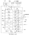
図15は、従来の静電容量方式の位置検出装置を示すブロック図である。
駆動部1502は、例えば人体に最も吸収され易いとされる周波数である、200kHzの交流電圧を生成する。
駆動部1502によって生成された200kHzの交流電圧は、送信選択スイッチ1503を通じて、センサ基板203のX軸方向の電極(以下、「X軸電極」という)209に、選択的に印加される。
このセンサ基板203は、細長い導体の電極を縦横に並べ、縦に並べた電極と、横に並べた電極との間には、図示しない略板状の絶縁シートが介在してコンデンサを形成する。200kHzの交流電圧はこれらコンデンサに印加される。
受信選択スイッチ1504は、コンデンサを形成する交点を定めるためのスイッチである。
受信選択スイッチ1504の出力はプリアンプ1505に供給され、A/D変換器206でデジタルデータに変換された後、位置算出部207aに入力される。
As a prior art of the present invention, a capacitance type position detection device will be described.
FIG. 15 is a block diagram showing a conventional capacitance type position detecting device.
The drive unit 1502 generates an alternating voltage of 200 kHz, which is a frequency that is most easily absorbed by the human body, for example.
The 200 kHz AC voltage generated by the drive unit 1502 is selectively applied to an electrode in the X-axis direction (hereinafter referred to as “X-axis electrode”) 2 09 of the sensor substrate 203 through a transmission selection switch 1503.
The sensor substrate 203 has long and thin conductive electrodes arranged vertically and horizontally, and a capacitor is formed by interposing a substantially plate-shaped insulating sheet (not shown) between the vertically arranged electrodes and the horizontally arranged electrodes. A 200 kHz AC voltage is applied to these capacitors.
The
The output of the
マイコンよりなる位置算出部207aは、同期クロック生成部1506から得られるアドレス情報と、A/D変換器206から得られる僅かな信号変化のデータを受けて、センサ基板203上の指の存在の有無と、その位置の情報とを出力する。具体的には、A/D変換器206から得られたデータを積算処理した後、そのピーク値を検出する。そして、この算出したピーク値とその前後の値を基に重心演算を行う。そして、この得られた重心の時間軸上における位置を基に指の位置を演算する。
なお、説明の便宜のため、センサ基板203のうち、送信選択スイッチ1503に接続されている側の複数の電極をまとめてX軸電極209と呼び、受信選択スイッチ1504に接続されている側の複数の電極をまとめてY軸電極210と呼ぶ。
The
For convenience of explanation, a plurality of electrodes on the side connected to the transmission selection switch 1503 in the sensor board 203 are collectively referred to as an X-axis electrode 209, and a plurality of electrodes on the side connected to the
これより駆動部1502の内部を説明する。
クロック生成器1507はクロックを生成する発振器である。クロック生成器1507が生成したクロックは読み出し部1508に供給される。
サイン波ROM1509は、例えば8ビット×256サンプルの疑似サイン波が記憶されたROMである。読み出し部1508は、クロック生成器1507から供給されるクロックに基づいて、サイン波ROM1509のアドレスを指定して、データを読み出す。
読み出し部1508がサイン波ROM1509から読み出したデータは、D/A変換器1510においてD/A変換された後、LPF1511に入力され、このLPF1511において平滑化されることにより、アナログのサイン波信号に変換される。その後、このアナログサイン波信号は、ドライバ1512において電圧増幅され、X軸電極209に印加される交流電圧となる。
The inside of the drive unit 1502 will now be described.
The
The
The data read from the
なお、本出願人の発明に係る従来技術を、特許文献1及び特許文献2に示す。
The prior arts related to the applicant's invention are shown in
近年、新たなユーザインターフェースの手法として、入力面上の複数の指を同時に検出したい、という要望がある。かかる検出を実現する手法として、例えば、入力面上に存在する複数の指を時分割で順次検出する方法がある。 In recent years, there is a demand for detecting a plurality of fingers on an input surface simultaneously as a new user interface technique. As a method for realizing such detection, for example, there is a method of sequentially detecting a plurality of fingers existing on the input surface in a time division manner.
特許文献1は、受信側のY軸電極を大きく二つ以上の領域に分割し、その分割した領域に属する電極を全て差動増幅器のプラス側入力端子とマイナス側入力端子に接続させ、その領域の境界を移動させる技術内容が開示されている。しかし、この方法では、複数の指の存在をうまく検出することができない。
In
特許文献2には、受信側のY軸電極を構成する全ての電極に、二つのアナログ電子スイッチを接続し、このスイッチに差動増幅器のプラス側入力端子とマイナス側入力端子に接続させている。二つのアナログ電子スイッチを両方共切断すれば、指の存在を検出できない「不感領域」を、位置平面上に設けることが可能になるので、特許文献1と比べると、複数の指の存在を検出することが可能になる。しかし、この方法では、Y軸電極の電極は、差動増幅器のプラス側入力端子に接続されている状態、差動増幅器のマイナス側入力端子に接続されている状態に加えて、差動増幅器のいずれの端子にも接続されていない状態を設けなければならず、制御がより複雑になると共に、部品点数が増加する。
In
本発明はかかる点に鑑みてなされたものであり、最小限の回路構成で、入力面上の複数の指の存在を確実且つ高速に検出する、位置検出装置を提供することを目的とする。 The present invention has been made in view of this point, and an object of the present invention is to provide a position detection device that reliably and rapidly detects the presence of a plurality of fingers on an input surface with a minimum circuit configuration.
上記課題を解決するため、本発明に係る位置検出装置は、略平行に配置された複数の導体からなる第一の電極と、該第一の電極と直交して配置された複数の導体からなる第二の電極と、第一の電極に所定の信号を供給するための信号供給部と、第一及び第二の入力端子を有し、該第一及び第二の入力端子から入力された信号を差動増幅して出力する差動増幅部と、信号供給部に第一の電極のうちから所定の順番で少なくとも一の電極を選択して接続する第一のスイッチ部と、第二の電極を差動増幅部の第一の入力端子又は第二の入力端子のいずれか一方に接続する第二のスイッチ部と、第二のスイッチ部を制御して、第二の電極のうちの隣接する複数の電極を選択してなる第一の選択電極を差動増幅部の第一の入力端子に接続すると共に、第一の選択電極以外の第二の電極のうちから隣接する複数の電極からなる第二の選択電極を差動増幅部の第二の入力端子に接続する制御部と、差動増幅部からの出力信号から指示位置を算出する位置算出部とを具備する。 In order to solve the above problems, a position detection device according to the present invention includes a first electrode composed of a plurality of conductors arranged substantially in parallel and a plurality of conductors arranged orthogonal to the first electrode. A signal having a second electrode, a signal supply unit for supplying a predetermined signal to the first electrode, and first and second input terminals, and signals input from the first and second input terminals A differential amplifying unit that differentially amplifies and outputs the signal, a first switch unit that selects and connects at least one electrode in a predetermined order from the first electrode to the signal supply unit, and a second electrode A second switch unit connected to either the first input terminal or the second input terminal of the differential amplifier unit, and the second switch unit is controlled to be adjacent to the second electrode. The first selection electrode formed by selecting a plurality of electrodes is connected to the first input terminal of the differential amplifier, and A control unit for connecting a second selection electrode composed of a plurality of adjacent electrodes among the second electrodes other than the selection electrode to the second input terminal of the differential amplification unit, and an output signal from the differential amplification unit A position calculation unit for calculating the indicated position from
第二の電極を差動増幅部の第一及び第二の入力端子のいずれかに必ず接続する第二のスイッチ部を設ける。この第二のスイッチ部に対し、第一の入力端子に接続される電極が複数並ぶ第一の選択電極と、第二の入力端子に接続される電極が複数並ぶ第二の選択電極と、第一の選択電極及び第二の選択電極以外の電極とを形成するべく制御する。 A second switch unit is provided that always connects the second electrode to one of the first and second input terminals of the differential amplifier. For the second switch part, a first selection electrode in which a plurality of electrodes connected to the first input terminal are arranged, a second selection electrode in which a plurality of electrodes connected to the second input terminal are arranged, Control is performed to form electrodes other than the first selection electrode and the second selection electrode.
本発明により、最小限の回路構成で、入力面上の複数の指の存在を確実且つ高速に検出可能な、位置検出装置を提供できる。 According to the present invention, it is possible to provide a position detection device capable of reliably and rapidly detecting the presence of a plurality of fingers on an input surface with a minimum circuit configuration.
以下、本発明の実施の形態を、図1〜図14を参照して説明する。 Hereinafter, embodiments of the present invention will be described with reference to FIGS.
図1は本発明の実施の形態の例である位置検出装置の外観斜視図である。本発明の位置検出装置101は、平板状の形状を有する。この位置検出装置101の上面には、長方形の位置検出平面102が設けられている。位置検出平面102の直下には、図2にて後述するセンサ基板が設けられている。この位置検出装置101は、例えば、パーソナルコンピュータやPDA(Personal Digital Assistant)等の図示しない外部装置にケーブル103を介して接続することによって、これら外部装置の入力装置として用いられる。
そして、位置検出装置101は、位置検出平面102上に指104が触れると、位置検出平面102上の指104の位置の情報をケーブル103を通じて、外部装置に出力する。
FIG. 1 is an external perspective view of a position detection apparatus which is an example of an embodiment of the present invention. The position detection device 101 of the present invention has a flat plate shape. A rectangular position detection plane 102 is provided on the upper surface of the position detection apparatus 101. A sensor board, which will be described later with reference to FIG. 2, is provided immediately below the position detection plane 102. The position detection device 101 is used as an input device for these external devices by connecting to an external device (not shown) such as a personal computer or PDA (Personal Digital Assistant) via a cable 103, for example.
Then, when the
図2(a)は、本発明の実施形態の例である、位置検出装置の全体ブロック図である。
位置検出装置101は、矩形波生成部202と、矩形波生成部202に接続されるセンサ基板203と、センサ基板203に接続される信号検出回路201から構成される。信号検出回路201は、センサ基板203に接続される受信選択スイッチ部204と、受信選択スイッチ部204に接続される差動増幅部205と、差動増幅部205に接続されるA/D変換器206と、A/D変換器206に接続される制御部207とから構成される。
FIG. 2A is an overall block diagram of a position detection apparatus, which is an example of an embodiment of the present invention.
The position detection device 101 includes a rectangular
矩形波生成部202は、後述するセンサ基板203を構成するX軸電極209に供給する矩形波形状のワンショットパルスの電圧と、クロックパルスと、リセットパルスとを生成する信号供給部である。この矩形波生成部202によって生成されたクロックパルスは、後述する制御部207内の位置算出部207aに、リセットパルスは、後述するA/D変換器206、位置算出部207a及び制御部207内のスイッチデータ生成部207bに、それぞれ供給される。なお、この矩形波生成部202が生成するワンショットパルスのパルス幅は、例えば、人体に最も吸収され易いとされる200kHzの矩形波から半周期分の信号を取り出したものに等しい、2.5μsecに設定されている。
The rectangular
図2(b)は、センサ基板203の一部断面図である。
センサ基板203は、指示体である人体の指104が位置検出装置101の位置検出平面102上のどの位置に近接したかを検出するためのセンサである。このセンサ基板203は、m本の細長い電極を平行に並べて構成したX軸電極209と、n本の細長い電極を平行に並べて構成したY軸電極210と、X軸電極209とY軸電極210とを絶縁する絶縁シート211と、X軸電極209を保護する絶縁シート212とから構成される。
FIG. 2B is a partial cross-sectional view of the sensor substrate 203.
The sensor substrate 203 is a sensor for detecting which position on the position detection plane 102 of the position detection device 101 the
センサ基板203を構成するX軸電極209とY軸電極210は、絶縁シート211を介して互いに絶縁状態を維持しつつ縦横に並べて構成されている。このため、X軸電極209とY軸電極210との各交点にはコンデンサが形成される。そして、X軸電極209は矩形波生成部202に接続されており、この矩形波生成部202からワンショットパルスが印加される。
The X-axis electrode 209 and the Y-axis electrode 210 constituting the sensor substrate 203 are configured to be arranged vertically and horizontally while maintaining an insulating state with an insulating sheet 211 interposed therebetween. For this reason, a capacitor is formed at each intersection of the X-axis electrode 209 and the Y-axis electrode 210. The X-axis electrode 209 is connected to the rectangular
センサ基板203を構成するX軸電極209とY軸電極210の各々の電極は、指の存在を検出するために適切な間隔を空けて並べられている。本実施形態では、例えば一般的な成人の小指が位置検出平面に接触した際の直径を7〜8mmと想定し、その半分以下の間隔として3.2mmの間隔を以って並べられている。 Each of the X-axis electrode 209 and the Y-axis electrode 210 constituting the sensor substrate 203 is arranged at an appropriate interval in order to detect the presence of a finger. In the present embodiment, for example, a diameter when a general adult little finger contacts the position detection plane is assumed to be 7 to 8 mm, and is arranged with an interval of 3.2 mm as an interval equal to or less than a half thereof.
受信選択スイッチ部204は、Y軸電極210を構成する各電極を、後続の差動増幅部205のプラス側入力端子及びマイナス側入力端子のいずれかに選択的に接続するスイッチである。この受信選択スイッチ部204は、矩形波生成部202と、差動増幅部205とに接続されている。そして、この受信選択スイッチ部204には、矩形波生成部202から出力されたリセットパルスと、スイッチデータ生成部207bから出力された読み出しクロックと、スイッチデータとが供給される。そして、この受信選択スイッチ部204は、センサ基板203から出力された電流を差動増幅部205に出力する。
The reception
差動増幅部205は、受信選択スイッチ部204を介してセンサ基板203から出力される微弱な電流を電圧に変換し、これを増幅してA/D変換器206に出力する。
The
A/D変換器206は、差動増幅部205から入力されたアナログ信号をデジタルデータに変換して位置算出部207aに出力する。
The A /
制御部207は、矩形波生成部202から入力されたアドレス情報を元に、受信選択スイッチ部204を制御して、入力面上の触れた位置を算出して位置情報を出力するマイコンである。この制御部207は、位置算出部207aとスイッチデータ生成部207bとから構成される。
位置算出部207aは、マイコンの一機能部分で、アドレス情報とデジタルデータに所定の演算処理を行い、位置情報を算出する。この位置算出部207aには、A/D変換器206から出力されたデジタルデータ、矩形波生成部202から出力されたクロックパルス及びリセットパルス、及びスイッチデータ生成部207bから出力されたアドレス情報が入力される。そして、位置算出部207aは、これらの入力信号及びデータを基に演算処理を行い、指の存在の有無とその位置情報とを出力する。
The
The
スイッチデータ生成部207bは、受信選択スイッチ部204に設定情報であるスイッチデータを供給する。このスイッチデータ生成部207bには、矩形波生成部202から出力されるリセットパルスと、位置算出部207aから出力される検出Y軸アドレス及び切替信号とが入力される。そして、スイッチデータ生成部207bはこれら入力信号を基にデータ処理を行い、受信選択スイッチ部204にスイッチデータと読み出しクロックとを、位置算出部207aに第一Y軸アドレス及び第二Y軸アドレスを出力する。
ここで、第一Y軸アドレスとは、位置検出平面102全体を早く(粗く)検索するためのアドレスであり、第二Y軸アドレスとは、位置検出平面102の特定箇所を緻密に(微細に)検索するためのアドレスである。
The switch
Here, the first Y-axis address is an address for quickly (coarsely) searching the entire position detection plane 102, and the second Y-axis address is a specific part of the position detection plane 102 that is fine (finely). ) Address for searching.
[矩形波生成部]
次に、矩形波生成部202の構成及び動作について、図3に従って詳述する。
矩形波生成部202は、クロック生成器302と、分周器303と、ANDゲート304と、カウンタ306と、デジタルコンパレータ305と、定数n307と、シフトレジスタ308と、モノステーブルマルチバイブレータ311とから構成される。
[Square wave generator]
Next, the configuration and operation of the rectangular
The rectangular
クロック生成器302は、一定の周波数の矩形波のクロックを生成する発振器である。本実施形態では、クロック生成器302は、例えば12MHz(一周期8.33ns)の矩形波を生成する。クロック生成器302が生成した12MHzのクロックは分周器303に供給される。
分周器303は周知のプログラマブル・カウンタである。そして、この分周器303は、クロック生成器302から入力されるクロックを一定の数だけ計数することで、クロックの周波数を1/Nに変換する。本実施形態では、分周器303の分周比は1/10に設定されており、このクロックは1200kHz(一周期0.833μs)に分周される。
The
The
この分周器303から出力された1200kHzの矩形波信号(以下、単に矩形波と略す)は、クロックパルスとして、ANDゲート304に供給されると共に、シフトレジスタ308及び後述する位置算出部207aにも供給される。
A 1200 kHz rectangular wave signal (hereinafter simply referred to as a rectangular wave) output from the
ANDゲート304は入力デジタル値の論理積を出力する、周知のゲートである。そして、このANDゲート304は、デジタルコンパレータ305から供給される信号が論理値の「真」を示す高電位、すなわち「1」の値が入力されたときにのみ、分周器303から入力されるクロックパルスをカウンタ306に供給する。
The AND
カウンタ306は、入力信号のアップエッジで出力数値をインクリメントさせる周知のカウンタである。カウンタ306の出力数値は、リセット端子に論理値の「真」を示す高電位を与えられるとリセットされる。なお、このカウンタ306は、初期値が「0」に設定されている。このカウンタ306の入力端子はANDゲート304の出力端子に、リセット端子は後述するモノステーブルマルチバイブレータ311にそれぞれ接続されている。
The
そしてカウンタ306は、ANDゲート304からクロックパルスが入力されると、クロックパルスのアップエッジが入力される度に1を加算した計数値(0,1,2,・・・)を出力する。また、カウンタ306は、後述するモノステーブルマルチバイブレータ311から出力されたパルス信号がリセット端子に入力されると、計数値がリセットされ、「0」を出力する。
When the clock pulse is input from the AND
デジタルコンパレータ305は、二つの入力数値の大小を比較する比較器である。このデジタルコンパレータ305は、正入力から入力される数値と負入力から入力される数値とを比較し、正入力から入力された数値の方が大きいときに論理の「真」(=1)を示す高電位を出力する。 The digital comparator 305 is a comparator that compares two input numerical values. The digital comparator 305 compares a numerical value input from a positive input with a numerical value input from a negative input, and indicates logic “true” (= 1) when the numerical value input from the positive input is larger. Output high potential.
そして、デジタルコンパレータ305の正入力には定数n307が、負入力にはカウンタ306がそれぞれ接続されている。したがって、デジタルコンパレータ305は、負入力から入力されるカウンタ306の計数値と、正入力から入力される定数n307の数値とを比較して、定数n307の数値がカウンタ306の出力値より大きいときには、値「1」を出力し、計数値が定数n307の数値と同一又は小さいときには、「0」を出力する。デジタルコンパレータ305による比較結果を示す論理値出力は、ANDゲート304及びシフトレジスタ308に入力される。
A constant n307 is connected to the positive input of the digital comparator 305, and a
定数n307は、レジスタ等で設けられる。この定数n307は、200kHzの自然数倍が与えられる。本実施形態の場合、nは「3」である。この定数n307はデジタルコンパレータ305の正入力へ入力される。 The constant n307 is provided by a register or the like. This constant n307 is given a natural number multiple of 200 kHz. In the present embodiment, n is “3”. This constant n307 is input to the positive input of the digital comparator 305.
シフトレジスタ308は、周知の直列入力・並列出力型のシフトレジスタであり、例えば周知のDフリップフロップをカスケード接続したものである。このシフトレジスタ308は、複数個(m個)の有効ビットセル309a〜309mと、その終端に3個の無効ビットセル310a、310b及び310cとを有する。有効ビットセル309a〜309mは、それぞれがX軸電極209を構成する各電極に接続されている。無効ビットセル310a、310b及び310cにはX軸電極209は接続されない。
無効ビットセル310a、310b及び310cのうちの最後の無効ビットセル310cは、モノステーブルマルチバイブレータ311に接続される。
モノステーブルマルチバイブレータ311の論理値出力は、カウンタ306のリセット端子、受信選択スイッチ部204、位置算出部207a及びスイッチデータ生成部207bに供給される。
The
The last
The logical value output of the monostable multivibrator 311 is supplied to the reset terminal of the
シフトレジスタ308は、分周器303から出力されるクロックパルスのアップエッジに従い、デジタルコンパレータ305の出力値を記憶すると共に、各セルの記憶値を隣接する隣のセル(例えば、有効ビットセル309aであれば、有効ビットセル309b)へずらす。
The
シフトレジスタ308の有効ビットセル309a〜309mは、デジタルコンパレータ305あるいは直前の隣接するセルから論理値「1」が入力され、クロックパルスのアップエッジが入力されると、その論理値「1」が入力された有効ビットセルに接続されているX軸電極209の電極に高電位を出力する。
同様に、シフトレジスタ308の有効ビットセル309a〜309mは、デジタルコンパレータ305あるいは直前の隣接するセルから論理値「0」が入力され、クロックパルスのアップエッジが入力されると、接続されているX軸電極209の電極に低電位を出力する。
The
Similarly, the
各有効ビットセル309a〜309mに論理値「0」が入っているところへ論理値「1」が入力されると、X軸電極209の電位は低電位から高電位に遷移する。
逆に、各有効ビットセル309a〜309mに論理値「1」が入っているところへ論理値「0」が入力されると、X軸電極209の電位は高電位から低電位に遷移する。
つまり、各有効ビットセル309a〜309mに入力される論理値を「0」→「1」→「0」と経時的に変化させることにより、シフトレジスタ308はX軸電極209の各電極にワンショットパルスを供給する。
When a logical value “1” is input to each
Conversely, when a logical value “0” is input to each of the
In other words, the
モノステーブルマルチバイブレータ311は、入力信号(無効ビットセル310cからの信号)の立ち上がりエッジをトリガとして一定幅のパルス信号を出力する。本実施形態では、この一定幅のパルス信号の幅は、上述した矩形波信号のクロックの1クロック以内に設定されている。つまり、モノステーブルマルチバイブレータ311は、無効ビットセル310cが出力する信号の立ち上がりからカウンタ306のリセットパルスを生成するために設けられている。
The monostable multivibrator 311 outputs a pulse signal having a constant width with the rising edge of the input signal (signal from the
以下、矩形波生成部202の動作を詳述する。
カウンタ306の初期値は0であるので、その出力端子から数値「0」を出力する。デジタルコンパレータ305は、定数n307から与えられる数値(n=3)と、カウンタ306から入力される数値「0」とを比較する。この時点では、定数n307の数値の方がカウンタ306から入力される値よりも大きいので、デジタルコンパレータ305は論理値「1」を出力する。ANDゲート304には、上述のデジタルコンパレータ305からの論理値「1」が入力されるので、このANDゲート304は、分周器303から出力されるクロックパルスをカウンタ306に供給する。カウンタ306は、ANDゲート304からクロックパルスが入力されるので、値「1」を出力する。
以降、この値「1」がデジタルコンパレータ305へ入力され、ANDゲート304、カウンタ306及びデジタルコンパレータ305は、カウンタ306からデジタルコンパレータ305へ入力された値が「3」になるまで上記の動作を繰り返す。
Hereinafter, the operation of the rectangular
Since the initial value of the
Thereafter, this value “1” is input to the digital comparator 305, and the AND
カウンタ306からデジタルコンパレータ305へ入力される値が3に達すると、負入力から入力される値(「3」)と、正入力から入力される定数n307の数値「3」とが同じになる。したがって、デジタルコンパレータ305は「偽」、すなわち値「0」を出力する。その結果、ANDゲート206はカウンタ306にクロックパルスを供給しなくなる。したがって、カウンタ306における計数はANDゲート304によって阻止される。これ以降、カウンタ306はANDゲート304によってクロックの供給が止められ、その結果として計数が止まる。すなわち、上記動作を行うと、デジタルコンパレータ305からは、クロックパルスのタイミング毎に「111000・・・」の順で論理値が出力される。
When the value input from the
次に、シフトレジスタ308の動作について説明する。
デジタルコンパレータ305から出力される論理値は、シフトレジスタ308の有効ビットセル309aに供給される。シフトレジスタ308は、分周器303から供給されるクロックパルスのアップエッジに応じて、有効ビットセル309aに保持されている値「1」を隣の有効ビットセル309bへシフトさせると共に、新たにデジタルコンパレータ305から出力された値「1」を有効ビットセル309aに保存する。以降、クロックパルスが入力される毎に、シフトレジスタ308は、特定の有効ビットセル309xの値を隣接する隣の有効ビットセル309(x+1)へ順にシフトさせる。そして、最後の有効ビットセル309mに保持されている値は、最初の無効ビットセル310aに供給される。同様に、最初の無効ビットセル310aに保持されている値は隣接する隣の無効ビットセル310bに、無効ビットセル310bに保持されている値は最後の無効ビットセル310cにそれぞれ供給される。
Next, the operation of the
The logical value output from the digital comparator 305 is supplied to the
そして、最後の無効ビットセル310cに保持された値は、シフトレジスタ308にクロックパルスが入力されると、モノステーブルマルチバイブレータ311に供給される。
このように、シフトレジスタ308がデータを移動させ続けると、最初の段階で入力された「111」という値は、無効ビットセル310a〜310cへ到達する。
The value held in the last
As described above, when the
無効ビットセルの最後のセル310cに論理値「1」が渡ると、セル310cの出力端子は低電位から高電位に推移する。モノステーブルマルチバイブレータ311はこの電圧の推移、つまりアップエッジを受けて、リセットパルスを生成する。リセットパルスはカウンタ306のリセット端子に入力されるので、カウンタ306がリセットされる。
When a logical value “1” is passed to the
その後、モノステーブルマルチバイブレータ311に次の値「1」が入力されると、このモノステーブルマルチバイブレータ311はカウンタ306のリセット入力へのパルス信号の供給をしなくなるので、この時点からカウンタ306は計数が再開する。
このようにして、矩形波生成部202は、X軸電極209にワンショットパルスを供給する。
After that, when the next value “1” is input to the monostable multivibrator 311, the monostable multivibrator 311 does not supply a pulse signal to the reset input of the
In this way, the
次に、位置算出部207aの構成及び位置検出動作について図4に従って詳述する。
Next, the configuration and position detection operation of the
位置算出部207aは、積算部402と、バッファメモリ403と、ピーク検出部404と、重心演算部405と、X軸アドレスカウンタ406とから構成される。
The
積算部402は、A/D変換器206から得られるデジタル値を積算する積分器である。この積算部402は、例えば図示しないメモリと加算器とから構成されている。この積算部402は、矩形波生成部202と、A/D変換器206と、バッファメモリ403とに接続されている。そして、この積算部402は、矩形波生成部202から出力されたクロックパルスが入力される毎に、A/D変換器206から入力されたデジタル値とメモリに記憶されている値とを加算して記憶するとともに、この加算値を出力する。
The
バッファメモリ403は、積算部402の出力値を一時的に記憶するためのRAMである。このバッファメモリ403は、矩形波生成部202と、積算部402と、ピーク検出部404と、重心演算部405とに接続されており、積算部402から出力された加算値を検出データとして記憶する。そして、このバッファメモリ403には、矩形波生成部202から出力されたクロックパルスと、後述するX軸アドレスカウンタ406から出力されたX軸アドレス情報とが入力される。そして、このバッファメモリ403は、クロックパルスが入力されたタイミングに応じて検出データをX軸アドレス情報と共に記憶する。
The
ピーク検出部404は、バッファメモリ403に記憶されている検出データを比較して、この検出データのうち最も値の大きい検出データをピーク値として検出するためのものである。このピーク検出部404は、バッファメモリ403と、重心演算部405とに接続されている。そして、このピーク検出部404において検出されたピーク値は、後段の重心演算部405及び領域判定部407に出力される。
The
重心演算部405は、取得したデータから重心の座標を演算するためのもので、バッファメモリ403と、ピーク検出部404と、カウンタ306と、後述する領域判定部407と、スイッチデータ生成部207bとに接続されている。この重心演算部405には、スイッチデータ生成部207bから出力される第二Y軸アドレスと、矩形波生成部202から出力されるクロックパルスと、後述するX軸アドレスカウンタ406から出力されるX軸アドレスとが入力される。
The center-of-
そして、この重心演算部405は、ピーク検出部404から入力されたピーク値を示すバッファメモリ403上のアドレスと、スイッチデータ生成部207bから入力された第二Y軸アドレスとを基にして、少なくともこのピーク値を示したバッファメモリ403上のアドレス及びこのアドレスの前後のアドレスに記憶されたデータをバッファメモリ403から取得して、これら三つのデータの重心を演算する。
The center-of-
この重心演算部405の演算結果である重心の位置は、センサ基板203上の指の位置、すなわち位置データとなる。
The position of the center of gravity, which is the calculation result of the center of
X軸アドレスカウンタ406は、矩形波生成部202から出力されるクロックパルスを計数するためのもので、その計数値は矩形波生成部202から出力されるリセットパルスでリセットされる。このX軸アドレスカウンタ406の出力値(計数結果)は、X軸電極209を構成する電極のうちの一を選択した値となる。
そして、このX軸アドレスカウンタ406の出力値は、X軸アドレスとして、バッファメモリ403及び重心演算部405に供給される。
The
The output value of the
領域判定部407は、取得したデータから、人体の指が位置検出装置101の位置検出平面102上に存在するか否か、存在するならどの箇所(領域)に存在するのかを判定する。この領域判定部407は、ピーク演算部304とスイッチデータ生成部とに接続されている。そして、この領域判定部407には、スイッチデータ生成部207bから出力される第一Y軸アドレスが入力される。
領域判定部407は、指の存在を検出すると、切替信号と、その指のY座標である第一Y軸アドレスを、検出Y軸アドレスとしてスイッチデータ生成部207bへ出力する。
The
When the
本実施形態の位置検出装置101は、センサ基板203上に存在する指の位置を、二つのモードで探索する。
一つは、センサ基板203を大まかな領域で分割して指の存在を検出する粗探索モードであり、もう一つは、センサ基板203の、指の存在が判明した領域の中で精緻に指の位置を検出する微探索モードである。
領域判定部407は、位置検出装置101が粗探索モードの時に動作し、指の存在の有無と、指の存在する領域を判定する。指の存在とその領域が判明した時は、その旨を示す切替信号をスイッチデータ生成部207bに出力する。
重心演算部405は、位置検出装置101が微探索モードの時に動作し、領域判定部407が検出した指の存在する領域の範囲内で、指の存在する位置を重心演算にて算出する。
位置検出装置101の位置検出平面から指が離れると、重心演算部405は領域判定部407に指が位置検出平面上に存在しない旨の信号を出力する。領域判定部407はこれを受けて、切替信号を再度反転させ、粗探索モードを実行する。
The position detection apparatus 101 according to the present embodiment searches for the position of the finger existing on the sensor substrate 203 in two modes.
One is a rough search mode in which the sensor substrate 203 is divided into rough regions to detect the presence of a finger, and the other is a precise finger detection in the region of the sensor substrate 203 where the presence of the finger is found. This is a fine search mode for detecting the position of.
The
The center-of-
When the finger moves away from the position detection plane of the position detection device 101, the center-of-
次に、矩形波生成部の動作原理を図5及び図6に従って説明する。なお、説明を簡単にするために、X軸電極209を構成する任意の電極である第一のX軸電極502及び第二のX軸電極503に矩形波を供給した時に、Y軸電極210の任意の一の電極である第一のY軸電極506aから出力される信号を例示する。
第一のX軸電極502、第二のX軸電極503及び第一のY軸電極506aに着目すると、図4に示す矩形波生成部202、X軸電極209、Y軸電極210及び差動増幅部205は、図5に示す等価回路で表すことができる。すなわち、この第一のX軸電極502と第二のX軸電極503に矩形波を供給する矩形波生成部202は、第一のX軸電極502と第二のX軸電極503のそれぞれに矩形波を供給するので、第一矩形波電圧源504及び第二矩形波電圧源505とみなすことができる。
なお、この図5中では、指507の存在を点線で示している。
Next, the principle of operation of the rectangular wave generator will be described with reference to FIGS. For simplicity of explanation, when a rectangular wave is supplied to the first
Focusing on the first
In FIG. 5, the presence of the
また、図4に示す差動増幅部205は、第一のY軸電極506aに接続されるオペアンプ512aと抵抗R513aとからなる電流電圧変換回路514aと、第二のY軸電極506bに接続されるオペアンプ512bと抵抗R513bとからなる電流電圧変換回路514bと、電流電圧変換回路514aに接続される抵抗R515a、電流電圧変換回路514bに接続される抵抗R515b及び抵抗R516とオペアンプ517とからなる差動増幅器518とから構成される。
そして、電流電圧変換回路514aを構成するオペアンプ512aの入力端子は、周知のイマジナルショート現象によって、仮想的にショートした状態が維持される。したがって、第一のY軸電極506aから見ると、接地されたのと等しい状態になる。なお、電流電圧変換回路514bも電流電圧変換回路514aと同様である。
4 is connected to a current-
The input terminal of the
電流電圧変換回路514a及び514bは、微弱な電流を電圧に変換して、増幅する。そして、この増幅された電圧信号は差動増幅器518に入力され、後段の回路にとってより扱い易い信号レベルまで増幅される。なお、差動増幅器518は第一のY軸電極506a及び第二のY軸電極506bに同相にて混入するノイズを打ち消す効果がある。
The current-
次に、指507が電極の交点に近接した場合と近接していない場合とにおける、第一のY軸電極506aに現れる電流波形の違いについて説明する。
Next, the difference in current waveform that appears on the first Y-
コンデンサに矩形波の電圧を印加すると、その立ち上がりと立ち下がりの時にのみ、コンデンサに電流が流れる。第一のX軸電極502と第一のY軸電極506aの交点にはコンデンサが形成されているので、この交点に形成されたコンデンサにも同様の現象が生じる。
When a rectangular wave voltage is applied to the capacitor, current flows through the capacitor only at the rise and fall. Since a capacitor is formed at the intersection of the first
したがって、時点t0に立ち上がる矩形波信号をX軸電極に印加すると、指507が電極の交点に近接していない場合、すなわち、第二矩形波電圧源505が第二のX軸電極503に図6(a)に示す矩形波を印加した場合は、第二のX軸電極503と第一のY軸電極506aとの間に構成されるコンデンサには、その印加した矩形波信号の立ち上がり時にのみ電流が流れる。その結果、このコンデンサに流れる電流は図6(b)に示す波形となる。
Accordingly, when a rectangular wave signal rising at time t0 is applied to the X-axis electrode, the
これに対し、指507が電極の交点に近接している場合、すなわち、第一矩形波電圧源504が第一のX軸電極502に図6(a)に示す矩形波信号を印加した場合は、第一のX軸電極502から発される電気力線の一部が指507に吸収される。その結果、電極の交点に指507が近接していない場合(図6(b))に比べて、その交点に指507が近接する場合(図6(c))の電極の交点に形成されるコンデンサの静電容量は減少するので、図6(c)は図6(b)と比べて電流波形の総面積が小さくなっている。なお、周知の通り、電流波形の総面積は、コンデンサに蓄電された電荷に相当する。
On the other hand, when the
また、時点t0に立ち下がる矩形波信号をX軸電極に印加すると、指507が電極の交点に近接していない場合、すなわち、第二矩形波電圧源505が第二のX軸電極503に図6(d)に示す矩形波を印加した場合は、第二のX軸電極503と第一のY軸電極506aとの間に構成されるコンデンサには、その印加した矩形波信号の立ち下がり時にのみ電流が流れる。その結果、このコンデンサに流れる電流は図6(e)に示す波形となる。
When a rectangular wave signal that falls at time t0 is applied to the X-axis electrode, the
次に、第一のX軸電極502と第二のX軸電極503の双方に、時刻t0の時点で同時に矩形波信号を印加した場合について説明する。
Next, a case where a rectangular wave signal is simultaneously applied to both the first
指507が第一のX軸電極502と第一のY軸電極506aとの交点に近接していない場合に、時点t0において立ち上がる矩形波信号(図6(a))を第一のX軸電極502に印加した時の電流波形(図6(b))と、時点t0において立ち下がる矩形波信号(図6(d))を第一のX軸電極502に印加した時の電流波形(図6(e))とを比較すると、両者は時間軸tに対し、線対称の関係になる。そこで、隣接するX軸電極(例えば、第一のX軸電極502と第二のX軸電極503)の一方に図6(a)に示す電圧を、他方に図6(d)に示す電圧を同時に印加すると、第二のY軸電極506bには図6(b)に示す電流と、図6(e)に示す電流とが同時に流れることになる。
すなわち、時点t0において、指507が第一のX軸電極502と第一のY軸電極506aとの交点に近接していない場合に、第一矩形波電圧源504が第一のX軸電極502に立ち上がり電圧(図6(a))を印加し、第二矩形波電圧源505が第二のX軸電極503に立ち下がり電圧(図6(d))を印加したとすると、第一のX軸電極502と第一のY軸電極506aの交点によって形成されるコンデンサの静電容量と、第二のX軸電極503と第一のY軸電極506aの交点によって形成されるコンデンサの静電容量が等しくなるので、それぞれの交点に発生する電流が打ち消し合う。その結果、第一のY軸電極506aには、電流波形は発生しない(図6(f))。
When the
That is, when the
これに対し、指507が第一のX軸電極502と第一のY軸電極506aとの交点に近接している場合に、時点t0において立ち上がる矩形波信号(図6(a))を第一のX軸電極502に印加した時の電流波形(図6(c))と、時点t0において立ち下がる矩形波信号(図6(d))を第一のX軸電極502に印加した時の電流波形(図6(e))とを比較すると、両者は時間軸tに対し、線対称の関係にならない。そこで、隣接するX軸電極(例えば、第一のX軸電極502と第二のX軸電極503)の一方に図6(a)に示す電圧を、他方に図6(d)に示す電圧を同時に印加すると、第一のY軸電極506aには図6(c)に示す電流と、図6(e)に示す電流とが同時に流れることになる。
すなわち、時点t0において、指507が第一のX軸電極502と第一のY軸電極506aとの交点に近接している場合に、第一矩形波電圧源504が第一のX軸電極502に立ち上がり電圧(図6(a))を印加し、第二矩形波電圧源405が第二のX軸電極503に立ち下がり電圧(図6(d))を印加したとすると、第一のX軸電極502と第一のY軸電極506aの交点によって形成されるコンデンサの静電容量は、第二のX軸電極503と第一のY軸電極506aの交点によって形成されるコンデンサよりも静電容量が減少している。その結果、第一のY軸電極506aには負方向に電流波形が発生する(図6(g))。
On the other hand, when the
That is, when the
以上に説明したように、X軸電極とY軸電極との交点に指507が近接すると、その交点に形成されたコンデンサの静電容量が減少する。静電容量が減少した交点に立ち上がりあるいは立ち下がりの電圧変化を加え、他の交点に現れる電圧変化によって生じる電流との合成電流波形が、Y軸電極に現れる。
As described above, when the
一方、第二のY軸電極506bには、図5に示すように、指507は近接していない。したがって、第二のY軸電極506bには電流は生じないこととなる。
差動増幅器518には、第一のY軸電極506aの電流波形を電圧変換した信号と、第二のY軸電極506bの電流波形を電圧変換した信号とが逆位相で入力され、差動増幅される。したがって、指507が第一のX軸電極502と第一のY軸電極506aとの交点に近接している時には、差動増幅器518からは、第一のY軸電極506aに生じた電流波形と同じ波形の電圧信号が出力される。
On the other hand, as shown in FIG. 5, the
The
次に、指の検出動作について、図4及び図7に従って説明する。なお、図7では説明の便宜上、図5の電流電圧変換回路514aから得られる信号の波形について注目する。
Next, a finger detection operation will be described with reference to FIGS. In FIG. 7, attention is paid to the waveform of a signal obtained from the current-
図7(a)は、センサ基板203の、図2のA−A‘における一部断面図である。 FIG. 7A is a partial cross-sectional view of the sensor substrate 203 taken along line A-A ′ of FIG.
図7(b)、(c)、(d)、(e)、(f)、(g)及び(h)は、図7(a)に示すX軸電極209のうちの任意のX軸電極702a〜702gに印加する電圧をタイミングを示す波形図である。ここで、図7(b)〜(h)中の時点t1〜t7は、各X軸電極702a〜702gにワンショットパルスが印加された時点を示しており、時点t2は時点t1から1クロック後を示し、同様に、各時点tnはt(n−1)から1クロック後の時点を示している。
7 (b), (c), (d), (e), (f), (g), and (h) are arbitrary X-axis electrodes among the X-axis electrodes 209 shown in FIG. 7 (a). It is a wave form diagram which shows the timing of the voltage applied to 702a-702g. Here, the time points t1 to t7 in FIGS. 7B to 7H indicate the time points when the one-shot pulses are applied to the
ところで、矩形波生成部202は、シフトレジスタ308の有効ビットセル309aに値「1」が入力されたときに、この有効ビットセル309aに接続されているX軸電極702aに電圧を印加する。そして、矩形波生成部202は、この有効ビットセル309aに値「1」が入力されている間、X軸電極702aに電圧を印加し続ける。その後、矩形波生成部202は、有効ビットセル309aに値「0」が入力されたときに、X軸電極702aへの電圧の印加を終了する。ここで、シフトレジスタ308がX軸電極702aに電圧を印加する時間は、分周器303において分周されて出力されたクロックを使用しているから、値「1」は連続して3回、シフトレジスタ308に入力されるので、シフトレジスタ308に入力されたクロックの3回分に相当する時間となる。その結果、例えば、X軸電極702aにワンショットパルスが印加された時点t1を基準とすると、X軸電極702aに印加されたワンショットパルスの立ち下がりは、時点t4に到達することになる。
Incidentally, when the value “1” is input to the
以上のように、矩形波生成部202は、この矩形波生成部202のシフトレジスタ308に接続されているX軸電極702a〜702gにワンショットパルスを順次印加する。そして、各X軸電極702a〜702gのうち、立ち上がり時点と立ち下がり時点とが同時となるワンショットパルスの組み合わせで発生する電流は相殺されるので、Y軸電極703には電流波形が発生しない。例えば、X軸電極702cに印加されるワンショットパルスの立ち下がり時点でY軸電極703に発生する電流と、X軸電極702fに印加されるワンショットパルスの立ち上がり時点でY軸電極703に発生する電流とが合成される場合がこれに該当する。
同様に、同一の時点(例えば、時点t6)に立ち上がるワンショットパルスと、立ち下がるワンショットパルスとが存在する場合には、Y軸電極603には電流が発生せず、X軸電極702の各X軸電極の全てにワンショットパルスを印加した場合にも、同様に電流波形は発生しないことになる。
As described above, the rectangular
Similarly, the same point in time (e.g., time t6) when the one-shot pulse which rises, and the falling one-shot pulse is present, the current is not generated in the Y-axis electrode 603, the X-axis electrodes 70 2 Similarly, when a one-shot pulse is applied to all the X-axis electrodes, no current waveform is generated.
ところが、図7(a)に示すように、X軸電極602dとY軸電極603との交点には指507が近接しているので、X軸電極602dと、702a及び702gとのそれぞれに印加したワンショットパルスによりY軸電極603に発生するそれぞれの電流同士を合成しても0にならない。その結果、Y軸電極603には、図7(i)に示すように、t4時点とt7時点とに、それぞれ電流波形が現れる。このt4時点には、指507が近接しているX軸電極602dに対し、X軸電極602dに印加されたワンショットパルスの立ち上がりと同時にX軸電極702aに印加されたワンショットパルスの立ち下がりが現れる。また、t7時点には、X軸電極602dに印加されたワンショットパルスの立ち下がりと同時にX軸電極702gに印加されたワンショットパルスの立ち上がりが現れる。
However, as shown in FIG. 7A, since the
図7(j)は、Y軸電極603に現れる電流波形を積分した波形である。位置算出部207a内の積算部402の出力データを仮想的にアナログ表現にしたものである。
図7(i)に示すように、Y軸電極603に現れる電流波形は、ゼロ電位を中心にほぼ対称な正弦波交流波形となる。そこで、この電流波形をそのまま積分をすれば、図7(j)に示すように、負方向にピークを持つ波形が得られる。ピーク検出部404は、この波形のピークに最も近いサンプルクロックの値を捉える。そして、重心演算部405はこのピーク検出部404が得た値と、その前後の値の、三つの値を基に重心演算を行う。
FIG. 7J shows a waveform obtained by integrating the current waveform appearing at the Y-axis electrode 603. The output data of the integrating
As shown in FIG. 7I, the current waveform appearing on the Y-axis electrode 603 is a substantially sine wave AC waveform centered on zero potential. Therefore, if this current waveform is integrated as it is, a waveform having a peak in the negative direction is obtained as shown in FIG. The
重心演算部405は、センサ基板203のX軸方向とY軸方向のピークを示す位置を特定するために、X軸アドレスカウンタ406からX軸方向のアドレスデータを、スイッチデータ生成部207bからY軸方向のアドレスデータを受け取る。そして、これらのアドレスデータと重心演算の結果とを基に、真のピーク値とその時間軸上の位置を算出する。重心演算部405は、算出した結果をセンサ基板203に近接した指の位置を示す位置データとして出力する。
The center-of-
次に、受信選択スイッチ部204の構成及び動作について、図8を参照して説明する。この受信選択スイッチ204は、シフトレジスタ802と、レジスタ803と、NOTゲート804と、切替スイッチ805とから構成されている。
シフトレジスタ802は、直列入力・並列出力型のシフトレジスタであり、複数のセル802a〜802nを有している。このシフトレジスタ802には、後述するスイッチデータ生成部207bから出力された読み出しクロックと、スイッチデータとが入力されるようになっている。そして、このシフトレジスタ802は、スイッチデータ生成部207bから入力された読み出しクロックのタイミングに従って、スイッチデータ生成部207bから入力されたスイッチデータを順次、この複数のセル802a〜802nに入力する。この複数のセル802a〜802nは、それぞれの出力端子がレジスタ803の各セル803a〜803nに接続されている。
レジスタ803は、シフトレジスタ802を構成する複数のセルと同数の複数のセル803a〜803nから構成されている。これらのセル803a〜803nは、例えば、周知のラッチR−S型フリップフロップである。そして、このレジスタ803の各セル803a〜803nには、シフトレジスタ802の各セル802a〜802nから出力された値が入力される。
Next, the configuration and operation of the reception
The
The
NOTゲート804は、レジスタ803に供給するストローブ信号を生成するためのもので、矩形波生成部202から入力されたリセットパルスを反転することで、ストローブ信号を生成する。このストローブ信号が入力されることにより、レジスタ803は、シフトレジスタ802にリセットパルスが入力されるタイミング、すなわちストローブ信号が入力されるタイミングで、各セル803a〜803nに保持されている論理値を、この各セル803a〜803nのそれぞれに接続されているシフトレジスタ802の各セル802a〜802nの値に更新する。さらに、レジスタ803の各セル803a〜803nは、切替スイッチ805の各スイッチ805a〜805nにそれぞれ接続されている。
切替スイッチ805は、シフトレジスタ802及びレジスタ803と同数の、例えば、複数のアナログ電子スイッチ805a〜805nから構成されており、レジスタ803が保持する値に基づいて、Y軸電極210の各電極を選択的に差動増幅部205のプラス側入力端子又はマイナス側入力端子のいずれかに接続する。
The
The change-
図9は、スイッチデータ生成部207bの機能ブロック図である。
マイコンのプログラムにより実現されるスイッチデータ生成部207bは、粗探索データ902と微探索データ903の二種類のデータと、粗探索データ902を読み出す第一読み出し制御部904と、微探索データ903を読み出す第二読み出し制御部905と、第一読み出し制御部904及び第二読み出し制御部905にクロックを供給するための読み出しクロック生成部906と、第一読み出し制御部904及び第二読み出し制御部905が出力するスイッチデータを選択的に出力する切替スイッチ907とよりなる。
なお、図9以降の説明では、Y軸電極210の電極が20本あるものと仮定して説明する。
FIG. 9 is a functional block diagram of the switch
The switch
In the description after FIG. 9, the description will be made assuming that there are 20 electrodes of the Y-axis electrode 210.
第一読み出し制御部904は、図示しないROM或はRAMに格納されている粗探索データ902を、領域判定部407が出力する切替信号と、矩形波生成部202が出力するリセットパルスに基づき、読み出しクロック生成部906が生成する読み出しクロックのタイミングに従って読み出す。
粗探索データ902は、Y軸電極210の各電極が差動増幅部205のどちらの入力端子に接続されるのかを制御するためのスイッチデータである。粗探索データ902の各ビットはシフトレジスタ802に入力されるデータである。つまり、粗探索データ902のビット数は、Y軸電極210の電極の本数に等しい。図9では、粗探索データ902は20ビットで構成されている。
The first
The
第二読み出し制御部905は、図示しないROMに格納されている微探索データ903を、領域判定部407が出力する検出Y軸アドレスと、矩形波生成部202が出力するリセットパルスに基づき、読み出しクロック生成部906が生成する読み出しクロックのタイミングに従って読み出す。
微探索データ903も粗探索データ902と同様に、Y軸電極210の各電極が差動増幅部205のどちらの入力端子に接続されるのかを制御するためのスイッチデータである。つまり、微探索データ903のビット数も、Y軸電極210の電極の本数に等しい。図9では、微探索データ903も20ビットで構成されている。
The second
Similar to the
読み出しクロック生成部906は、第一読み出し制御部904に対して、粗探索データ902を読み出すタイミングのクロックを供給する。この読み出しクロックは、第二読み出し制御部905に対して、微探索データ903を読み出すタイミングのクロックにもなる。
更に、この読み出しクロックは、図8の受信選択スイッチ部204内のシフトレジスタ802にスイッチデータを書き込む際のクロックにもなる。
The read
Further, this read clock also serves as a clock for writing switch data to the
前述の通り、粗探索データ902及び微探索データ903は、Y軸電極210の電極の数と等しい数のビット数を備える。本実施形態の場合、Y軸電極210の電極が20本あるので、粗探索データ902及び微探索データ903は、それぞれ20ビットである。
As described above, the
第一読み出し制御部904は、粗探索データ902の読み出し開始位置を一定の規則で変換した値を第一Y軸アドレスとして領域判定部407へ出力する。
第二読み出し制御部905は、微探索データ903のの読み出し開始位置を一定の規則で変換した値を第二Y軸アドレスとして重心演算部405へ出力する。
また、第一読み出し制御部904が出力するスイッチデータと第二読み出し制御部905が出力するスイッチデータは、切替スイッチ907によって選択的に受信選択スイッチ部204へ出力される。
更に、読み出しクロックも受信選択スイッチ部204へ出力される。
The first
The second
The switch data output from the first
Further, a read clock is also output to the reception
図10は、粗探索データ902及び微探索データ903の内容を説明する模式図である。
図10では、粗探索データ902及び微探索データ903を構成するビットをそれぞれ並べて、各ビットに符号を付している。
FIG. 10 is a schematic diagram for explaining the contents of the
In FIG. 10, the bits constituting the
粗探索データ902は、以下のように構成される。
先ず、ビット位置P1からP4までの、4個のビットの値は「0」である。次に、ビット位置P5からP8までの、4個のビットの値は「1」である。そして、ビット位置P9からP20までの、残りの12個のビットの値は、「0」と「1」が交互に連続して繰り返されるパターンである。
微探索データ903は、以下のように構成される。
先ず、ビット位置P1からP3までの、3個のビットの値は「0」である。次に、ビット位置P4からP6までの、3個のビットの値は「1」である。そして、ビット位置P7からP20までの、残りの14個のビットの値は、「0」と「1」が交互に連続して繰り返されるパターンである。
The
First, the values of the four bits from the bit positions P1 to P4 are “0”. Next, the values of the four bits from the bit positions P5 to P8 are “1”. The values of the remaining 12 bits from the bit positions P9 to P20 are a pattern in which “0” and “1” are alternately repeated.
The
First, the values of the three bits from the bit positions P1 to P3 are “0”. Next, the values of the three bits from the bit positions P4 to P6 are “1”. The values of the remaining 14 bits from the bit positions P7 to P20 are a pattern in which “0” and “1” are alternately repeated.
粗探索データ902及び微探索データ903のいずれも、値が「0」のビットが複数連続し、その後に値が「1」のビットが複数連続し、その後は値が「0」と「1」のビットの組み合わせが複数連続する。
粗探索データ902の、値が「0」のビットが複数連続し、その後に値が「1」のビットが複数連続しているパターンは、「00001111」と並んでいる。
微探索データ903の、値が「0」のビットが複数連続し、その後に値が「1」のビットが複数連続しているパターンは、「000111」と並んでいる。
これに対し、粗探索データ902の、値が「0」と「1」のビットの組み合わせが複数連続して繰り返されるパターンは、「010101010101」と並んでいる。
同様に、微探索データ903の、値が「0」と「1」のビットの組み合わせが複数連続して繰り返されるパターンは、「01010101010101」と並んでいる。
In each of the
A pattern in which a plurality of bits having a value of “0” continues in the
In the
On the other hand, a pattern in which a plurality of combinations of bits having values “0” and “1” in the
Similarly, patterns in the
この、値が「0」と「1」のビットの組み合わせが複数連続して繰り返されるパターンは、Y軸電極210の該当する電極を、差動増幅部205のプラス側入力端子とマイナス側入力端子に、交互に接続する。このため、この領域に指を近づけると、指の存在によって減少した静電容量によって得られる電流の変化が、差動増幅部205のプラス側入力端子とマイナス側入力端子との両方に、逆位相で現れる。したがって、電流変化は相殺され、指の存在が検出できなくなる。
つまり、値が「0」と「1」のビットの組み合わせが複数連続して繰り返されるパターンのスイッチデータは、指の存在を検出しない「不感領域」を形成する。
逆に、値が「0」のビットが複数連続し、その後に値が「1」のビットが複数連続しているパターンのスイッチデータは、指の存在を検出する「有効領域」を形成する。
In this pattern in which a plurality of combinations of bits having values “0” and “1” are repeated continuously, the corresponding electrode of the Y-axis electrode 210 is connected to the plus side input terminal and the minus side input terminal of the
That is, switch data having a pattern in which a plurality of combinations of bits having values “0” and “1” are continuously repeated forms a “dead region” in which the presence of a finger is not detected.
Conversely, switch data having a pattern in which a plurality of bits having a value of “0” are consecutive and a plurality of bits having a value of “1” are subsequently formed forms an “effective area” for detecting the presence of a finger.
特許文献1では、指の存在を検出しない不感領域がなかった。不感領域がない場合、位置検出平面に近接する指が一本だけ存在する場合には、この検出方式が有効である。しかし、指の存在が複数あり得る場合は、位置検出平面をスキャンする際、指の存在を検出する箇所と、指の存在を検出しない箇所とで分割しないと、精緻な検出ができなくなってしまう。
In
Y軸電極210に不感領域を設ける方法としては、特許文献2に示すように、電極を差動増幅部205に接続しない、という手法が考えられる。しかし、この場合、図8の切替スイッチ805を、スリーステート型にしなければならなくなる。また、そのためにシフトレジスタ802及びレジスタ803も、非接続状態を作るための、もう一つ分のビットを必要とする。これは回路規模が大きくなってしまう。
As a method of providing the insensitive region in the Y-axis electrode 210, as shown in
図11(a)、(b)、(c)、(d)、(e)、(f)、(g)、(h)、(i)、(j)、(k)、(l)、(m)、(n)、(o)、(p)、(q)、(r)及び(s)は、スイッチデータ生成部207bが生成し出力するスイッチデータを示す図である。
11 (a), (b), (c), (d), (e), (f), (g), (h), (i), (j), (k), (l), (M), (n), (o), (p), (q), (r), and (s) are diagrams illustrating switch data generated and output by the switch
図11(a)、(b)、(c)及び(d)は、スイッチデータ生成部207bが粗探索モードの時に出力されるスイッチデータの遷移を示す。スイッチデータの「−(マイナス)」は、粗探索データ902の値が「0」のビットに相当し、Y軸電極210の当該電極を差動増幅部205のマイナス側入力端子に接続すべく、切替スイッチ805を制御することを意味する。スイッチデータの「+(プラス)」は、粗探索データ902の値が「1」のビットに相当し、Y軸電極210の当該電極を差動増幅部205のプラス側入力端子に接続すべく、切替スイッチ805を制御することを意味する。
11A, 11B, 11C, and 11D show transitions of switch data output when the switch
図11(a)のスイッチデータの「−(マイナス)」を「0」と、「+(プラス)」を「1」と読み替えると、図9の粗探索データ902のスイッチデータ802aと同じである。つまり、図11(a)は、Y軸電極210の各電極が図11(a)の状態で差動増幅部205のプラス側入力端子或はマイナス側入力端子に接続されていることを示すと共に、図9の粗探索データ902を、第一読み出し制御部904が読み出し位置P20から順番にP1まで読み出して、シフトレジスタ802に書き込んだ結果である。
When “− (minus)” of the switch data in FIG. 11A is replaced with “0” and “+ (plus)” is replaced with “1”, it is the same as the switch data 802a of the
図11(b)は、Y軸電極210の各電極が図11(b)の状態で差動増幅部205のプラス側入力端子或はマイナス側入力端子に接続されていることを示すと共に、シフトレジスタ802が図11(a)の状態から、図9の粗探索データ902を、第一読み出し制御部904が読み出し位置P20から順番にP17まで読み出して、シフトレジスタ802に書き込んだ結果である。
同様に、図11(c)は、Y軸電極210の各電極が図11(c)の状態で差動増幅部205のプラス側入力端子或はマイナス側入力端子に接続されていることを示すと共に、シフトレジスタ802が図11(b)の状態から、図9の粗探索データ902を、第一読み出し制御部904が読み出し位置P16から順番にP13まで読み出して、シフトレジスタ802に書き込んだ結果である。
同様に、図11(d)は、Y軸電極210の各電極が図11(d)の状態で差動増幅部205のプラス側入力端子或はマイナス側入力端子に接続されていることを示すと共に、シフトレジスタ802が図11(c)の状態から、図9の粗探索データ902を、第一読み出し制御部904が読み出し位置P12から順番にP9まで読み出して、シフトレジスタ802に書き込んだ結果である。
FIG. 11B shows that each electrode of the Y-axis electrode 210 is connected to the plus side input terminal or the minus side input terminal of the
Similarly, FIG. 11C shows that each electrode of the Y-axis electrode 210 is connected to the plus side input terminal or the minus side input terminal of the
Similarly, FIG. 11D shows that each electrode of the Y-axis electrode 210 is connected to the plus side input terminal or the minus side input terminal of the
図11(d)の状態から図11(a)の状態に移行するには、シフトレジスタ802が図11(d)の状態から、図9の粗探索データ902を、第一読み出し制御部904が読み出し位置P8から順番にP1まで読み出して、シフトレジスタ802に書き込む。
In order to shift from the state of FIG. 11D to the state of FIG. 11A, the
つまり、シフトレジスタ802が初期状態のときには、一度だけ粗探索データ902の全てのビットをシフトレジスタ802に書き込む(図11(a))。その後は、粗探索データ902の下位ビットから順番に、4ビット(図11(b))、4ビット(図11(c))、4ビット(図11(d))、そして8ビット(図11(a))の順に上位ビットまで読み出して、シフトレジスタ802に書き込む。
以上に述べたように、第一読み出し制御部904は、読み出し位置を変えながら、図9の下から上方向に粗探索データ902を読み出す。つまり、第一読み出し制御部904は、粗探索データ902をループ状に図9の下から上方向へ読み出す。
That is, when the
As described above, the first
図11(e)、(f)、(g)、(h)、(i)、(j)、(k)、(l)、(m)、(n)、(o)、(p)、(q)、(r)及び(s)は、スイッチデータ生成部207bが微探索モードの時に出力されるスイッチデータの遷移を示す。
図11(e)は、Y軸電極210の各電極が図11(e)の状態で差動増幅部205のプラス側入力端子或はマイナス側入力端子に接続されていることを示すと共に、図9の微探索データ903を、第二読み出し制御部905が読み出し位置P20から順番にP1まで読み出して、シフトレジスタ802に書き込んだ結果である。
11 (e), (f), (g), (h), (i), (j), (k), (l), (m), (n), (o), (p), (Q), (r), and (s) show transitions of switch data output when the switch
FIG. 11E shows that each electrode of the Y-axis electrode 210 is connected to the plus side input terminal or the minus side input terminal of the
図11(f)は、Y軸電極210の各電極が図11(f)の状態で差動増幅部205のプラス側入力端子或はマイナス側入力端子に接続されていることを示すと共に、シフトレジスタ802が図11(e)の状態から、図9の微探索データ903を、第二読み出し制御部905が読み出し位置P20のビットだけを読み出して、シフトレジスタ802に書き込んだ結果である。
図11(g)は、Y軸電極210の各電極が図11(g)の状態で差動増幅部205のプラス側入力端子或はマイナス側入力端子に接続されていることを示すと共に、シフトレジスタ802が図11(f)の状態から、図9の微探索データ903を、第二読み出し制御部905が読み出し位置P19のビットだけを読み出して、シフトレジスタ802に書き込んだ結果である。
以下同様に、図11(h)から図11(s)まで、図9の微探索データ903を、第二読み出し制御部905が読み出し位置P18、P17、P16…P7まで、1ビットずつ読み出して、シフトレジスタ802に書き込む。
そして、図11(s)の状態から図11(e)の状態に移行するには、図9の微探索データ903を、第二読み出し制御部905が読み出し位置P6からP1までの、6ビット分のデータを読み出して、シフトレジスタ802に書き込む。
FIG. 11F shows that each electrode of the Y-axis electrode 210 is connected to the plus side input terminal or the minus side input terminal of the
FIG. 11G shows that each electrode of the Y-axis electrode 210 is connected to the plus side input terminal or the minus side input terminal of the
Similarly, from FIG. 11 (h) to FIG. 11 (s), the second
Then, in order to shift from the state of FIG. 11 (s) to the state of FIG. 11 (e), the
但し、微探索モードでは、図11(e)から図11(s)の状態に至るまで、Y軸電極210を遷移させることは行わない。微探索モードは、予め粗探索モードで指の存在する領域を確認した後、その領域内に存在する指の位置を精緻に検出するためのモードである。したがって、微探索モードは、粗探索モードで確認した領域の範囲内だけで探索する。
例えば、粗探索モードの図11(a)で指の存在を認識した場合、微探索モードは図11(e)から図11(j)までの状態を繰り返す。図11(j)から再度図11(e)の状態に移行するには、図9の微探索データ903を、第二読み出し制御部905が読み出し位置P15からP1まで読み出して、シフトレジスタ802に書き込む。
同様に、粗探索モードの図11(b)で指の存在を認識した場合、微探索モードは図11(i)から図11(n)までの状態を繰り返す。図11(n)から再度図11(i)の状態に移行するには、図9の微探索データ903を、第二読み出し制御部905が読み出し位置P11からP1まで読み出し、更に読み出し位置P20からP17まで読み出して、シフトレジスタ802に書き込む。
However, in the fine search mode, the Y-axis electrode 210 is not changed from the state shown in FIG. 11E to the state shown in FIG. The fine search mode is a mode for precisely detecting the position of the finger existing in the area after confirming the area where the finger exists in advance in the coarse search mode. Accordingly, in the fine search mode, the search is performed only within the range of the region confirmed in the coarse search mode.
For example, when the presence of a finger is recognized in FIG. 11A in the coarse search mode, the fine search mode repeats the states from FIG. 11E to FIG. In order to shift from the state shown in FIG. 11 (j) to the state shown in FIG. 11 (e) again, the second
Similarly, when the presence of a finger is recognized in FIG. 11B in the coarse search mode, the fine search mode repeats the states from FIG. 11I to FIG. In order to shift from the state shown in FIG. 11 (n) to the state shown in FIG. 11 (i) again, the second
図12(a)、(b)、(c)、(d)、(e)、(f)、(g)、(h)、(i)、(j)、(k)、(l)、(m)、(n)、(o)、(p)、(q)、(r)、(s)、(t)、(u)、(v)、(w)、(x)、(y)及び(z)は、X軸電極209とY軸電極210の状態の変化を示すタイムチャートである。この図12で示すタイムチャートは、図11(a)及び(b)のスイッチデータを用いた時のタイムチャートを示すものである。
図11(a)のスイッチデータは、図12の時刻t0からt1までの間の図12(g)〜(z)が対応する。同様に、図11(b)は、図12の時刻t2からt3までの間の図12(g)〜(z)が対応する。
つまり、図12は、粗探索モードにおけるX軸電極209とY軸電極210の状態の変化を示すタイムチャートであり、Y軸電極210が図11(a)と図11(b)の状態を抜粋して示す図である。
12 (a), (b), (c), (d), (e), (f), (g), (h), (i), (j), (k), (l), (M), (n), (o), (p), (q), (r), (s), (t), (u), (v), (w), (x), (y ) And (z) are time charts showing changes in the states of the X-axis electrode 209 and the Y-axis electrode 210. The time chart shown in FIG. 12 is a time chart when the switch data of FIGS. 11A and 11B is used.
The switch data in FIG. 11A corresponds to FIGS. 12G to 12Z from time t0 to time t1 in FIG. Similarly, FIG. 1 1 (b) is a diagram between the time t2 in FIG. 1 2 to t3 12 (g) ~ (z ) correspond.
That is, FIG. 12 is a time chart showing changes in the states of the X-axis electrode 209 and the Y-axis electrode 210 in the coarse search mode, and the Y-axis electrode 210 extracts the states of FIGS. 11A and 11B. It is a figure shown.
図12(a)〜(f)は、X軸電極209に印加される電圧のタイミングを示す。矩形波生成部202は、図7(b)〜(h)に示す電圧をX軸電極209に印加する。この間、Y軸電極210は一定の状態を維持する。これが、図12のt0からt1までの期間であり、t2からt3までの期間でもある。つまり、図10に示す各パターンは、Y軸電極210の各電極が、矩形波生成部202によるX軸電極209の一周期分のスキャンを実行する時のスイッチデータ(接続パターン)である。
12A to 12F show the timing of the voltage applied to the X-axis electrode 209. FIG. The
したがって、粗探索モードでは、最初に図12(a)の接続パターンを実行し、その次に図12(b)の接続パターンを実行し、その次に図12(c)の接続パターンを実行し、その次に図12(d)の接続パターンを実行する。このために、第一読み出し制御部904はリセットパルスと切替信号に基づき、粗探索データ902の読み出し開始位置を周期的に変更する。
Therefore, in the coarse search mode, the connection pattern shown in FIG. 12A is executed first, the connection pattern shown in FIG. 12B is executed next, and then the connection pattern shown in FIG. 12C is executed. Then, the connection pattern shown in FIG. For this purpose, the first
第一読み出し制御部904によって読み出されたスイッチデータは、切替スイッチ907を介して図8の受信選択スイッチ部204のシフトレジスタ802を通じてレジスタ803に読み込まれる。そして、Y軸電極210の各電極がレジスタ803に読み込まれた接続パターンにて差動増幅部205に接続される。
The switch data read by the first
粗探索モードとは、位置検出平面102上に指が存在するか、存在するとしたらどの領域に存在するのかを大まかに把握するための高速探索モードである。
図13(a)、(b)及び(c)、図14(d)、(e)及び(f)は、粗探索モードの動作を模式的に説明する図である。
The coarse search mode is a high-speed search mode for roughly grasping whether a finger is present on the position detection plane 102 or in which region it is present.
FIGS. 13A, 13B, and 14C, FIGS. 14D, 14E, and 14F are diagrams schematically illustrating the operation in the coarse search mode.
今、使用者が図13(a)に示すように、両手の人差し指で位置検出装置101の位置検出平面1302に触れたとする。
図13(b)は、粗探索モードの最初の段階であり、図13(a)のスイッチデータが図8の受信選択スイッチ部204のシフトレジスタ802を通じてレジスタ803に読み込まれ、Y軸電極210の各電極が図11(a)の接続パターンにて差動増幅部205に接続された状態である。
右手の人差し指で触れた箇所が位置P1303であり、左手の人差し指で触れた箇所が位置P1304である。
Y軸電極210の第一粗領域R1305に属する電極は、差動増幅部205のマイナス側入力端子に接続されているので、負極領域を形成している。
Y軸電極210の第二粗領域R1306の電極は、差動増幅部205のプラス側入力端子に接続されているので、正極領域を形成している。
Y軸電極210の他の領域の電極は、差動増幅部205のプラス側入力端子とマイナス側入力端子に交互に接続されているので、不感領域を形成している。
使用者の左手の人差し指(位置P1304)が位置検出平面1302の第一粗領域R1305に存在するので、この時点で指の存在が検出できる。
Assume that the user touches the
FIG. 13B shows the first stage of the coarse search mode. The switch data in FIG. 13A is read into the
A position touched by the index finger of the right hand is a position P1303, and a position touched by the index finger of the left hand is a position P1304.
Since the electrode belonging to the first rough region R1305 of the Y-axis electrode 210 is connected to the negative side input terminal of the
Since the electrode of the second rough region R1306 of the Y-axis electrode 210 is connected to the plus side input terminal of the
Since the electrodes in other regions of the Y-axis electrode 210 are alternately connected to the positive side input terminal and the negative side input terminal of the
Since the index finger (position P1304) of the user's left hand exists in the first rough region R1305 of the
図13(c)は、粗探索モードの次の段階であり、図13(b)のスイッチデータが図8の受信選択スイッチ部204のシフトレジスタ802を通じてレジスタ803に読み込まれ、Y軸電極210の各電極が図13(b)の接続パターンにて差動増幅部205に接続された状態である。
Y軸電極210の第一粗領域R1305の電極は、差動増幅部205のプラス側入力端子とマイナス側入力端子に交互に接続されているので、不感領域を形成している。
Y軸電極210の第二粗領域R1306の電極は、差動増幅部205のマイナス側入力端子に接続されているので、負極領域を形成している。
Y軸電極210の第三粗領域R1307の電極は、差動増幅部205のプラス側入力端子に接続されているので、正極領域を形成している。
Y軸電極210の他の領域の電極は、差動増幅部205のプラス側入力端子とマイナス側入力端子に交互に接続されているので、不感領域を形成している。
使用者の両手の人差し指(位置P1303及びP1304)が位置検出平面1302上の不感領域に存在するので、この時点では指の存在を検出できない。
FIG. 13C shows the next stage of the coarse search mode. The switch data in FIG. 13B is read into the
Since the electrodes of the first rough region R1305 of the Y-axis electrode 210 are alternately connected to the positive side input terminal and the negative side input terminal of the
Since the electrode of the second rough region R1306 of the Y-axis electrode 210 is connected to the negative side input terminal of the
Since the electrode of the third rough region R1307 of the Y-axis electrode 210 is connected to the plus side input terminal of the
Since the electrodes in other regions of the Y-axis electrode 210 are alternately connected to the positive side input terminal and the negative side input terminal of the
Since the index fingers (positions P1303 and P1304) of both hands of the user are present in the insensitive area on the
図14(d)は、粗探索モードの次の段階であり、図13(c)のスイッチデータが図8の受信選択スイッチ部204のシフトレジスタ802を通じてレジスタ803に読み込まれ、Y軸電極210の各電極が図13(c)の接続パターンにて差動増幅部205に接続された状態である。
Y軸電極210の第一粗領域R1305及び第二粗領域R1306の電極は、差動増幅部205のプラス側入力端子とマイナス側入力端子に交互に接続されているので、不感領域を形成している。
Y軸電極210の第三粗領域R1307の電極は、差動増幅部205のマイナス側入力端子に接続されているので、負極領域を形成している。
Y軸電極210の第四粗領域R1308の電極は、差動増幅部205のプラス側入力端子に接続されているので、正極領域を形成している。
Y軸電極210の第五粗領域R1309の電極は、差動増幅部205のプラス側入力端子とマイナス側入力端子に交互に接続されているので、不感領域を形成している。
使用者の右手の人差し指(位置P1303)が位置検出平面1302上の第四粗領域R1308に存在するので、この時点で指の存在が検出できる。
FIG. 14D shows the next stage of the coarse search mode. The switch data in FIG. 13C is read into the
Since the electrodes of the first rough region R1305 and the second rough region R1306 of the Y-axis electrode 210 are alternately connected to the positive side input terminal and the negative side input terminal of the
Since the electrode of the third rough region R1307 of the Y-axis electrode 210 is connected to the negative side input terminal of the
Since the electrode of the fourth rough region R1308 of the Y-axis electrode 210 is connected to the positive side input terminal of the
Since the electrodes of the fifth rough region R1309 of the Y-axis electrode 210 are alternately connected to the positive side input terminal and the negative side input terminal of the
Since the index finger (position P1303) of the user's right hand exists in the fourth rough region R1308 on the
図14(e)は、粗探索モードの最後の段階であり、図13(d)のスイッチデータが図8の受信選択スイッチ部204のシフトレジスタ802を通じてレジスタ803に読み込まれ、Y軸電極210の各電極が図13(d)の接続パターンにて差動増幅部205に接続された状態である。
Y軸電極210の第一粗領域R1305、第二粗領域R1306及び第三粗領域R1307の電極は、差動増幅部205のプラス側入力端子とマイナス側入力端子に交互に接続されているので、不感領域を形成している。
Y軸電極210の第四粗領域R1308の電極は、差動増幅部205のマイナス側入力端子に接続されているので、負極領域を形成している。
Y軸電極210の第五粗領域R1309の電極は、差動増幅部205のプラス側入力端子に接続されているので、正極領域を形成している。
使用者の右手の人差し指(位置P1303)が位置検出平面1302上の第四粗領域R1308に存在するので、この時点で指の存在が検出できる。
FIG. 14E shows the final stage of the coarse search mode. The switch data in FIG. 13D is read into the
Since the electrodes of the first rough region R1305, the second rough region R1306, and the third rough region R1307 of the Y-axis electrode 210 are alternately connected to the positive side input terminal and the negative side input terminal of the
Since the electrode of the fourth rough region R1308 of the Y-axis electrode 210 is connected to the negative side input terminal of the
Since the electrode of the fifth rough region R1309 of the Y-axis electrode 210 is connected to the plus side input terminal of the
Since the index finger (position P1303) of the user's right hand exists in the fourth rough region R1308 on the
以上の検出結果を基に判断することで、位置検出平面1302の第一粗領域R1305と第四粗領域R1308にそれぞれ指が存在する可能性が認められる。そこで、次に微探索モードに移行する。
微探索モードは、図11(e)〜(s)のうち、指の存在を特定した領域に該当する接続パターンのみを用いる。この時、領域の範囲よりやや広めに探索範囲を設定する。これを示すのが図14(f)である。
By determining based on the above detection results, the possibility that a finger exists in each of the first rough area R1305 and the fourth rough area R1308 of the
In the fine search mode, only the connection pattern corresponding to the region in which the presence of the finger is specified is used in FIGS. 1 1 (e) to (s). At this time, the search range is set slightly wider than the range of the region. This is shown in FIG. 14 (f).
図14(f)で示す第一粗領域R1305を探索するために、図11(e)、(f)、(g)、(h)及び(i)のパターンを用いる。第一粗領域R1305の範囲を探索するだけなら図11(e)、(f)、(g)及び(h)だけでよいが、より確実性を求めるため、図11(i)のパターンも用いる。この時、第一粗領域R1305よりも少し広い、境界線L1310だけ広い範囲で探索を行う。 In order to search for the first rough region R1305 shown in FIG. 14 (f), the patterns of FIGS. 11 (e), (f), (g), (h) and (i) are used. If only the range of the first rough region R1305 is searched, only FIGS. 1 1 (e), (f), (g), and (h) are necessary, but in order to obtain more certainty, the pattern of FIG. 1 1 (i) is used. Also used. At this time, the search is performed in a range that is a little wider than the first rough region R1305 by the boundary line L1310.
図14(f)で示す第四粗領域R1308を探索するために、図11(l)、(m)、(n)、(o)及び(p)を用いる。第四粗領域R1308の範囲を探索するだけなら図11(m)、(n)及び(o)だけでよいが、より確実性を求めるため、図11(l)及び(p)のパターンも用いる。この時、第四粗領域R1308よりも少し広い、境界線L1311及びL1312だけ広い範囲で探索を行う。 In order to search the fourth coarse region R1308 shown in FIG. 14F, FIGS. 1 1 (l), (m), (n), (o) and (p) are used. If only the range of the fourth coarse region R1308 is searched, only FIGS. 1 1 (m), (n), and (o) may be used, but in order to obtain more certainty, the patterns of FIGS. 1 1 (l) and (p) are used. Also used. At this time, the search is performed in a range that is slightly wider than the fourth coarse region R1308 by the boundary lines L1311 and L1312.
図4の領域判定部407は、粗探索モードの時に、上述のように位置検出平面1302上の指の存在と大まかな領域の判定を行う。領域が判定できたら、領域判定部407は切替信号を反転させ、微探索モードに移行すると共に、指の存在を確認した領域の情報を検出Y軸アドレスとして図9の第二読み出し制御部905に出力する。
第二読み出し制御部905は、領域判定部407から与えられた検出Y軸アドレスに基づき、微探索データ903の読み出し位置を変更してスイッチデータとして出力する。
The
The second
前述の通り、粗探索データ902及び微探索データ903の読み出し位置は、Y軸電極210の状態を変更する際に、図11の下から上方向へ変化する。この読み出し位置を一定の規則で変換することで、Y軸電極210の位置、すなわちY軸アドレスに変換することができる。
As described above, the readout positions of the
図13及び図14にて説明したように、不感領域が存在することによって、どの領域に指が存在するのかを確実に特定することが可能になる。 As described with reference to FIGS. 13 and 14, the presence of the insensitive area makes it possible to reliably identify in which area the finger is present.
本実施形態は、以下のような応用例が考えられる。
(1)上述の実施形態では、指の位置を検出するために、粗探索モードと微探索モードの、二つのモードを設けていた。この技術思想を進めて、領域の大きさの違う粗探索モードを複数設け、広大でスキャンが高速な粗探索モードから徐々に領域の大きさを小さくした粗探索モードに移行することが考えられる。丁度、地図の縮尺を拡大するイメージである。
In this embodiment, the following application examples can be considered.
(1) In the above-described embodiment, two modes of the coarse search mode and the fine search mode are provided in order to detect the finger position. By proceeding with this technical idea, it is conceivable that a plurality of coarse search modes having different area sizes are provided, and the coarse search mode in which a large area is scanned at high speed is shifted to a coarse search mode in which the area size is gradually reduced. It is just an image that enlarges the scale of the map.
(2)図10では、不感領域は「0」と「1」のビットが交互に繰り返されるパターンで形成されていたが、指の存在が検出できなくなる、一定の繰り返しパターンを形成するものであれば、この限りでない。例えば、「011001」という繰り返しパターン等がこれに該当する。この場合、Y軸電極210の電極の太さ及び間隔が指の太さに対して十分細かいことが条件となる。
不感領域は、指を検出できる領域(ここでは「有感領域」とする)を構成する、隣接する導体が差動増幅部の同一の端子に接続される本数よりも少ない本数の導体が、差動増幅部の同一の端子に接続されることによって成り立つ。例えば、有感領域が四本の導体の組で成り立つ場合、不感領域は三本以下の導体の組の繰り返しであればよい。
なお、差動増幅部205で信号を打ち消す効果を確実にするため、不感領域を形成する際、「0」のビットの総数と「1」のビットの総数が同一であることが好ましい。
(2) In FIG. 10, the insensitive area is formed with a pattern in which “0” and “1” bits are alternately repeated. However, it may form a certain repetitive pattern in which the presence of a finger cannot be detected. This is not the case. For example, the repeated pattern “011001” corresponds to this. In this case, the condition is that the electrode thickness and interval of the Y-axis electrode 210 are sufficiently fine with respect to the finger thickness.
The insensitive area is an area where a finger can be detected (here, referred to as “sensitive area”). The number of conductors that are less than the number of adjacent conductors connected to the same terminal of the differential amplifier section is the difference. This is achieved by being connected to the same terminal of the dynamic amplification unit. For example, when the sensitive area is composed of a set of four conductors, the insensitive area may be a repetition of a set of three or less conductors.
In order to ensure the effect of canceling the signal by the
本実施形態においては、位置検出装置を開示した。
静電式位置検出装置の受信側の電極を、差動増幅器で検出すると共に、マイナス側入力端子に接続される電極が複数本存在する領域と、プラス側入力端子に接続される電極が複数本存在する領域と、マイナス側入力端子に接続される電極とプラス側入力端子に接続される電極とが交互に存在する領域(不感領域)とを設けた。
この構成を採ることにより、全ての受信側電極は差動増幅器のプラス側入力端子或はマイナス側入力端子のいずれかの端子に必ず接続される構成となる。このため、受信電極と差動増幅器とを接続するスイッチの端子数を少なく、単純な構成にすることができる。また、受信電極が電気的に浮遊した状態がなくなるので、従来技術と比べてノイズの混入が少なくなる。
この結果、従来技術と比べて低コストでありながら複数の指の存在を確実に検出することが可能になる静電式位置検出装置を提供できる。
In the present embodiment, a position detection device has been disclosed.
The reception side electrode of the electrostatic position detection device is detected by a differential amplifier, and there are a plurality of electrodes connected to the negative input terminal and a plurality of electrodes connected to the positive input terminal. An existing region and a region (insensitive region) in which electrodes connected to the minus side input terminal and electrodes connected to the plus side input terminal exist alternately are provided.
By adopting this configuration, all the reception side electrodes are always connected to either the positive side input terminal or the negative side input terminal of the differential amplifier. For this reason, the number of terminals of the switch connecting the receiving electrode and the differential amplifier is small, and a simple configuration can be achieved. In addition, since the receiving electrode is not electrically floated, noise is reduced as compared with the prior art.
As a result, it is possible to provide an electrostatic position detection device that can reliably detect the presence of a plurality of fingers while being low in cost as compared with the prior art.
以上、本発明の実施形態例について説明したが、本発明は上記実施形態例に限定されるものではなく、特許請求の範囲に記載した本発明の要旨を逸脱しない限りにおいて、他の変形例、応用例を含む。 The embodiment of the present invention has been described above. However, the present invention is not limited to the above-described embodiment, and other modifications may be made without departing from the gist of the present invention described in the claims. Includes application examples.
101…位置検出装置、102…位置検出平面、103…ケーブル、104…指、202…矩形波生成部、203…センサ基板、204…受信選択スイッチ部、205…差動増幅部、206…A/D変換器、207a…位置算出部、207b…スイッチデータ生成部、209…X軸電極、210…Y軸電極、302…クロック生成部、303…分周器、304…ANDゲート、305…デジタルコンパレータ、306…カウンタ、307…定数n、308…シフトレジスタ、311…モノステーブルマルチバイブレータ、402…積算部、403…バッファメモリ、404…ピーク算出部、405…重心演算部、406…X軸アドレスカウンタ、407…領域判定部、502…第一のX軸電極、503…第二のX軸電極、504…第一矩形波電圧源、505…第二矩形波電圧源、506a…第一のY軸電極、506b…第二のY軸電極、512a、512b…オペアンプ、514a、514b…電流電圧変換回路、R513a、R513b、R515a、R515b、R516a、R516b…抵抗、517…オペアンプ、518…差動増幅器、507…指、702a、702b、702c、702d、702e、702f、702g…X軸電極、703…Y軸電極、802…シフトレジスタ、803…レジスタ、804…NOTゲート、805…切替スイッチ、902…粗探索データ、903…微探索データ、904…第一読み出し制御部、905…第二読み出し制御部、906…読み出しクロック生成部、907…切替スイッチ DESCRIPTION OF SYMBOLS 101 ... Position detection apparatus, 102 ... Position detection plane, 103 ... Cable, 104 ... Finger, 202 ... Rectangular wave production | generation part, 203 ... Sensor board, 204 ... Reception selection switch part, 205 ... Differential amplification part, 206 ... A / D converter, 207a ... position calculation unit, 207b ... switch data generation unit, 209 ... X axis electrode, 210 ... Y axis electrode, 302 ... clock generation unit, 303 ... frequency divider, 304 ... AND gate, 305 ... digital comparator , 306 ... counter, 307 ... constant n, 308 ... shift register, 311 ... monostable multivibrator, 402 ... accumulator, 403 ... buffer memory, 404 ... peak calculator, 405 ... centroid calculator, 406 ... X-axis address counter , 407 ... area determination unit, 502 ... first X-axis electrode, 503 ... second X-axis electrode, 504 ... first rectangular wave Pressure source, 505 ... second rectangular wave voltage source, 506a ... first Y-axis electrode, 506b ... second Y-axis electrode, 512a, 512b ... operational amplifier, 514a, 514b ... current-voltage conversion circuit, R513a, R513b, R515a , R515b, R516a, R516b ... resistor, 517 ... op amp, 518 ... differential amplifier, 507 ... finger, 702a, 702b, 702c, 702d, 702e, 702f, 702g ... X-axis electrode, 703 ... Y-axis electrode, 802 ... shift Register, 803..., Register, 804... NOT gate, 805... Selector switch, 902... Coarse search data, 903 .. fine search data, 904 .. first read control unit, 905 ... second read control unit, 906. , 907 ... changeover switch
Claims (4)
該第一の方向に対して直交する第二の方向に互いに並列に配置された複数の導体と、
第一の入力端子及び第二の入力端子を備え、該第一の入力端子及び第二の入力端子を介して入力された信号を差動増幅する差動増幅回路を備えた信号検出回路と、
前記第二の方向に互いに並列に配置された複数の導体を前記差動増幅回路の第一の入力端子または第二の入力端子に選択的に供給するための導体選択回路を備えることで、指示体により指示される位置を前記信号検出回路からの出力信号に基づいて検出する位置検出装置であって、
前記第二の方向に互いに並列に配置された複数の導体は、2以上の所定本数からなり互いに隣接する第一の複数導体と第二の複数導体を構成し、
前記選択回路は、前記第一の複数導体を前記差動増幅回路の前記第一の入力端子に接続し、前記第二の複数導体を前記第二の入力端子に接続し、更に、前記第一の複数導体及び前記第二の複数導体以外の導体を互いに隣接する導体が、前記差動増幅回路の異なる入力端子に接続されるように、経時的に選択されるようにした、
位置検出装置。 Predetermined signal is supplied, a plurality of conductors arranged in parallel with each other in a first direction,
A plurality of conductors arranged in parallel with each other in a second direction perpendicular to said first direction,
A signal detecting circuit which includes a differential amplifier circuit to which the first comprises an input terminal and a second input terminal, to differentially amplify the input signal through the input terminals of said first and second input terminals,
By providing a conductor selection circuit for selectively supplying a plurality of conductors arranged in parallel with each other in the second direction to the first input terminal or the second input terminal of said differential amplifier circuit, A position detection device that detects a position indicated by an indicator based on an output signal from the signal detection circuit,
A plurality of conductors arranged in parallel with each other before Symbol second direction constitutes a first plurality conductors and a second plurality conductors that are adjacent to each other consists of two or more predetermined number,
The selection circuit connects the first plurality of conductors to the first input terminal of the differential amplifier circuit, connects the second plurality of conductors to the second input terminal, and further conductors adjacent the multi-conductor and the second conductor other than multiple conductors are to be connected to a different input terminal of said differential amplifier circuit, and to be over time selection,
Position detection device.
該信号供給回路は、前記第一の方向に互いが並列に配置された複数の導体に一定時間間隔で前記信号を順次供給する、
請求項1に記載の位置検出装置。 A signal supply circuit for supplying the predetermined signal;
The signal supply circuit sequentially supplies the signals at a predetermined time interval to a plurality of conductors arranged in parallel with each other in the first direction.
The position detection device according to claim 1.
前記信号供給回路は、前記一定時間間隔は、前記信号のパルス幅の整数倍となるように制御する、
請求項2に記載の位置検出装置。 The signal is a pulse wave having a predetermined width,
The signal supply circuit controls the fixed time interval to be an integral multiple of a pulse width of the signal;
The position detection device according to claim 2 .
請求項3に記載の位置検出装置。 The signal is supplied so that the rising level and the falling level are substantially the same.
The position detection device according to claim 3 .
Priority Applications (4)
| Application Number | Priority Date | Filing Date | Title |
|---|---|---|---|
| JP2009154203A JP5366681B2 (en) | 2009-06-29 | 2009-06-29 | Position detection device |
| TW099119933A TWI479396B (en) | 2009-06-29 | 2010-06-18 | Position detecting device |
| US12/820,643 US8334852B2 (en) | 2009-06-29 | 2010-06-22 | Position detecting device |
| CN201010220592.XA CN101937299B (en) | 2009-06-29 | 2010-06-29 | Position detecting device |
Applications Claiming Priority (1)
| Application Number | Priority Date | Filing Date | Title |
|---|---|---|---|
| JP2009154203A JP5366681B2 (en) | 2009-06-29 | 2009-06-29 | Position detection device |
Publications (3)
| Publication Number | Publication Date |
|---|---|
| JP2011007753A JP2011007753A (en) | 2011-01-13 |
| JP2011007753A5 JP2011007753A5 (en) | 2012-08-02 |
| JP5366681B2 true JP5366681B2 (en) | 2013-12-11 |
Family
ID=43379977
Family Applications (1)
| Application Number | Title | Priority Date | Filing Date |
|---|---|---|---|
| JP2009154203A Expired - Fee Related JP5366681B2 (en) | 2009-06-29 | 2009-06-29 | Position detection device |
Country Status (4)
| Country | Link |
|---|---|
| US (1) | US8334852B2 (en) |
| JP (1) | JP5366681B2 (en) |
| CN (1) | CN101937299B (en) |
| TW (1) | TWI479396B (en) |
Families Citing this family (18)
| Publication number | Priority date | Publication date | Assignee | Title |
|---|---|---|---|---|
| KR101398238B1 (en) * | 2010-10-01 | 2014-05-22 | 엘지디스플레이 주식회사 | Display device having touch screen panel |
| TWI439898B (en) * | 2011-02-10 | 2014-06-01 | Raydium Semiconductor Corp | Touch sensing apparatus |
| TWI459268B (en) * | 2011-05-31 | 2014-11-01 | Raydium Semiconductor Corp | Touch sensing apparatus |
| TW201303679A (en) * | 2011-07-07 | 2013-01-16 | Raydium Semiconductor Corp | Touch control sensing apparatus and method thereof |
| US9088255B2 (en) * | 2011-08-15 | 2015-07-21 | Innolux Corporation | Sensing devices and display devices using a plurality of differential amplifiers and sensing circuits to minimize the time to detect presence of an object |
| JP5222385B2 (en) * | 2011-09-14 | 2013-06-26 | シャープ株式会社 | Touch panel controller, touch panel system, and operation method of touch panel system |
| KR101398322B1 (en) * | 2011-12-05 | 2014-05-23 | 엘지디스플레이 주식회사 | Sensing device and method for touch screen |
| GB2503607B8 (en) * | 2012-02-10 | 2014-07-16 | Alterix Ltd | Digitiser |
| GB2499242A (en) * | 2012-02-10 | 2013-08-14 | Alterix Ltd | methods of operating excitation circuitry and/or measurement circuitry in a digitiser and a method of manufacturing a transducer for a digitiser |
| TW201337665A (en) * | 2012-03-06 | 2013-09-16 | Nuvoton Technology Corp | Touch sensing apparatus and method |
| JP5341224B2 (en) * | 2012-04-04 | 2013-11-13 | シャープ株式会社 | Touch panel controller, integrated circuit, touch panel system, and electronic device |
| KR101335892B1 (en) * | 2012-04-23 | 2013-12-02 | 한국과학기술원 | Signal detecting system of multi wide capacitive touch-screen |
| JP6055225B2 (en) | 2012-07-30 | 2016-12-27 | 株式会社ジャパンディスプレイ | Display device with touch panel |
| CN104685454B (en) * | 2012-09-27 | 2017-08-08 | 夏普株式会社 | Touch panel |
| US9665217B2 (en) * | 2014-04-28 | 2017-05-30 | Qualcomm Incorporated | Touch panel scan control |
| JP6406697B2 (en) * | 2014-09-17 | 2018-10-17 | 株式会社ワコム | Position detection apparatus and position detection method |
| CN108089575B (en) * | 2016-11-23 | 2021-08-10 | 苏州宝时得电动工具有限公司 | Self-moving equipment positioning device and method |
| CN114137445A (en) * | 2021-11-16 | 2022-03-04 | 中信科移动通信技术股份有限公司 | Antenna in-place detection circuit, method, device and system |
Family Cites Families (13)
| Publication number | Priority date | Publication date | Assignee | Title |
|---|---|---|---|---|
| JPH0769766B2 (en) * | 1988-12-19 | 1995-07-31 | シャープ株式会社 | Display integrated tablet |
| ATE163782T1 (en) * | 1989-08-16 | 1998-03-15 | George E Gerpheide | DATA STORAGE DEVICE |
| US5861875A (en) * | 1992-07-13 | 1999-01-19 | Cirque Corporation | Methods and apparatus for data input |
| US5565658A (en) * | 1992-07-13 | 1996-10-15 | Cirque Corporation | Capacitance-based proximity with interference rejection apparatus and methods |
| JP3434415B2 (en) * | 1996-07-05 | 2003-08-11 | アルプス電気株式会社 | Coordinate input device |
| JP2005025415A (en) * | 2003-06-30 | 2005-01-27 | Sony Corp | Position detector |
| JP2005098789A (en) * | 2003-09-24 | 2005-04-14 | Alps Electric Co Ltd | Capacitance detection sensor, fingerprint sensor, and capacitance detection method |
| JP4387773B2 (en) * | 2003-11-25 | 2009-12-24 | アルプス電気株式会社 | Capacitance detection circuit, detection method, and fingerprint sensor using the same |
| JP2006029987A (en) * | 2004-07-16 | 2006-02-02 | Alps Electric Co Ltd | Capacitance type detection device and method, and coordinate detecting program |
| US7864161B2 (en) * | 2004-06-17 | 2011-01-04 | Adrea, LLC | Use of a two finger input on touch screens |
| US7649524B2 (en) * | 2004-07-15 | 2010-01-19 | N-Trig Ltd. | Tracking window for a digitizer system |
| WO2008087638A1 (en) * | 2007-01-16 | 2008-07-24 | N-Trig Ltd. | System and method for calibration of a capacitive touch digitizer system |
| DE102009046177A1 (en) * | 2008-10-30 | 2010-06-10 | Samsung Electronics Co., Ltd., Suwon | Touch data generator |
-
2009
- 2009-06-29 JP JP2009154203A patent/JP5366681B2/en not_active Expired - Fee Related
-
2010
- 2010-06-18 TW TW099119933A patent/TWI479396B/en not_active IP Right Cessation
- 2010-06-22 US US12/820,643 patent/US8334852B2/en not_active Expired - Fee Related
- 2010-06-29 CN CN201010220592.XA patent/CN101937299B/en not_active Expired - Fee Related
Also Published As
| Publication number | Publication date |
|---|---|
| JP2011007753A (en) | 2011-01-13 |
| CN101937299B (en) | 2014-09-24 |
| US20100327889A1 (en) | 2010-12-30 |
| TW201106243A (en) | 2011-02-16 |
| TWI479396B (en) | 2015-04-01 |
| US8334852B2 (en) | 2012-12-18 |
| CN101937299A (en) | 2011-01-05 |
Similar Documents
| Publication | Publication Date | Title |
|---|---|---|
| JP5366681B2 (en) | Position detection device | |
| US8581857B2 (en) | Position detecting device and position detecting method | |
| US8148652B2 (en) | Position detecting device and position detecting method | |
| US9430107B2 (en) | Determining touch locations and forces thereto on a touch and force sensing surface | |
| TWI433022B (en) | Demodulated method and system of differential sensing capacitive touch panel with low power | |
| TWI419025B (en) | A sensing device for detecting contact with or close to an object, and a display device for mounting the same | |
| TW526445B (en) | Input device applying static capacity detection method | |
| JP2011007753A5 (en) | ||
| CN101644984B (en) | Method and device for detecting touch screen | |
| JP2009192306A5 (en) | ||
| TWI669650B (en) | Determining touch locations and forces thereto on a touch and force sensing surface | |
| JP2000148376A (en) | Data input device | |
| US20160188104A1 (en) | Position detecting device | |
| CN102999236B (en) | Touch panel sensor integrated circuit, its operational approach and system | |
| JPH0916322A (en) | Pen type input device | |
| TWI291124B (en) | The touch sensing apparatus | |
| CN1952863B (en) | Touch type induction system | |
| JP5607335B2 (en) | Capacitive proximity sensor device, capacitive motion detection device, and input device using them | |
| US11327603B2 (en) | Multi-region motion sensor for motion feedback interface and method of operating the same | |
| CN111813255B (en) | Touch processing method, device and touch system | |
| JPS61169931A (en) | Input device | |
| JPH09230989A (en) | Digitizer | |
| JPH0575828U (en) | Cordless digitizer | |
| JP2001100899A (en) | Coordinate reader | |
| JPH07152472A (en) | Method and device for inputting position information |
Legal Events
| Date | Code | Title | Description |
|---|---|---|---|
| A521 | Request for written amendment filed |
Free format text: JAPANESE INTERMEDIATE CODE: A523 Effective date: 20120620 |
|
| A621 | Written request for application examination |
Free format text: JAPANESE INTERMEDIATE CODE: A621 Effective date: 20120620 |
|
| A977 | Report on retrieval |
Free format text: JAPANESE INTERMEDIATE CODE: A971007 Effective date: 20130613 |
|
| TRDD | Decision of grant or rejection written | ||
| A01 | Written decision to grant a patent or to grant a registration (utility model) |
Free format text: JAPANESE INTERMEDIATE CODE: A01 Effective date: 20130903 |
|
| A61 | First payment of annual fees (during grant procedure) |
Free format text: JAPANESE INTERMEDIATE CODE: A61 Effective date: 20130910 |
|
| R150 | Certificate of patent or registration of utility model |
Ref document number: 5366681 Country of ref document: JP Free format text: JAPANESE INTERMEDIATE CODE: R150 Free format text: JAPANESE INTERMEDIATE CODE: R150 |
|
| R250 | Receipt of annual fees |
Free format text: JAPANESE INTERMEDIATE CODE: R250 |
|
| R250 | Receipt of annual fees |
Free format text: JAPANESE INTERMEDIATE CODE: R250 |
|
| R250 | Receipt of annual fees |
Free format text: JAPANESE INTERMEDIATE CODE: R250 |
|
| R250 | Receipt of annual fees |
Free format text: JAPANESE INTERMEDIATE CODE: R250 |
|
| LAPS | Cancellation because of no payment of annual fees |