JP2010039265A - Acoustic signal processor - Google Patents
Acoustic signal processor Download PDFInfo
- Publication number
- JP2010039265A JP2010039265A JP2008202925A JP2008202925A JP2010039265A JP 2010039265 A JP2010039265 A JP 2010039265A JP 2008202925 A JP2008202925 A JP 2008202925A JP 2008202925 A JP2008202925 A JP 2008202925A JP 2010039265 A JP2010039265 A JP 2010039265A
- Authority
- JP
- Japan
- Prior art keywords
- clock
- lsi
- word
- unit
- word clock
- Prior art date
- Legal status (The legal status is an assumption and is not a legal conclusion. Google has not performed a legal analysis and makes no representation as to the accuracy of the status listed.)
- Granted
Links
Images


Abstract
Description
この発明は、複数の集積回路を備える音響信号処理装置に関し、該音響信号処理装置が扱う波形データの品質劣化を防ぐ技術に関する。 The present invention relates to an acoustic signal processing device including a plurality of integrated circuits, and relates to a technique for preventing deterioration of the quality of waveform data handled by the acoustic signal processing device.
例えば電子楽器、音源装置(楽音信号生成)、エフェクタ(音特性制御)、あるいはオーディオミキサなど、音響信号を処理する音響信号処理装置において、音響信号処理装置の機能に応じた各種信号処理を実行する集積回路(LSI:「Large Scale Integrated circuit」の略語)を備える構成の装置が従来からある。周知の通り、LSIは、動作クロックを発振器で発生し、該発生した動作クロックを動作カウンタでカウントして、そのカウント値に基づいて各種処理を実行する。また、LSIは、その動作クロックのカウント値に基づいて「ワードクロック」を生成する。ワードクロックは、波形データのサンプリング周期を示すクロックである。LSIは、動作クロックのカウント値に基づき、ワードクロックに同期した波形データの音響信号処理を実行する。つまり、ワードクロックの1クロック毎に、1又は複数の波形データについて、各1サンプル分の音響信号処理を行う。例えば、楽音生成用LSIは、ワードクロックに同期して、波形データのサンプルを生成し、該生成した波形データのサンプルを出力する。また、信号処理用LSIは、ワードクロックに同期して、入力された波形データのサンプルに対する信号処理を施し、該処理した波形データのサンプルを出力する。 For example, in an acoustic signal processing device that processes an acoustic signal, such as an electronic musical instrument, a sound source device (musical sound signal generation), an effector (sound characteristic control), or an audio mixer, performs various signal processing according to the function of the acoustic signal processing device. 2. Description of the Related Art Conventionally, there is an apparatus having an integrated circuit (LSI: an abbreviation for “Large Scale Integrated circuit”). As is well known, an LSI generates an operation clock with an oscillator, counts the generated operation clock with an operation counter, and executes various processes based on the count value. Further, the LSI generates a “word clock” based on the count value of the operation clock. The word clock is a clock indicating a sampling period of waveform data. The LSI executes acoustic signal processing of waveform data synchronized with the word clock based on the count value of the operation clock. That is, for each one clock of the word clock, acoustic signal processing for one sample is performed for one or a plurality of waveform data. For example, the musical tone generation LSI generates waveform data samples in synchronization with the word clock, and outputs the generated waveform data samples. The signal processing LSI performs signal processing on the input waveform data sample in synchronization with the word clock, and outputs the processed waveform data sample.
複数のLSIをシリアル接続し、波形データのサンプルを1つのLSIから別のLSIへシリアル伝送することで、シリアル接続された複数のLSI全体で能力を拡張し、1つのLSIでは実現困難であるところの複雑な処理や高度な処理を行うことが可能になる。周知の通り、シリアル伝送は、複数ビットのデータを、シリアル伝送クロックの1クロックあたり1ビットずつ順次伝送する方法である。例えば、2つの楽音発生用LSIをシリアル接続して、その2つのLSIで生成される波形データを混合するようにすれば、シリアル接続された2つのLSI全体で、個々のLSIの能力に対して2倍の発音数の楽音発生回路となる。また、例えば、2つの信号処理用LSIをシリアル接続して、入力する波形データにその2つのLSIで信号処理を施すようにすれば、シリアル接続された2つのLSI全体で、個々のLSIの能力に対して2倍の処理能力の信号処理回路となる。 Multiple LSIs are serially connected, and waveform data samples are serially transmitted from one LSI to another, thereby expanding the capabilities of the multiple serially connected LSIs, and it is difficult to achieve with a single LSI It is possible to perform complicated processing and advanced processing. As is well known, serial transmission is a method of sequentially transmitting a plurality of bits of data one bit at a time per serial transmission clock. For example, if two musical sound generating LSIs are serially connected and the waveform data generated by the two LSIs is mixed, the entire serially connected two LSIs will be able to meet the individual LSI capabilities. It becomes a tone generation circuit with twice the number of pronunciations. Further, for example, if two signal processing LSIs are serially connected, and the waveform data to be input is subjected to signal processing by the two LSIs, the capability of each LSI in the entire serially connected two LSIs. The signal processing circuit has a processing capability twice as high as that of the above.
シリアル接続された複数のLSIの間で、波形データのサンプルをシリアル伝送するには、該複数のLSIの相互で、波形データを処理するサンプリング周期を、ワードクロックを使って同期させる。複数のLSIにおいてサンプリング周期を同期化する場合、該複数のLSIのうちのいずれか1つのLSIをワードクロックのマスタとし、残りのLSIをスレーブとして、マスタLSIから各スレーブLSIにワードクロックを供給することで、マスタLSIとスレーブLSIのワードクロック同期を行う。 In order to serially transmit waveform data samples between a plurality of serially connected LSIs, the sampling periods for processing the waveform data between the LSIs are synchronized using a word clock. When synchronizing sampling periods in a plurality of LSIs, one of the plurality of LSIs is used as a word clock master, the remaining LSIs are used as slaves, and the word clock is supplied from the master LSI to each slave LSI. Thus, the word clock synchronization between the master LSI and the slave LSI is performed.
マスタLSIでは、他のLSIからのワードクロックに同期することなく、動作クロックを生成し、該生成した動作クロックのカウント値に基づきワードクロックを生成する。つまり、単独で動作している場合と同じように動作する。そして、生成したワードクロックをスレーブLSIに供給する。一方、スレーブLSIの動作は、ワードクロックの同期方法によって「リセット型」と「逓倍型」の2タイプに分類される。「リセット型」の場合、スレーブLSIは、マスタLSIからのワードクロックの1クロックが供給される毎に、発振器で発生する動作クロックをカウントする動作カウンタをリセットすることで、自身の動作カウンタがオーバーフローするタイミングを補正(リセット)する。これにより、スレーブLSIとマスタLSIのワードクロック同期(ワードクロックと動作カウンタのカウント周期の同期)を行う。 The master LSI generates an operation clock without synchronizing with a word clock from another LSI, and generates a word clock based on the count value of the generated operation clock. That is, it operates in the same manner as when operating alone. Then, the generated word clock is supplied to the slave LSI. On the other hand, the operation of the slave LSI is classified into two types, “reset type” and “multiplication type”, depending on the word clock synchronization method. In the case of the “reset type”, each time a word clock from the master LSI is supplied, the slave LSI resets the operation counter that counts the operation clock generated by the oscillator, so that its own operation counter overflows. To correct (reset) the timing. Thereby, the word clock synchronization (synchronization of the word clock and the count cycle of the operation counter) of the slave LSI and the master LSI is performed.
ここで、従来のLSIには、1ワードクロックに対する動作クロックのカウント数が固定値で設計されているLSIと、1ワードクロックに対する動作クロックのカウント数が可変で設計されているLSIとがあった。1ワードクロックに対する動作クロックのカウント数が固定値に設計されたLSIでは、外部から供給されたワードクロックに応じて動作カウンタがリセットされたときに、波形データにノイズが入るという問題があった。 Here, conventional LSIs include LSIs designed with a fixed number of operation clock counts for one word clock and LSIs designed with a variable number of operation clock counts for one word clock. . In an LSI in which the operation clock count for one word clock is designed to be a fixed value, there is a problem that noise is generated in the waveform data when the operation counter is reset according to the word clock supplied from the outside.
一方、1ワードクロックに対する動作クロックのカウント数が可変のLSIをスレーブLSIに適用した場合は、ワードクロックの入力に応じて動作カウンタがリセットされるタイミングが動作クロックのカウント数の可変範囲内であれば、ワードクロックに応じて動作カウンタがリセットされた場合でも正常な動作を継続できるので、波形データにノイズが入ることはない。ただし、この場合、スレーブLSIは、カウント数の可変範囲については、マージンとして動作クロックに応じた信号処理を行うことができない。更に、マスタLSIとスレーブLSIの動作クロックは相互に独立しているので、LSI間のシリアル伝送のためには、受信側のLSI(マスタかスレーブかを問わない)に、シリアル伝送クロックを再生するためのPLL回路が必要となる。 On the other hand, when an LSI with a variable number of operation clock counts for one word clock is applied to the slave LSI, the timing at which the operation counter is reset according to the word clock input is within the variable range of the operation clock count number. For example, since normal operation can be continued even when the operation counter is reset in accordance with the word clock, noise does not enter the waveform data. However, in this case, the slave LSI cannot perform signal processing according to the operation clock as a margin for the variable range of the count number. Furthermore, since the operation clocks of the master LSI and slave LSI are independent of each other, the serial transmission clock is regenerated to the receiving LSI (whether master or slave) for serial transmission between LSIs. A PLL circuit is required.
これに対して、ワードクロックの同期方法が「逓倍型」の場合、スレーブLSIは、マスタLSIから供給されたワードクロックを逓倍して自身の動作クロックを生成する。この場合、自身の動作クロックが、マスタLSIから供給されたワードクロックに追従するので、マスタLSIから供給されるワードクロックの1クロックに対する動作クロックのカウント数を一定として動作できた。この「逓倍型」の方法は、1ワードクロックに対する動作クロックのカウント数が固定値のLSIに適用される方法である。この場合、マスタLSIとスレーブLSIの動作クロックがほぼ同じになるため、受信側のLSI(マスタかスレーブかを問わない)は、その動作クロックからシリアル伝送クロックを生成できる。しかしながら、近年はLSIの動作クロックの周波数がワードクロックに比べて非常に高くなっているため(1000倍以上)、ワードクロックを逓倍して動作クロックを生成することは、技術的に困難になってきている。 On the other hand, when the word clock synchronization method is “multiplication type”, the slave LSI multiplies the word clock supplied from the master LSI to generate its own operation clock. In this case, since its own operation clock follows the word clock supplied from the master LSI, the operation clock count for one word clock supplied from the master LSI could be kept constant. This “multiplication type” method is a method applied to an LSI whose operation clock count for one word clock is a fixed value. In this case, since the operation clocks of the master LSI and the slave LSI are substantially the same, the receiving-side LSI (regardless of whether it is a master or a slave) can generate a serial transmission clock from the operation clock. However, in recent years, the frequency of the LSI operation clock has become very high compared to the word clock (1000 times or more), and it is technically difficult to generate the operation clock by multiplying the word clock. ing.
各LSIの動作クロックのカウント数が固定値で設計されている場合、受信側のLSIにおいて動作クロックから直接シリアル伝送クロックを生成する簡単な方法は、送信側のLSIと受信側のLSIとに同じ動作クロックを供給することである。その場合、マスタLSIとスレーブLSIの双方における1ワードクロックあたりの動作クロックのカウント数を同数、或いは整数倍の関係にするとともに、マスタLSIとスレーブLSIに同じ動作クロックを供給することにより、マスタLSIとスレーブLSIを同じ動作クロックで動作させるよう設計する。
このように設計すれば、動作の開始時にマスタLSIとスレーブLSIでワードクロックを同期させれば、その後は、マスタLSIから供給されるワードクロックは、スレーブLSIの動作カウンタがオーバーフローするタイミングと同じタイミングにスレーブLSIに入力され、ワードクロックを同期させるための「リセット」等の仕掛けは不要である。
When the count number of the operation clock of each LSI is designed with a fixed value, the simple method for generating the serial transmission clock directly from the operation clock in the reception-side LSI is the same for the transmission-side LSI and the reception-side LSI. The operation clock is supplied. In that case, the master LSI and the slave LSI have the same number or a multiple of the operation clock counts per word clock, and supply the same operation clock to the master LSI and the slave LSI. And the slave LSI are designed to operate with the same operation clock.
With this design, if the word clock is synchronized between the master LSI and the slave LSI at the start of operation, then the word clock supplied from the master LSI is the same as the timing at which the operation counter of the slave LSI overflows. A device such as “reset” that is input to the slave LSI and synchronizes the word clock is unnecessary.
しかしながら、近年のLSIの動作クロックは周波数が非常に高いため、同じ動作クロックを複数のLSIに供給するのは現実的には極めて困難である。更に、複数のLSIに同じ動作クロックを供給するために、プリント基板上にその高い周波数の動作クロックを流すこと自体が、ノイズの発生源となる危険性がある。 However, since the operation clocks of recent LSIs have a very high frequency, it is actually very difficult to supply the same operation clock to a plurality of LSIs. Furthermore, in order to supply the same operation clock to a plurality of LSIs, there is a risk that the operation clock of the high frequency on the printed circuit board itself becomes a noise generation source.
上記の動作クロック周波数の早さに起因する問題に対して、複数のLSIに同じ動作クロックを直接供給するのではなく、その動作クロックより周波数の低い同期クロックを複数のLSIに供給し、各LSIの内部で該同期クロックを逓倍して、各LSIで独自の動作クロックを生成することで、複数のLSIをほぼ同じ動作クロックで動作させる技術が従来からある。 In response to the problem due to the high speed of the operation clock, the same operation clock is not directly supplied to a plurality of LSIs, but a synchronous clock having a frequency lower than the operation clock is supplied to the plurality of LSIs. Conventionally, there is a technique of operating a plurality of LSIs with substantially the same operation clock by multiplying the synchronous clock inside the LSI and generating a unique operation clock for each LSI.
この従来技術を複数のLSIで相互のワードクロックを同期させる場合に適用すれば、マスタLSIとスレーブLSIとに同期クロックを供給し、それぞれ同期クロックに同期した動作クロックを生成して動作させることにより、マスタLSIとスレーブLSIとを、ほぼ同じ動作クロックで動作させることができる。しかし、この方法では、複数のLSIに供給された同期クロックを、各LSIで逓倍して動作クロックを作成することから、各LSIで作成された動作クロックの間にわずかながら周波数のずれが生じる、という不都合があった。よって、複数のLSIで相互のワードクロックを同期させる場合に上記従来技術を適用したとしても、マスタLSIとスレーブLSIとの動作クロックに「わずかな周波数のずれ」が生じてしまうことから、スレーブLSIにおいては、ワードクロックの入力に応じた動作カウンタのリセットが行われることを抑制することが困難であった。したがって、従来技術では、複数のLSIの間で波形データをシリアル伝送する場合に、波形データに対するノイズ発生、そして該ノイズ発生による波形データの品質劣化が生じてしまうという不都合があった。 If this prior art is applied to a case where a plurality of LSIs synchronize their word clocks, a synchronous clock is supplied to the master LSI and the slave LSI, and operation clocks synchronized with the respective synchronous clocks are generated and operated. The master LSI and the slave LSI can be operated with substantially the same operation clock. However, in this method, since the synchronous clock supplied to a plurality of LSIs is multiplied by each LSI to create an operation clock, a slight frequency shift occurs between the operation clocks created by each LSI. There was an inconvenience. Therefore, even if the above-described conventional technique is applied to synchronize the word clocks among a plurality of LSIs, a “slight frequency shift” occurs between the operation clocks of the master LSI and the slave LSI. However, it is difficult to prevent the operation counter from being reset according to the word clock input. Therefore, in the prior art, when waveform data is serially transmitted between a plurality of LSIs, there is a problem in that noise is generated in the waveform data and the quality of the waveform data is deteriorated due to the noise.
なお、シリアル接続された複数LSI間でのワードクロックの同期に関連する従来技術は、例えば下記特許文献1や特許文献2などに記載されている。
LSIの動作クロックの周波数が高いため「逓倍型」のワードクロック同期方法がとれないとなると、1ワードクロックに対する動作クロックのカウント数が固定値で設計されたLSI間でシリアル伝送を行う手段がない。本発明は、この問題を解決する手段を提供するものである。 If the frequency of the LSI operation clock is high and the “multiplying” word clock synchronization method cannot be taken, there is no means for serial transmission between LSIs designed with a fixed value for the operation clock count for one word clock. . The present invention provides means for solving this problem.
この発明は、上記の点に鑑みてなされたもので、複数のLSI(集積回路)を備える音響信号処理装置において、LSI間のシリアル伝送の信頼性を確保しつつ、動作カウンタのリセットによって生じる波形データの品質が劣化することを防止することができるようにした音響信号処理装置を提供することを目的とする。 The present invention has been made in view of the above points. In an acoustic signal processing apparatus including a plurality of LSIs (integrated circuits), a waveform generated by resetting an operation counter while ensuring the reliability of serial transmission between LSIs. An object of the present invention is to provide an acoustic signal processing apparatus capable of preventing deterioration of data quality.
この発明は、2つ以上の複数の集積回路と、一定周期の同期クロックを生成し、該生成した同期クロックを前記複数の集積回路のそれぞれに出力する同期クロック生成部とを備える音響信号処理装置において、前記複数の集積回路のうちの1つの集積回路は、前記同期クロック生成部から出力された同期クロックを逓倍した第1動作クロックを生成する第1動作クロック生成部と、前記第1動作クロックを分周して、第1ワードクロックを生成する第1ワードクロック生成部と、前記第1動作クロックに基づいて、前記第1ワードクロックに同期した波形データの処理を行う第1信号処理部と、前記複数の集積回路のうちの他の集積回路に接続され、該接続された他の集積回路との間で波形データをシリアル通信するための第1シリアル通信部と、前記第1ワードクロックを前記複数の集積回路のうちの他の集積回路に出力するワードクロック出力部とを備える第1集積回路であり、前記複数の集積回路のうちの別の集積回路は、前記同期クロック生成部から出力された同期クロックを逓倍した第2動作クロックを生成する第2動作クロック生成部と、前記第2動作クロックを分周して、第2ワードクロックを生成する第2ワードクロック生成部と、前記第1集積回路の前記ワードクロック出力部から出力された第1ワードクロックを入力するワードクロック入力部と、前記ワードクロック入力部に第1ワードクロックと、前記第2ワードクロック生成部で生成した第2ワードクロックを位相比較して、その位相差が前記シリアル通信の伝送クロックの位相ずれの許容限度に対応した所定の閾値以上であるときに、前記第2ワードクロックの位相が前記第1ワードクロックの位相とほぼ同じになるよう、前記第2ワードクロック生成部の生成動作を制御する補正部と、前記第2動作クロックに基づいて、前記第2ワードクロックに同期した波形データの処理を行う第2信号処理部と、前記複数の集積回路のうちの他の集積回路に接続され、該接続された他の集積回路との間で波形データをシリアル通信するための第2シリアル通信部とを備える第2集積回路であることを特徴とする。 The present invention relates to an acoustic signal processing device comprising two or more integrated circuits and a synchronous clock generating unit that generates a synchronous clock having a constant period and outputs the generated synchronous clock to each of the plurality of integrated circuits. The integrated circuit includes: a first operation clock generating unit configured to generate a first operation clock obtained by multiplying the synchronous clock output from the synchronous clock generating unit; and the first operation clock. A first word clock generation unit that generates a first word clock, and a first signal processing unit that processes waveform data synchronized with the first word clock based on the first operation clock; The first serial communication is connected to another integrated circuit of the plurality of integrated circuits and serially communicates the waveform data with the other integrated circuit connected thereto. And a word clock output unit that outputs the first word clock to another integrated circuit of the plurality of integrated circuits, and another integrated circuit of the plurality of integrated circuits includes: A second operation clock generation unit that generates a second operation clock obtained by multiplying the synchronization clock output from the synchronization clock generation unit; and a second word clock that generates a second word clock by dividing the second operation clock. A word clock generation unit; a word clock input unit for inputting a first word clock output from the word clock output unit of the first integrated circuit; a first word clock at the word clock input unit; and the second word The second word clock generated by the clock generator is compared in phase, and the phase difference corresponds to the allowable limit of the phase shift of the serial communication transmission clock. A correction unit that controls a generation operation of the second word clock generation unit so that a phase of the second word clock is substantially the same as a phase of the first word clock when the phase is equal to or greater than a predetermined threshold; A second signal processing unit for processing waveform data in synchronization with the second word clock based on two operation clocks; and another integrated circuit of the plurality of integrated circuits, and the other connected It is a 2nd integrated circuit provided with the 2nd serial communication part for carrying out serial communication of the waveform data between integrated circuits.
同期クロック生成部により第1集積回路(マスタLSI)と第2集積回路(スレーブLSI)に同じ同期クロックを供給し、第1集積回路(マスタLSI)と第2集積回路(スレーブLSI)の各々は、その同じ同期クロックを逓倍した動作クロック(第1動作クロックと第2動作クロック)を発生させるとともに、各々で発生した動作クロック(第1動作クロックと第2動作クロック)を分周して、ワードクロック(第1ワードクロックと第2ワードクロック)を生成する。第2集積回路は、補正部を具えているので、第1集積回路から入力された第1ワードクロックと、第2ワードクロック生成部で生成した第2ワードクロックの位相差がシリアル通信の伝送クロックの位相ずれの許容限度に対応した所定の閾値以上であるときに、第2ワードクロックの位相が第1ワードクロックの位相とほぼ同じになるよう、第2ワードクロック生成部の生成動作を制御する。 The synchronous clock generator supplies the same synchronous clock to the first integrated circuit (master LSI) and the second integrated circuit (slave LSI), and each of the first integrated circuit (master LSI) and the second integrated circuit (slave LSI) The operation clocks (first operation clock and second operation clock) multiplied by the same synchronous clock are generated, and the operation clocks (first operation clock and second operation clock) generated by each are divided to generate a word Clocks (first word clock and second word clock) are generated. Since the second integrated circuit includes a correction unit, the phase difference between the first word clock input from the first integrated circuit and the second word clock generated by the second word clock generation unit is a transmission clock for serial communication. The generation operation of the second word clock generation unit is controlled so that the phase of the second word clock is substantially the same as the phase of the first word clock when the phase difference is equal to or greater than a predetermined threshold corresponding to the allowable limit of phase shift. .
また、この発明は、2つ以上の複数の集積回路と、一定周期の同期クロックを生成し、該生成した同期クロックを前記複数の集積回路のそれぞれに出力する同期クロック生成部とを備える音響信号処理装置において、前記複数の集積回路のうちの1つの集積回路は、前記同期クロック生成部から出力された同期クロックを逓倍した第1動作クロックを生成する第1動作クロック生成部と、前記第1動作クロックをカウントして、所定カウント値毎に1クロックのレートで第1ワードクロックを生成する第1動作クロックカウンタ部と、前記第1動作クロックに基づいて、前記第1ワードクロックに同期した波形データの処理を行う第1信号処理部と、前記複数の集積回路のうちの他の集積回路に接続され、該接続された他の集積回路との間で波形データをシリアル通信するための第1シリアル通信部と、前記第1ワードクロックを前記複数の集積回路のうちの他の集積回路に出力するワードクロック出力部とを備える第1集積回路であり、前記複数の集積回路のうちの別の集積回路は、前記同期クロック生成部から出力された同期クロックを逓倍した第2動作クロックを生成する第2動作クロック生成部と、前記第2動作クロックをカウントして、前記所定カウント値毎に1クロックのレートで第2ワードクロックを生成する第2動作クロックカウンタ部と、前記第1集積回路の前記ワードクロック出力部から出力されたワードクロックを入力するワードクロック入力部と、前記ワードクロック入力部に第1ワードクロックが入力されたタイミングにおいて、その時点の前記第2動作クロックカウンタ部のカウント値が、前記シリアル通信の伝送クロックの位相ずれの許容限度に対応した所定の範囲に入るか否かを判定し、前記所定の範囲に入らない場合に、第2動作クロックカウンタ部をリセットする補正部と、前記第2動作クロックに基づいて、前記第2ワードクロックに同期した波形データの処理を行う第2信号処理部と、前記複数の集積回路のうちの他の集積回路に接続され、該接続された他の集積回路との間で波形データをシリアル通信するための第2シリアル通信部とを備える第2集積回路であることを特徴とする。 The present invention also provides an acoustic signal comprising two or more integrated circuits, and a synchronous clock generator that generates a synchronous clock having a fixed period and outputs the generated synchronous clock to each of the integrated circuits. In the processing device, one integrated circuit of the plurality of integrated circuits includes a first operation clock generation unit that generates a first operation clock obtained by multiplying the synchronization clock output from the synchronization clock generation unit, and the first operation clock. A first operation clock counter that counts the operation clock and generates a first word clock at a rate of one clock for each predetermined count value, and a waveform that is synchronized with the first word clock based on the first operation clock Between the first signal processing unit for processing data and another integrated circuit of the plurality of integrated circuits, and the other connected integrated circuit A first integrated circuit comprising: a first serial communication unit for serially communicating shape data; and a word clock output unit for outputting the first word clock to another integrated circuit of the plurality of integrated circuits; Another integrated circuit of the plurality of integrated circuits counts the second operation clock, a second operation clock generation unit that generates a second operation clock obtained by multiplying the synchronization clock output from the synchronization clock generation unit A second operation clock counter for generating a second word clock at a rate of one clock for each predetermined count value, and a word for inputting the word clock output from the word clock output of the first integrated circuit At the timing when the first word clock is input to the clock input unit and the word clock input unit, the second operation at that time It is determined whether the count value of the clock counter unit falls within a predetermined range corresponding to the allowable limit of the phase shift of the serial communication transmission clock. If the count value does not fall within the predetermined range, the second operation clock counter A correction unit that resets a unit, a second signal processing unit that processes waveform data synchronized with the second word clock based on the second operation clock, and another integrated circuit among the plurality of integrated circuits And a second serial communication unit for serially communicating waveform data with the other integrated circuit connected thereto.
第1集積回路と第2集積回路との各々は、同期クロック生成部で生成された同じ同期クロックが供給されており、該供給された同期クロックを逓倍した動作クロック(第1動作クロックと第2動作クロック)を発生させる。第1集積回路は、第1動作クロックをカウントして、所定カウント数ごとに1クロックのレートで第1ワードクロックを生成し、生成した第1ワードクロックを第2集積回路に出力するとともに、その第1ワードクロックに同期した波形データを処理する。第2集積回路は、第2動作クロックカウンタ部において、第2動作クロックをカウントして、所定カウント数ごとに1クロックのレートで第2ワードクロックを生成し、補正部において、第1集積回路から第1ワードクロックが入力されたタイミングにおいて、その時点の前記第2動作クロックカウンタ部のカウント値が、シリアル通信の伝送クロックの位相ずれの許容限度に対応した所定の範囲に入るか否かを判定し、所定の範囲に入らない場合に、第2動作クロックカウンタ部をリセットして、第2動作クロックカウンタ部のカウントタイミングを第1動作クロックカウント部のカウントタイミングに一致させる。 Each of the first integrated circuit and the second integrated circuit is supplied with the same synchronization clock generated by the synchronization clock generation unit, and an operation clock (first operation clock and second operation clock) obtained by multiplying the supplied synchronization clock. Operation clock). The first integrated circuit counts the first operation clock, generates a first word clock at a rate of one clock for each predetermined count, outputs the generated first word clock to the second integrated circuit, and Waveform data synchronized with the first word clock is processed. The second integrated circuit counts the second operation clock in the second operation clock counter unit, generates a second word clock at a rate of one clock for every predetermined count number, and in the correction unit from the first integrated circuit At the timing when the first word clock is input, it is determined whether or not the count value of the second operation clock counter at that time falls within a predetermined range corresponding to the allowable limit of the phase shift of the serial communication transmission clock However, if it does not fall within the predetermined range, the second operation clock counter unit is reset to match the count timing of the second operation clock counter unit with the count timing of the first operation clock count unit.
この発明に係る音響信号処理装置によれば、第1ワードクロックと第2ワードクロックの位相差が所定の閾値に達するまでは第2ワードクロック生成部の補正を行わなわないことで、第1集積回路(マスタLSI)と第2集積回路(スレーブLSI)の動作クロックにおける「わずかな周波数のずれ」によって第2ワードクロック生成部が補正されることを回避することができる。ここで、所定の閾値は、シリアル通信の伝送クロックの位相ずれの許容限度に対応した値であるから、複数の集積回路(LSI)間のシリアル伝送の信頼性を確保しつつ、第2ワードクロック生成部の補正を抑制して、波形データの品質が劣化することを防止することができるという優れた効果を奏する。
従って、集積回路の動作クロックの周波数が高いため「逓倍型」の同期方法を採用できない場合であっても、1ワードクロックに対する動作クロックのカウント数が固定値で設計された複数の集積回路の間で、ワードクロックの同期をとり、安定してシリアル伝送を行うことができるようになるという優れた効果を奏する。
According to the acoustic signal processing device of the present invention, the second word clock generation unit is not corrected until the phase difference between the first word clock and the second word clock reaches a predetermined threshold value, so that the first integration is performed. It can be avoided that the second word clock generation unit is corrected by the “slight frequency shift” in the operation clocks of the circuit (master LSI) and the second integrated circuit (slave LSI). Here, since the predetermined threshold is a value corresponding to the allowable limit of the phase shift of the serial communication transmission clock, the second word clock is secured while ensuring the reliability of serial transmission between a plurality of integrated circuits (LSIs). There is an excellent effect that the correction of the generation unit can be suppressed and the quality of waveform data can be prevented from deteriorating.
Therefore, even when the “multiplier type” synchronization method cannot be adopted because the frequency of the operation clock of the integrated circuit is high, the operation clock count for one word clock is between a plurality of integrated circuits designed with a fixed value. Thus, an excellent effect is achieved in that the serial clock can be stably performed by synchronizing the word clock.
また、この発明に係る音響信号処理装置によれば、第2動作クロックカウンタ部のカウントタイミングと第1動作クロックカウント部のカウントタイミングが多少ずれても第2動作クロックカウンタ部のリセットを行わず、そのずれが所定の閾値以上となったときにだけ、第2動作クロックカウンタ部のリセットを行い、第2動作クロックカウンタ部のカウントタイミングを第1動作クロックカウント部のカウントタイミングに一致させるので、第1集積回路(マスタLSI)と第2集積回路(スレーブLSI)の動作クロックにおける「わずかな周波数のずれ」によって第2動作クロックカウンタ部がリセットされることを回避することができる。ここで、所定の閾値は、所定の閾値は、シリアル通信の伝送クロックの位相ずれの許容限度に対応した値であるから、複数の集積回路(LSI)間のシリアル伝送の信頼性を確保しつつ、第2動作クロックカウント部のリセットを抑制して、波形データの品質が劣化することを防止することができるようになるという優れた効果を奏する。
従って、集積回路の動作クロックの周波数が高いため「逓倍型」のワードクロック同期方法を採用できない場合であっても、1ワードクロックに対する動作クロックのカウント数が固定値で設計された複数の集積回路の間で、ワードクロックの同期をとり、安定してシリアル伝送を行うことができるようになるという優れた効果を奏する。
Further, according to the acoustic signal processing device of the present invention, the second operation clock counter unit is not reset even if the count timing of the second operation clock counter unit and the count timing of the first operation clock count unit are slightly shifted, Only when the deviation exceeds a predetermined threshold value, the second operation clock counter unit is reset to match the count timing of the second operation clock counter unit with the count timing of the first operation clock count unit. It can be avoided that the second operation clock counter unit is reset due to a “slight frequency shift” in the operation clocks of the one integrated circuit (master LSI) and the second integrated circuit (slave LSI). Here, since the predetermined threshold value is a value corresponding to the allowable limit of the phase shift of the serial communication transmission clock, the reliability of serial transmission between a plurality of integrated circuits (LSIs) is ensured. Thus, it is possible to suppress the reset of the second operation clock count unit and to prevent the quality of the waveform data from being deteriorated.
Accordingly, even when the “multiplier type” word clock synchronization method cannot be adopted because the frequency of the operation clock of the integrated circuit is high, a plurality of integrated circuits designed with a fixed number of operation clock counts for one word clock. In this manner, the word clock is synchronized, and serial transmission can be performed stably.
以下、添付図面を参照して、この発明の一実施形態について詳細に説明する。 Hereinafter, an embodiment of the present invention will be described in detail with reference to the accompanying drawings.
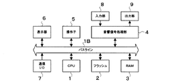
図1は、この発明に係る音響信号処理装置の電子的ハードウェア構成例を示すブロック図である。音響信号処理装置は、電子楽器、音源装置、エフェクタ、あるいはオーディオミキサなど、符号化された楽音信号又は音響信号を処理する装置である。なお、この明細書では所定のサンプリング周期で標本化され符号化された楽音信号又は音響信号を「波形データ」という。 FIG. 1 is a block diagram showing an example of an electronic hardware configuration of an acoustic signal processing apparatus according to the present invention. The acoustic signal processing device is a device that processes an encoded musical sound signal or acoustic signal, such as an electronic musical instrument, a sound source device, an effector, or an audio mixer. In this specification, a musical tone signal or an acoustic signal sampled and encoded at a predetermined sampling period is referred to as “waveform data”.
図1において、音響信号処理装置は、CPU1、フラッシュメモリ2、RAM3、音響信号処理部4、操作子5、表示器6、および通信インターフェース(通信I/F)7を含んで構成され、各部がデータおよびアドレスバス1Bを介して接続される。CPU1、フラッシュメモリ2、およびRAM3は音響信号処理装置の動作を制御する制御部である。フラッシュメモリ2にはCPU1が実行する各種プログラムを記憶されている。CPU1は、フラッシュメモリ2に記憶されたプログラムをRAM3に読み出し、該読み出したプログラムを実行する。
In FIG. 1, the acoustic signal processing apparatus includes a
操作子5は、各種パラメータの値や各種指示を入力するためのパネル操作子などである。音響信号処理装置が電子楽器の場合には、操作子5には、ユーザが演奏情報を入力するため演奏操作子(鍵盤など)も含まれる。表示器6は、例えば液晶ディスプレイによって構成され、CPU1の制御に基づき各種情報を表示する。また、音響信号処理装置は、通信I/O7を介して外部の装置とデータ通信可能に接続される。通信I/O7は、例えばMIDI規格の信号を送受信するためのMIDI I/Fや、あるいはEthernet(登録商標)規格の通信I/Fなど、従来から知られる適宜の規格の通信I/Fにより構成される。
The
音響信号処理部4は、波形データを入力する入力部8と、波形データを出力する出力部9とに接続されており、例えば楽音信号生成処理や、波形データに対する信号処理(音特性制御処理やミキシング処理)など、CPU1から与えられた指示に応じた処理を実行する。例えば、音響信号処理部4で楽音信号生成処理を行うときには、音響信号処理部4は、所定のサンプリング周期毎に波形データのサンプルを生成して、生成した波形データのサンプルを出力部9から出力する処理を行う。また、音響信号処理部4で音特性制御処理など波形データに対する信号処理を行うときには、所定のサンプリング周期毎に、入力部8から入力される波形データのサンプルを処理して、該処理結果の波形データのサンプルを出力部9から出力する処理を行う。音響信号処理部4において、波形データのサンプルを処理するサンプリング周期は“ワードクロック”によって与えられる。“ワードクロック”は、波形データのサンプルを処理するサンプリング周期を示す信号である。音響信号処理部4は、ワードクロックに同期した波形データのサンプルを処理する。ワードクロックを生成する構成など、ワードクロックの詳細については、後述する。
The acoustic
音響信号処理部4は、互いにシリアル接続された複数の集積回路(LSI:「Large Scale Integrated circuit」の略語)により構成されている。互いにシリアル接続された複数のLSIの間では、波形データのサンプルを双方向にシリアル伝送することができる。なお、波形データのシリアル伝送は、波形データの各サンプルを構成するビットデータ列を、シリアル伝送クロックの1クロックあたり1ビットずつ順次伝送する方法である。周知の通り、複数LSIで波形データのサンプルをシリアル伝送する場合には、各LSIを、ワードクロックを使ってサンプリング周期を同期させなければならない。この発明は、後述する通り、複数LSIでワードクロック同期するときに従来発生していた波形データの品質の劣化という問題を防止する点に特徴がある。
The acoustic
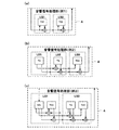
図2(a)〜(c)は、音響信号処理部4を構成する複数のLSIの接続例、および波形データの処理内容の具体例を説明する図である。(a)には、2つの音特性制御用のLSI1とLSI2とをシリアル接続した例を示す。図に示す文字列「TCC」は「Tone Characteristic Controller」の略、すなわち「音特性制御部」である。音特性制御部は、例えばイコライザ、コンプレッサ、あるいはリバーブなど、波形データに対してエフェクトを付与する処理を実行する。入力部8から入力された波形データはLSI1に入力され、該LSI1による信号処理結果がLSI2に出力される。該LSI1において、入力された波形データは、音特性制御部(TCC)に入り、その処理結果と音特性制御を施さない波形データとが合算されて、LSI2に出力される。LSI2おいても同様に、LSI1からシリアル伝送された波形データは、音特性制御部(TCC)に入り、その処理結果と音特性制御を施さない波形データとが合算されて、出力部9へ出力される。このように、音特性制御用の2つのLSIがシリアル接続されることで、音響信号処理部4は、音特性制御用のLSIを1つしか備えない構成に比較して、2倍の処理能力を持つ音特性制御回路となる。
2A to 2C are diagrams for explaining a connection example of a plurality of LSIs constituting the acoustic
また、(b)には、2つの楽音信号生成用のLSI1とLSI2と、1つの音特性制御用のLSI3との3つのLSIをシリアル接続した例を示す。図において「TG」は「Tone Generator」の略、すなわち「楽音信号生成部(音源)」を意味する。楽音信号生成部には、例えば、PCM音源、FM音源、あるいはアナログモデリング音源など、従来から知られる適宜の音源方式を適用してよい。LSI1とLSI2とは、それぞれサンプリング周期毎に複数時分割チャンネル動作を行い、CPU1の制御の下で、複数チャンネルの波形データのサンプルを同時に生成する。LSI1で生成した複数発音チャンネルの波形データは合算され、該合算結果の波形データはLSI2にシリアル伝送され、該LSI2において当該LSI2で生成された複数発音チャンネルの波形データと合算され、該合算結果の波形データが音特性制御用のLSI3にシリアル伝送される。ここで、LSI1とLSI2とはそれぞれ、LSI3の音特性制御部(TCC)を通る信号処理チャンネルと、該音特性制御をスルーする信号処理チャンネルとの2系統の信号処理チャンネルが用意されており、発音チャンネル毎に、生成された波形データを音特性制御部(TCC)に送るか、又は送らないかを制御することができる。このように、楽音信号生成用の2つのLSIと、音特性制御用の1つのLSIをシリアル接続することで、音響信号処理部4は、LSIを1つしか備えない構成に比較して2倍の発音数を持つ楽音発生回路として機能し、且つ、楽音発生回路で生成した波形データに対する音特性制御回路として機能する。ここでは、波形データの合算を1系統で行うようになっていたが、混合レベルを変えて複数系統で個別に合算し、LSI3で系統毎に異なる音特性制御をおこなうようにしてもよい。なお、(b)の構成の場合、図1の入力部8は不要である。
Further, (b) shows an example in which three LSIs of two musical sound
また、(c)は、音量レベル制御部(Vol)と音特性制御部(TCC)との2つの機能を担うLSI1と、楽音信号生成部(TG)と音特性制御部(TCC)との2つの機能を担うLSI2をシリアル接続した例を示す。図の例では、入力部8からLSI1に入力された波形データは音量レベル制御部に入力され、音量レベル制御部は制御結果を3系統の系統毎に個別にレベル制御を行い出力する。音量レベル制御部の3系統の出力のうちの1つは音特性制御部に入力され、音量レベル制御部の3つの出力のうちの別の1つはそのままLSI2に出力される。音量レベル制御部のさらに別の1つの出力は、音特性制御部の出力と合算されて、LSI2に出力される。また、LSI2の楽音信号生成部は、生成した複数チャンネルの波形データをそれぞれ3系統の系統別にレベル制御して合算し、3系統の合算結果をパラレルで出力する。LSI2の楽音信号生成部の3系統の出力のうちの1つは、LSI1の音特性制御部へ供給される。また、別の1つは、LSI1の音量レベル制御部の出力と合算され、LSI2の音特性制御部へ供給される。また、さらに別の1つは、LSI1の音量レベル制御部の出力とLSI1の音特性制御部の出力との合算結果に合算され、その合算結果がLSI2の音特性制御部と合算され、音響信号処理部4の最終的な出力として、出力部8へ供給されるよう結線されている。このような構成によれば、LSI1およびLSI2の各ステージを自由に結線することができ、例えば、LSI2の楽音信号生成部が生成した波形データをLSI1の音特性制御部で処理する等の、自由度の高い音響信号処理を行うことができる。
(C) is an
図2(a)〜(c)に例示したように、複数のLSIをシリアル接続することで、音響信号処理部4の能力が拡張される。音響信号処理部4を構成するLSIの数は限定されない。全体として所望の性能の音響処理部4になるよう、複数のLSIを順次シリアル接続することができる。
As illustrated in FIGS. 2A to 2C, the capability of the acoustic
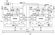
図3は、音響信号処理部4のハードウェア構成の詳細を示すブロック図である。図3に示す音響信号処理部4において、第1LSI(「LSI1」)10と第2LSI(「LSI2」)20との2つのLSIがシリアル接続される。図3の例では、符号10の「LSI1」がワードクロックのマスタLSIであり、符号20の「LSI2」がワードクロックのスレーブLSIである。すなわち、マスタLSI10からスレーブLSI20にワードクロック(図3において「Wクロック」)を供給することで、該供給されたワードクロックにスレーブLSIのワードクロック(波形データを処理するサンプリング周期)を同期させる。
なお、この発明に係る実施例において、LSI10、およびLSI20は、それぞれ、ワードクロックの1クロックに対する動作クロックのクロック数が固定値で設計されたLSIとする。この実施例においては、一例としてワードクロックの1クロックに対する動作クロックのクロック数が「4096」クロックに固定されているものとする。また、サンプリング周期は、48kHzとする。
FIG. 3 is a block diagram showing details of the hardware configuration of the acoustic
In the embodiment according to the present invention, each of the
マスタLSI(「LSI1」)10は、処理回路11、第1シリアルインターフェース(シリアルI/O)12、第2シリアルI/O13、動作クロック発生器(O_CLK発生器:「O_CLK」はOperation Clockの略)14、動作カウンタ15、および制御レジスタ16を備える。また、スレーブLSI(「LSI2」)20は、処理回路21、第1シリアルI/O22、第2シリアルI/O23、動作クロック発生器24、動作カウンタ25、制御レジスタ26、およびリセットタイミング補正部(RT補正:「RT」は「Reset Timing」の略)27を備える。図3の例では、マスタLSI10とスレーブLSI20の構成上の違いは、スレーブLSI20が、RT補正部27を備える点である。
The master LSI (“
LSI10,20に備わる制御レジスタ16,26は、バス1Bを介してCPU1に接続されており、該CPU1から与えられるLSI10,20の各部の制御パラメータの値や、処理回路11,21が実行するマイクロプログラム等を格納するレジスタである。処理回路11,21は、音特性制御用のLSIであれば、CPU1によりレジスタに設定されたマイクロプログラムを実行して、レジスタに設定されたアドレスや係数のパラメータを用いて、デジタル信号(波形データ)に対する信号処理を行う回路(DSP:digital signal processorの略)であって、波形データに対する音特性制御等の信号処理(エフェクタ機能)を実行する。また、楽音信号生成用のLSIであれば、各発音チャンネル毎に、CPU1からの発音指示に応じて、レジスタに設定された当該発音チャンネルの楽音制御パラメータに応じた波形データの生成処理を行う回路であって、該楽音制御パラメータに応じた楽音特性を有する波形データを生成する楽音信号生成処理(音源機能)を実行する。
The control registers 16 and 26 provided in the
LSI10のシリアルI/O12、13、およびLSI20のシリアルI/O22、23は、シリアル伝送方式により波形データを入出力するためのインターフェースである。図3に示す構成では、マスタLSI10が第1シリアルI/O12を介して波形データの入力部8(図1参照)に接続されており、該入力部8から入力された波形データはマスタLSI10にシリアル伝送され、処理回路11に供給される。また、マスタLSI10の第2シリアルI/O13とスレーブLSI20の第1シリアルI/O22とを介して、マスタLSI10とスレーブLSI20とがシリアル接続されており、該マスタLSI10とスレーブLSI20との間で波形データが双方向にシリアル伝送される。そして、スレーブLSI20が第2シリアルI/O23を介して波形データの出力部9(図1参照)に接続されており、該スレーブLSI20の処理回路21から出力された波形データは該出力部9へシリアル伝送され出力される。ここで、マスタLSIとスレーブLSIの間のシリアル伝送では、シリアル伝送クロックとして、後述する動作クロックから(分周により)直接生成されたクロックが使用される。
The serial I /
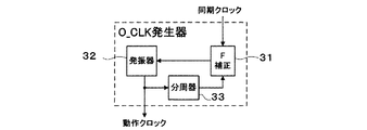
マスタLSI10の動作クロック発生器14、およびスレーブLSI20の動作クロック発生器24は、それぞれ、同期クロック発生器(S_CLK発生器:「S_CLK」はSynchronization Clockの略)30に接続されている。同期クロック発生器30は、マスタLSI10およびスレーブLSI20のそれぞれの動作クロックよりも周波数の低い、例えば約6MHzの、同期クロックを発生し、マスタLSI10とスレーブLSI20とのそれぞれに、同じ同期クロックを供給する。同期クロック発生器30が発生する同期クロックとは、マスタLSI10の動作クロック発生器14、およびスレーブLSI20の動作クロック発生器24のそれぞれで同期した動作クロックを発生するために利用されるクロックである。
The
マスタLSI10の動作クロック発生器14、およびスレーブLSI20の動作クロック発生器24は、同期クロック発生器30から供給された同期クロックを、例えば32逓倍することにより、該同期クロックよりも周波数の高い、例えば、200MHzの、動作クロックを発生する。動作クロック発生器14,24の詳細な構成例を、図4に示す。図4に示す通り、動作クロック発生器は、同期クロック発生器30から供給された同期クロックとフィードバック信号との位相差を検出する周波数補正部(F補正:「F」はfrequencyの略)31と、該周波数補正部31の出力信号により発振周波数が制御される発振器31と、発振器31の出力と周波数補正部31の入力の間に挿入された分周器32とから構成される。周波数補正部31は、同期クロック発生器30から供給された同期クロックと分周器32を介してフィードバックされた発振器32の出力信号との位相差を検出し、該位相差に応じた出力信号を発振器32に出力することで、同期クロックの位相に対して発振器32の出力信号の位相が一定の関係を保つように、発振器32の発振周波数を制御(補正)する。ここで分周器32を介してフィードバックされる発振器32の出力信号は、発振器32の出力周波数を所定の分周比N(Nは任意の整数)で分周したものである。したがって、発振器32は、同期クロックに同期した動作クロックであって、該同期クロックをN倍逓倍した周波数の動作クロックを出力する。すなわち、動作クロック発生器は、PLL(Phase Locked Loop:「位相ロックループ」の略)による周波数逓倍器である。
The
マスタLSI10の動作クロック発生器14で生成された動作クロックは、自身の処理回路11と、第1及び第2シリアルI/O12,13に供給されるとともに、動作カウンタ15に供給される。処理回路11と、第1及び第2シリアルI/O12,13は、動作クロック発生器14で生成された動作クロックに基づき動作する。
The operation clock generated by the
マスタLSI10の動作カウンタ15は、動作クロック発生器14から供給された動作クロックをカウントし、所定カウント値ごとに1クロックのレートでワードクロックを生成する。ワードクロックは波形データのサンプリング周期を示す。この実施例では、動作カウンタ15は、例えば12ビットのカウンタであり、その下限値「0」から上限値「4095」までのカウント期間が、ワードクロックの1クロックの期間に相当する。すなわち、カウント値の最上位ビットに現れる信号が動作カウンタ15で生成されるワードクロックである。サンプリング周期毎にカウントされる総クロック数「4096」は、ワードクロックの1クロックに対応する所定カウント数である。動作カウンタ15は、フリーランで、下限値「0」から上限値「4095」までカウントすることを繰り返すものである。そして、ワードクロックのタイミングは、ワードクロックの値が「1」から「0」に変化するタイミング、つまり、カウント値が「4095」から「0」に戻るタイミングを言う。マスタLSI10の動作カウンタ15が生成したワードクロックは、ワードクロックとしてスレーブLSI20に供給されるとともに、自身の処理回路11と、第1及び第2シリアルI/O12,13とに供給される。
The operation counter 15 of the
処理回路11と、第1及び第2シリアルI/O12,13は、動作カウンタ15のカウント値に基づき、前記ワードクロックに同期した波形データのサンプルを処理する。第1及び第2シリアルI/O12,13は、動作クロックを例えば80分周することにより、約2.5MHzのシリアル伝送クロックを生成し、生成したシリアル伝送クロックの1クロック毎に、波形データのサンプルを構成するビット列を1ビットずつ順次伝送することで、動作カウンタ15で生成されたワードクロックに同期して、波形データのサンプルの入出力を行う。なお、シリアル伝送クロックは、動作クロック発生器14で発生した動作クロックに基づき生成されるものである。また、処理回路11は、該カウント値により実行すべき処理内容(例えば、マイクロプログラムのステップ番号)が決定され、動作カウンタ15で生成されたワードクロックに同期して、波形データのサンプル毎の処理(楽音生成や、音特性制御など)を行う。
The processing circuit 11 and the first and second serial I /
スレーブLSI20の動作クロック発生器24で生成された動作クロックは、自身の処理回路21と、第1及び第2シリアルI/O22,23に供給されるとともに、動作カウンタ25に供給される。スレーブLSI20の動作カウンタ25は、動作クロック発生器14から供給された動作クロックをカウントする。動作カウンタ25のカウント上限値は、ワードクロックの1クロックの周期に相当する値(この実施例では一例として「4095」)である。動作カウンタ25は、動作クロックのクロック数を、下限値「0」から上限値「4095」までカウントすることを繰り返すものである。動作カウンタ25のカウント値は、自身の処理回路21、第1及び第2シアルI/O22,23、およびRT補正部27に供給される。スレーブLSI20内の各部に対する動作クロックおよび動作カウンタ25のカウント値の働きは、マスタLSI10のそれと同様である。つまりスレーブLSI20内の各部で波形データを処理するサンプリング周期は、動作カウンタ25のカウント値によって与えられる。スレーブLSI20は、動作カウンタ25のカウント開始タイミング(下限値「0」のタイミング)が、マスタLSI10から供給されるワードクロックのタイミングから大きくずれないように制御されている点がマスタLSI10と異なる。動作カウンタ25のカウント開始タイミングを、マスタLSI10の動作カウンタ15のカウント開始タイミングとほぼ同じにすることにより、スレーブLSI20においてマスタLSI10のシリアル伝送クロックとほぼ同じタイミングのシリアル伝送クロックを生成して、スレーブLSI20とマスタLSI10の間でシリアル伝送が行えるようになる。
The operation clock generated by the
スレーブLSI20の動作カウンタ25のカウントタイミングとマスタLSI10の動作カウンタ15のカウントタイミングとがずれたときに、その両カウンタのカウントタイミングを同期化させる手法は、基本的には、ワードクロックがスレーブLSI20に入力されたタイミングで、動作カウンタ25のカウント値をリセットする、従来技術の「リセット型」相当の手法である。この発明は、RT補正部27により、多少カウントタイミングがずれても動作カウンタ25のリセットを行わず、特定の条件が満たされた場合のみ動作カウンタ25のリセットを行うようにした点に特徴がある。
When the count timing of the
RT補正部27は、マスタLSI10からのワードクロックのタイミングで動作カウンタ25のカウント値を見ることにより、動作カウンタ25のカウントタイミングと動作カウンタ15のカウントタイミングのずれを検出して、そのずれが所定の閾値以上となったときにだけ、動作カウンタ25のカウント値をリセットするものである。動作カウンタのリセットを行う点こそ従来技術の「リセット型」と同じだが、ここでのリセットの目的は、動作カウンタ25のカウント周期をマスタLSI10に合わせることではなく、そのカウントタイミングをマスタLSI10に合わせることにある。「ワードクロックのタイミングにおける動作カウンタ25のカウント値」は、その最上位ビット(第12ビット)を符号ビットと解釈すれば、最小値「−2048」から最大値「+2047」までの、動作カウンタ15に対する動作カウンタ25のカウントタイミングずれを示す「ずれカウント値」となる。該ずれカウント値は、動作カウンタ25のカウントタイミング(カウント値の位相)が動作カウンタ15より早い場合は正となり、遅い場合は負となる。また、該ずれカウント値の絶対値は、カウントタイミング(カウント値の位相)のずれの大きさに対応する。
The
この実施例では、RT補正部27は、制御レジスタ26に設定された動作モードパラメータの値に応じた動作モードで動作するものとする。RT補正部27の動作モードには、動作カウンタ25の動作をマスタLSI10から供給されるワードクロックに常時同期させる「モード1」と、マスタLSI10からのワードクロックのタイミングにおける動作カウンタ25のカウント値(位相のずれに位相)が、所定の閾値以上となったときに同期をかける「モード2」と、動作カウンタ25の動作をマスタLSI10から供給されるワードクロックに同期させない「モード0」との三通りのモードがある。「モード2」の動作が、RT補正部27に特徴的な動作である。
In this embodiment, it is assumed that the
「モード2」の場合、RT補正部27には制御レジスタ26に格納された所定の閾値が設定される。そして、RT補正部27は、マスタLSI10からのワードクロックのタイミングにおける動作カウンタ25のカウント値(位相のずれに位相)が、所定の閾値以上となったときに、そのタイミングで動作カウンタ25のカウント値をリセットする。ここで、RT補正部27に設定される閾値は、マスタLSI10とスレーブLSI20の間のデータのシリアル伝送で許容できる各ビットデータの時間ずれに応じて予め設定された値であって、その具体的な値はシリアル伝送の仕様に応じて適宜の値に設定される。
In “
したがって、RT補正部27が「モード2」で動作しているときには、マスタLSI10からのワードクロックのタイミングにおける動作カウンタ25のカウント値(位相のずれに相当)が、前記閾値に達するまでは、該マスタLSI10から供給されたワードクロックに応じた動作カウンタ25のカウント値のリセットが行われない。すなわち、ワードクロックの入力タイミングに対する第2動作クロックカウンタ部のリセットタイミングに閾値分だけマージンを確保して、該閾値分のずれの範囲ならば、動作カウンタ25のカウント周期とマスタLSI10から供給されるワードクロックとの同期がとれているものと見なす。
Therefore, when the
また、「モード1」の場合、マスタLSI10からRT補正部27にワードクロックが入力される毎に、RT補正部27は動作カウンタ25のカウント値をリセットする。よって、RT補正部27が「モード1」で動作しているときには、マスタLSI10から供給されるワードクロックの1クロックが入る毎に、動作カウンタ25のカウント値がリセットされる。したがって、動作カウンタ25のリセットタイミングは、マスタLSI10から供給されるワードクロックに常時同期する。これは従来のスレーブLSIの「リセット型」ワードクロック同期方法と同じ動作である。
In the case of “
また、「モード0」は、マスタLSI10からRT補正部27にワードクロックが入力されても、動作カウンタ25にリセットをかけない動作モードである。つまり、動作カウンタ25のカウント周期とマスタLSI10から供給されるワードクロックの同期をとらない。これは、LSI20を単独又はワードクロックマスタとして使うときの動作カウンタの使い方であるから、スレーブLSIではRT補正部27に「モード0」を設定することはない。
“Mode 0” is an operation mode in which the
図3の例では、音響信号処理部4を構成するマスタLSI10とスレーブLSI20とがそれぞれ異なる構成(スレーブLSI20にのみRT補正部27が備わる構成)を示したが、2つのLSI10,20は、それぞれ、マスタLSIとスレーブLSIとのいずれの働きも可能な同一構成のLSIで構成されてもよい。図5は、マスタLSIとスレーブLSIとのいずれの働きも可能なLSIの構成例を示す。図5に示す通り、LSI40は、処理回路41、第1シリアルI/O42、第2シリアルI/O43、動作クロック発生器44、動作カウンタ45、制御レジスタ46、およびRT補正部47を備える。LSI40を、マスタLSIとして機能させるときには、RT補正部47に動作モードパラメータとして「モード0」を設定することで、動作カウンタ45の動作を外部のクロックに同期させない。また、動作カウンタ45でカウントした動作クロックのカウント値に基づくワードクロックをスレーブLSIに出力する。一方、LSI40を、スレーブLSIとして機能させるときには、RT補正部47に動作モードパラメータとして「モード1」又は「モード2」を設定して、外部(マスタLSI)から供給されたワードクロックに動作カウンタ45のカウント周期を同期させる。
In the example of FIG. 3, the
図6は、図1の音響信号処理装置を制御するためにCPU1が実行するメイン処理の手順の一例を示すフローチャートである。音響信号処理装置の起動時に、CPU1は、音響信号処理部4の初期設定処理を行い(ステップS1)、また、音響信号処理部4以外のその他の各部の初期設定を行う(ステップS2)。図7は、前記ステップS1においてCPU1が実行する音響信号処理部4の初期設定処理の手順の一例を示すフローチャートである。図7のステップS6において、CPU1は、スレーブLSI20の制御レジスタ26にRT補正部27の動作モードパラメータの値として「モード1」をセットする処理を行う。なお、マスタLSIがRT補正部を備える構成(図5の構成)の場合には、当該ステップS6においてマスタLSIの制御レジスタ(図5において符号46)にRT補正部の動作モードパラメータの値として「モード0」をセットする。マスタLSIが図3に示すようにRT補正部を備えない構成であれば、当該ステップS6でのマスタLSIに関するモード設定は不要である。
FIG. 6 is a flowchart showing an example of a procedure of main processing executed by the
上記ステップS6によりスレーブLSI20のRT補正部27は「モード1」で動作するよう設定される。したがって、音響信号処理装置の起動時には、スレーブLSI20の動作カウンタ25のカウント周期はマスタLSI10から供給されるワードクロックに常時同期する状態になる。一方、マスタLSI10は、外部からのクロックに同期することなく、動作カウンタ(図3において符号15)で動作クロックを自身のカウントし、そのカウント値に基づくワードクロックをスレーブLSI20に供給可能な状態になる。
In step S6, the
ステップS7において、CPU1は、マスタLSI10からスレーブLSI20にワードクロックが供給されるのを待つ。前記ステップS6によりスレーブLSI20のRT補正部27の動作モードに「モード1」が設定されているので、マスタLSI10からスレーブLSI20にワードクロックが供給されると、スレーブLSI20のRT補正部27は、マスタLSI10からワードクロックが入力されたタイミングで動作カウンタ25のカウント値をリセットする。これにより、スレーブLSI20とマスタLSI10のワードクロック位相の同期(動作カウンタ15と動作カウンタ25のカウントタイミングの同期)が行われる。ワードクロックは、サンプリング周期で入力(変化)するので、ステップS7では、最低1サンプリング周期相当の期間だけ待てばよい。
In step S <b> 7, the
ステップS8において、CPU1は、スレーブLSI20の制御レジスタ26に、RT補正部27の動作モードのパラメータの値として「モード2」をセットするとともに、RT補正部27に設定される閾値をセットする。これにより、スレーブLSI20は、マスタLSI10からワードクロックが供給されたタイミングにおける動作カウンタ25のカウント値と、ワードクロックの1クロックに対応する動作クロックのクロック数との差が前記閾値に達するまでは、該マスタLSI10から供給されたワードクロックに応じた動作カウンタ25のリセットが行われないよう設定される。そして、ステップS9において、CPU1は、マスタLSI10の制御レジスタ16とスレーブLSI20の制御レジスタ26とのそれぞれに所定の初期データを設定する。ここで設定される初期データは、例えばLSIが楽音生成部(音源)であれば、全ての発音チャンネルに対する発音オフを指示するデータなどであり、また、例えばLSIが音特性制御部(エフェクタ)であれば、波形データの出力ミュートを指示するデータなどである。
In step S <b> 8, the
図6に戻ると、CPU1は、上記ステップS1およびステップS2において初期設定を行った後、音響信号処理装置のメイン動作を行う。すなわち、CPU1は、操作子5の操作に応じた操作データの入力や入力部8からの波形データの入力など、何らかのイベントを検出し(ステップS3)、イベントを検出したら(ステップS4のYES)、該検出したイベントに応じた処理を実行する(ステップS5)。前記ステップS5において実行される処理は、具体的には、例えば、音響信号処理部4(マスタLSI10,スレーブLSI20)が1ないし複数の楽音信号生成部(TG)を含む場合には、発音を支持するイベント(ノートオン)に応じて、何れかの発音チャンネルを割り当て、レジスタに割り当てた発音チャンネルの楽音制御パラメータを設定し、同発音チャンネルに波形データの生成を開始させる処理や、音量を指示するイベント(エクスプレッション)に応じて、波形データを生成している発音チャンネルの音量パラメータの値を変更し、該波形データの音量を変化させる処理などである。また、音響信号処理部4が音特性制御部(TCC)を含む場合には、エフェクトを選択するイベントに応じて、レジスタにその選択されたエフェクトのマイクロプログラム、アドレス、係数などを設定することにより、選択されたエフェクトの信号処理を実行させる処理や、該エフェクトのパラメータを変更するイベントに応じて、レジスタのアドレスないし係数の値を変更する処理などである。
Returning to FIG. 6, the
音響信号処理装置のメイン動作における、マスタLSI10とスレーブLSI20とのワードクロック同期(マスタLSI10のワードクロックと動作カウンタ25のカウント周期の同期)の動作について説明する。マスタLSI10とスレーブLSI20には、それぞれ、S_CLK発生器30から出力された同期クロックが供給される。マスタLSI10の動作クロック発生器14と、スレーブLSI20の動作クロック発生器24は、それぞれ、その同期クロックに同期した動作クロックを発生する。マスタLSI10は、動作カウンタ15において動作クロック発生器14で発生した動作クロックをカウントし、該動作カウンタ15のカウント値に同期したタイミングで該ワードクロックに同期した波形データのサンプルを処理する一方で、そのカウント値の最上位ビットであるワードクロックをスレーブLSI20に供給する。
The operation of the word clock synchronization (synchronization of the word clock of the
スレーブLSI20の動作カウンタ25は、動作クロック発生器24発生した動作クロックをカウントする。スレーブLSI20のRT補正部27は、前記ステップS8により「モード2」で動作するよう設定されているので、マスタLSI10からのワードクロックのタイミングにおける動作カウンタ25のカウント値(位相ずれに相当)が、前記閾値に達するまでは、該マスタLSI10から供給されたワードクロックに応じた動作カウンタ25のカウント値のリセットが行われない。そして、マスタLSI10からのワードクロックのタイミングにおける動作カウンタ25のカウント値(位相ずれに相当)が、前記閾値を越えたときに、RT補正部27は動作カウンタ25をリセットして、スレーブLSI20の動作カウンタ25のカウントタイミングをマスタLSI10の動作カウンタ15のカウントタイミングに一致させる。
The operation counter 25 of the
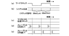
図8は、RT補正部27の閾値、すなわち、マスタLSI10からワードクロックが供給されたタイミングにおける動作カウンタ25のカウント値と、ワードクロックの1クロックに対応する動作クロックのクロック数とのずれとして許容する範囲を説明するためのタイミングチャートである。閾値は、LSI10,20の間のデータのシリアル伝送の仕様、具体的にはワードクロックに対する各ビットデータの時間ずれの許容限度に基づき決定される。図8において(a)は1クロック(1周期)のワードクロックである。例えば、シリアル伝送の仕様の一例として、上述したように、マスタLSI10およびスレーブLSI20の動作クロックを200MHz程度、LSI間のシリアル伝送クロックを約2.5MHzであり、シリアル伝送クロックの1クロックに対する動作クロックのクロック数が80であるとする。(b)はワードクロックの1クロックで波形データのサンプルがシリアル伝送される様子を示す。上記仕様のシリアル伝送では、LチャンネルおよびRチャンネルの2チャンネルステレオ波形データ(ステレオ信号)のサンプルをそれぞれ20ビットずつシリアル伝送する(最大26ビットずつ伝送可能)。また(b)に示す通り、ワードクロックの半周期以内にステレオ信号の1チャンネル分のデータが伝送されるようになっており、ワードクロックの立ち上がり及び立ち下がりのタイミングが各チャンネルのデータの先頭を示している。
FIG. 8 shows an allowable difference between the threshold value of the
シリアル伝送の仕様の一例として、シリアル伝送における各ビットデータの時間ずれの許容限度を25%とすると、図8(c)に示すマスタLSI10のシリアル伝送クロックに対して、スレーブLSI10のデータ伝送タイミングに25%進んだ時間ずれがある場合、(d)に示すように、スレーブLSI20では、波形データのサンプルの伝送開始タイミングはワードクロックの立ち上がりと立下りに対して25%分早くなる。反対に、25%遅れた時間ずれがある場合、(e)に示すように、スレーブLSI20では、波形データのサンプルの伝送開始タイミングはワードクロックの立ち上がりと立下りに対して25%分遅くなる。いずれにせよ、許容限度の範囲内ならば、マスタLSI10とスレーブLSI20との間で波形データのシリアル伝送は行うことができる。シリアル伝送における各ビットデータの時間ずれを動作クロックで表現すると、ここで述べている例ではシリアル伝送クロックの1クロックに対する動作クロックのクロック数を80としているので、シリアル伝送における各ビットデータの25%の時間ずれは、動作クロックの20クロック分に相当する。従って、(d)及び(c)に示された時間ずれは、それぞれワードクロックのタイミングに対するスレーブLSIの動作クロックの20クロック分の進み又は遅れに相当する。なお、図8(c)、(d)及び(e)の時間軸は、(a)及び(b)の時間軸を約50倍に拡大したものとなっている。
As an example of the serial transmission specification, if the allowable limit of the time lag of each bit data in serial transmission is 25%, the data transmission timing of the
よって、シリアル伝送における各ビットデータの時間ずれ許容限度(25%)に対応する動作クロックのクロック数「20クロック」を、RT補正部27の閾値に設定することことにより、この実施例のようにワードクロックの1クロックに対する動作クロックのクロック数を「4096」とする場合には、ずれカウント値の上限値は「+20」(カウント値の「20」に相当)、下限値は「−20」(カウント値の「4076」に相当)となる。動作カウンタ25のカウント値の位相と動作カウンタ15のカウント値の位相ずれを閾値分だけ許容し、該閾値分のずれの範囲ならば、動作カウンタ25のカウント周期とマスタLSI10から供給されるワードクロックとの同期がとれているものと見なす。これにより、マスタLSI10からのワードクロックのタイミングにおける動作カウンタ25のカウント値が「4076」〜「4095」又は「0」〜「20」の範囲(ずれカウント値の「−20」〜「+20」の範囲に相当)内であれば、ワードクロックのタイミングに応じた動作カウンタ25のリセットを行わないようになり、動作カウンタ25のリセットによって生じる波形データの品質劣化を防止することができる。そして、RT補正部27は、マスタLSI10からのワードクロックのタイミングにおける動作カウンタ25のカウント値が、「21」〜「4075」の範囲(ずれカウント値の「−21」以下又は「+21」以上の範囲に相当)であれば、マスタLSI10からのワードクロックのタイミングで動作カウンタ25のカウント値をリセットすることで、動作カウンタ25のカウント値の位相をマスタLSI10の動作カウンタ15のカウント値の位相に合わせる。
Therefore, by setting the clock number “20 clocks” of the operation clock corresponding to the time shift allowable limit (25%) of each bit data in the serial transmission to the threshold value of the
このように本実施例によれば、スレーブLSI20にRT補正部27を設けることにより、マスタLSI10からのワードクロックのタイミングにおける動作カウンタ25のカウント値(位相ずれに相当)が、閾値に応じた範囲から外れるときだけ、ワードクロックのタイミングに動作カウンタ25をリセットする、つまり、スレーブLSI20の動作カウンタ25のカウント値の位相と、マスタLSI10の動作カウンタ15のカウント値の位相との差が、閾値を越えない限り動作カウンタ25をリセットしないよう構成することで、LSI間のシリアル伝送の信頼性を確保しつつ、動作カウンタ25のリセットによって生じる波形データの品質が劣化することを防止することができる。
As described above, according to the present embodiment, by providing the
マスタLSI10の動作クロックもスレーブLSI20の動作クロックも、互いに同じ同期クロックに同期しているクロックであるから、理想的には、マスタLSI10とスレーブLSI20とは同じ動作クロックで動作する。しかし、実際には、動作クロック発生器14、24において同期クロックを逓倍してそれぞれの動作クロックを生成していることから、マスタLSI10とスレーブLSI20との動作クロックの間には「わずかな周波数ずれ」が生じる。そして、このスタLSI10とスレーブLSI20との動作クロックの間の「わずかな周波数ずれ」のために、動作カウンタ15のカウント値と動作カウンタ25のカウント値の間には位相差が生じる。しかし、マスタLSI10の動作クロックもスレーブLSI20の動作クロックも、同じ同期クロックに同期しているクロックであるから、それだけの要因であれば、その位相差は、それ程大きくなることはなく、RT補正部27による動作カウンタ25のリセットは起こらない。より大きな位相差が生じるそれ以外の要因としては、例えば突発的なノイズ、信号の飛びつき、電磁波などが考えられる。これら要因により、動作カウンタ15のカウント値と動作カウンタ25のカウント値の間に閾値以上の位相差が生じた場合は、RT補正部27が、ワードクロックのタイミングで動作カウンタ25をリセットし、その位相差を解消する。しかしながら、このような要因が生じることは極めて希である。よって、本発明の音響信号処理装置によれば、動作カウンタ25のリセットによって波形データが品質劣化することを、実質的になくすることができる。
Since the operation clock of the
なお、前記図3の音響信号処理部4は、シリアル接続された2つのLSI10,20のうちで、波形データの入力部8に接続されたLSI10をワードクロックのマスタLSIとし、出力部9に接続されたLSI20をワードクロックのスレーブLSIとする接続例を示したが、図9(a)のように、シリアル接続された2つのLSI48,49のうちで、波形データの入力部8に接続されたLSI48をワードクロックのスレーブLSIとし、波形データの出力部9に接続されたLSI49をワードクロックのマスタLSIとすることもできる。つまり、マスタLSIは、図3のように波形データの経路の上流にあってもよいし、図9(a)のように波形データの経路の下流にあってもよい。
The acoustic
また、3つ以上のLSIをシリアル接続した場合は、複数のLSIのいずれか1つがマスタLSIとなり、残りがスレーブLSIとなる。図9(b)に3つ以上のLSIをシリアル接続した場合の接続例を示す。図9(b)においては、シリアルに接続された4つのLSI50、51、52、および53のうち、LSI51がマスタLSIとなり、スレーブLSI50、52、および53にワードクロックを供給する。この場合、スレーブLSI50、及び52とマスタLSI51とのシリアル伝送は、前述の2つのLSIをシリアル接続する接続例と同様にマスタLSIとスレーブLSIとの間のシリアル伝送であるが、スレーブLSI52とスレーブLSI53との間では、スレーブLSI同士で波形データのシリアル伝送を行う。このようにスレーブLSI同士で波形データをシリアル伝送する場合には、マスタLSIと直接波形データをシリアル伝送する場合よりも、ワードクロックに対する各ビットデータの時間ずれの許容限度が狭くなるので、RT補正部に設定する閾値をマスタLSIとスレーブLSIとでシリアル伝送する場合の閾値の半分に設定する。すなわち、ワードクロックの1クロックに対する動作クロックのクロック数を4096、シリアル伝送における各ビットデータの時間ずれ許容限度が25%とすると、スレーブLSI同士で波形データをシリアル伝送する場合には、RT補正部に設定する閾値は動作クロックのクロック数「10クロック」である。その場合、マスタLSIからのワードクロックのタイミングにおける動作カウンタ25のカウント地位が、「4086」〜「4095」又は「0」〜「10」の範囲(ずれカウント値「−10」〜「+10」の範囲に相当)内にあれば、動作カウンタ25のリセットを行わない。このように、スレーブLSI同士で波形データをシリアル伝送する場合には、RT補正部に小さな閾値(1/2の閾値)を設定して、小さなずれで動作カウンタ25のリセットがかかるようにする。
When three or more LSIs are serially connected, any one of the plurality of LSIs becomes a master LSI, and the rest become slave LSIs. FIG. 9B shows a connection example when three or more LSIs are serially connected. In FIG. 9B, among the four
なお、上記実施例では、音響信号処理部4の初期設定処理として、図7のステップS6でRT補正部27の動作モードとして「モード1」をセットし、ワードクロックのタイミングと動作カウンタ25のカウント動作を同期させてから(ステップS7)、ステップS8においてRT補正部27の動作モードとして「モード2」モード2をセットするものとした。しかかし、この処理は、RT補正部27の動作モードを切り替える処理によって実現する方法に限らず、ステップS6においてRT補正部27の閾値として「0」をセットすることで実質的にモード1と同じ動作(常時同期)を行ってから、ステップS8で実質的な閾値、すなわちシリアル伝送における各ビットデータの時間ずれの許容限度に対応する値をセットするよう構成することもできる。また、この信号処理部4の初期設定のための制御は、上記実施例のようにCPU1の制御によって実行されるのではなく、スレーブLSIの起動時にRT補正部の閾値切り替え処理を含む初期設定用のマイクロプログラムをスレーブLSIに実行させることで、スレーブLSIで自動的に行ってもよい。
In the above embodiment, as the initial setting process of the acoustic
また、上記実施例では、各ワードクロックのタイミングで、カウントタイミングのずれを閾値と比較し、比較結果に応じてリセットを行うようになっていたが、比較とリセ宇ットとを異なるワードクロックのタイミグで行うようにしてもよい。例えば、あるワードクロックで、カウントタイミングのずれを閾値と比較し、その比較結果に応じて、次のワードクロックのタイミングでリセットを行うようにしてもよい。 In the above embodiment, the count timing deviation is compared with the threshold at each word clock timing, and reset is performed according to the comparison result. You may be made to perform in the timing. For example, the count timing shift may be compared with a threshold value using a certain word clock, and the reset may be performed at the next word clock timing according to the comparison result.
また、上記実施例におけるサンプリング周波数、同期クロック、動作クロック、シリアル伝送クロックの各周波数、動作クロック発生器14、24の逓倍数、およびシリアル伝送クロックを生成する際の分周比は、一例に過ぎず、それぞれ異なる値で設計できる。また、シリアル伝送における各ビットデータの時間ずれの許容限度も一例であり、シリアル伝送回路や動作条件によって異なる。
Further, the sampling frequency, the synchronization clock, the operation clock, the serial transmission clock frequency, the multiplication number of the
1 CPU、2 フラッシュメモリ、3 RAM、4 音響信号処理部、5 操作子、6 表示器、7 通信I/O、8 入力部、9 出力部、10 マスタLSI、11 処理回路、12,13 シリアルI/O、14 動作クロック発生器、15 動作カウンタ、16 制御レジスタ、20 スレーブLSI、21 処理回路、22,23 シリアルI/O、24 動作クロック発生器、25 動作カウンタ、26 制御レジスタ、27 リセットタイミング補正部、30 同期クロック発生器 1 CPU, 2 flash memory, 3 RAM, 4 acoustic signal processing unit, 5 operator, 6 display, 7 communication I / O, 8 input unit, 9 output unit, 10 master LSI, 11 processing circuit, 12, 13 serial I / O, 14 operation clock generator, 15 operation counter, 16 control register, 20 slave LSI, 21 processing circuit, 22, 23 serial I / O, 24 operation clock generator, 25 operation counter, 26 control register, 27 reset Timing correction unit, 30 synchronous clock generator
Claims (2)
前記複数の集積回路のうちの1つの集積回路は、
前記同期クロック生成部から出力された同期クロックを逓倍した第1動作クロックを生成する第1動作クロック生成部と、
前記第1動作クロックを分周して、第1ワードクロックを生成する第1ワードクロック生成部と、
前記第1動作クロックに基づいて、前記第1ワードクロックに同期した波形データの処理を行う第1信号処理部と、
前記複数の集積回路のうちの他の集積回路に接続され、該接続された他の集積回路との間で波形データをシリアル通信するための第1シリアル通信部と、
前記第1ワードクロックを前記複数の集積回路のうちの他の集積回路に出力するワードクロック出力部と
を備える第1集積回路であり、
前記複数の集積回路のうちの別の集積回路は、
前記同期クロック生成部から出力された同期クロックを逓倍した第2動作クロックを生成する第2動作クロック生成部と、
前記第2動作クロックを分周して、第2ワードクロックを生成する第2ワードクロック生成部と、
前記第1集積回路の前記ワードクロック出力部から出力された第1ワードクロックを入力するワードクロック入力部と、
前記ワードクロック入力部に第1ワードクロックと、前記第2ワードクロック生成部で生成した第2ワードクロックを位相比較して、その位相差が前記シリアル通信の伝送クロックの位相ずれの許容限度に対応した所定の閾値以上であるときに、前記第2ワードクロックの位相が前記第1ワードクロックの位相とほぼ同じになるよう、前記第2ワードクロック生成部の生成動作を制御する補正部と、
前記第2動作クロックに基づいて、前記第2ワードクロックに同期した波形データの処理を行う第2信号処理部と、
前記複数の集積回路のうちの他の集積回路に接続され、該接続された他の集積回路との間で波形データをシリアル通信するための第2シリアル通信部と
を備える第2集積回路である
ことを特徴とする音響信号処理装置。 In an acoustic signal processing device comprising two or more integrated circuits and a synchronous clock generation unit that generates a synchronous clock having a constant period and outputs the generated synchronous clock to each of the plurality of integrated circuits.
One integrated circuit of the plurality of integrated circuits is:
A first operation clock generation unit that generates a first operation clock obtained by multiplying the synchronization clock output from the synchronization clock generation unit;
A first word clock generator that divides the first operation clock to generate a first word clock;
A first signal processing unit for processing waveform data synchronized with the first word clock based on the first operation clock;
A first serial communication unit connected to another integrated circuit of the plurality of integrated circuits and serially communicating waveform data with the other connected integrated circuit;
A first integrated circuit comprising a word clock output unit that outputs the first word clock to another integrated circuit of the plurality of integrated circuits;
Another integrated circuit of the plurality of integrated circuits is:
A second operation clock generation unit that generates a second operation clock obtained by multiplying the synchronization clock output from the synchronization clock generation unit;
A second word clock generator for dividing the second operation clock to generate a second word clock;
A word clock input unit for inputting a first word clock output from the word clock output unit of the first integrated circuit;
Phase comparison of the first word clock and the second word clock generated by the second word clock generation unit at the word clock input unit, and the phase difference corresponds to the allowable limit of the phase shift of the serial communication transmission clock A correction unit that controls the generation operation of the second word clock generation unit so that the phase of the second word clock is substantially the same as the phase of the first word clock when the predetermined threshold value is greater than or equal to
A second signal processing unit for processing waveform data synchronized with the second word clock based on the second operation clock;
A second integrated circuit that is connected to another integrated circuit of the plurality of integrated circuits and includes a second serial communication unit for serially communicating waveform data with the connected other integrated circuit; An acoustic signal processing device.
前記複数の集積回路のうちの1つの集積回路は、
前記同期クロック生成部から出力された同期クロックを逓倍した第1動作クロックを生成する第1動作クロック生成部と、
前記第1動作クロックをカウントして、所定カウント値毎に1クロックのレートで第1ワードクロックを生成する第1動作クロックカウンタ部と、
前記第1動作クロックに基づいて、前記第1ワードクロックに同期した波形データの処理を行う第1信号処理部と、
前記複数の集積回路のうちの他の集積回路に接続され、該接続された他の集積回路との間で波形データをシリアル通信するための第1シリアル通信部と、
前記第1ワードクロックを前記複数の集積回路のうちの他の集積回路に出力するワードクロック出力部と
を備える第1集積回路であり、
前記複数の集積回路のうちの別の集積回路は、
前記同期クロック生成部から出力された同期クロックを逓倍した第2動作クロックを生成する第2動作クロック生成部と、
前記第2動作クロックをカウントして、前記所定カウント値毎に1クロックのレートで第2ワードクロックを生成する第2動作クロックカウンタ部と、
前記第1集積回路の前記ワードクロック出力部から出力されたワードクロックを入力するワードクロック入力部と、
前記ワードクロック入力部に第1ワードクロックが入力されたタイミングにおいて、その時点の前記第2動作クロックカウンタ部のカウント値が、前記シリアル通信の伝送クロックの位相ずれの許容限度に対応した所定の範囲に入るか否かを判定し、前記所定の範囲に入らない場合に、第2動作クロックカウンタ部をリセットする補正部と、
前記第2動作クロックに基づいて、前記第2ワードクロックに同期した波形データの処理を行う第2信号処理部と、
前記複数の集積回路のうちの他の集積回路に接続され、該接続された他の集積回路との間で波形データをシリアル通信するための第2シリアル通信部と
を備える第2集積回路である
ことを特徴とする音響信号処理装置。 In an acoustic signal processing device comprising two or more integrated circuits and a synchronous clock generation unit that generates a synchronous clock having a constant period and outputs the generated synchronous clock to each of the plurality of integrated circuits.
One integrated circuit of the plurality of integrated circuits is:
A first operation clock generation unit that generates a first operation clock obtained by multiplying the synchronization clock output from the synchronization clock generation unit;
A first operation clock counter for counting the first operation clock and generating a first word clock at a rate of one clock for each predetermined count value;
A first signal processing unit for processing waveform data synchronized with the first word clock based on the first operation clock;
A first serial communication unit connected to another integrated circuit of the plurality of integrated circuits and serially communicating waveform data with the other connected integrated circuit;
A first integrated circuit comprising a word clock output unit that outputs the first word clock to another integrated circuit of the plurality of integrated circuits;
Another integrated circuit of the plurality of integrated circuits is:
A second operation clock generation unit that generates a second operation clock obtained by multiplying the synchronization clock output from the synchronization clock generation unit;
A second operation clock counter for counting the second operation clock and generating a second word clock at a rate of one clock for each predetermined count value;
A word clock input unit for inputting a word clock output from the word clock output unit of the first integrated circuit;
At the timing when the first word clock is input to the word clock input unit, the count value of the second operation clock counter unit at that time is a predetermined range corresponding to the allowable limit of the phase shift of the transmission clock of the serial communication And a correction unit that resets the second operation clock counter unit when it is not within the predetermined range;
A second signal processing unit for processing waveform data synchronized with the second word clock based on the second operation clock;
A second integrated circuit that is connected to another integrated circuit of the plurality of integrated circuits and includes a second serial communication unit for serially communicating waveform data with the connected other integrated circuit; An acoustic signal processing device.
Priority Applications (1)
| Application Number | Priority Date | Filing Date | Title |
|---|---|---|---|
| JP2008202925A JP5338185B2 (en) | 2008-08-06 | 2008-08-06 | Acoustic signal processing device |
Applications Claiming Priority (1)
| Application Number | Priority Date | Filing Date | Title |
|---|---|---|---|
| JP2008202925A JP5338185B2 (en) | 2008-08-06 | 2008-08-06 | Acoustic signal processing device |
Publications (2)
| Publication Number | Publication Date |
|---|---|
| JP2010039265A true JP2010039265A (en) | 2010-02-18 |
| JP5338185B2 JP5338185B2 (en) | 2013-11-13 |
Family
ID=42011883
Family Applications (1)
| Application Number | Title | Priority Date | Filing Date |
|---|---|---|---|
| JP2008202925A Expired - Fee Related JP5338185B2 (en) | 2008-08-06 | 2008-08-06 | Acoustic signal processing device |
Country Status (1)
| Country | Link |
|---|---|
| JP (1) | JP5338185B2 (en) |
Cited By (1)
| Publication number | Priority date | Publication date | Assignee | Title |
|---|---|---|---|---|
| JP2013246668A (en) * | 2012-05-28 | 2013-12-09 | Fujitsu Ltd | Communication device |
Citations (4)
| Publication number | Priority date | Publication date | Assignee | Title |
|---|---|---|---|---|
| JPH04188196A (en) * | 1990-11-21 | 1992-07-06 | Casio Comput Co Ltd | Tone generating device for electronic musical instrument |
| JP2001022353A (en) * | 1999-07-08 | 2001-01-26 | Yamaha Corp | Musical singal processor and medium |
| JP2004109541A (en) * | 2002-09-19 | 2004-04-08 | Yamaha Corp | Musical sound synthesizer |
| JP2005252723A (en) * | 2004-03-04 | 2005-09-15 | Sony Corp | Phase synchronizing circuit and information reproducing device |
-
2008
- 2008-08-06 JP JP2008202925A patent/JP5338185B2/en not_active Expired - Fee Related
Patent Citations (4)
| Publication number | Priority date | Publication date | Assignee | Title |
|---|---|---|---|---|
| JPH04188196A (en) * | 1990-11-21 | 1992-07-06 | Casio Comput Co Ltd | Tone generating device for electronic musical instrument |
| JP2001022353A (en) * | 1999-07-08 | 2001-01-26 | Yamaha Corp | Musical singal processor and medium |
| JP2004109541A (en) * | 2002-09-19 | 2004-04-08 | Yamaha Corp | Musical sound synthesizer |
| JP2005252723A (en) * | 2004-03-04 | 2005-09-15 | Sony Corp | Phase synchronizing circuit and information reproducing device |
Cited By (1)
| Publication number | Priority date | Publication date | Assignee | Title |
|---|---|---|---|---|
| JP2013246668A (en) * | 2012-05-28 | 2013-12-09 | Fujitsu Ltd | Communication device |
Also Published As
| Publication number | Publication date |
|---|---|
| JP5338185B2 (en) | 2013-11-13 |
Similar Documents
| Publication | Publication Date | Title |
|---|---|---|
| JP4474532B2 (en) | Signal generation system | |
| JP6242228B2 (en) | Clock generation method and clock generation circuit | |
| KR100195855B1 (en) | Clock synchronization scheme for fractional multiplication systems | |
| JP2007142487A (en) | Sampling frequency converter and signal switching apparatus | |
| US7151399B2 (en) | System and method for generating multiple clock signals | |
| JP2001148690A (en) | Clock generator | |
| JP5338185B2 (en) | Acoustic signal processing device | |
| JP5044719B2 (en) | Clock generation using a fractional phase detector | |
| WO2004109309A1 (en) | Testing device | |
| WO2010021131A1 (en) | Test device and testing method | |
| JPWO2009069244A1 (en) | Transmission method and transmission apparatus | |
| JP3783674B2 (en) | Music synthesizer | |
| JP2017069761A (en) | Clock adjustment circuit and communication terminal | |
| JP2009014363A (en) | Semiconductor testing device | |
| WO2018012576A1 (en) | Sound data processing device and sound data processing method | |
| CN212677144U (en) | Clock jitter elimination circuit based on reconfigurable multi-phase-locked loop | |
| JP2006186425A (en) | Convolution circuit | |
| JP5072801B2 (en) | FM transmitter | |
| JP4553428B2 (en) | Phase-locked loop (PLL) clock generator with programmable offset and frequency | |
| JP3980921B2 (en) | Clock controller | |
| JPH099399A (en) | Digital acoustic processing unit | |
| JP2005151208A (en) | Clock frequency correction system | |
| JP2011228782A (en) | Phase adjustment circuit and phase adjustment method | |
| KR20200137287A (en) | Digital clock generation apparatus and method | |
| JP2004022750A (en) | Semiconductor device |
Legal Events
| Date | Code | Title | Description |
|---|---|---|---|
| A621 | Written request for application examination |
Free format text: JAPANESE INTERMEDIATE CODE: A621 Effective date: 20110620 |
|
| A977 | Report on retrieval |
Free format text: JAPANESE INTERMEDIATE CODE: A971007 Effective date: 20120905 |
|
| A131 | Notification of reasons for refusal |
Free format text: JAPANESE INTERMEDIATE CODE: A131 Effective date: 20121016 |
|
| A521 | Written amendment |
Free format text: JAPANESE INTERMEDIATE CODE: A523 Effective date: 20121217 |
|
| TRDD | Decision of grant or rejection written | ||
| A01 | Written decision to grant a patent or to grant a registration (utility model) |
Free format text: JAPANESE INTERMEDIATE CODE: A01 Effective date: 20130709 |
|
| A61 | First payment of annual fees (during grant procedure) |
Free format text: JAPANESE INTERMEDIATE CODE: A61 Effective date: 20130722 |
|
| R150 | Certificate of patent or registration of utility model |
Free format text: JAPANESE INTERMEDIATE CODE: R150 |
|
| LAPS | Cancellation because of no payment of annual fees |