JP2010037579A - Oxygen-free copper sputtering target, and manufacturing method of the same - Google Patents
Oxygen-free copper sputtering target, and manufacturing method of the same Download PDFInfo
- Publication number
- JP2010037579A JP2010037579A JP2008199265A JP2008199265A JP2010037579A JP 2010037579 A JP2010037579 A JP 2010037579A JP 2008199265 A JP2008199265 A JP 2008199265A JP 2008199265 A JP2008199265 A JP 2008199265A JP 2010037579 A JP2010037579 A JP 2010037579A
- Authority
- JP
- Japan
- Prior art keywords
- oxygen
- free copper
- plate
- sputtering target
- crystal grain
- Prior art date
- Legal status (The legal status is an assumption and is not a legal conclusion. Google has not performed a legal analysis and makes no representation as to the accuracy of the status listed.)
- Granted
Links
Images


Abstract
Description
本発明は、無酸素銅スパッタリングターゲット材及び無酸素銅スパッタリングターゲット材の製造方法に関する。特に、本発明は、安定したスパッタリングができる無酸素銅スパッタリングターゲット材及び無酸素銅スパッタリングターゲット材の製造方法に関する。 The present invention relates to an oxygen-free copper sputtering target material and a method for producing an oxygen-free copper sputtering target material. In particular, the present invention relates to an oxygen-free copper sputtering target material capable of stable sputtering and a method for producing an oxygen-free copper sputtering target material.
従来のスパッタリングターゲット材として、同質の金属板を互いに突き合わせ、摩擦攪拌接合法により接合し、接合部の金属結晶の平均結晶粒径が、非接合部の金属結晶の平均結晶粒径の20〜500%であるスパッタリングターゲット材がある(例えば、特許文献1参照)。 As conventional sputtering target materials, metal plates of the same quality are butted together and joined by a friction stir welding method, and the average crystal grain size of the metal crystal at the joint is 20 to 500 of the average crystal grain size of the metal crystal at the non-joint part. % Is a sputtering target material (see, for example, Patent Document 1).
特許文献1に記載のスパッタリングターゲット材は、接合部の金属結晶の平均結晶粒径を非接合部の金属結晶の平均結晶粒径の20〜500%にするので、スパッタリングにより、組織が略均一な膜を対象物上に成膜できる。 In the sputtering target material described in Patent Document 1, the average crystal grain size of the metal crystal at the joint is set to 20 to 500% of the average crystal grain size of the metal crystal at the non-joint part. A film can be formed on an object.
しかし、特許文献1に係るスパッタリングターゲット材は、熱処理を施すと、接合部の金属結晶の平均結晶粒径と非接合部の金属結晶の平均結晶粒径との差が大きく、接合部と非接合部との間に平均結晶粒径の差が生じ、その結果、スパッタリングの進行によるスパッタリングターゲットのエロージョン(侵食)について、接合部と非接合部との間で相違が生じる場合がある。 However, when the sputtering target material according to Patent Document 1 is subjected to heat treatment, there is a large difference between the average crystal grain size of the metal crystal in the joint portion and the average crystal grain size of the metal crystal in the non-joint portion. There is a difference in the average crystal grain size between the bonded portion and the erosion of the sputtering target due to the progress of sputtering. As a result, there may be a difference between the bonded portion and the non-bonded portion.
したがって、本発明の目的は、接合部と非接合部との間でターゲットエロージョンの進行の相違が低減された無酸素銅スパッタリングターゲット材及び無酸素銅スパッタリングターゲット材の製造方法を提供することにある。 Accordingly, an object of the present invention is to provide an oxygen-free copper sputtering target material and a method for producing an oxygen-free copper sputtering target material in which the difference in the progress of target erosion between the bonded portion and the non-bonded portion is reduced. .
本発明は、上記目的を達成するため、純度が3N以上の無酸素銅からなる銅材から形成され、平均結晶粒径が0.04mm以上0.1mm以下である第1の板材及び第2の板材と、第1の板材と第2の板材との間に、第1の板材及び第2の板材から形成され、平均結晶粒径が0.04mm以上0.06mm以下である接合部とを備える無酸素銅スパッタリングターゲット材が提供される。 In order to achieve the above object, the present invention provides a first plate material and a second plate material which are formed from a copper material made of oxygen-free copper having a purity of 3N or more and whose average crystal grain size is 0.04 mm or more and 0.1 mm or less. A plate member, and a joining portion formed between the first plate member and the second plate member and having an average crystal grain size of 0.04 mm to 0.06 mm between the first plate member and the second plate member. An oxygen free copper sputtering target material is provided.
また、上記無酸素銅スパッタリングターゲット材は、ディスプレイパネル用のガラス基板の上面視における平面寸法より大きな平面寸法を有して形成してもよい。 Moreover, you may form the said oxygen-free copper sputtering target material which has a larger planar dimension than the planar dimension in the top view of the glass substrate for display panels.
また、本発明は、上記目的を達成するため、無酸素銅から構成される銅材からなる複数枚の板材を準備する板材準備工程と、複数枚の板材の一方の板材の側面と他方の板材の側面とを突き合わせる突き合わせ工程と、一方の板材の側面と他方の板材の側面とが突き合わされて形成される突き合わせ部を摩擦攪拌接合により接合して接合部分を形成する接合工程と、接合部分と、接合部分により互いに接合した一方の板材及び他方の板材とに真空中で熱処理を施して、接合部分の結晶を粗大化させると共に、一方の板材及び他方の板材から接合部分を除いた部分である非接合部分に再結晶粒を生成させる熱処理工程とを備える無酸素銅スパッタリングターゲット材の製造方法が提供される。 Moreover, in order to achieve the above object, the present invention provides a plate material preparing step of preparing a plurality of plate materials made of a copper material made of oxygen-free copper, a side surface of one plate material of the plurality of plate materials, and the other plate material A joining step for joining the side surfaces of the two plate members, a joining step for joining the butted portions formed by abutting the side surfaces of one plate member and the other plate member by friction stir welding, and a joining portion. In addition, the one plate material and the other plate material joined to each other by the joint portion are subjected to heat treatment in vacuum to coarsen the crystal of the joint portion, and the portion obtained by removing the joint portion from the one plate material and the other plate material. There is provided a method for producing an oxygen-free copper sputtering target material comprising a heat treatment step for generating recrystallized grains in a certain non-bonded portion.
また、上記無酸素銅スパッタリングターゲット材の製造方法は、板材準備工程は、平均結晶粒径が0.2mm以下である複数枚の板材を準備し、接合工程は、平均結晶粒径が0.02mm以上0.03mm以下の接合部分を形成してもよく、また、熱処理工程は、接合部分から平均結晶粒径が0.04mm以上0.06mm以下の接合部を形成すると共に、非接合部分から平均結晶粒径が0.04mm以上0.1mm以下の非接合部を形成してもよい。 Moreover, the manufacturing method of the said oxygen-free copper sputtering target material prepares the several board | plate material whose average crystal grain diameter is 0.2 mm or less at a board | plate material preparation process, and a joining process has an average crystal grain diameter of 0.02 mm. The bonded portion may be formed with a thickness of 0.03 mm or less, and the heat treatment step forms a bonded portion with an average crystal grain size of 0.04 mm or more and 0.06 mm or less from the bonded portion, and the average from the non-bonded portion. You may form the non-joining part whose crystal grain diameter is 0.04 mm or more and 0.1 mm or less.
本発明に係る無酸素銅スパッタリングターゲット材及び無酸素銅スパッタリングターゲット材の製造方法によれば、接合部と非接合部との間でターゲットエロージョンの進行の相違が低減された無酸素銅スパッタリングターゲット材及び無酸素銅スパッタリングターゲット材の製造方法を提供することができる。 According to the oxygen-free copper sputtering target material and the method for producing an oxygen-free copper sputtering target material according to the present invention, the oxygen-free copper sputtering target material in which the difference in the progress of target erosion is reduced between the bonded portion and the non-bonded portion. And the manufacturing method of an oxygen free copper sputtering target material can be provided.
[実施の形態]
(無酸素銅スパッタリングターゲット材1の構成)
図1は、本発明の実施の形態に係る無酸素銅スパッタリングターゲット材の部分斜視図の一例を示す。
[Embodiment]
(Configuration of oxygen-free copper sputtering target material 1)
FIG. 1 shows an example of a partial perspective view of an oxygen-free copper sputtering target material according to an embodiment of the present invention.
本実施の形態に係る無酸素銅スパッタリングターゲット材1は、一例として、電子部品用の所定の銅材からなる第1の板材20及び第2の板材22と、第1の板材20及び第2の板材22を構成する材料から形成され、第1の板材と第2の板材とを接合している接合部10とを備える。ここで、第1の板材20及び第2の板材22のうち、接合部10を除く領域が非接合部12となる。
As an example, the oxygen-free copper sputtering target material 1 according to the present embodiment includes a first plate material 20 and a second plate material 22 made of a predetermined copper material for electronic components, and a first plate material 20 and a second plate material. It is formed from the material which comprises the board | plate material 22, and is provided with the junction part 10 which joins the 1st board | plate material and the 2nd board | plate material. Here, the area | region except the junction part 10 becomes the
第1の板材20及び第2の板材22の原材料としての銅材は、無酸素銅からなる。具体的に、第1の板材20及び第2の板材22を構成する銅材は、純度が99.9%以上(3N以上)の無酸素銅及び不可避的不純物からなり、平均結晶粒径が0.2mm以下に形成される。そして、第1の板材20と第2の板材22とは、摩擦攪拌接合(Friction Stir Welding:FSW)により互いに接合され、FSW接合後、所定の熱処理を施すことにより形成される。また、第1の板材20及び第2の板材22の間において、第1の板材20と第2の板材22とが接合されて所定の熱処理を施された領域が、無酸素銅及び不可避的不純物からなる接合部10となる。 The copper material as the raw material of the first plate material 20 and the second plate material 22 is made of oxygen-free copper. Specifically, the copper material constituting the first plate material 20 and the second plate material 22 is composed of oxygen-free copper having a purity of 99.9% or more (3N or more) and inevitable impurities, and the average crystal grain size is 0. .2 mm or less. The first plate member 20 and the second plate member 22 are joined to each other by friction stir welding (FSW), and are formed by performing a predetermined heat treatment after the FSW joining. Moreover, between the 1st board | plate material 20 and the 2nd board | plate material 22, the area | region where the 1st board | plate material 20 and the 2nd board | plate material 22 were joined and given predetermined heat processing is oxygen-free copper and an unavoidable impurity. It becomes the junction part 10 which consists of.
ここで、平均結晶粒径が0.2mm以下の板材を原材料として用いる理由は、平均結晶粒径が0.2mmを越える板材では、FSW接合後の熱処理の後に、微細な再結晶粒と再結晶せずに残存した粗大な粒径の粒子とが混合した混粒状態となりやすく、略均一な結晶粒組織を有する無酸素銅スパッタリングターゲット材が得られにくいことによる。 Here, the reason why a plate material having an average crystal grain size of 0.2 mm or less is used as a raw material is that, in a plate material having an average crystal grain size exceeding 0.2 mm, fine recrystallized grains and recrystallized after heat treatment after FSW bonding. This is because an oxygen-free copper sputtering target material having a substantially uniform crystal grain structure is difficult to obtain because it tends to be in a mixed-grain state in which particles having a coarse particle diameter remaining without being mixed are mixed.
本実施の形態において、FSW接合後であって熱処理前の第1の板材20及び第2の板材22はそれぞれ、原材料としての銅材の平均結晶粒径を引き継ぐ。そして、熱処理後の第1の板材20及び第2の板材22はそれぞれ、一例として、0.04mmから0.1mmの平均結晶粒径を有する。これは、所定の熱処理により、第1の板材20及び第2の板材22を構成する原材料としての銅材中に、原材料としての銅材を構成する結晶粒径よりも小さい結晶粒径を有する微細な再結晶粒が生成することによる。具体的に、原材料としての銅材の平均結晶粒径が細かい場合(例えば、数十μmオーダーの平均結晶粒径)、再結晶によって原材料の平均結晶粒径に近い平均結晶粒径の再結晶粒が形成され、原材料としての銅材の平均結晶粒が粗い場合(例えば、100μm〜200μm程度の平均結晶粒径)、再結晶によって原材料の平均結晶粒径よりも細かい再結晶粒が形成されることに起因すると考えられる。 In the present embodiment, the first plate material 20 and the second plate material 22 after the FSW bonding and before the heat treatment each take over the average crystal grain size of the copper material as the raw material. And the 1st board | plate material 20 and the 2nd board | plate material 22 after heat processing each have an average crystal grain diameter of 0.04 mm to 0.1 mm as an example. This is because a predetermined heat treatment has a crystal grain size smaller than the crystal grain size constituting the copper material as the raw material in the copper material as the raw material constituting the first plate material 20 and the second plate material 22. This is due to the formation of new recrystallized grains. Specifically, when the average crystal grain size of the copper material as a raw material is fine (for example, an average crystal grain size on the order of several tens of μm), recrystallized grains having an average crystal grain size close to the average crystal grain size of the raw material by recrystallization When the average crystal grain of the copper material as a raw material is coarse (for example, an average crystal grain size of about 100 μm to 200 μm), recrystallized grains finer than the average crystal grain size of the raw material are formed by recrystallization. It is thought to be caused by.
一方、接合部10は、熱処理前の第1の板材20の側面と熱処理前の第2の板材22の側面とを突き合わせて、FSW接合により接合され、その後に熱処理を施されて形成される領域である。すなわち、接合部10は、熱処理前の第1の板材20及び熱処理前の第2の板材22を構成する銅材が塑性変形して平均結晶粒径が原材料の平均結晶粒径より減少して形成された接合部分に熱処理を施すことにより、接合部分の平均結晶粒径が粗大化して形成される領域である。この粗大化は、以下の理由による。すなわち、接合部分は摩擦熱により熱処理された状態となっている。そして、この摩擦熱により、接合部分は軟化された状態となっている。軟化された状態の接合部分に熱処理を施すと、接合部分で再結晶は起こらず、接合部分の平均結晶粒径が粗大化する。すなわち、接合部分は軟化された状態であるので、結晶粒界等で新たな結晶粒が生成せずに(再結晶せずに)、結晶粒の粗大化が発生する。 On the other hand, the joining portion 10 is a region formed by abutting the side surface of the first plate material 20 before heat treatment with the side surface of the second plate material 22 before heat treatment, joining by FSW joining, and then performing heat treatment. It is. That is, the joint portion 10 is formed by plastic deformation of the copper material constituting the first plate material 20 before the heat treatment and the second plate material 22 before the heat treatment so that the average crystal grain size is smaller than the average crystal grain size of the raw material. This is a region formed by subjecting the bonded portion to heat treatment to increase the average crystal grain size of the bonded portion. This coarsening is due to the following reason. That is, the joined portion is heat treated by frictional heat. And the joining part is in the softened state by this frictional heat. When heat treatment is applied to the softened joint portion, recrystallization does not occur in the joint portion, and the average crystal grain size of the joint portion becomes coarse. That is, since the joined portion is in a softened state, new crystal grains are not generated at the crystal grain boundaries or the like (without recrystallization), and the crystal grains are coarsened.
一例として、熱処理後の接合部10は、0.04mmから0.06mmの平均結晶粒径を有する。すなわち、FSW接合により無酸素銅の板材同士を接合すると、FSW接合後の接合部分は、平均結晶粒径が0.02mmから0.03mm程度の微細な平均結晶粒径の結晶組織となる。そして、この接合部分に所定の熱処理を施すことにより、この接合部分は、0.04mmから0.06mmの平均結晶粒径を有する接合部10となる。したがって、FSW接合後に熱処理を施して形成される接合部10は、熱処理後の第1の板材20及び第2の板材22と同程度の平均結晶粒径を有することとなる。すなわち、接合部10は、熱処理後の第1の板材20及び第2の板材22と略同程度の結晶粒組織を有する。 As an example, the joint 10 after the heat treatment has an average crystal grain size of 0.04 mm to 0.06 mm. That is, when oxygen-free copper plates are joined by FSW joining, the joined portion after FSW joining has a fine average crystal grain size crystal structure with an average crystal grain size of about 0.02 mm to 0.03 mm. Then, by applying a predetermined heat treatment to the joined portion, the joined portion becomes the joined portion 10 having an average crystal grain size of 0.04 mm to 0.06 mm. Therefore, the joint portion 10 formed by performing the heat treatment after the FSW bonding has an average crystal grain size comparable to that of the first plate material 20 and the second plate material 22 after the heat treatment. That is, the joint 10 has a crystal grain structure that is substantially the same as that of the first plate member 20 and the second plate member 22 after the heat treatment.
なお、本実施の形態に係る無酸素銅スパッタリングターゲット材1は、その上面視における形状が略矩形に形成される。そして、無酸素銅スパッタリングターゲット材1は、例えば、液晶ディスプレイ等におけるディスプレイ用のガラス基板の平面寸法よりも大きな平面寸法を有して形成することができる。また、本実施の形態に係る無酸素銅スパッタリングターゲット材1は、例えば、所定形状の無酸素銅スパッタリングターゲット材1を、その上面視における形状を略円形又は略多角形に切り出すこともできる。 In addition, the oxygen-free copper sputtering target material 1 according to the present embodiment is formed in a substantially rectangular shape when viewed from above. And the oxygen-free copper sputtering target material 1 can be formed, for example, having a plane dimension larger than the plane dimension of a glass substrate for display in a liquid crystal display or the like. Moreover, the oxygen-free copper sputtering target material 1 which concerns on this Embodiment can also cut out the shape in the top view of the oxygen-free copper sputtering target material 1 of predetermined shape in a substantially circular shape or a substantially polygonal shape.
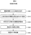
(無酸素銅スパッタリングターゲット材の製造方法)
図2は、本発明の実施の形態に係る無酸素銅スパッタリングターゲット材の製造工程の流れの一例を示す。
(Method for producing oxygen-free copper sputtering target material)
FIG. 2 shows an example of the flow of the manufacturing process of the oxygen-free copper sputtering target material according to the embodiment of the present invention.
まず、純度が99.9%以上の無酸素銅を鋳造して、所定の圧延処理を施すことにより、所定寸法の板材を製作する(S100)。この板材は、一例として、0.2mm以下の平均結晶粒径を有する。板材は、複数枚(少なくとも2枚)製作する。次に、2枚の板材の側面を互いに突き合わせて固定する(S110)。続いて、一方の板材の側面と他方の板材の側面とが突き合わされた部分である接合部分としての突き合わせ部を、FSW接合により接合する(S120)。これにより、接合部分が形成される。また、FSW接合による結晶組織への影響は摩擦撹拌部としての接合部分に略限定され、非接合部分としての接合部分を除く一方の板材及び他方の板材は、接合前の結晶組織が維持される。 First, an oxygen-free copper having a purity of 99.9% or more is cast and subjected to a predetermined rolling process to produce a plate material having a predetermined dimension (S100). As an example, this plate material has an average crystal grain size of 0.2 mm or less. A plurality of (at least two) plate materials are produced. Next, the side surfaces of the two plates are brought into contact with each other and fixed (S110). Subsequently, a butted portion as a joining portion, which is a portion where the side surface of one plate material and the side surface of the other plate material are abutted, is joined by FSW joining (S120). Thereby, a junction part is formed. In addition, the influence of the FSW bonding on the crystal structure is substantially limited to the bonded portion as the friction stirrer, and the crystal structure before bonding is maintained on one plate member and the other plate member excluding the bonded portion as the non-bonded portion. .
次に、接合した材料の表面及び裏面を所定の深さずつ研削する(S130)。続いて、所定の真空度を有する真空中において、接合部分を有する一方の板材及び他方の板材に対して、無酸素銅に対してアニール効果があり、かつ、無酸素銅の平均結晶粒径がそれほど粗大化しない温度で熱処理を施す(S140)。熱処理は、一例として、400℃から500℃の温度範囲で所定時間、真空中において実施する。これにより、接合部分が接合部10となり、非接合部分が非接合部12に変化して、本実施の形態に係る無酸素銅スパッタリングターゲット材1が製造される。なお、研削する工程は、熱処理の工程の後に実施することもできる。
Next, the front and back surfaces of the joined materials are ground by a predetermined depth (S130). Subsequently, in a vacuum having a predetermined degree of vacuum, there is an annealing effect on oxygen-free copper with respect to one plate material and the other plate material having a joint portion, and the average crystal grain size of oxygen-free copper is Heat treatment is performed at a temperature that is not so coarse (S140). For example, the heat treatment is performed in a vacuum at a temperature range of 400 ° C. to 500 ° C. for a predetermined time. Thereby, a junction part turns into the junction part 10, a non-joint part changes into the
図3は、本発明の実施の形態に係る無酸素銅スパッタリングターゲット材の製造工程におけるFSW接合の概要を示す斜視図であり、図4は、本発明の実施の形態に係る無酸素銅スパッタリングターゲット材の製造工程におけるFSW接合の概要を示す断面図である。 FIG. 3 is a perspective view showing an outline of FSW bonding in the manufacturing process of the oxygen-free copper sputtering target material according to the embodiment of the present invention, and FIG. 4 is an oxygen-free copper sputtering target according to the embodiment of the present invention. It is sectional drawing which shows the outline | summary of the FSW joining in the manufacturing process of material.
FSW接合は、先端に所定形状の突起34を有する回転ツール30を所定の方向に所定の回転速度で回転させ、回転している回転ツール30の突起34を、一方の板材としての板材20aと他方の板材としての板材22aとが接触している部分に押し込むことにより、突起34と各板材との間に生じた摩擦熱によって各板材の所定の領域を軟化させ、軟化した各板材の所定の領域を攪拌して接合する手法である。
In FSW bonding, a
すなわち、本実施の形態においては、図3に示すように、ショルダ32及び突起34を有する回転ツール30を所定の方向(例えば、図3における「A」の方向)に所定の回転速度で回転させつつ、被接合材料としての板材20a及び板材22aに所定の深さまで突起34を挿入する。そして、突き合わせ部24に沿って回転ツール30を板材20a及び板材22aに対して相対的に移動させ、突き合わせ部24に沿って板材20aの側面20bと板材22aの側面22bとを接合する。具体的には、回転ツール30を、板材20a及び板材22aの長手方向(例えば、図3における「B」の方向)に所定の速度で移動させる。
That is, in the present embodiment, as shown in FIG. 3, the
そして、図4に示すように、板材20a及び板材22aと突起34とが接して突起34が回転することにより摩擦熱が生じて、生じた摩擦熱により板材20a及び板材22aの一部がそれぞれ軟化して摩擦攪拌部40となり、流動化する。そして、摩擦攪拌部40が固化することにより、板材20aと板材22aとが接続部分10bを介して接合される。摩擦熱により流動化する部分は摩擦攪拌部40に略限定され、板材20aと板材22aとが固相で接合するので、接続部分10bの金属組織は微細化している。すなわち、接続部分10bの結晶粒組織は、板材20a及び板材22aの結晶粒組織に比べて、機械的特性に優れた微細な組織となる。
Then, as shown in FIG. 4, the
例えば、平均結晶粒径が0.2mm以下程度の無酸素銅からなる板材20aと板材22aとをFSW接合を用いて接合すると、平均結晶粒径が0.02mm以上0.03mm以下程度の板材20aの平均結晶粒径と板材22aの平均結晶粒径よりも小さい平均結晶粒径を有する細かい結晶粒を含む結晶粒組織の接続部分10bが得られる。FSW接合による結晶組織への影響は、上述したように摩擦攪拌部40に略限定される。
For example, when the
したがって、平均結晶粒径が0.2mm以下程度の板材20aと板材22aとを接合すると、接続部分10bの平均結晶粒径は0.02mm以上0.03mm以下程度となり、熱処理前の非接合部分(板材20a及び板材22aから接合部分10bを除いた部分)の平均結晶粒径は、板材20a及び板材22aの平均結晶粒径(0.2mm以下程度)を引き継ぐこととなる。続いて、板材20aと板材22aとが接合部分10bによって接合された材料に所定の熱処理を施すことにより、接続部分10bから形成された接合部10と非接続部分から形成された非接合部12とが形成される。そして、接合部10の結晶粒組織と非接合部12の結晶粒組織とが略同程度である本実施の形態に係る無酸素銅スパッタリングターゲット材1が得られる。
Therefore, when the
本実施の形態に係る無酸素銅スパッタリングターゲット材1は、一例として、薄膜トランジスタ(Thin Film Transistor:TFT)等の電子部品における電極配線の形成に用いることができる。例えば、無酸素銅スパッタリングターゲット材1は、ディスプレイパネルにおける電極配線の形成用途として用いることができる。 As an example, the oxygen-free copper sputtering target material 1 according to the present embodiment can be used for forming an electrode wiring in an electronic component such as a thin film transistor (TFT). For example, the oxygen-free copper sputtering target material 1 can be used for forming electrode wiring in a display panel.
(実施の形態の効果)
本実施の形態に係る無酸素銅スパッタリングターゲット材1は、アルミニウム系(抵抗率:4μΩcm程度)よりも低抵抗である無酸素銅(抵抗率:2μΩcm程度)からなる複数の板材を摩擦攪拌接合により接合して、接合後に熱処理を施すことにより、接合部10の平均結晶粒径と非接合部12の平均結晶粒径との差を低減することができる。すなわち、接合部10の平均結晶粒径と非接合部12の平均結晶粒径とを同程度にすることができる。したがって、例えば、液晶パネルの大型化に伴って大面積化したガラス基板よりも広い面積を有するスパッタリングターゲット材であって、スパッタリングによるターゲットエロージョンの接合部10と非接合部12との間における進行の差を低減させ、安定したスパッタリングができる無酸素銅スパッタリングターゲット材1を提供することができる。
(Effect of embodiment)
The oxygen-free copper sputtering target material 1 according to the present embodiment is formed by friction stir welding a plurality of plate materials made of oxygen-free copper (resistivity: about 2 μΩcm) having a lower resistance than that of an aluminum system (resistivity: about 4 μΩcm). By joining and heat-treating after joining, the difference between the average crystal grain size of the joint 10 and the average crystal grain size of the non-joint 12 can be reduced. That is, the average crystal grain size of the joint portion 10 and the average crystal grain size of the
すなわち、本実施の形態に係る無酸素銅スパッタリングターゲット材の製造方法によれば、一例として、第8世代の液晶パネル用ガラス基板のサイズ2200mm×2400mmよりも広い面積(例えば、約3m角で厚さが10mm以上)の無酸素銅スパッタリングターゲット材1であって、接合部分と非接合部分とでスパッタリングによるターゲットエロージョンの進行の差が実質的に生じずに、安定したスパッタリングができる大型基板用途としての無酸素銅スパッタリングターゲット材1を提供することができる。 That is, according to the method for manufacturing an oxygen-free copper sputtering target material according to the present embodiment, as an example, an area larger than the size 2200 mm × 2400 mm of the glass substrate for an 8th generation liquid crystal panel (for example, about 3 m square and thick). As an oxygen-free copper sputtering target material 1 having a thickness of 10 mm or more), a large-sized substrate application capable of stable sputtering without substantially causing a difference in the progress of target erosion due to sputtering between a bonded portion and a non-bonded portion. The oxygen-free copper sputtering target material 1 can be provided.
また、本実施の形態においてはスパッタリングターゲット材の原料として無酸素銅を用いており、無酸素銅は、アルミニウム、純銅、及びZr、Sn、又はAg等を添加した銅に比べて高い導電性(低い電気抵抗)を有する。したがって、本実施の形態に係る無酸素銅スパッタリングターゲット材1は、例えば、電極の配線材料として用いるのに有利である。 In this embodiment, oxygen-free copper is used as a raw material for the sputtering target material. The oxygen-free copper has higher conductivity than aluminum, pure copper, and copper added with Zr, Sn, Ag, or the like ( Low electrical resistance). Therefore, the oxygen-free copper sputtering target material 1 according to the present embodiment is advantageous for use as an electrode wiring material, for example.
本発明の実施例に係る無酸素銅スパッタリングターゲット材は、以下の工程を採用して製造した。まず、99.99%の純度の無酸素銅を鋳造した。そして、鋳造して得られた無酸素銅に熱間圧延処理と、中間熱処理と、冷間圧延処理とを施すことにより、厚さ15mm×幅500mm×長さ3000mmである4種類の板材を製作した。具体的に、中間熱処理における処理温度と、冷間圧延処理における加工パススケジュールとを適宜変更することにより、平均結晶粒径が0.02mmの板材A(実施例1に係る板材)と、平均結晶粒径が0.05mmの板材B(実施例2に係る板材)と、平均結晶粒径が0.1mmの板材C(実施例3に係る板材)と、平均結晶粒径が0.2mmの板材D(実施例4に係る板材)とを製作した。ここで、板材の平均結晶粒径は、JIS H 0510に基づいて、標準写真と板材の写真との比較法により測定した。 The oxygen-free copper sputtering target material according to the example of the present invention was manufactured by employing the following steps. First, oxygen-free copper having a purity of 99.99% was cast. And, four kinds of plate materials of 15mm thickness x width 500mm x length 3000mm are manufactured by performing hot rolling treatment, intermediate heat treatment, and cold rolling treatment on oxygen-free copper obtained by casting. did. Specifically, by appropriately changing the treatment temperature in the intermediate heat treatment and the processing pass schedule in the cold rolling treatment, a plate material A (plate material according to Example 1) having an average crystal grain size of 0.02 mm, and an average crystal Plate material B having a particle size of 0.05 mm (plate material according to Example 2), Plate material C having an average crystal grain size of 0.1 mm (plate material according to Example 3), and plate material having an average crystal grain size of 0.2 mm D (plate material according to Example 4) was manufactured. Here, the average crystal grain size of the plate material was measured by a comparison method between a standard photograph and a plate material photograph based on JIS H0510.
また、比較例として、中間熱処理の処理温度と、冷間圧延処理の加工パススケジュールとをそれぞれ適宜変更することにより、平均結晶粒径が0.3mmの板材E(比較例1に係る板材)と、平均結晶粒径が0.5mmの板材F(比較例2に係る板材)とをそれぞれ製作した。 In addition, as a comparative example, by appropriately changing the processing temperature of the intermediate heat treatment and the processing pass schedule of the cold rolling process, the plate material E (plate material according to comparative example 1) having an average crystal grain size of 0.3 mm and A plate material F (plate material according to Comparative Example 2) having an average crystal grain size of 0.5 mm was produced.
次に、同一粒径の板材同士、すなわち、一方の板材Aと他方の板材Aとを長手方向の側面で突き合わせて併置・固定した(これにより、厚さ15mm×幅1000mm×長さ3000mmとなる)。続いて、一方の板材Aと他方の板材Aとの突き合わせ部分をFSW接合により接合した。同様にして、板材Bから板材Dについて、FSW接合により接合した。これにより、実施例に係る板材のそれぞれから、接合材料を得た。 Next, the plate materials having the same particle diameter, that is, one plate material A and the other plate material A were abutted and fixed on the side surfaces in the longitudinal direction (thus, thickness 15 mm × width 1000 mm × length 3000 mm). ). Subsequently, the butted portion between one plate material A and the other plate material A was joined by FSW joining. Similarly, the plate material B to the plate material D were joined by FSW joining. Thereby, a bonding material was obtained from each of the plate materials according to the example.
ここで、一方の板材と他方の板材とが接合している接合部分に隣接する非接合部分は、接合部分から離れている非接合部分と同一の結晶粒組織を有していた。すなわち、板材Aから板材DのそれぞれからFSW接合により接合した接合材料のそれぞれにおいて、非接合部分の平均結晶粒径は、接合前の板材の平均結晶粒径とそれぞれ同一であった。また、板材Aから板材DのそれぞれからFSW接合により接合した接合材料のそれぞれにおいて、一方の板材と他方の板材との接合部分の平均結晶粒径は、板材Aから板材Dのそれぞれから作成した材料のいずれにおいても、0.02mmであった。 Here, the non-joining portion adjacent to the joint portion where one plate member and the other plate member are joined has the same crystal grain structure as the non-joint portion separated from the joint portion. That is, in each of the joining materials joined by FSW joining from each of the plate materials A to D, the average crystal grain size of the non-joined portion was the same as the average crystal grain size of the plate material before joining. Moreover, in each of the joining materials joined by FSW joining from each of the plate materials A to D, the average crystal grain size of the joining portion between one plate material and the other plate material is a material created from each of the plate materials A to D. In both cases, it was 0.02 mm.
また、実施例に係る板材Aから板材Dと同様にして、一方の板材Eと他方の板材EとをFSW接合により接合することにより、比較例1に係る接合材料を得た。同様にして、板材Fから比較例2に係る接合材料を得た。ここで、板材E及び板材FのそれぞれからFSW接合により接合した接合材料のそれぞれにおいて、一方の板材と他方の板材との接合部分の平均結晶粒径は、実施例に係る板材Aから板材Dと同様に、板材E及び板材Fのそれぞれから作成した材料のいずれにおいても、0.02mmから0.03mmであった。また、比較例1及び2における非接合部分の平均結晶粒径についても、実施例1から4と同様に、接合部分に隣接する非接合部分と、接合部分から離れている非接合部分とは同一の結晶粒組織を有しており、それぞれ接合前の板材の平均結晶粒径と同一の平均結晶粒径を有していた。 Moreover, it joined to the board | plate material A which concerns on the Example from the board | plate material D, and joined one board | plate material E and the other board | plate material E by FSW joining, and the joining material which concerns on the comparative example 1 was obtained. Similarly, the bonding material according to Comparative Example 2 was obtained from the plate material F. Here, in each of the joining materials joined by FSW joining from each of the plate material E and the plate material F, the average crystal grain size of the joint portion between one plate material and the other plate material is the plate material A to the plate material D according to the example. Similarly, it was 0.02 mm to 0.03 mm in any of the materials prepared from each of the plate material E and the plate material F. Moreover, also about the average crystal grain diameter of the non-joining part in Comparative Examples 1 and 2, as in Examples 1 to 4, the non-joining part adjacent to the joining part and the non-joining part separated from the joining part are the same. Each having an average crystal grain size identical to the average crystal grain size of the plate material before joining.
次に、実施例(実施例1から4)及び比較例(比較例1及び2)に係る接合材料の表面及び裏面を、それぞれの表面から2mmの深さまで研削した。続いて、真空中、400℃で、2時間の熱処理を、実施例(実施例1から4)及び比較例(比較例1及び2)に係る接合材料のそれぞれに施した。これにより、実施例(実施例1から4)及び比較例(比較例1及び2)に係る無酸素銅スパッタリングターゲット材を作成した。 Next, the front and back surfaces of the bonding materials according to Examples (Examples 1 to 4) and Comparative Examples (Comparative Examples 1 and 2) were ground to a depth of 2 mm from the respective surfaces. Subsequently, heat treatment was performed in vacuum at 400 ° C. for 2 hours to each of the bonding materials according to the examples (Examples 1 to 4) and the comparative examples (Comparative Examples 1 and 2). Thus, oxygen-free copper sputtering target materials according to Examples (Examples 1 to 4) and Comparative Examples (Comparative Examples 1 and 2) were prepared.
表1に、本発明の実施例及び比較例に係る板材、及び無酸素銅スパッタリングターゲット材の熱処理前後における接合部並びに非接合部の平均結晶粒径を示す。 Table 1 shows the average crystal grain sizes of the bonded portions and the non-bonded portions before and after the heat treatment of the plate materials and the oxygen-free copper sputtering target materials according to Examples and Comparative Examples of the present invention.

表1を参照すると分かるように、実施例(実施例1から4)に係る無酸素銅スパッタリングターゲット材(すなわち、熱処理後の接合材料)の接合部10の平均結晶粒径はそれぞれ、板材Aから板材Dのそれぞれの平均結晶粒径によらず0.04mmから0.06mmで略同一であった。また、実施例(実施例1から4)に係る無酸素銅スパッタリングターゲット材(すなわち、熱処理後の接合材料)の非接合部12の平均結晶粒径は、用いた板材の粒径により0.04mmから0.1mmの間で変動した。
As can be seen from Table 1, the average crystal grain size of the joint 10 of the oxygen-free copper sputtering target material (that is, the joint material after the heat treatment) according to the example (Examples 1 to 4) is from the plate material A, respectively. Regardless of the average grain size of each of the plate materials D, it was substantially the same from 0.04 mm to 0.06 mm. Further, the average crystal grain size of the
例えば、実施例1においては、平均結晶粒径が0.02mmの板材Aから形成した無酸素銅スパッタリングターゲット材の非接合部12の平均結晶粒径は0.04mmであった。また、実施例2においては、平均結晶粒径が0.05mmの板材Bから形成した無酸素銅スパッタリングターゲット材の非接合部12の平均結晶粒径は0.06mmであった。また、平均結晶粒径が0.1mmの板材Cから形成した無酸素銅スパッタリングターゲット材の非接合部12の平均結晶粒径は0.08mmであった。更に、平均結晶粒径が0.2mmの板材Dから形成した無酸素銅スパッタリングターゲット材の非接合部12の平均結晶粒径は0.1mmであった。
For example, in Example 1, the average crystal grain size of the
ここで、比較例(比較例1及び2)に係る無酸素銅スパッタリングターゲット材(すなわち、熱処理後の接合材料)の接合部10の平均結晶粒径はそれぞれ、実施例1から4の場合と同様に、0.05mmから0.06mmで略同一であった。一方、比較例1及び2における無酸素銅スパッタリングターゲット材(すなわち、熱処理後の接合材料)の非接合部12は、微細な再結晶粒と接合前の元の平均結晶粒径に近い粗大な結晶粒とが混合した混粒状態であることが観察された。
Here, the average crystal grain size of the joint portion 10 of the oxygen-free copper sputtering target material (that is, the joint material after the heat treatment) according to the comparative example (Comparative Examples 1 and 2) is the same as that in each of Examples 1 to 4. Furthermore, it was substantially the same from 0.05 mm to 0.06 mm. On the other hand, the
次に、実施例(実施例1から4)及び比較例(比較例1及び2)に係る無酸素銅スパッタリングターゲット材のそれぞれについて、接合部10を含むようにφ100mmの円形状に切り抜いた。このようにして、実施例(実施例1から4)に係る無酸素銅スパッタリングターゲット材のそれぞれから、実施例(実施例1から4)に係る実験用の無酸素銅スパッタリングターゲット2を作成すると共に、比較例(比較例1及び2)に係る無酸素銅スパッタリングターゲット材のそれぞれから、比較例(比較例1及び2)に係る実験用の無酸素銅スパッタリングターゲットを作成した。 Next, each of the oxygen-free copper sputtering target materials according to Examples (Examples 1 to 4) and Comparative Examples (Comparative Examples 1 and 2) was cut out into a circular shape of φ100 mm so as to include the joint portion 10. Thus, while producing the oxygen free copper sputtering target 2 for experiment which concerns on an Example (Examples 1 to 4) from each of the oxygen free copper sputtering target material which concerns on an Example (Examples 1 to 4). From each of the oxygen-free copper sputtering target materials according to Comparative Examples (Comparative Examples 1 and 2), experimental oxygen-free copper sputtering targets according to Comparative Examples (Comparative Examples 1 and 2) were prepared.
図5は、本発明の実施例に係る実験用の無酸素銅スパッタリングターゲットのスパッタリング後の上面図を示す。 FIG. 5 shows a top view after sputtering of an experimental oxygen-free copper sputtering target according to an embodiment of the present invention.
実施例(実施例1から4)及び比較例(比較例1及び2)に係る実験用の無酸素銅スパッタリングターゲットを用いて、スパッタリングを実施した。スパッタリング装置としては、マグネトロンスパッタリング装置を使用した。スパッタリング条件は、以下のとおりである。すなわち、導入ガスとして1Paの圧力のアルゴン(Ar)ガスを用いると共に、RFパワーを300Wに設定してスパッタ処理の累計時間を180分とした。 Sputtering was performed using the oxygen-free copper sputtering target for experiments according to Examples (Examples 1 to 4) and Comparative Examples (Comparative Examples 1 and 2). A magnetron sputtering apparatus was used as the sputtering apparatus. The sputtering conditions are as follows. That is, argon (Ar) gas having a pressure of 1 Pa was used as the introduced gas, the RF power was set to 300 W, and the cumulative time of the sputtering process was 180 minutes.
スパッタリングの結果、スパッタリング後の無酸素銅スパッタリングターゲットの表面には、図5に示すように、スパッタリングが集中する領域に、リング状に窪んだエロージョン(侵食)領域50が形成された。 As a result of sputtering, an erosion (erosion) region 50 recessed in a ring shape was formed on the surface of the oxygen-free copper sputtering target after sputtering as shown in FIG.
実施例1から4に係る実験用の無酸素銅スパッタリングターゲット2においては、接合部10aと非接合部12aとの境界でのエロージョンの変化は目視では認められなかった。更に、実施例1から4に係る実験用の無酸素銅スパッタリングターゲット2においては、接合部10aと非接合部12aとの境界でエロージョンの進行には実質的に差が認められなかった。
In the experimental oxygen-free copper sputtering target 2 according to Examples 1 to 4, no change in erosion at the boundary between the bonded
一方、比較例1及び2に係る実験用の無酸素銅スパッタリングターゲットにおいては、スパッタリング後の無酸素銅スパッタリングターゲットの表面には、接合部と非接合部との境界が目立ち、それぞれの部分でのエロージョンの進行にかなり差があることが認められた。 On the other hand, in the oxygen-free copper sputtering target for experiments according to Comparative Examples 1 and 2, the boundary between the bonded portion and the non-bonded portion is conspicuous on the surface of the oxygen-free copper sputtering target after sputtering. It was recognized that there was a considerable difference in the progress of erosion.
また、実施例(実施例1から4)及び比較例(比較例1及び2)に係る無酸素銅スパッタリングターゲットのそれぞれについて、接合部10aと非接合部12aとでスパッタリングの状況の違いを定量的に調べることを目的として、接合部10aのエロージョン領域と非接合部12aのエロージョン領域それぞれの表面粗さをそれぞれ測定した。表面粗さは、JIS B0601に基づいて、算術平均粗さ(Ra)を測定した。なお、算術平均粗さの単位はμmである。ここで、エロージョン領域50のリング幅は20mm程度観察され、幅の中央部付近の3mm長について表面粗さを測定した。具体的に、接合部10aのエロージョン領域50に対応する部分(表面粗さ測定部分54)と、非接合部12aのエロージョン領域50に対応する部分(表面粗さ測定部分52)とのそれぞれについて、表面粗さを測定した。
Further, for each of the oxygen-free copper sputtering targets according to the examples (Examples 1 to 4) and the comparative examples (Comparative Examples 1 and 2), the difference in the sputtering situation between the bonded
表2は、本発明の実施例及び比較例に係る表面粗さの測定結果を示す。 Table 2 shows the measurement results of the surface roughness according to Examples and Comparative Examples of the present invention.
表2を参照すると、比較例1に係る実験用の無酸素銅スパッタリングターゲット材においては、接合部10aと非接合部12aとの間における表面粗さの相違は−34%であり、比較例2に係る実験用の無酸素銅スパッタリングターゲット材においては、接合部10aと非接合部12aとの間における表面粗さの相違は−36%であった。一方、実施例1から4に係る実験用の無酸素銅スパッタリングターゲット材においては、接合部10aと非接合部12aとの間における表面粗さの相違は、±7%から8%以内の相違であることが観察された。
Referring to Table 2, in the experimental oxygen-free copper sputtering target material according to Comparative Example 1, the difference in surface roughness between the bonded
この結果から、実施例1から4に係る無酸素銅スパッタリングターゲット材においては、接合部10aと非接合部12aとの間でエロージョンの進行の程度に大きな差がなく、比較例1及び2に係る無酸素銅スパッタリングターゲットよりも、安定したスパッタリングを実施することができることが示された。すなわち、比較例1及び2に係る無酸素銅スパッタリングターゲットではスパッタリングが不安定であり、スパッタリングによって形成される銅膜の均一性に影響を与える一方で、実施例1から4に係る無酸素銅スパッタリングターゲット2によれば、安定したスパッタリングができることが示された。
From this result, in the oxygen-free copper sputtering target material according to Examples 1 to 4, there is no significant difference in the degree of progress of erosion between the bonded
以上、本発明の実施の形態及び実施例を説明したが、上記に記載した実施の形態及び実施例は特許請求の範囲に係る発明を限定するものではない。また、実施の形態及び実施例の中で説明した特徴の組合せの全てが発明の課題を解決するための手段に必須であるとは限らない点に留意すべきである。 While the embodiments and examples of the present invention have been described above, the embodiments and examples described above do not limit the invention according to the claims. It should be noted that not all combinations of features described in the embodiments and examples are necessarily essential to the means for solving the problems of the invention.
1 無酸素銅スパッタリングターゲット材
2 無酸素銅スパッタリングターゲット
10、10a 接合部
10b 接続部分
12、12a 非接合部
20 第1の板材
20a、22a 板材
20b、22b 側面
22 第2の板材
24 突き合わせ部
30 回転ツール
32 ショルダ
34 突起
40 摩擦攪拌部
50 エロージョン領域
52、54 表面粗さ測定部分
DESCRIPTION OF SYMBOLS 1 Oxygen-free copper sputtering target material 2 Oxygen-free
Claims (5)
前記第1の板材と前記第2の板材との間に、前記第1の板材及び前記第2の板材から形成され、平均結晶粒径が0.04mm以上0.06mm以下である接合部と
を備える無酸素銅スパッタリングターゲット材。 A first plate material and a second plate material which are formed from a copper material made of oxygen-free copper having a purity of 3N or more, and whose average crystal grain size is 0.04 mm or more and 0.1 mm or less;
Between the first plate member and the second plate member, a joining portion formed from the first plate member and the second plate member and having an average crystal grain size of 0.04 mm or more and 0.06 mm or less. Oxygen free copper sputtering target material.
前記複数枚の板材の一方の板材の側面と他方の板材の側面とを突き合わせる突き合わせ工程と、
前記一方の板材の側面と前記他方の板材の側面とが突き合わされて形成される突き合わせ部を摩擦攪拌接合により接合して接合部分を形成する接合工程と、
前記接合部分と、前記接合部分により互いに接合した前記一方の板材及び前記他方の板材とに真空中で熱処理を施して、前記接合部分の結晶を粗大化させると共に、前記一方の板材及び前記他方の板材から前記接合部分を除いた部分である非接合部分に再結晶粒を生成させる熱処理工程と
を備える無酸素銅スパッタリングターゲット材の製造方法。 A plate material preparation step of preparing a plurality of plate materials made of copper material composed of oxygen-free copper;
A butting step of abutting the side surface of one plate member and the side surface of the other plate member of the plurality of plate members;
A joining step of joining a butted portion formed by abutting a side surface of the one plate material and a side surface of the other plate material by friction stir welding to form a joined portion;
The joint portion and the one plate member and the other plate member joined to each other by the joint portion are subjected to a heat treatment in a vacuum to coarsen crystals of the joint portion, and the one plate member and the other plate member. A method for producing an oxygen-free copper sputtering target material, comprising: a heat treatment step of generating recrystallized grains in a non-joined portion that is a portion obtained by removing the joined portion from a plate material.
前記接合工程は、平均結晶粒径が0.02mm以上0.03mm以下の前記接合部分を形成する
請求項3に記載の無酸素銅スパッタリングターゲット材の製造方法。 The plate material preparation step prepares the plurality of plate materials having an average crystal grain size of 0.2 mm or less,
The said joining process is a manufacturing method of the oxygen-free copper sputtering target material of Claim 3 which forms the said junction part whose average crystal grain diameter is 0.02 mm or more and 0.03 mm or less.
請求項3又は4に記載の無酸素銅スパッタリングターゲット材の製造方法。 The heat treatment step forms a joined portion having an average crystal grain size of 0.04 mm or more and 0.06 mm or less from the joined portion and a non-joined portion having an average crystal grain size of 0.04 mm or more and 0.1 mm or less. The manufacturing method of the oxygen-free copper sputtering target material of Claim 3 or 4 which forms a junction part.
Priority Applications (1)
| Application Number | Priority Date | Filing Date | Title |
|---|---|---|---|
| JP2008199265A JP5233486B2 (en) | 2008-08-01 | 2008-08-01 | Oxygen-free copper sputtering target material and method for producing oxygen-free copper sputtering target material |
Applications Claiming Priority (1)
| Application Number | Priority Date | Filing Date | Title |
|---|---|---|---|
| JP2008199265A JP5233486B2 (en) | 2008-08-01 | 2008-08-01 | Oxygen-free copper sputtering target material and method for producing oxygen-free copper sputtering target material |
Publications (2)
| Publication Number | Publication Date |
|---|---|
| JP2010037579A true JP2010037579A (en) | 2010-02-18 |
| JP5233486B2 JP5233486B2 (en) | 2013-07-10 |
Family
ID=42010435
Family Applications (1)
| Application Number | Title | Priority Date | Filing Date |
|---|---|---|---|
| JP2008199265A Expired - Fee Related JP5233486B2 (en) | 2008-08-01 | 2008-08-01 | Oxygen-free copper sputtering target material and method for producing oxygen-free copper sputtering target material |
Country Status (1)
| Country | Link |
|---|---|
| JP (1) | JP5233486B2 (en) |
Cited By (3)
| Publication number | Priority date | Publication date | Assignee | Title |
|---|---|---|---|---|
| JP2012111994A (en) * | 2010-11-24 | 2012-06-14 | Furukawa Electric Co Ltd:The | Cylindrical target material, its manufacturing method and its sheet coating method |
| JP2015120975A (en) * | 2013-11-25 | 2015-07-02 | 株式会社フルヤ金属 | Production method of sputtering target, and sputtering target |
| CN115106638A (en) * | 2022-07-15 | 2022-09-27 | 中国科学院空天信息创新研究院 | Welding method of thin-wall oxygen-free copper ring |
Citations (11)
| Publication number | Priority date | Publication date | Assignee | Title |
|---|---|---|---|---|
| JPH11158614A (en) * | 1997-11-28 | 1999-06-15 | Hitachi Metals Ltd | Copper target for sputtering and its production |
| JP2000034562A (en) * | 1998-07-14 | 2000-02-02 | Japan Energy Corp | Sputtering target and part used in apparatus for forming thin film |
| JP2001240949A (en) * | 2000-02-29 | 2001-09-04 | Mitsubishi Materials Corp | Method of manufacturing for worked billet of high- purity copper having fine crystal grain |
| JP2002110649A (en) * | 2000-10-03 | 2002-04-12 | Matsushita Electric Ind Co Ltd | Plasma treatment apparatus |
| JP2002220659A (en) * | 2000-12-05 | 2002-08-09 | Praxair St Technol Inc | Working and bonding of copper sputter target |
| JP2004204253A (en) * | 2002-12-24 | 2004-07-22 | Hitachi Metals Ltd | Target |
| JP2004211202A (en) * | 2002-12-26 | 2004-07-29 | Samsung Electronics Co Ltd | Sputtering target, sputtering chamber including the same and sputtering method |
| JP2004307906A (en) * | 2003-04-03 | 2004-11-04 | Kobelco Kaken:Kk | Sputtering target, and method for manufacturing the same |
| JP2005533187A (en) * | 2002-07-16 | 2005-11-04 | ハネウェル・インターナショナル・インコーポレーテッド | Copper sputtering target and method of forming copper sputtering target |
| JP2007226058A (en) * | 2006-02-24 | 2007-09-06 | Tosoh Corp | Liquid crystal display panel, its manufacturing method, and cu alloy sputtering target |
| JP2007290017A (en) * | 2006-04-26 | 2007-11-08 | Dowa Holdings Co Ltd | Method for welding copper member and friction stir welding equipment |
-
2008
- 2008-08-01 JP JP2008199265A patent/JP5233486B2/en not_active Expired - Fee Related
Patent Citations (11)
| Publication number | Priority date | Publication date | Assignee | Title |
|---|---|---|---|---|
| JPH11158614A (en) * | 1997-11-28 | 1999-06-15 | Hitachi Metals Ltd | Copper target for sputtering and its production |
| JP2000034562A (en) * | 1998-07-14 | 2000-02-02 | Japan Energy Corp | Sputtering target and part used in apparatus for forming thin film |
| JP2001240949A (en) * | 2000-02-29 | 2001-09-04 | Mitsubishi Materials Corp | Method of manufacturing for worked billet of high- purity copper having fine crystal grain |
| JP2002110649A (en) * | 2000-10-03 | 2002-04-12 | Matsushita Electric Ind Co Ltd | Plasma treatment apparatus |
| JP2002220659A (en) * | 2000-12-05 | 2002-08-09 | Praxair St Technol Inc | Working and bonding of copper sputter target |
| JP2005533187A (en) * | 2002-07-16 | 2005-11-04 | ハネウェル・インターナショナル・インコーポレーテッド | Copper sputtering target and method of forming copper sputtering target |
| JP2004204253A (en) * | 2002-12-24 | 2004-07-22 | Hitachi Metals Ltd | Target |
| JP2004211202A (en) * | 2002-12-26 | 2004-07-29 | Samsung Electronics Co Ltd | Sputtering target, sputtering chamber including the same and sputtering method |
| JP2004307906A (en) * | 2003-04-03 | 2004-11-04 | Kobelco Kaken:Kk | Sputtering target, and method for manufacturing the same |
| JP2007226058A (en) * | 2006-02-24 | 2007-09-06 | Tosoh Corp | Liquid crystal display panel, its manufacturing method, and cu alloy sputtering target |
| JP2007290017A (en) * | 2006-04-26 | 2007-11-08 | Dowa Holdings Co Ltd | Method for welding copper member and friction stir welding equipment |
Cited By (3)
| Publication number | Priority date | Publication date | Assignee | Title |
|---|---|---|---|---|
| JP2012111994A (en) * | 2010-11-24 | 2012-06-14 | Furukawa Electric Co Ltd:The | Cylindrical target material, its manufacturing method and its sheet coating method |
| JP2015120975A (en) * | 2013-11-25 | 2015-07-02 | 株式会社フルヤ金属 | Production method of sputtering target, and sputtering target |
| CN115106638A (en) * | 2022-07-15 | 2022-09-27 | 中国科学院空天信息创新研究院 | Welding method of thin-wall oxygen-free copper ring |
Also Published As
| Publication number | Publication date |
|---|---|
| JP5233486B2 (en) | 2013-07-10 |
Similar Documents
| Publication | Publication Date | Title |
|---|---|---|
| JP4784602B2 (en) | Sputtering target, method for producing the same, and method for regenerating sputtering target using the method | |
| JP4422975B2 (en) | Sputtering target and manufacturing method thereof | |
| TW460600B (en) | Sputter target | |
| JP6491859B2 (en) | Sputtering target manufacturing method and sputtering target | |
| JP4237479B2 (en) | Sputtering target, Al alloy film and electronic parts | |
| JP5233486B2 (en) | Oxygen-free copper sputtering target material and method for producing oxygen-free copper sputtering target material | |
| JP2013019010A (en) | Copper material for sputtering target and method for production thereof | |
| JP2009057598A (en) | Sputtering target | |
| JP2003226966A (en) | Large target material | |
| JP2000345326A (en) | Divided ito sputtering target | |
| WO2012140928A1 (en) | Sputtering target for solar cell | |
| WO2005059198A1 (en) | Aluminum base target and process for producing the same | |
| JP2004204253A (en) | Target | |
| TW202003888A (en) | Sputtering target and manufacturing method thereof | |
| JP5233485B2 (en) | Oxygen-free copper sputtering target material and method for producing oxygen-free copper sputtering target material | |
| JP4162467B2 (en) | Manufacturing method of sputtering target | |
| JP2006316339A (en) | Aluminum-based sputtering target | |
| JPH1161395A (en) | Ito sputtering target | |
| JP2008156694A (en) | Sputtering target material and its production method | |
| WO2023145620A1 (en) | Heat treatment method for dissimilar metal joint material and resulting dissimilar metal joint material | |
| JP2006159223A (en) | METHOD FOR PRODUCING Al OR Al ALLOY JOINED BODY | |
| JP2001316806A (en) | High purity al target and wiring film | |
| JPH02243790A (en) | Titanium electrocoated face plate drum and its production | |
| JP2011058078A (en) | SPUTTERING TARGET, Ta-W ALLOY FILM USING THE SAME, AND LIQUID CRYSTAL DISPLAY DEVICE | |
| WO2013088785A1 (en) | Indium sputtering target member and method for producing same |
Legal Events
| Date | Code | Title | Description |
|---|---|---|---|
| A621 | Written request for application examination |
Free format text: JAPANESE INTERMEDIATE CODE: A621 Effective date: 20101119 |
|
| A977 | Report on retrieval |
Free format text: JAPANESE INTERMEDIATE CODE: A971007 Effective date: 20120328 |
|
| A131 | Notification of reasons for refusal |
Free format text: JAPANESE INTERMEDIATE CODE: A131 Effective date: 20120918 |
|
| A521 | Written amendment |
Free format text: JAPANESE INTERMEDIATE CODE: A523 Effective date: 20121116 |
|
| TRDD | Decision of grant or rejection written | ||
| A01 | Written decision to grant a patent or to grant a registration (utility model) |
Free format text: JAPANESE INTERMEDIATE CODE: A01 Effective date: 20130226 |
|
| A61 | First payment of annual fees (during grant procedure) |
Free format text: JAPANESE INTERMEDIATE CODE: A61 Effective date: 20130311 |
|
| R150 | Certificate of patent or registration of utility model |
Free format text: JAPANESE INTERMEDIATE CODE: R150 |
|
| FPAY | Renewal fee payment (event date is renewal date of database) |
Free format text: PAYMENT UNTIL: 20160405 Year of fee payment: 3 |
|
| LAPS | Cancellation because of no payment of annual fees |