JP2010028051A - Method of manufacturing multilayered printed wiring board - Google Patents
Method of manufacturing multilayered printed wiring board Download PDFInfo
- Publication number
- JP2010028051A JP2010028051A JP2008191223A JP2008191223A JP2010028051A JP 2010028051 A JP2010028051 A JP 2010028051A JP 2008191223 A JP2008191223 A JP 2008191223A JP 2008191223 A JP2008191223 A JP 2008191223A JP 2010028051 A JP2010028051 A JP 2010028051A
- Authority
- JP
- Japan
- Prior art keywords
- conductive
- substrate sheet
- sheet
- conductive bumps
- printed wiring
- Prior art date
- Legal status (The legal status is an assumption and is not a legal conclusion. Google has not performed a legal analysis and makes no representation as to the accuracy of the status listed.)
- Granted
Links
Images


Abstract
Description
本発明は、多層プリント配線板を製造するための多層プリント配線板製造方法に関する。 The present invention relates to a multilayer printed wiring board manufacturing method for manufacturing a multilayer printed wiring board.
従来より、銅箔等の基板シートの表面に複数の略円錐状の導電性バンプが形成された導電性バンプ付基板シートと、プリプレグ等の非導電性シート(絶縁シート)とを交互に重ね合わせることにより形成される多層プリント配線板が知られている。このような多層プリント配線板において、基板シートの表面に形成された導電性バンプが絶縁シートを貫通することによって、当該絶縁シートの両側にある基板シート同士が導電性バンプによって電気的に接続されるようになっている(例えば、特許文献1乃至3等参照)。
Conventionally, a substrate sheet with conductive bumps, in which a plurality of substantially conical conductive bumps are formed on the surface of a substrate sheet such as copper foil, and a non-conductive sheet (insulating sheet) such as a prepreg are alternately stacked. A multilayer printed wiring board formed by this method is known. In such a multilayer printed wiring board, when the conductive bump formed on the surface of the substrate sheet penetrates the insulating sheet, the substrate sheets on both sides of the insulating sheet are electrically connected by the conductive bump. (See, for example,
導電性バンプ付基板シートの形成方法について、図13および図14を用いて説明する。基板シートに複数の導電性バンプを形成するにあたり、例えばメタルマスク版等からなるスクリーン版92、およびスキージ96を用いるようなスクリーン印刷方法(孔版印刷方法)が用いられる。
A method for forming the substrate sheet with conductive bumps will be described with reference to FIGS. In forming a plurality of conductive bumps on the substrate sheet, a screen printing method (stencil printing method) using a
具体的には、まず、図13に示すような平板状の基板シート80を印刷定盤90上に載置し、この平板状の基板シート80の上方にわずかな距離を隔ててスクリーン版92を設置する。この際に、印刷定盤90上に載置された基板シート80に対してスクリーン版92の位置合わせをCCDカメラ(図示せず)等により行い、このスクリーン版92の両端部を保持部材94により保持する。また、図14に示すようにスクリーン版92には、基板シート80に導電性バンプ82が形成されるべき位置に対応して複数の貫通穴(版孔)92aが形成されている。そして、図13および図14に示すように、スキージ96により導電性ペースト98の塗工を行い、この際に図14に示すようにスキージ96がスクリーン版92を下方に押圧してこのスクリーン版92と基板シート80とを当接させることにより、導電性ペースト98はスクリーン版92の貫通穴92aを通過して平板状の基板シート80上に付着する。
Specifically, first, a
ここで、スキージ96によるスクリーン版92を介した導電性ペースト98の塗工原理についてより詳細に説明すると、導電性ペースト98はスキージ96によってスクリーン版92の表面に沿って移動させられるが、スクリーン版92に貫通穴92aが形成されている箇所においてはこの貫通穴92aに導電性ペースト98が入り込む。そして、図14に示すようにスキージ96がスクリーン版92を基板シート80に向かって押圧することによって、貫通穴92aに入った導電性ペースト98の一部が基板シート80上に付着することとなる。
Here, the principle of applying the
スキージ96を用いたスクリーン印刷方法により基板シート80上に導電性ペースト98を付着させた後、この基板シート80の乾燥を行う。このことにより、図15に示すように基板シート80上の導電性ペースト98が熱硬化して略円錐状の導電性バンプ82が形成されることとなる。
After the
ここで、基板シート80に形成される導電性バンプ82は、当該基板シート80の厚さ方向(図15の上下方向)において絶縁シート(図示せず)を貫通させるのに十分な高さが必要とされる。また、多層プリント配線板のファインピッチ化を行う場合には、略円錐状の導電性バンプ82について、同じ高さであっても底面積が小さくなるような形状、すなわちいわゆるアスペクト比の高い略円錐状とする必要がある。
Here, the
また、他のスクリーン印刷方法としては、例えば特許文献4等に示すようなものが知られている。特許文献4に開示されるスクリーン印刷方法においては、表面に凹凸のある印刷基板の凸部頂点にのみペースト類を転写するようになっている。具体的には、スクリーン版と印刷基板との間に、ゴムまたは軟質樹脂で形成された弾性ロールを介在させ、スクリーン版上のペースト類をいったん弾性ロールに転写し、弾性ロールを回転させながら当該弾性ロールに転写されたペースト類を印刷基板の凸部頂点に転写するようになっている。 Further, as another screen printing method, for example, the one shown in Patent Document 4 is known. In the screen printing method disclosed in Patent Document 4, pastes are transferred only to the vertices of convex portions of a printed board having a concavo-convex surface. Specifically, an elastic roll formed of rubber or a soft resin is interposed between the screen plate and the printing substrate, the paste on the screen plate is once transferred to the elastic roll, and the elastic roll is rotated while the elastic roll is rotated. The paste transferred to the elastic roll is transferred to the apex of the convex portion of the printing substrate.
しかしながら、従来の導電性バンプ付基板シートの製造方法においては、平板状の基板シート80上に導電性バンプ82を形成するにあたり、スクリーン印刷工程1回あたりの基板シート80に付着する導電性ペースト98の量はスクリーン版92の貫通穴92aにより定められるため、この導電性ペースト98の量が十分ではなく1回のスクリーン印刷工程では導電性バンプ82の高さが絶縁シートを貫通させるのに十分な高さに達しない場合が多い。図面を用いてより詳細に説明すると、図15(a)〜(d)は、従来の方法により基板シート80に導電性バンプ82が形成される過程を示す図であって、(a)は1回目のスクリーン印刷工程および乾燥工程後の導電性バンプ82の形状を示し、(b)は2回目のスクリーン印刷工程および乾燥工程後の導電性バンプ82の形状を示している。また、図15(c)は3回目のスクリーン印刷工程および乾燥工程後の導電性バンプ82の形状を示し、(d)は4回目のスクリーン印刷工程および乾燥工程後の導電性バンプ82の形状を示している。
However, in the conventional method of manufacturing a substrate sheet with conductive bumps, when forming the
ここで、導電性バンプ82により絶縁シートを貫通させる際に、図15(d)に示すような高さを有する略円錐状の導電性バンプ82が求められる。このため、図13に示すようなスクリーン印刷工程を複数回、具体的には例えば4回繰り返して行うことが必要とされる。しかしながら、スクリーン印刷工程を1回行うたびに基板シート80の乾燥工程およびCCDカメラ等によるスクリーン版92の位置合わせ工程が必要となり、十分な高さの導電性バンプ82が形成されるまでこれらの工程を何度も繰り返す必要があった。また、上述のようなスクリーン印刷工程の回数を減らした場合には、基板シート80に形成された導電性バンプ82の先端形状が細くなり、基板シート80と絶縁シートとを交互に重ね合わせたときに、絶縁シートを突き破った導電性バンプ82の先端部分とこの絶縁シートに当接する他の基板シートとが接触する面積が小さくなり、この導電性バンプ82を介して接続される絶縁シートを挟んだ2つの基板シート間における抵抗値が大きくなるという問題があった。
Here, when the insulating sheet is penetrated by the
本発明は、このような点を考慮してなされたものであり、非導電性シートを突き破った導電性バンプの先端部分とこの非導電性シートに当接する他の導電性バンプ付基板シートとが接触する面積が大きくなり、このため導電性バンプを介して接続される非導電性シートを挟んだ導電性バンプ付基板シート間の抵抗値が小さくなるような多層プリント配線板を製造することができる多層プリント配線板製造方法を提供することを目的とする。 The present invention has been made in consideration of such points, and the tip portion of the conductive bump that broke through the non-conductive sheet and the other conductive bump-attached substrate sheet that contacts the non-conductive sheet are provided. A multilayer printed wiring board can be manufactured in which the contact area is large, and therefore the resistance value between the conductive bump-attached substrate sheets sandwiching the nonconductive sheet connected via the conductive bumps is small. It aims at providing the manufacturing method of a multilayer printed wiring board.
本発明は、複数の導電性バンプが表面に形成された導電性バンプ付基板シートと、非導電性シートとが交互に重ね合わせられており、前記導電性バンプが前記非導電性シートを貫通することにより当該非導電性シートの両側にある導電性バンプ付基板シート同士が前記導電性バンプによって電気的に接続されているような多層プリント配線板を製造するための多層プリント配線板製造方法であって、平板状の基板シートを準備する工程と、前記各導電性バンプが形成されるべき各々の箇所において前記平板状の基板シートを変形させることにより、この基板シートにおいて前記各導電性バンプが形成されるべき各々の箇所にそれぞれ凹部を形成する工程と、複数の凹部が形成された前記基板シートの表面において当該各凹部に導電性バンプを形成させて導電性バンプ付基板シートを製造する工程と、前記導電性バンプ付基板シートと、前記非導電性シートとを重ね合わせ、この重ね合わせ体を挟圧し、この際に前記導電性バンプ付基板シートにおける前記基板シートに形成された前記各凹部をそれぞれ凸部に変形させ、このようにして前記導電性バンプ付基板シートの前記導電性バンプが前記非導電性シートを突き破るようにする工程と、前記導電性バンプが前記非導電性シートを突き破ったような前記重ね合わせ体を積層することにより多層プリント配線板を製造する工程と、を備えたことを特徴とする多層プリント配線板製造方法である。 In the present invention, the substrate sheet with conductive bumps on the surface of which a plurality of conductive bumps are formed and the nonconductive sheet are alternately superposed, and the conductive bumps penetrate the nonconductive sheet. A multilayer printed wiring board manufacturing method for manufacturing a multilayer printed wiring board in which the conductive bump-equipped board sheets on both sides of the nonconductive sheet are electrically connected by the conductive bumps. The step of preparing a flat substrate sheet and the step of forming the conductive bumps on the substrate sheet by deforming the flat plate substrate sheet at each location where the conductive bumps are to be formed. A step of forming a recess at each location to be formed, and a conductive bump on each recess on the surface of the substrate sheet on which a plurality of recesses are formed. The step of manufacturing the substrate sheet with conductive bumps, the substrate sheet with conductive bumps, and the non-conductive sheet are overlapped, and the overlapped body is sandwiched, and at this time, the conductive bumps attached A step of deforming each concave portion formed on the substrate sheet in the substrate sheet into a convex portion, and thus allowing the conductive bumps of the substrate sheet with conductive bumps to break through the non-conductive sheet; And a step of producing a multilayer printed wiring board by laminating the superposed body in which the conductive bumps break through the non-conductive sheet. is there.
このような多層プリント配線板製造方法によれば、基板シートにおいて各導電性バンプが形成されるべき各々の箇所にそれぞれ凹部を予め形成しておき、この基板シートの各凹部の中に導電性バンプを形成し、その後、導電性バンプ付基板シートと、非導電性シートとを重ね合わせ、この重ね合わせ体を挟圧するときに、導電性バンプが形成された基板シートの各凹部をそれぞれ凸部に変形させるようにしている。そして、導電性バンプ付基板シートと非導電性シートとの重ね合わせ体を挟圧することにより導電性バンプ付基板シートの導電性バンプが非導電性シートを突き破るようにし、導電性バンプが非導電性シートを突き破ったような重ね合わせ体を積層することにより多層プリント配線板を製造している。ここで、導電性バンプが形成された基板シートの各凹部をそれぞれ凸部に変形させたときに、凹部の中に形成された導電性バンプが基板シートの表面からより一層突き出るようになる。このため、非導電性シートを突き破った導電性バンプの先端部分とこの非導電性シートに当接する他の導電性バンプ付基板シートとが接触する面積が大きくなる。このことにより、導電性バンプを介して接続される非導電性シートを挟んだ導電性バンプ付基板シート間における抵抗値が小さくなるような多層プリント配線板を製造することができるようになる。 According to such a multilayer printed wiring board manufacturing method, a concave portion is formed in advance in each portion where each conductive bump is to be formed in the substrate sheet, and the conductive bump is formed in each concave portion of the substrate sheet. After that, the substrate sheet with conductive bumps and the non-conductive sheet are overlapped, and when the stacked body is sandwiched, each concave portion of the substrate sheet on which the conductive bumps are formed is formed as a convex portion. I am trying to deform. Then, the conductive bump of the substrate sheet with conductive bumps breaks through the non-conductive sheet by sandwiching the laminated body of the substrate sheet with conductive bumps and the non-conductive sheet, and the conductive bumps are non-conductive. A multilayer printed wiring board is manufactured by laminating superposed bodies that break through sheets. Here, when each concave portion of the substrate sheet on which the conductive bump is formed is deformed into a convex portion, the conductive bump formed in the concave portion further protrudes from the surface of the substrate sheet. For this reason, the area which the front-end | tip part of the conductive bump which broke through the nonelectroconductive sheet and the board | substrate sheet | seat with another electroconductive bump contact | abutted to this nonelectroconductive sheet contacts becomes large. This makes it possible to manufacture a multilayer printed wiring board in which the resistance value between the substrate sheets with conductive bumps sandwiching the nonconductive sheet connected via the conductive bumps becomes small.
本発明の多層プリント配線板製造方法においては、複数の突起が表面に形成された平板状部材を準備する工程を更に備え、前記導電性バンプ付基板シートと前記非導電性シートとの重ね合わせ体を挟圧する際に、前記平板状部材における前記各突起が設けられた面に前記導電性バンプ付基板シートを載せ、この際に前記平板状部材における前記各突起が設けられた面と前記導電性バンプ付基板シートにおける前記導電性バンプが形成されていない面とが当接するようにし、これらの平板状部材、導電性バンプ付基板シートおよび非導電性シートを一体的に挟圧することにより、前記平板状部材に設けられた前記各突起により前記導電性バンプ付基板シートにおける前記基板シートに形成された前記各凹部をそれぞれ凸部に変形させることが好ましい。この際に、前記平板状部材には、当該平板状部材に載せられるべき前記導電性バンプ付基板シートにおける前記基板シートに形成された前記各凹部と位置が合うよう、各突起が設けられていることがより一層好ましい。 In the multilayer printed wiring board manufacturing method of the present invention, the method further comprises a step of preparing a flat plate member having a plurality of protrusions formed on the surface thereof, and a laminate of the substrate sheet with conductive bumps and the non-conductive sheet When the substrate is clamped, the substrate sheet with conductive bumps is placed on the surface of the flat plate member on which the protrusions are provided. At this time, the surface of the flat plate member on which the protrusions are provided and the conductive material The flat plate is formed by bringing the flat plate member, the conductive bump-equipped substrate sheet, and the non-conductive sheet together into pressure contact so that the surface on which the conductive bump is not formed in the substrate sheet with bump is brought into contact. Preferably, each of the concave portions formed on the substrate sheet of the conductive bump-equipped substrate sheet is deformed into a convex portion by the projections provided on the shaped member. Arbitrariness. At this time, the flat plate member is provided with projections so as to be aligned with the concave portions formed in the substrate sheet of the conductive bump-equipped substrate sheet to be placed on the flat plate member. It is even more preferable.
本発明の多層プリント配線板製造方法によれば、非導電性シートを突き破った導電性バンプの先端部分とこの非導電性シートに当接する他の導電性バンプ付基板シートとが接触する面積が大きくなり、このため導電性バンプを介して接続される非導電性シートを挟んだ導電性バンプ付基板シート間における抵抗値が小さくなるような多層プリント配線板が得られる。 According to the multilayer printed wiring board manufacturing method of the present invention, the contact area between the leading end portion of the conductive bump that has broken through the non-conductive sheet and the other conductive bump-attached substrate sheet that contacts the non-conductive sheet is large. Therefore, a multilayer printed wiring board is obtained in which the resistance value between the conductive bump-equipped board sheets sandwiching the non-conductive sheet connected via the conductive bumps becomes small.
以下、図面を参照して本発明の実施の形態について説明する。図1乃至図12は、本発明による多層プリント配線板の製造方法の一の実施の形態を示す図である。 Embodiments of the present invention will be described below with reference to the drawings. 1 to 12 are diagrams showing an embodiment of a method for producing a multilayer printed wiring board according to the present invention.
このうち、図1は、導電性バンプ付基板シートの製造方法において、平板状の基板シート、および複数の突起が表面に形成された平板状部材を準備したときの状態を示す側面図であり、図2は、図1に示す平板状の基板シートおよび平板状部材を当接させてこの組合せ体を挟圧する方法を示す側面図であり、図3は、図2に示す方法により製造された、複数の凹部が表面に形成された基板シートを示す側面図である。また、図4は、図1に示す平板状の基板シートおよび平板状部材を当接させてこの組合せ体を挟圧する他の方法を示す側面図である。 Among these, FIG. 1 is a side view showing a state when preparing a flat plate-like substrate sheet and a flat plate-like member having a plurality of protrusions formed on the surface in the method of manufacturing a substrate sheet with conductive bumps, FIG. 2 is a side view showing a method of pressing the combined body by bringing the flat substrate sheet and the flat member shown in FIG. 1 into contact with each other, and FIG. 3 is manufactured by the method shown in FIG. It is a side view which shows the board | substrate sheet | seat in which the several recessed part was formed in the surface. FIG. 4 is a side view showing another method of pressing the combined body by bringing the flat substrate sheet and the flat member shown in FIG. 1 into contact with each other.
また、図5乃至図8は、図3に示す基板シートに導電性バンプを形成する動作の一連の流れを順に示す側面図であり、図9は、図7の部分拡大側面図である。また、図10は、図5乃至図8に示す方法により製造された導電性バンプ付基板シートを示す側面図である。
また、図11は、多層プリント配線板の製造方法において、複数の突起が表面に形成された平板状部材の上に図10に示す導電性バンプ付基板シートおよび非導電性シートを載せ、これらの平板状部材、導電性バンプ付基板シートおよび非導電性シートを挟圧することにより導電性バンプ付基板シートの導電性バンプが非導電性シートを突き破るようにする処理を示す側面図であり、図12は、図11に示す処理により形成される、導電性バンプが非導電性シートを突き破ったような重ね合わせ体を積層することにより製造される多層プリント配線板を示す側面図である。
5 to 8 are side views sequentially showing a series of operations for forming conductive bumps on the substrate sheet shown in FIG. 3, and FIG. 9 is a partially enlarged side view of FIG. FIG. 10 is a side view showing a substrate sheet with conductive bumps manufactured by the method shown in FIGS.
Further, FIG. 11 shows a method for manufacturing a multilayer printed wiring board, in which a substrate sheet with conductive bumps and a non-conductive sheet shown in FIG. 10 are placed on a flat plate member having a plurality of protrusions formed on the surface thereof. FIG. 12 is a side view showing a process in which the conductive bumps of the substrate sheet with conductive bumps break through the non-conductive sheet by sandwiching the flat plate member, the substrate sheet with conductive bumps and the non-conductive sheet; These are side views which show the multilayer printed wiring board manufactured by laminating | stacking the laminated body which the conductive bump formed through the process shown in FIG. 11 and pierced the nonelectroconductive sheet.
以下、導電性バンプ付基板シートの製造方法および多層プリント配線板の製造方法について順次説明する。 Hereinafter, a method for manufacturing a substrate sheet with conductive bumps and a method for manufacturing a multilayer printed wiring board will be sequentially described.
〔導電性バンプ付基板シートの製造方法〕
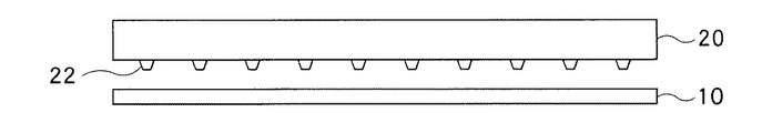
まず、図1に示すように、平板状の銅箔等の導電性の金属シートからなる基板シート10、および複数の突起22が形成された平板状部材20を準備する。ここで、平板状部材20は、銅、ステンレス、アルミニウム等の金属シートや、PET、PP、PE等のフィルム、あるいは樹脂シート等から構成されている。また、各突起22は、金属や樹脂等から構成されており、平板状部材20に対して後述するスクリーン印刷や、光造型法、エッチング、電鋳加工等を行うことにより形成されるようになっている。平板状部材20における各突起22が形成される位置は、基板シート10に導電性バンプ14(後述)が形成されるべき位置と略同一となるようにする。なお、平板状部材20に対して後述するスクリーン印刷方法(図5乃至図9に示すスクリーン印刷方法と類似の印刷方法)により各突起22を形成した場合は、導電性バンプ14(後述)が形成されるべき位置に対するこの突起22の見当合わせを容易に行うことができるようになる。
[Method of manufacturing substrate sheet with conductive bumps]
First, as shown in FIG. 1, a
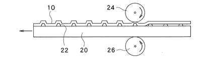
次に、平板状の基板シート10の表面(図1における基板シート10の上側の面)と平板状部材20における複数の突起22が形成された表面(図1における平板状部材20の下側の面)とを当接させる。そして、図2に示すように、この基板シート10および平板状部材20の組合せ体を、一対のゴムロール(挟圧ロール)24、26の間で挟圧する。具体的には、各々が連続的に回転する一対のゴムロール24、26の間に基板シート10および平板状部材20の組合せ体を搬送し、図2の矢印に示す方向に当該組合せ体を移動させることにより、基板シート10および平板状部材20の組合せ体は上下方向から挟圧されることとなる。このことにより、基板シート10の表面(図2における基板シート10の下側の面)が平板状部材20の各突起22に押圧され、基板シート10が変形し、図3に示すように基板シート10の表面に複数の凹部12が形成されるようになる。ここで、平板状部材20における各突起22が形成される位置は、基板シート10に導電性バンプ14が形成されるべき位置と略同一になっているので、基板シート10に形成される各凹部12の位置も、当該基板シート10に導電性バンプ14が形成されるべき位置と略同一になる。
Next, the surface of the flat substrate sheet 10 (the upper surface of the
なお、基板シート10を変形させて複数の凹部12を形成する方法は、図2に示すような方法に限定されることはなく、他の様々な方法を用いることができる。例えば、図4に示すように、基板シート10および平板状部材20の組合せ体を印刷定盤28に乗せ、加圧ロール29によりこの印刷定盤28上に載置された基板シート10が下方に押圧されるように印刷定盤28を図4の左右方向に移動させることによって、基板シート10における平板状部材20の各突起22が当接する箇所に複数の凹部12が形成されるようになる。このように、平板状の基板シート10の表面と平板状部材20における各突起22が形成された表面とを当接させてこの組合せ体を挟圧することにより、平板状の基板シート10に凹部12を形成することができるようになる。
Note that the method of forming the plurality of
次に、図5乃至図8に示すように、複数の凹部12が形成された基板シート10に対してスクリーン印刷を行う。
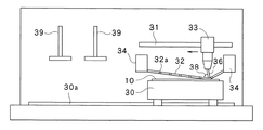
このようなスクリーン印刷を行う印刷装置は、基板シート10を吸引孔(図示せず)からの吸引力によって保持する印刷定盤30と、所定のパターンからなる複数の貫通穴(版孔)32aが設けられたメタルマスク等のスクリーン版32と、このスクリーン版32を保持する保持部材34とを備えている。ここで、各貫通穴32aは、基板シート10に導電性バンプ14が形成されるべき位置に対応するようスクリーン版32に形成されている。また、印刷装置は、スクリーン版32上で走査し、スクリーン版32に載置された銀ペースト、半田ペーストなどの導電性ペースト38を貫通穴32aを介して基板シート10上に転移させるスキージ36と、スキージ36を支持する支持部材33と、支持部材33を水平方向(図5の左右方向)に移動させるよう案内を行うガイド部材31とを備えている。支持部材33は、スキージ36を図5の下方に進出させたり上方に退避させたりすることができるようになっている。さらに、印刷装置は、印刷定盤30上にある基板シート10の表面の撮像を行うCCDカメラ39を備えている。また、印刷定盤30の下方にはガイド部材30aが配置されている。印刷定盤30は、ガイド部材30aに沿って水平方向(図5の左右方向)に移動可能となっている。
Next, as shown in FIGS. 5 to 8, screen printing is performed on the
A printing apparatus that performs such screen printing includes a
次に、上述のような印刷装置によるスクリーン印刷方法について説明する。まず、図5に示すように、印刷定盤30の上に基板シート10を載置し、吸引孔(図示せず)からの吸引力によって印刷定盤30上に基板シート10を保持させる。このときに、基板シート10に位置合わせマークを予め設けておくことにより、この位置合わせマークをCCDカメラ39で撮像し、撮像された画像における位置合わせマークに基づいて印刷定盤30の位置を微調整することにより、基板シート10に形成された各凹部12の位置と、スクリーン版32の貫通穴32aの位置とを容易に位置合わせすることができるようになる。
Next, a screen printing method using the above printing apparatus will be described. First, as shown in FIG. 5, the
そして、図6に示すように、印刷定盤30をガイド部材30aに沿って水平方向(図5の右方)に移動させ、この印刷定盤30をスクリーン版32の下方に位置させる。この際に、スクリーン版32の各貫通穴32aが基板シート10の各凹部12に向き合うようになる。
Then, as shown in FIG. 6, the
そして、図7に示すように、スキージ36が支持部材33から下方に進出し、このスキージ36がスクリーン版32を下方に押してスクリーン版32が印刷定盤30上の基板シート10の表面に当接する。そして、図7および図9に示すように、支持部材33をガイド部材31に沿って水平方向(図7の左方向)に移動させることによりスキージ36を水平方向(図7の左方向)に移動させ、このときにスキージ36がスクリーン版32を下方に押し続けるようにする。この際に、導電性ペースト38はスクリーン版32の貫通穴32aを通過して基板シート10の凹部12の中に付着する。
Then, as shown in FIG. 7, the
ここで、スキージ36によるスクリーン版32を介した導電性ペースト38の塗工原理についてより詳細に説明すると、導電性ペースト38はスキージ36によってスクリーン版32の表面を移動させられるが、スクリーン版32に貫通穴32aが形成されている箇所においてはこの貫通穴32aに導電性ペースト38が入り込む。そして、図9等に示すようにスクリーン版32の貫通穴32aは基板シート10の凹部12に対応して設けられているので、スキージ36がスクリーン版32を基板シート10に向かって押圧することによって、貫通穴32aに入った導電性ペースト38の一部が基板シート10の凹部12の中に付着することとなる。
Here, the principle of application of the
そして、図8に示すようにスキージ36による導電性ペースト38の塗工が終了したら、スキージ36が図8の上方に退避し、スクリーン版32が基板シート10から隔離される。
When the application of the
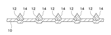
スキージ36を用いたスクリーン印刷方法により基板シート10の各凹部12の中に導電性ペースト38を付着させた後、この基板シート10の乾燥を行う。このことにより、図10に示すように基板シート10の各凹部12の中に付着した導電性ペースト38が熱硬化して略円錐状の導電性バンプ14が形成されることとなる。
After the
〔多層プリント配線板の製造方法〕
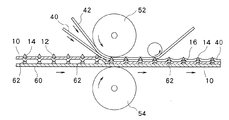
次に、図11および図12を用いて多層プリント配線板の製造方法について説明する。図11は、複数の突起62が表面に形成された平板状部材60の上に図10に示す導電性バンプ14付きの基板シート10およびプリプレグ等の非導電性シート(絶縁シート)40を載せ、これらの平板状部材60、導電性バンプ14付きの基板シート10および非導電性シート40を挟圧することにより導電性バンプ14が非導電性シート40を突き破るようにする処理を示す側面図であり、図12は、図11に示す処理により形成される、導電性バンプ14が非導電性シート40を突き破ったような重ね合わせ体を積層することにより製造される多層プリント配線板50を示す側面図である。
[Manufacturing method of multilayer printed wiring board]
Next, the manufacturing method of a multilayer printed wiring board is demonstrated using FIG. 11 and FIG. 11, the
多層プリント配線板の製造方法において、まず、複数の突起62が表面に形成された平板状部材60を準備する。ここで、図11に示すように、平板状部材60には、当該平板状部材60に載せられるべき導電性バンプ14付きの基板シート10における各凹部12と位置が合うよう、各突起62が設けられている。
In the method of manufacturing a multilayer printed wiring board, first, a
更に具体的には、平板状部材60は、銅、ステンレス、アルミニウム等の金属シートや、PET、PP、PE等のフィルム、あるいは樹脂シート等から構成されている。また、各突起62は、金属や樹脂等から構成されており、平板状部材60に対して図5乃至図9に示すようなスクリーン印刷や、光造型法、エッチング、電鋳加工等を行うことにより形成されるようになっている。前述のように、平板状部材60における各突起62が形成される位置は、基板シート10に凹部12が形成された位置と略同一となるようにしているが、平板状部材60に対して図5乃至図9に示すようなスクリーン印刷方法により各突起62を形成した場合は、基板シート10における凹部12が形成された位置に対するこの突起62の見当合わせを容易に行うことができるようになる。
More specifically, the
そして、図11に示すように、複数の突起62が表面に形成された平板状部材60と、導電性バンプ14付きの基板シート10と、非導電性シート40と、緩衝材42とを重ね合わせ、この重ね合わせ体を一対のゴムローラ(挟圧ローラ)52、54の間で非常に大きな力で挟圧する。ここで、各部材を重ね合わせる際に、平板状部材60における各突起62が設けられた面と基板シート10における導電性バンプ14が設けられていない面とが当接するようにし、しかも、平板状部材における各突起62と基板シート10における各凹部12との位置合わせを行うようにする。
Then, as shown in FIG. 11, the
また、上述の重ね合わせ体を挟圧するときに、図示しないヒータにより例えば100℃〜150℃で加熱も行うようにする。 Further, when sandwiching the above-described superposed body, heating is performed at, for example, 100 ° C. to 150 ° C. by a heater (not shown).
図11に示すように、上述の重ね合わせ体を挟圧したときに、平板状部材60に設けられた各突起62により、基板シート10に形成された各凹部12がそれぞれ凸部16に変形する。具体的には、平板状部材60には、当該平板状部材60に載せられるべき導電性バンプ14付きの基板シート10における各凹部12と位置が合うよう、各突起62が設けられているので、重ね合わせ体が挟圧されたときに、基板シート10はその裏面(図11における下側の面)から各突起62により上方に押圧され、基板シート10における各突起62に押圧された部分が図11の上方に向かって凸形状となり、このようにして基板シート10に形成された各凹部12がそれぞれ凸部16に変形する。
As shown in FIG. 11, when the above-described stacked body is clamped, the
上述の重ね合わせ体が上下方向から挟圧されるとともに加熱され、しかも基板シート10に形成された各凹部12がそれぞれ凸部16に変形することにより、非導電性シート40の裏面(図11の下側の面)がその下方に設けられた基板シート10の導電性バンプ14の先端部分に押圧され、この非導電性シート40における押圧された箇所が破断される。このことにより導電性バンプ14が非導電性シート40を貫通する。
The above-described superposed body is sandwiched and heated from above and below, and each
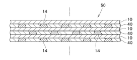
その後、上述の重ね合わせ体から平板状部材60および緩衝材42を取り除く。そして、導電性バンプ14が非導電性シート40を突き破ったような重ね合わせ体を何層にも重ねることにより、図12に示すような多層プリント配線板50が製造される。ここで、このように製造される多層プリント配線板50において、導電性バンプ14が非導電性シート40を貫通することにより、当該非導電性シート40の両側にある基板シート10同士が導電性バンプ14によって電気的に接続されることとなる。
Thereafter, the
以上のように本実施の形態の多層プリント配線板50の製造方法によれば、基板シート10において各導電性バンプ14が形成されるべき各々の箇所にそれぞれ凹部12を予め形成しておき、この基板シート10の各凹部12の中に導電性バンプ14を形成し、その後、導電性バンプ14付きの基板シート10と、非導電性シート40とを重ね合わせ、この重ね合わせ体を挟圧するときに、導電性バンプ14が形成された基板シート10の各凹部12をそれぞれ凸部16に変形させるようにしている。そして、導電性バンプ14付きの基板シート10と非導電性シート40との重ね合わせ体を挟圧することにより基板シート10の導電性バンプ14が非導電性シート40を突き破るようにし、導電性バンプ14が非導電性シート40を突き破ったような重ね合わせ体を積層することにより多層プリント配線板50を製造している。ここで、導電性バンプ14が形成された基板シート10の各凹部12をそれぞれ凸部16に変形させたときに、凹部12の中に形成された導電性バンプ14が基板シート10の表面からより一層突き出るようになる。このため、非導電性シート40を突き破った導電性バンプ14の先端部分とこの非導電性シート40に当接する他の基板シート10とが接触する面積が大きくなる。このことにより、導電性バンプ14を介して接続される非導電性シート40を挟んだ基板シート10間における抵抗値が小さくなるような多層プリント配線板50が得られる。このため、多層プリント配線板50の製造において、高抵抗値を有するような不良品の発生を抑制し、歩留まり率を向上させることができる。
As described above, according to the method for manufacturing the multilayer printed
10 基板シート
12 凹部
14 導電性バンプ
16 凸部
20 平板状部材
22 突起
24、26 一対のゴムロール
28 印刷定盤
29 加圧ロール
30 印刷定盤
30a ガイド部材
31 ガイド部材
32 スクリーン版
32a 貫通穴
33 支持部材
34 保持部材
36 スキージ
38 導電性ペースト
39 CCDカメラ
40 非導電性シート
42 緩衝材
50 多層プリント配線板
52、54 一対のゴムローラ
60 平板状部材
62 突起
80 基板シート
82 導電性バンプ
90 印刷定盤
92 スクリーン版
92a 貫通穴
94 保持部材
96 スキージ
98 導電性ペースト
DESCRIPTION OF
Claims (3)
平板状の基板シートを準備する工程と、
前記各導電性バンプが形成されるべき各々の箇所において前記平板状の基板シートを変形させることにより、この基板シートにおいて前記各導電性バンプが形成されるべき各々の箇所にそれぞれ凹部を形成する工程と、
複数の凹部が形成された前記基板シートの表面において当該各凹部に導電性バンプを形成させて導電性バンプ付基板シートを製造する工程と、
前記導電性バンプ付基板シートと、前記非導電性シートとを重ね合わせ、この重ね合わせ体を挟圧し、この際に前記導電性バンプ付基板シートにおける前記基板シートに形成された前記各凹部をそれぞれ凸部に変形させ、このようにして前記導電性バンプ付基板シートの前記導電性バンプが前記非導電性シートを突き破るようにする工程と、
前記導電性バンプが前記非導電性シートを突き破ったような前記重ね合わせ体を積層することにより多層プリント配線板を製造する工程と、
を備えたことを特徴とする多層プリント配線板製造方法。 A substrate sheet with conductive bumps having a plurality of conductive bumps formed on the surface and a non-conductive sheet are alternately superposed, and the non-conductive sheet penetrates the non-conductive sheet. A multilayer printed wiring board manufacturing method for manufacturing a multilayer printed wiring board in which the conductive bumped substrate sheets on both sides of the conductive sheet are electrically connected by the conductive bumps,
A step of preparing a flat substrate sheet;
The step of forming a concave portion at each location where each conductive bump is to be formed on the substrate sheet by deforming the flat substrate sheet at each location where each conductive bump is to be formed. When,
Producing a conductive bump-equipped substrate sheet by forming conductive bumps in the concave portions on the surface of the substrate sheet on which a plurality of concave portions are formed;
The substrate sheet with conductive bumps and the non-conductive sheet are overlapped, and the overlapped body is sandwiched between the respective concave portions formed on the substrate sheet in the substrate sheet with conductive bumps. Deforming into a convex portion, and thus making the conductive bumps of the substrate sheet with conductive bumps break through the non-conductive sheet;
A step of producing a multilayer printed wiring board by laminating the superposed body such that the conductive bumps break through the non-conductive sheet;
A multilayer printed wiring board manufacturing method characterized by comprising:
前記導電性バンプ付基板シートと前記非導電性シートとの重ね合わせ体を挟圧する際に、前記平板状部材における前記各突起が設けられた面に前記導電性バンプ付基板シートを載せ、この際に前記平板状部材における前記各突起が設けられた面と前記導電性バンプ付基板シートにおける前記導電性バンプが形成されていない面とが当接するようにし、これらの平板状部材、導電性バンプ付基板シートおよび非導電性シートを一体的に挟圧することにより、前記平板状部材に設けられた前記各突起により前記導電性バンプ付基板シートにおける前記基板シートに形成された前記各凹部をそれぞれ凸部に変形させることを特徴とする請求項1記載の多層プリント配線板製造方法。 Further comprising a step of preparing a plate-like member having a plurality of protrusions formed on the surface,
When sandwiching the overlapped body of the substrate sheet with conductive bumps and the non-conductive sheet, the substrate sheet with conductive bumps is placed on the surface of the flat plate member on which the projections are provided. So that the surface of the flat plate member on which the projections are provided and the surface of the substrate sheet with conductive bumps on which the conductive bumps are not formed are in contact with each other. By projecting the substrate sheet and the non-conductive sheet together, the respective protrusions formed on the substrate sheet in the substrate sheet with the conductive bumps are projected by the projections provided on the flat plate member. The multilayer printed wiring board manufacturing method according to claim 1, wherein the multilayer printed wiring board is deformed.
Priority Applications (1)
| Application Number | Priority Date | Filing Date | Title |
|---|---|---|---|
| JP2008191223A JP5120713B2 (en) | 2008-07-24 | 2008-07-24 | Multilayer printed wiring board manufacturing method |
Applications Claiming Priority (1)
| Application Number | Priority Date | Filing Date | Title |
|---|---|---|---|
| JP2008191223A JP5120713B2 (en) | 2008-07-24 | 2008-07-24 | Multilayer printed wiring board manufacturing method |
Publications (2)
| Publication Number | Publication Date |
|---|---|
| JP2010028051A true JP2010028051A (en) | 2010-02-04 |
| JP5120713B2 JP5120713B2 (en) | 2013-01-16 |
Family
ID=41733558
Family Applications (1)
| Application Number | Title | Priority Date | Filing Date |
|---|---|---|---|
| JP2008191223A Expired - Fee Related JP5120713B2 (en) | 2008-07-24 | 2008-07-24 | Multilayer printed wiring board manufacturing method |
Country Status (1)
| Country | Link |
|---|---|
| JP (1) | JP5120713B2 (en) |
Citations (3)
| Publication number | Priority date | Publication date | Assignee | Title |
|---|---|---|---|---|
| JPH1079579A (en) * | 1996-09-05 | 1998-03-24 | Toshiba Corp | Printed circuit board and manufacturing method of printed circuit board |
| JP2001326459A (en) * | 2000-05-16 | 2001-11-22 | North:Kk | Wiring circuit board and its manufacturing method |
| JP2006086153A (en) * | 2004-09-14 | 2006-03-30 | Sony Chem Corp | Flexible wiring board and its manufacturing method |
-
2008
- 2008-07-24 JP JP2008191223A patent/JP5120713B2/en not_active Expired - Fee Related
Patent Citations (3)
| Publication number | Priority date | Publication date | Assignee | Title |
|---|---|---|---|---|
| JPH1079579A (en) * | 1996-09-05 | 1998-03-24 | Toshiba Corp | Printed circuit board and manufacturing method of printed circuit board |
| JP2001326459A (en) * | 2000-05-16 | 2001-11-22 | North:Kk | Wiring circuit board and its manufacturing method |
| JP2006086153A (en) * | 2004-09-14 | 2006-03-30 | Sony Chem Corp | Flexible wiring board and its manufacturing method |
Also Published As
| Publication number | Publication date |
|---|---|
| JP5120713B2 (en) | 2013-01-16 |
Similar Documents
| Publication | Publication Date | Title |
|---|---|---|
| US9232662B2 (en) | Manufacturing method for wiring board | |
| JP5152663B2 (en) | Multilayer conductive bumped substrate sheet laminate manufacturing method and conductive bumped substrate sheet manufacturing method | |
| JP5120713B2 (en) | Multilayer printed wiring board manufacturing method | |
| JP5152658B2 (en) | Multilayer conductive bumped substrate sheet laminate manufacturing method, conductive bumped substrate sheet manufacturing method, conductive bumped substrate sheet, and substrate sheet | |
| JP5152659B2 (en) | Multilayer conductive bumped substrate sheet laminate manufacturing method and conductive bumped substrate sheet manufacturing method | |
| JP5067666B2 (en) | Printing device | |
| JP5067667B2 (en) | Printing method | |
| JP5088630B2 (en) | Method for manufacturing substrate sheet with conductive bump | |
| JP5035668B2 (en) | Method for producing substrate sheet with conductive bump and method for producing multilayer printed wiring board | |
| JP5034625B2 (en) | Multilayer printed wiring board manufacturing method | |
| JP5120717B2 (en) | Multilayer printed wiring board manufacturing method | |
| JP6078910B2 (en) | Printed wiring board manufacturing method, board combination, and printed wiring board | |
| JP2013021111A (en) | Manufacturing apparatus and manufacturing method of substrate sheet with conductive bump | |
| JP2010238756A (en) | Manufacturing method of substrate sheet with conductive bump and manufacturing method of multilayered printed wiring board | |
| JP5176819B2 (en) | Manufacturing method of multilayer printed wiring board | |
| JP2008262986A (en) | Manufacturing method of multilayer printed wiring board, and multilayer printed wiring board | |
| JP2006156908A (en) | Method for manufacturing printed circuit board | |
| JP2010251681A (en) | Manufacturing method of substrate sheet with conductive bump, manufacturing method of multilayer printed wiring board, and substrate sheet with conductive bump | |
| JP5332476B2 (en) | Substrate sheet manufacturing method with conductive bump and multilayer printed wiring board manufacturing method | |
| JP5262509B2 (en) | Printing device | |
| JP5056697B2 (en) | Printing device | |
| JP5067671B2 (en) | Method for manufacturing substrate sheet with conductive bump | |
| JP5109900B2 (en) | Method for manufacturing substrate sheet with conductive bump | |
| JP2009277799A (en) | Method of manufacturing multilayer electronic component | |
| JP2008124113A (en) | Method and device for manufacturing multilayer printed-wiring board |
Legal Events
| Date | Code | Title | Description |
|---|---|---|---|
| A621 | Written request for application examination |
Free format text: JAPANESE INTERMEDIATE CODE: A621 Effective date: 20110520 |
|
| A977 | Report on retrieval |
Free format text: JAPANESE INTERMEDIATE CODE: A971007 Effective date: 20120920 |
|
| TRDD | Decision of grant or rejection written | ||
| A01 | Written decision to grant a patent or to grant a registration (utility model) |
Free format text: JAPANESE INTERMEDIATE CODE: A01 Effective date: 20120928 |
|
| A01 | Written decision to grant a patent or to grant a registration (utility model) |
Free format text: JAPANESE INTERMEDIATE CODE: A01 |
|
| A61 | First payment of annual fees (during grant procedure) |
Free format text: JAPANESE INTERMEDIATE CODE: A61 Effective date: 20121011 |
|
| FPAY | Renewal fee payment (event date is renewal date of database) |
Free format text: PAYMENT UNTIL: 20151102 Year of fee payment: 3 |
|
| R150 | Certificate of patent or registration of utility model |
Free format text: JAPANESE INTERMEDIATE CODE: R150 |
|
| LAPS | Cancellation because of no payment of annual fees |