JP2010021013A - Photoelectric transfer element module - Google Patents
Photoelectric transfer element module Download PDFInfo
- Publication number
- JP2010021013A JP2010021013A JP2008180366A JP2008180366A JP2010021013A JP 2010021013 A JP2010021013 A JP 2010021013A JP 2008180366 A JP2008180366 A JP 2008180366A JP 2008180366 A JP2008180366 A JP 2008180366A JP 2010021013 A JP2010021013 A JP 2010021013A
- Authority
- JP
- Japan
- Prior art keywords
- photoelectric conversion
- conversion element
- counter electrode
- cable
- element module
- Prior art date
- Legal status (The legal status is an assumption and is not a legal conclusion. Google has not performed a legal analysis and makes no representation as to the accuracy of the status listed.)
- Granted
Links
- 239000000758 substrate Substances 0.000 claims abstract description 38
- 238000006243 chemical reaction Methods 0.000 claims description 193
- 239000003566 sealing material Substances 0.000 claims description 28
- 238000009434 installation Methods 0.000 abstract description 24
- 239000010410 layer Substances 0.000 description 73
- 239000004065 semiconductor Substances 0.000 description 20
- 239000000463 material Substances 0.000 description 16
- 239000003792 electrolyte Substances 0.000 description 13
- 239000000975 dye Substances 0.000 description 10
- 239000004020 conductor Substances 0.000 description 9
- 239000008151 electrolyte solution Substances 0.000 description 8
- 230000002165 photosensitisation Effects 0.000 description 8
- 239000003504 photosensitizing agent Substances 0.000 description 8
- BASFCYQUMIYNBI-UHFFFAOYSA-N platinum Chemical compound [Pt] BASFCYQUMIYNBI-UHFFFAOYSA-N 0.000 description 8
- 229910000679 solder Inorganic materials 0.000 description 8
- RTAQQCXQSZGOHL-UHFFFAOYSA-N Titanium Chemical compound [Ti] RTAQQCXQSZGOHL-UHFFFAOYSA-N 0.000 description 5
- 238000000034 method Methods 0.000 description 5
- 239000002245 particle Substances 0.000 description 5
- 229910052719 titanium Inorganic materials 0.000 description 5
- 239000010936 titanium Substances 0.000 description 5
- PXHVJJICTQNCMI-UHFFFAOYSA-N Nickel Chemical compound [Ni] PXHVJJICTQNCMI-UHFFFAOYSA-N 0.000 description 4
- 229910052697 platinum Inorganic materials 0.000 description 4
- XOLBLPGZBRYERU-UHFFFAOYSA-N tin dioxide Chemical compound O=[Sn]=O XOLBLPGZBRYERU-UHFFFAOYSA-N 0.000 description 4
- 229910001887 tin oxide Inorganic materials 0.000 description 4
- WEVYAHXRMPXWCK-UHFFFAOYSA-N Acetonitrile Chemical compound CC#N WEVYAHXRMPXWCK-UHFFFAOYSA-N 0.000 description 3
- XUIMIQQOPSSXEZ-UHFFFAOYSA-N Silicon Chemical compound [Si] XUIMIQQOPSSXEZ-UHFFFAOYSA-N 0.000 description 3
- 239000010408 film Substances 0.000 description 3
- 239000011245 gel electrolyte Substances 0.000 description 3
- 239000011521 glass Substances 0.000 description 3
- PCHJSUWPFVWCPO-UHFFFAOYSA-N gold Chemical compound [Au] PCHJSUWPFVWCPO-UHFFFAOYSA-N 0.000 description 3
- 229910052737 gold Inorganic materials 0.000 description 3
- 239000010931 gold Substances 0.000 description 3
- 150000002500 ions Chemical class 0.000 description 3
- 230000008018 melting Effects 0.000 description 3
- 238000002844 melting Methods 0.000 description 3
- 239000002114 nanocomposite Substances 0.000 description 3
- 239000005020 polyethylene terephthalate Substances 0.000 description 3
- 229920000139 polyethylene terephthalate Polymers 0.000 description 3
- 229920005989 resin Polymers 0.000 description 3
- 239000011347 resin Substances 0.000 description 3
- 229910052710 silicon Inorganic materials 0.000 description 3
- 239000010703 silicon Substances 0.000 description 3
- 239000012780 transparent material Substances 0.000 description 3
- -1 triiodide ions Chemical class 0.000 description 3
- YEJRWHAVMIAJKC-UHFFFAOYSA-N 4-Butyrolactone Chemical compound O=C1CCCO1 YEJRWHAVMIAJKC-UHFFFAOYSA-N 0.000 description 2
- RYGMFSIKBFXOCR-UHFFFAOYSA-N Copper Chemical compound [Cu] RYGMFSIKBFXOCR-UHFFFAOYSA-N 0.000 description 2
- BQCADISMDOOEFD-UHFFFAOYSA-N Silver Chemical compound [Ag] BQCADISMDOOEFD-UHFFFAOYSA-N 0.000 description 2
- QVGXLLKOCUKJST-UHFFFAOYSA-N atomic oxygen Chemical compound [O] QVGXLLKOCUKJST-UHFFFAOYSA-N 0.000 description 2
- 230000004888 barrier function Effects 0.000 description 2
- 229920001940 conductive polymer Polymers 0.000 description 2
- 229910052802 copper Inorganic materials 0.000 description 2
- 239000010949 copper Substances 0.000 description 2
- 239000013078 crystal Substances 0.000 description 2
- 239000007789 gas Substances 0.000 description 2
- 229910003437 indium oxide Inorganic materials 0.000 description 2
- PJXISJQVUVHSOJ-UHFFFAOYSA-N indium(iii) oxide Chemical compound [O-2].[O-2].[O-2].[In+3].[In+3] PJXISJQVUVHSOJ-UHFFFAOYSA-N 0.000 description 2
- 239000002608 ionic liquid Substances 0.000 description 2
- 239000007769 metal material Substances 0.000 description 2
- 229910044991 metal oxide Inorganic materials 0.000 description 2
- 150000004706 metal oxides Chemical class 0.000 description 2
- 229910052759 nickel Inorganic materials 0.000 description 2
- 239000003960 organic solvent Substances 0.000 description 2
- 229910052760 oxygen Inorganic materials 0.000 description 2
- 239000001301 oxygen Substances 0.000 description 2
- 239000004033 plastic Substances 0.000 description 2
- 229920003023 plastic Polymers 0.000 description 2
- 239000004417 polycarbonate Substances 0.000 description 2
- 229920000515 polycarbonate Polymers 0.000 description 2
- 229910052709 silver Inorganic materials 0.000 description 2
- 239000004332 silver Substances 0.000 description 2
- 238000005118 spray pyrolysis Methods 0.000 description 2
- 239000000126 substance Substances 0.000 description 2
- XLYOFNOQVPJJNP-UHFFFAOYSA-N water Chemical compound O XLYOFNOQVPJJNP-UHFFFAOYSA-N 0.000 description 2
- IKQCDTXBZKMPBB-UHFFFAOYSA-M 1-ethyl-3-methylimidazol-3-ium;iodide Chemical compound [I-].CCN1C=C[N+](C)=C1 IKQCDTXBZKMPBB-UHFFFAOYSA-M 0.000 description 1
- JFJNVIPVOCESGZ-UHFFFAOYSA-N 2,3-dipyridin-2-ylpyridine Chemical group N1=CC=CC=C1C1=CC=CN=C1C1=CC=CC=N1 JFJNVIPVOCESGZ-UHFFFAOYSA-N 0.000 description 1
- QKPVEISEHYYHRH-UHFFFAOYSA-N 2-methoxyacetonitrile Chemical compound COCC#N QKPVEISEHYYHRH-UHFFFAOYSA-N 0.000 description 1
- SFPQDYSOPQHZAQ-UHFFFAOYSA-N 2-methoxypropanenitrile Chemical compound COC(C)C#N SFPQDYSOPQHZAQ-UHFFFAOYSA-N 0.000 description 1
- YSHMQTRICHYLGF-UHFFFAOYSA-N 4-tert-butylpyridine Chemical compound CC(C)(C)C1=CC=NC=C1 YSHMQTRICHYLGF-UHFFFAOYSA-N 0.000 description 1
- 239000004925 Acrylic resin Substances 0.000 description 1
- 229920000178 Acrylic resin Polymers 0.000 description 1
- 229910017944 Ag—Cu Inorganic materials 0.000 description 1
- 229910018072 Al 2 O 3 Inorganic materials 0.000 description 1
- 229910015902 Bi 2 O 3 Inorganic materials 0.000 description 1
- ROFVEXUMMXZLPA-UHFFFAOYSA-N Bipyridyl Chemical group N1=CC=CC=C1C1=CC=CC=N1 ROFVEXUMMXZLPA-UHFFFAOYSA-N 0.000 description 1
- CPELXLSAUQHCOX-UHFFFAOYSA-M Bromide Chemical compound [Br-] CPELXLSAUQHCOX-UHFFFAOYSA-M 0.000 description 1
- WKBOTKDWSSQWDR-UHFFFAOYSA-N Bromine atom Chemical compound [Br] WKBOTKDWSSQWDR-UHFFFAOYSA-N 0.000 description 1
- OKTJSMMVPCPJKN-UHFFFAOYSA-N Carbon Chemical compound [C] OKTJSMMVPCPJKN-UHFFFAOYSA-N 0.000 description 1
- OIFBSDVPJOWBCH-UHFFFAOYSA-N Diethyl carbonate Chemical compound CCOC(=O)OCC OIFBSDVPJOWBCH-UHFFFAOYSA-N 0.000 description 1
- KMTRUDSVKNLOMY-UHFFFAOYSA-N Ethylene carbonate Chemical compound O=C1OCCO1 KMTRUDSVKNLOMY-UHFFFAOYSA-N 0.000 description 1
- 240000006829 Ficus sundaica Species 0.000 description 1
- YCKRFDGAMUMZLT-UHFFFAOYSA-N Fluorine atom Chemical compound [F] YCKRFDGAMUMZLT-UHFFFAOYSA-N 0.000 description 1
- 206010034972 Photosensitivity reaction Diseases 0.000 description 1
- 229920012266 Poly(ether sulfone) PES Polymers 0.000 description 1
- 239000012327 Ruthenium complex Substances 0.000 description 1
- 229910004298 SiO 2 Inorganic materials 0.000 description 1
- 229910020816 Sn Pb Inorganic materials 0.000 description 1
- 229910020836 Sn-Ag Inorganic materials 0.000 description 1
- 229910020888 Sn-Cu Inorganic materials 0.000 description 1
- 229910020922 Sn-Pb Inorganic materials 0.000 description 1
- 229910006404 SnO 2 Inorganic materials 0.000 description 1
- 229910020988 Sn—Ag Inorganic materials 0.000 description 1
- 229910019204 Sn—Cu Inorganic materials 0.000 description 1
- 229910008783 Sn—Pb Inorganic materials 0.000 description 1
- 229910010413 TiO 2 Inorganic materials 0.000 description 1
- GWEVSGVZZGPLCZ-UHFFFAOYSA-N Titan oxide Chemical compound O=[Ti]=O GWEVSGVZZGPLCZ-UHFFFAOYSA-N 0.000 description 1
- XLOMVQKBTHCTTD-UHFFFAOYSA-N Zinc monoxide Chemical compound [Zn]=O XLOMVQKBTHCTTD-UHFFFAOYSA-N 0.000 description 1
- NPNMHHNXCILFEF-UHFFFAOYSA-N [F].[Sn]=O Chemical compound [F].[Sn]=O NPNMHHNXCILFEF-UHFFFAOYSA-N 0.000 description 1
- 229910052782 aluminium Inorganic materials 0.000 description 1
- XAGFODPZIPBFFR-UHFFFAOYSA-N aluminium Chemical compound [Al] XAGFODPZIPBFFR-UHFFFAOYSA-N 0.000 description 1
- PNEYBMLMFCGWSK-UHFFFAOYSA-N aluminium oxide Inorganic materials [O-2].[O-2].[O-2].[Al+3].[Al+3] PNEYBMLMFCGWSK-UHFFFAOYSA-N 0.000 description 1
- 238000005452 bending Methods 0.000 description 1
- LRESCJAINPKJTO-UHFFFAOYSA-N bis(trifluoromethylsulfonyl)azanide;1-ethyl-3-methylimidazol-3-ium Chemical compound CCN1C=C[N+](C)=C1.FC(F)(F)S(=O)(=O)[N-]S(=O)(=O)C(F)(F)F LRESCJAINPKJTO-UHFFFAOYSA-N 0.000 description 1
- 229910000416 bismuth oxide Inorganic materials 0.000 description 1
- 229940006460 bromide ion Drugs 0.000 description 1
- GDTBXPJZTBHREO-UHFFFAOYSA-N bromine Substances BrBr GDTBXPJZTBHREO-UHFFFAOYSA-N 0.000 description 1
- 229910052794 bromium Inorganic materials 0.000 description 1
- 239000002041 carbon nanotube Substances 0.000 description 1
- 229910021393 carbon nanotube Inorganic materials 0.000 description 1
- 239000003575 carbonaceous material Substances 0.000 description 1
- 229910000420 cerium oxide Inorganic materials 0.000 description 1
- 239000011248 coating agent Substances 0.000 description 1
- 238000000576 coating method Methods 0.000 description 1
- 239000011258 core-shell material Substances 0.000 description 1
- 238000011161 development Methods 0.000 description 1
- 230000018109 developmental process Effects 0.000 description 1
- TYIXMATWDRGMPF-UHFFFAOYSA-N dibismuth;oxygen(2-) Chemical compound [O-2].[O-2].[O-2].[Bi+3].[Bi+3] TYIXMATWDRGMPF-UHFFFAOYSA-N 0.000 description 1
- 230000000694 effects Effects 0.000 description 1
- YQGOJNYOYNNSMM-UHFFFAOYSA-N eosin Chemical compound [Na+].OC(=O)C1=CC=CC=C1C1=C2C=C(Br)C(=O)C(Br)=C2OC2=C(Br)C(O)=C(Br)C=C21 YQGOJNYOYNNSMM-UHFFFAOYSA-N 0.000 description 1
- 239000003822 epoxy resin Substances 0.000 description 1
- 230000005496 eutectics Effects 0.000 description 1
- 229910052731 fluorine Inorganic materials 0.000 description 1
- 239000011737 fluorine Substances 0.000 description 1
- 239000011888 foil Substances 0.000 description 1
- 238000010438 heat treatment Methods 0.000 description 1
- 239000012943 hotmelt Substances 0.000 description 1
- AMGQUBHHOARCQH-UHFFFAOYSA-N indium;oxotin Chemical compound [In].[Sn]=O AMGQUBHHOARCQH-UHFFFAOYSA-N 0.000 description 1
- 238000002347 injection Methods 0.000 description 1
- 239000007924 injection Substances 0.000 description 1
- 238000004898 kneading Methods 0.000 description 1
- 239000002648 laminated material Substances 0.000 description 1
- MRELNEQAGSRDBK-UHFFFAOYSA-N lanthanum(3+);oxygen(2-) Chemical compound [O-2].[O-2].[O-2].[La+3].[La+3] MRELNEQAGSRDBK-UHFFFAOYSA-N 0.000 description 1
- 239000003446 ligand Substances 0.000 description 1
- DZVCFNFOPIZQKX-LTHRDKTGSA-M merocyanine Chemical compound [Na+].O=C1N(CCCC)C(=O)N(CCCC)C(=O)C1=C\C=C\C=C/1N(CCCS([O-])(=O)=O)C2=CC=CC=C2O\1 DZVCFNFOPIZQKX-LTHRDKTGSA-M 0.000 description 1
- 229910052751 metal Inorganic materials 0.000 description 1
- 239000002184 metal Substances 0.000 description 1
- 239000002105 nanoparticle Substances 0.000 description 1
- URLJKFSTXLNXLG-UHFFFAOYSA-N niobium(5+);oxygen(2-) Chemical compound [O-2].[O-2].[O-2].[O-2].[O-2].[Nb+5].[Nb+5] URLJKFSTXLNXLG-UHFFFAOYSA-N 0.000 description 1
- NJPPVKZQTLUDBO-UHFFFAOYSA-N novaluron Chemical compound C1=C(Cl)C(OC(F)(F)C(OC(F)(F)F)F)=CC=C1NC(=O)NC(=O)C1=C(F)C=CC=C1F NJPPVKZQTLUDBO-UHFFFAOYSA-N 0.000 description 1
- 230000033116 oxidation-reduction process Effects 0.000 description 1
- MPQXHAGKBWFSNV-UHFFFAOYSA-N oxidophosphanium Chemical compound [PH3]=O MPQXHAGKBWFSNV-UHFFFAOYSA-N 0.000 description 1
- BMMGVYCKOGBVEV-UHFFFAOYSA-N oxo(oxoceriooxy)cerium Chemical compound [Ce]=O.O=[Ce]=O BMMGVYCKOGBVEV-UHFFFAOYSA-N 0.000 description 1
- SIWVEOZUMHYXCS-UHFFFAOYSA-N oxo(oxoyttriooxy)yttrium Chemical compound O=[Y]O[Y]=O SIWVEOZUMHYXCS-UHFFFAOYSA-N 0.000 description 1
- WKMKTIVRRLOHAJ-UHFFFAOYSA-N oxygen(2-);thallium(1+) Chemical compound [O-2].[Tl+].[Tl+] WKMKTIVRRLOHAJ-UHFFFAOYSA-N 0.000 description 1
- SOQBVABWOPYFQZ-UHFFFAOYSA-N oxygen(2-);titanium(4+) Chemical compound [O-2].[O-2].[Ti+4] SOQBVABWOPYFQZ-UHFFFAOYSA-N 0.000 description 1
- RVTZCBVAJQQJTK-UHFFFAOYSA-N oxygen(2-);zirconium(4+) Chemical compound [O-2].[O-2].[Zr+4] RVTZCBVAJQQJTK-UHFFFAOYSA-N 0.000 description 1
- 229920000647 polyepoxide Polymers 0.000 description 1
- 239000011112 polyethylene naphthalate Substances 0.000 description 1
- 229920005672 polyolefin resin Polymers 0.000 description 1
- 238000007639 printing Methods 0.000 description 1
- RUOJZAUFBMNUDX-UHFFFAOYSA-N propylene carbonate Chemical compound CC1COC(=O)O1 RUOJZAUFBMNUDX-UHFFFAOYSA-N 0.000 description 1
- PYWVYCXTNDRMGF-UHFFFAOYSA-N rhodamine B Chemical compound [Cl-].C=12C=CC(=[N+](CC)CC)C=C2OC2=CC(N(CC)CC)=CC=C2C=1C1=CC=CC=C1C(O)=O PYWVYCXTNDRMGF-UHFFFAOYSA-N 0.000 description 1
- 238000007650 screen-printing Methods 0.000 description 1
- 238000007789 sealing Methods 0.000 description 1
- 229920002050 silicone resin Polymers 0.000 description 1
- 239000002356 single layer Substances 0.000 description 1
- 239000007784 solid electrolyte Substances 0.000 description 1
- 239000000243 solution Substances 0.000 description 1
- 238000004544 sputter deposition Methods 0.000 description 1
- VEALVRVVWBQVSL-UHFFFAOYSA-N strontium titanate Chemical compound [Sr+2].[O-][Ti]([O-])=O VEALVRVVWBQVSL-UHFFFAOYSA-N 0.000 description 1
- 229910003438 thallium oxide Inorganic materials 0.000 description 1
- 239000010409 thin film Substances 0.000 description 1
- 230000009466 transformation Effects 0.000 description 1
- 238000002834 transmittance Methods 0.000 description 1
- ZNOKGRXACCSDPY-UHFFFAOYSA-N tungsten trioxide Chemical compound O=[W](=O)=O ZNOKGRXACCSDPY-UHFFFAOYSA-N 0.000 description 1
- 238000007740 vapor deposition Methods 0.000 description 1
- 229910052725 zinc Inorganic materials 0.000 description 1
- 239000011701 zinc Substances 0.000 description 1
- 229910001928 zirconium oxide Inorganic materials 0.000 description 1
Images


Classifications
-
- Y—GENERAL TAGGING OF NEW TECHNOLOGICAL DEVELOPMENTS; GENERAL TAGGING OF CROSS-SECTIONAL TECHNOLOGIES SPANNING OVER SEVERAL SECTIONS OF THE IPC; TECHNICAL SUBJECTS COVERED BY FORMER USPC CROSS-REFERENCE ART COLLECTIONS [XRACs] AND DIGESTS
- Y02—TECHNOLOGIES OR APPLICATIONS FOR MITIGATION OR ADAPTATION AGAINST CLIMATE CHANGE
- Y02B—CLIMATE CHANGE MITIGATION TECHNOLOGIES RELATED TO BUILDINGS, e.g. HOUSING, HOUSE APPLIANCES OR RELATED END-USER APPLICATIONS
- Y02B10/00—Integration of renewable energy sources in buildings
- Y02B10/10—Photovoltaic [PV]
-
- Y—GENERAL TAGGING OF NEW TECHNOLOGICAL DEVELOPMENTS; GENERAL TAGGING OF CROSS-SECTIONAL TECHNOLOGIES SPANNING OVER SEVERAL SECTIONS OF THE IPC; TECHNICAL SUBJECTS COVERED BY FORMER USPC CROSS-REFERENCE ART COLLECTIONS [XRACs] AND DIGESTS
- Y02—TECHNOLOGIES OR APPLICATIONS FOR MITIGATION OR ADAPTATION AGAINST CLIMATE CHANGE
- Y02E—REDUCTION OF GREENHOUSE GAS [GHG] EMISSIONS, RELATED TO ENERGY GENERATION, TRANSMISSION OR DISTRIBUTION
- Y02E10/00—Energy generation through renewable energy sources
- Y02E10/50—Photovoltaic [PV] energy
- Y02E10/542—Dye sensitized solar cells
Abstract
Description
本発明は、複数の光電変換素子が電気的に接続されている光電変換素子モジュールに関する。 The present invention relates to a photoelectric conversion element module in which a plurality of photoelectric conversion elements are electrically connected.
近年、エネルギー資源の有効活用の観点から、光エネルギーを電気エネルギーに変換する太陽電池が注目されている。太陽電池として、シリコン結晶型の太陽電池や色素増感型の太陽電池が知られている。中でも、色素増感型の太陽電池は、シリコン結晶系の太陽電池よりも安価に製造可能であることから注目されており、さらなる光電変換効率の向上を目指して種々の開発が行われている。 In recent years, solar cells that convert light energy into electrical energy have attracted attention from the viewpoint of effective use of energy resources. As a solar cell, a silicon crystal type solar cell and a dye-sensitized solar cell are known. Among these, dye-sensitized solar cells are attracting attention because they can be manufactured at a lower cost than silicon crystal solar cells, and various developments have been made with the aim of further improving photoelectric conversion efficiency.
色素増感型の太陽電池に用いられる光電変換素子は、一般に、透明基板上に設けられており、透明電極である透明導電層と、透明導電層に対向して配置される対向電極と、透明導電層と対向電極の間に設けられる光電変換部とを主要な構成要素としている。この光電変換部は、透明導電層の対向電極側に設けられた半導体電極層と、半導体電極層に担持される光増感色素と、半導体電極層の周囲に充填される電解質部とを主要な構成要素としている。電解質部は、例えばI−/I3 −などの酸化還元系(レドックス対)を含む電解液などで構成されている。 A photoelectric conversion element used in a dye-sensitized solar cell is generally provided on a transparent substrate, and includes a transparent conductive layer that is a transparent electrode, a counter electrode that is disposed to face the transparent conductive layer, and a transparent A photoelectric conversion portion provided between the conductive layer and the counter electrode is a main component. This photoelectric conversion part mainly includes a semiconductor electrode layer provided on the counter electrode side of the transparent conductive layer, a photosensitizing dye carried on the semiconductor electrode layer, and an electrolyte part filled around the semiconductor electrode layer. As a component. The electrolyte part is composed of, for example, an electrolytic solution including a redox system (redox couple) such as I − / I 3 — .
このような色素増感型の光電変換素子では、入射された可視光によって光増感色素中の電子が励起され、励起された光増感色素から半導体電極の伝導帯に電子が注入され、外部回路へと流れ出る。外部回路から戻ってきた電子は対向電極にてトリヨウ化物イオン(I3 −)を還元し、電子を失い酸化された光増感色素がヨウ化物イオン(I−)により再還元され、こうして発電が行われる。 In such a dye-sensitized photoelectric conversion element, electrons in the photosensitizing dye are excited by incident visible light, and electrons are injected from the excited photosensitizing dye into the conduction band of the semiconductor electrode. It flows out into the circuit. Electrons returning from the external circuit reduce triiodide ions (I 3 − ) at the counter electrode, and the lost photosensitized dye is re-reduced by iodide ions (I − ), thus generating power. Done.
下記特許文献1には、このような色素増感型の光電変換素子が、1枚の透明基板上に複数設けられ、各素子同士が電気的に接続された色素増感型の太陽電池モジュールが開示されている。
近年、太陽電池モジュールは、使用用途の広がりと共にさまざまな場所への容易な設置が求められている。 In recent years, the solar cell module is required to be easily installed in various places as the use application spreads.
しかし、特許文献1に記載の太陽電池モジュールは、太陽電池モジュールを構成している複数の色素増感型の太陽電池素子が、1枚の基板に設けられている。このため、太陽電池モジュールから大電流を取り出そうとすると、太陽電池素子の数が多くなり、基板の面積が大きくなってしまう。このような基板面積の大きな太陽電池モジュールを設置する場合には、設置場所に太陽電池モジュールの基板面積よりも広い面積の平面が必要であった。しかし、住宅の屋根や建築物の外壁等には、必ずしも広い面積の平面があるとは限らない。例えば、設置場所として、小さな面積の複数の平面が、互いに段差を介して並んでいるような階段状の場所がある。このような場所に太陽電池モジュールを設置する場合、太陽電池モジュールを配置することができる広い平面を有する部材と、設置場所の段差に合わせて高さが調整され、太陽電池モジュールが配置される部材を支える台座とを有する、設置場所に応じた専用の設置用器具が用いられていた。
However, in the solar cell module described in
本発明は、上記に鑑みてなされたもので、設置場所に広い面積の平面がない場合であっても、設置場所に応じた専用の設置用器具等を用いず、容易に設置可能な光電変換素子モジュールを提供することを目的とする。 The present invention has been made in view of the above, and photoelectric conversion that can be easily installed without using a dedicated installation tool or the like according to the installation location even when the installation location does not have a plane with a large area. An object is to provide an element module.
本発明による光電変換素子モジュールは、複数の基板と、前記複数の基板のそれぞれに設けられた光電変換素子とを備え、前記光電変換素子同士は、可とう性を有する平坦状のケーブルで電気的に接続されることを特徴とするものである。 A photoelectric conversion element module according to the present invention includes a plurality of substrates and photoelectric conversion elements provided on each of the plurality of substrates, and the photoelectric conversion elements are electrically connected by a flat cable having flexibility. It is characterized by being connected to.
このような構成の光電変換素子モジュールは、複数の基板のそれぞれに光電変換素子が設けられており、各光電変換素子同士が、可とう性を有する平坦状のケーブルで接続されている。このため、例えば、複数の平面が互いに段差を介して並んでいる設置場所に光電変換素子モジュールを設置する際、可とう性を有する平坦状のケーブルの撓みが、各平面の間の段差の高さを吸収し、各平面に光電変換素子が設けられた基板を配置できる。従って、設置場所に応じた専用の設置用器具等を用いず、容易に光電変換素子モジュールを設置することができる。 In the photoelectric conversion element module having such a configuration, a photoelectric conversion element is provided on each of a plurality of substrates, and the photoelectric conversion elements are connected to each other by a flat cable having flexibility. For this reason, for example, when a photoelectric conversion element module is installed in an installation place where a plurality of planes are lined up with each other through a step, the flexibility of the flat cable having flexibility increases the level of the step between the planes. A substrate provided with a photoelectric conversion element on each plane can be disposed. Therefore, it is possible to easily install the photoelectric conversion element module without using a dedicated installation tool according to the installation location.
また、本発明において、前記光電変換素子は、一対の電極と、前記一対の電極間に設けられ各電極と接触する光電変換部と、前記一対の電極と接触し前記光電変換部を包囲する封止材とを有し、前記光電変換素子の少なくとも一つは、前記一対の電極の少なくとも一方における前記光電変換部側の面が、前記封止材と接触する領域の外側に非接触領域を有し、前記ケーブルの一端は、前記光電変換素子の前記非接触領域と電気的に接続されれば好適である。 In the present invention, the photoelectric conversion element includes a pair of electrodes, a photoelectric conversion unit provided between the pair of electrodes and in contact with each electrode, and a seal that contacts the pair of electrodes and surrounds the photoelectric conversion unit. And at least one of the photoelectric conversion elements has a non-contact region outside the region where the surface of the photoelectric conversion unit side of at least one of the pair of electrodes is in contact with the sealing material. It is preferable that one end of the cable is electrically connected to the non-contact region of the photoelectric conversion element.
このような構成の光電変換素子モジュールは、光電変換素子の少なくとも一つが、一対の電極の少なくとも一方における光電変換部側の面において、封止材と接触する領域の外側に非接触領域を有し、ケーブルの一端が、光電変換素子の非接触領域と電気的に接続される。このため、非接触領域にケーブルと電極との十分な接続面積を確保できる。従って、光電変換素子とケーブルとの接続による電気的な抵抗が小さく、光電変換素子モジュールの内部抵抗を軽減でき、光電変換素子モジュールの光電変換効率を向上できる。 In the photoelectric conversion element module having such a configuration, at least one of the photoelectric conversion elements has a non-contact region outside the region in contact with the sealing material on the surface of the photoelectric conversion unit side in at least one of the pair of electrodes. The one end of the cable is electrically connected to the non-contact region of the photoelectric conversion element. For this reason, a sufficient connection area between the cable and the electrode can be secured in the non-contact region. Therefore, the electrical resistance due to the connection between the photoelectric conversion element and the cable is small, the internal resistance of the photoelectric conversion element module can be reduced, and the photoelectric conversion efficiency of the photoelectric conversion element module can be improved.
或いは、本発明において、前記光電変換素子は、一対の電極と、前記一対の電極間に設けられ、各電極と接触する光電変換部と、前記一対の電極と接触し前記光電変換部を包囲する封止材とを有し、前記ケーブルの一端は、少なくとも前記光電変換素子の1つにおいて、前記一対の電極の一方における前記光電変換部と反対側の面で前記光電変換素子と電気的に接続されていれば好適である。 Alternatively, in the present invention, the photoelectric conversion element is provided between a pair of electrodes, the pair of electrodes, a photoelectric conversion unit in contact with each electrode, and a contact with the pair of electrodes to surround the photoelectric conversion unit. One end of the cable is electrically connected to the photoelectric conversion element on a surface opposite to the photoelectric conversion part in one of the pair of electrodes in at least one of the photoelectric conversion elements. If it is, it is suitable.
このような構成の光電変換素子モジュールは、ケーブルの一端が、一対の電極の一方における光電変換部と反対側の面で接続されるため、封止材が一対の電極と接触し光電変換部を包囲する限りにおいて、電極の大きさを自由に構成できる。例えば、ケーブルが接続されている電極は、封止材の外縁で囲まれた領域の直上の領域のみに設けることもできる。この場合、ケーブルと接続されている電極の小型化が可能となり、従って、光電変換素子モジュールの小型化ができる。 In the photoelectric conversion element module having such a configuration, one end of the cable is connected to the surface on the opposite side of the photoelectric conversion unit in one of the pair of electrodes. As long as it surrounds, the size of the electrode can be freely configured. For example, the electrode to which the cable is connected can be provided only in the region immediately above the region surrounded by the outer edge of the sealing material. In this case, it is possible to reduce the size of the electrode connected to the cable, and thus the size of the photoelectric conversion element module can be reduced.
本発明にかかる光電変換素子モジュールによれば、設置場所に広い面積の平面がない場合であっても、設置場所に応じた専用の設置用器具等を用いず、容易に光電変換素子モジュールを設置することができる。 According to the photoelectric conversion element module according to the present invention, the photoelectric conversion element module can be easily installed without using a dedicated installation tool or the like according to the installation place even when the installation place does not have a wide area plane. can do.
以下、本発明の好適な実施形態を色素増感型の光電変換素子を用いた光電変換素子モジュールを例に図面を用いて説明する。 Hereinafter, a preferred embodiment of the present invention will be described with reference to the drawings, taking a photoelectric conversion element module using a dye-sensitized photoelectric conversion element as an example.
(第1の実施形態) (First embodiment)
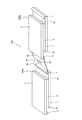
図1は、本発明の第1の実施形態に係る光電変換素子モジュールを示す断面図である。 FIG. 1 is a sectional view showing a photoelectric conversion element module according to the first embodiment of the present invention.
図1において、光電変換素子モジュール100は、2つの基板1上にそれぞれ設けられた光電変換素子100a、100bと、可とう性を有する平坦状のケーブル9とを備えており、光電変換素子100aと光電変換素子100bとは、ケーブル9によって電気的に接続されている。
In FIG. 1, a photoelectric
まず、基板1及び光電変換素子100a、100bについて説明するが、光電変換素子100aと光電変換素子100bは、同じ構成であるため、光電変換素子100aについてのみ説明する。
First, although the board |
本実施形態において、基板1は、透明な材料から構成されている。また、基板1を構成する材料は、電解液に対する耐性、及び、水蒸気、酸素等に対するガスバリア性に優れていることが好ましい。このような透明な材料は、可塑性のない材料として、ガラスを挙げることができ、可塑性のある材料として、ポリエチレンテレフタレート(PET)、ポリエチレンナフタレート(PEN)、ポリカーボネート(PC)、ポリエーテルスルフォン(PES)などの樹脂を挙げることができる。また、基板1は、ガラスと上記樹脂の積層体を用いて構成することもできる。
In the present embodiment, the
光電変換素子100aは、基板1上に設けられた透明電極となる透明導電層2と、透明導電層2と対向している対向電極5と、透明導電層2と対向電極5との間に設けられ、透明導電層2と対向基板5とに接触する光電変換部3と、透明電極層2と対向基板5とに接触し、光電変換部3を包囲するように設けられた封止材6とを主な構成要素として備えている。
The
透明導電層2は、基板1における光電変換部3が設けられる側の面の全面を覆うように設けられている。また、透明導電層2の光電変換部3側の面は、光電変換部3及び封止材6と接触する領域と、この領域の外側で光電変換部3及び封止材6と接触しない非接触領域25とを有している。
The transparent
透明導電層2は、光電変換部3で生じる電荷を集電し電送する機能を有し、また、光電変換部3に入射する光を透過する機能を有するため、導電性、光透過性の高い材料で形成されている。このような透明導電層2を構成する材料としては、例えばスズ添加酸化インジウム(Indium−Tin−Oxide:ITO)、酸化スズ(SnO2)、フッ素添加酸化スズ(Fluorine−Tin−Oxide:FTO)、アンチモン添加酸化スズ(Antimony−Tin−Oxide:ATO)などの導電性金属酸化物が挙げられる。透明導電層2は、単層でも、異なる導電性金属酸化物で構成される複数の層の積層体で構成されてもよく、複数の層で構成される積層体を用いると、各層の特性を反映させることが可能となることから好ましい。中でも、ITOで構成される層と、FTOで構成される層との積層体を用いることが好ましい。この場合、高い導電性、耐熱性及び耐薬品性を持つ透明導電層2が実現できる。
Since the transparent
透明導電層2を形成する方法としては、例えばスパッタ法、蒸着法、スプレー熱分解法(SPD:Spray Pyrolysis Deposition)及びCVD法などが挙げられる。中でも、スプレー熱分解法が短時間で容易に透明導電層2を形成できることから好ましい。透明導電層2の厚さは、例えば0.001μm〜10μmの範囲にすればよい。
Examples of the method for forming the transparent
対向電極5は、対向電極層52と、対向電極層52の光電変換部3とは反対側に設けられた対向電極基板51とを備える。また、対向電極5の光電変換部3側の面は、光電変換部3及び封止材6と接触する領域と、この領域の外側で光電変換部3及び封止材6と接触しない非接触領域55とを有する。具体的には、対向電極層52が、封止材6の外縁で囲まれる領域の直上の領域から、封止材6の外縁で囲まれる領域の直上の領域の外側まで延在している。
The
対向電極層52は、白金、チタン、炭素系材料、導電性高分子や、ITO、FTO、ATO等の導電性酸化物等の材料で構成することができる。
The
また、対向電極基板51は、対向電極基板51に導電性を持たせる場合には、チタン、ニッケル、金等の金属材料、ITO、FTO等の導電性酸化物、あるいは導電性高分子等で構成することができ、対向電極基板51に導電性を持たせる必要がない場合には、ガラス、PC、PET等で構成することができる。
Further, when the
さらに、対向電極層52及び対向電極基板51の双方に透明な材料を用いれば、対向電極5を透明とすることができる。この場合には、対向電極5側からも光を取り込むことができる。
Furthermore, if a transparent material is used for both the
なお、対向電極層52が十分な強度を保つことができれば、対向電極板51を省略することもでき、この場合、対向電極5が、対向電極層52のみから構成される。この場合、対向電極層52の材料としては、チタンや白金が用いられる。
If the
光電変換部3は、半導体層31と、半導体層31に担持される図示しない光増感色素と、半導体層31の周囲に設けられる電解質部32とを有している。
The
半導体層31は、透明導電層2上に設けられ、例えば酸化物半導体の粒子で構成される酸化物半導体多孔膜から成る。酸化物半導体の材料としては、例えば酸化チタン(TiO2)、酸化亜鉛(ZnO)、酸化タングステン(WO3)、酸化ニオブ(Nb2O5)、チタン酸ストロンチウム(SrTiO3)、酸化スズ(SnO2)、酸化インジウム(In3O3)、酸化ジルコニウム(ZrO2)、酸化タリウム(Ta2O5)、酸化ランタン(La2O3)、酸化イットリウム(Y2O3)、酸化ホスホニウム(Ho2O3)、酸化ビスマス(Bi2O3)、酸化セリウム(CeO2)、アルミナ(Al2O3)が挙げられ、これらの材料を1種用いたものでも良く、あるいは2種以上用いたものでも良い。2種類以上用いた場合には、粒子をコアシェル構造としても良い。
The
粒子の平均粒径としては、特に限定されるわけではないが、例えば1〜1000nmであることが必要な比表面積を確保するという理由から好ましい。また、半導体層31の厚さは、例えば0.5〜50μmであればよい。
Although it does not necessarily limit as an average particle diameter of particle | grains, it is preferable from the reason of ensuring the specific surface area which needs to be 1-1000 nm, for example. Moreover, the thickness of the
酸化物半導体多孔膜を形成するためには、例えば上記酸化物半導体粒子を塗布し、焼結させることにより得ることができる。 In order to form the oxide semiconductor porous film, for example, the oxide semiconductor particles can be applied and sintered.
光増感色素は、例えばビピリジン構造、ターピリジン構造などを含む配位子を有するルテニウム錯体や、エオシン、ローダミン、メロシアニンなどの有機色素が挙げられる。 Examples of the photosensitizing dye include a ruthenium complex having a ligand containing a bipyridine structure, a terpyridine structure, and the like, and organic dyes such as eosin, rhodamine, and merocyanine.
光増感色素を半導体層31に担持させるためには、例えば、光増感色素を含有する溶液を半導体層31に浸漬させることによって、光増感色素を酸化物半導体多孔膜に吸着させればよい。
In order to carry the photosensitizing dye on the
電解質部32は、例えば電解液となっており、電解液は、例えばI−/I3 −などの酸化還元対と有機溶媒とを含んでいる。有機溶媒としては、アセトニトリル、メトキシアセトニトリル、メトキシプロピオニトリル、エチレンカーボネート、プロピレンカーボネート、ジエチルカーボネート、γ−ブチロラクトンなどを用いることができる。酸化還元対としては、例えばI−/I3 −のほか、臭素/臭化物イオンなどの対であってもよい。
The
電解質部32としては、イオン液体電解質にSiO2、TiO2、カーボンナノチューブなどのナノ粒子を混練してゲル状となった擬固体電解質であるナノコンポジットイオンゲル電解質を用いてもよい。イオン液体電解質としては、例えば1−エチル−3−メチルイミダゾリウム ビス(トリフルオロメチルスルホニル)イミドに、1−エチル−3−メチルイミダゾリウムヨーダイド、LiI、I2、4−t−ブチルピリジンを所定量溶解したものなどが挙げられる。
As the
電解質部32を半導体層31の周囲に設ける方法としては、電解質部32が電解液である場合には、半導体層31に対向するように対向電極5を配置し、対向電極5の周囲を封止材6で封止した後、封止材6に形成した電解液を注入するための注入口を通して電解液を注入する方法が挙げられる。また、電解質部13が上記ナノコンポジットイオンゲル電解質である場合には、上記ナノコンポジットイオンゲル電解質を含むペーストを用意し、これを例えばスクリーン印刷法等によって塗布する方法が挙げられる。
As a method of providing the
上記電解質層の厚さは、特に限定されるものではないが、例えば、50μm以下であれば、電解液の電気抵抗が抑えられるという理由から好ましい。 The thickness of the electrolyte layer is not particularly limited. For example, a thickness of 50 μm or less is preferable because the electrical resistance of the electrolytic solution can be suppressed.
封止材6は、電解質部32に対する耐性が必要であるため耐薬品性に優れ、また、水蒸気、酸素等に対するガスバリア性に優れた材料が好ましい。このような、封止材6の材料としては、例えば、アクリル系樹脂封止材、フッ素系樹脂封止材、シリコーン系樹脂封止材、エポキシ系樹脂封止材、オレフィン系樹脂封止材、シラン変性樹脂含有封止材、ホットメルト系封止材等を用いることができる。
Since the sealing
透明導電層2の光電変換部3側の面における非接触領域25には、端子7が設けられている。端子7は、導電層71とはんだ層72から構成されている。導電層71は、金、銀、銅、白金、アルミニウム等の金属を用いて構成することができる。導電層71は、例えば、銀ペーストを印刷により塗布し、加熱・反応させて形成すればよい。また、はんだ層72は、例えば、Sn−Pb等の共晶タイプや、Sn−Ag、Sn−Cu、An−Ag−Cu、An−Zn、Sn−Zn−B等の非鉛タイプの低融点はんだを用いて構成することができる。
A
対向電極層52の光電変換部3側の面における非接触領域55には、端子8が設けられている。端子8は、導電層81とはんだ層82とから構成され、導電層81が対向電極層52上に設けられており、導電層81上に、はんだ層82が形成されている。導電層81の材料は、対向電極層52の材料により異なるが、対向電極層52が、白金、チタンの場合には、高融点はんだが用いられる。対向電極層52が、ITO、FTO、ATO等の導電性酸化物の場合には、導電層71と同様の材料が用いられる。はんだ層82は、低融点はんだで形成されている。
A
次に、光電変換素子モジュール100について説明する。
Next, the photoelectric
光電変換素子モジュール100は、光電変換素子100bから光電変換素子100aに電流が流れるように、光電変換素子100aと光電変換素子100bとが、ケーブル9により電気的に直列に接続されている。具体的には、ケーブル9の一端が光電変換素子100aの端子7に接続され、ケーブル9の他端が光電変換素子100bの端子8に接続されている。
In the photoelectric
ケーブル9には、銅等の導体箔をラミネート材で挟んでいるFPC(Flexible Printed Circuit)や、極細のケーブルを複数平面状に束ねたフラットケーブルアセンブリ等を用いることができる。
The
なお、光電変換素子100aの端子8及び光電変換素子100bの端子7は、図示しない負荷と接続される。
Note that the
本実施形態の光電変換素子モジュール100によれば、光電変換素子モジュール100の2つの光電変換素子100a、100bが、2つの基板1上にそれぞれ設けられて、可とう性を有する平坦状のケーブル9により電気的に接続されている。このため、例えば、複数の平面が互いに段差を介して並んでいる階段状の設置場所に光電変換素子モジュール100を配置する際、設置場所の段差に応じてケーブル9が撓み、設置場所の各平面に光電変換素子100a、100bが設けられた各基板1が配置できる。従って、設置場所に応じた専用の設置用器具等を用いず、容易に光電変換素子モジュール100を設置場所に設置することができる。
According to the photoelectric
この効果について、図2を用いて具体的に説明する。図2は、光電変換素子モジュール100を部材S上に設置する状態を示す斜視図である。部材Sは、例えば屋根の一部等であり、階段状の形状をしている。部材Sは、段差Stを介して並んでいる2つの平面S1とS2とを有している。そして、光電変換素子100aが平面S1上に配置され、光電変換素子100bが平面S2上に配置される。
This effect will be specifically described with reference to FIG. FIG. 2 is a perspective view showing a state in which the photoelectric
この際、各光電変換素子100a、100bは、基板1側から光を取りこんで、光電変換部3で光電変換を行うため、基板1が平面S1、S2とは反対側を向いて設置される。
At this time, each
光電変換素子100a、100bは、可とう性を有する平坦状のケーブル9により接続されているため、ケーブル9が、段差Stの高さに合わせて撓んだ状態で、光電変換素子100a、100bが、それぞれ平面S1、S2に配置される。このようにケーブル9の撓みが、段差Stによる平面S1と平面S2の高さの差を吸収する。このため、段差Stの高さに応じた専用の設置用器具等を用いず、光電変換素子モジュール100を部材S上に設置することができる。
Since the
また、各光電変換素子100a、100bは、平坦状のケーブル9で接続されているので、通常のケーブルを用いて接続した場合に比べて、ケーブル9と光電変換素子100a、100bに設けられた端子7、8との接続幅が大きい。さらに、光電変換素子100a、100bは、非接触領域25、55を有し、ケーブル9が、非接触領域25、55で電気的に接続されているため、非接触領域25、55にケーブル9との十分な接続面積を確保できる。このため、光電変換素子100a、100bとケーブル9との接続による電気的な抵抗が小さく、光電変換素子モジュール100の内部抵抗を軽減でき、光電変換素子モジュール100の光電変換効率を向上できる。また、ケーブル9と各光電変換素子100a、100bとの電気的な接続作業が容易である。
Moreover, since each
また、光電変換素子100aは、透明電極層2の光電変換部3側の非接触領域25に設けられた端子7とケーブル9とが電気的に接続され、光電変換素子100bは、対向電極5の光電変換部3側の非接触領域55に設けられた端子8とケーブル9とが電気的に接続されている。このため、部材Sに光電変換素子モジュール100を設置する際、ケーブル9は、光電変換素子モジュール100と部材Sとの間に入り込み邪魔になることがない。
従って、容易に光電変換素子モジュール100を部材Sに設置することができる。
In the
Therefore, the photoelectric
また、各光電変換素子100a、100bを平坦状のケーブル9で接続しているので、ケーブル9上に、光電変換素子モジュールを制御する電子部品等を配置することができる。
Moreover, since each
(第2の実施形態) (Second Embodiment)
図3は、本発明の第2の実施形態に係る光電変換素子モジュールを示す断面図である。なお、本実施形態の説明に当たり、第1の実施形態と同一または同等の構成要素には、同一の符号を付し、重複する説明を省略する。 FIG. 3 is a cross-sectional view showing a photoelectric conversion element module according to the second embodiment of the present invention. In the description of the present embodiment, the same or equivalent components as those in the first embodiment are denoted by the same reference numerals, and redundant description is omitted.
図3に示すように、本実施形態の光電変換素子モジュール101は、2つの基板1上に設けられた光電変換素子100c、100dとケーブル9とを備えている。なお、光電変換素子100cと光電変換素子100dは、同じ構成であるため、光電変換素子100cについてのみ説明を行う。
As shown in FIG. 3, the photoelectric
光電変換素子100cの対向電極58は、対向電極層54と、対向電極層54の光電変換部3とは反対側に設けられた対向電極基板53とを備える。対向電極58の光電変換部3側の面は、光電変換部3及び封止材6と接触する領域の外側の領域を有しておらず、対向電極58は、封止材6の外周で囲まれる領域の直上の領域のみに設けられている。また、端子8が対向電極58の光電変換部3とは反対側、すなわち光電変換素子100cの上側に設けられている。このため、対向電極58の対向電極基板53は、導電性の材料を用いて構成されている。導電性の材料としては、チタン、ニッケル、金等の金属材料やITO、FTO等の導電性酸化物等が挙げられる。
The
本実施形態の光電変換素子モジュール101によれば、ケーブル9が、対向電極58の光電変換部の反対側の面で光電変換素子100dと電気的に接続されているため、封止材6が透明導電層2及び対向電極58と接触し光電変換部3を包囲する限りにおいては、対向電極58の大きさを自由に構成することができる。このため、対向電極58は、封止材6で包囲された領域の直上の領域のみに設けられる構成とすることができる。このため対向電極58の小型化ができ、従って光電変換素子モジュール101の小型化ができる。
According to the photoelectric
(第3の実施形態) (Third embodiment)
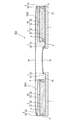
図4は、本発明の第3の実施形態に係る光電変換素子モジュールを示す斜視図である。なお、本実施形態の説明に当たり、第1の実施形態と同一または同等の構成要素には、同一の符号を付し、重複する説明を省略する。 FIG. 4 is a perspective view showing a photoelectric conversion element module according to the third embodiment of the present invention. In the description of the present embodiment, the same or equivalent components as those in the first embodiment are denoted by the same reference numerals, and redundant description is omitted.
図4において、光電変換素子モジュール102は、光電変換素子100bから光電変換素子100aに電流が流れるように、光電変換素子100a、100bが、可とう性を有する平坦状のケーブル94で電気的に接続されている。ケーブル94としては、例えばFPCが用いられる。
In FIG. 4, in the photoelectric
本実施形態では、ケーブル94上の略中心に電子部品としてダイオード95が配置されている。図3において、ケーブル94の導体9a、9bは、波線で示されており、導体9aが、光電変換素子100aと接続され、導体9bが光電変換素子100bと接続されている。また、ダイオード95の幅は、ケーブル94の幅に比べ小さいため、導体9a、9bの幅は、ダイオード95側が狭く、光電変換素子100a、100b側が広くなっている。また、光電変換素子100bから光電変換素子100aに電流が流れるため、ダイオード95は、アノードが導体9bに接続され、カソードが導体9aに接続されている。
In the present embodiment, a
ダイオード95を設けることにより、光電変換素子100aの電位が、光電変換素子100bの電位よりも高くなったとしても、電流が光電変換素子100aから光電変換素子100bに逆流することが防止できる。
By providing the
本実施形態の光電変換素子モジュール102によれば、電流等を制御する電子部品がケーブル上に配置されているため、電子部品を配置するために光電変換素子モジュール102の他にプリント配線板等を設ける必要がない。
According to the photoelectric
以上、本発明の好適な実施形態を第1、第2、第3の実施形態を用いて説明したが、本発明は、これに限らず種々の変形が可能である。 As mentioned above, although preferred embodiment of this invention was described using 1st, 2nd, 3rd embodiment, this invention is not restricted to this, A various deformation | transformation is possible.
例えば、第1、第2の実施形態では、各光電変換素子を電気的に直列に接続した例について説明をしたが、第1、第2の実施形態について、光電変換素子を電気的に並列に接続した構成としても良い。 For example, in the first and second embodiments, the example in which the photoelectric conversion elements are electrically connected in series has been described. However, in the first and second embodiments, the photoelectric conversion elements are electrically connected in parallel. A connected configuration may be used.
図5は、光電変換素子同士が電気的に並列に接続された光電変換素子モジュールを示す断面図である。図5においては、本発明の第2の実施形態で説明した光電変換素子100c、100dが電気的に並列に接続されている。
FIG. 5 is a cross-sectional view showing a photoelectric conversion element module in which photoelectric conversion elements are electrically connected in parallel. In FIG. 5, the
図5に示すように、本実施形態の光電変換素子モジュール103は、光電変換素子100cの端子8と光電変換素子100dの端子8とが、可とう性を有する平坦状のケーブル91で接続され、光電変換素子100cの端子7と光電変換素子100dの端子7とが、可とう性を有する平坦状のケーブル92で接続されている。
As shown in FIG. 5, in the photoelectric
光電変換素子モジュール103と負荷とを接続する場合は、例えば、光電変換素子100cの端子8と光電変換素子100dの端子7とを負荷に接続すればよい。
When connecting the photoelectric
また、各実施形態において、光電変換素子が、2つ接続された例を示したが、本発明は、これに限らず3つ以上の光電変換素子を接続しても良い。 Moreover, in each embodiment, although the example to which two photoelectric conversion elements were connected was shown, this invention is not restricted to this, You may connect three or more photoelectric conversion elements.
また、各実施形態において、光電変換素子モジュールが、色素増感型の光電変換素子を用いた光電変換素子モジュールを例として説明をしたが、本発明はこれに限らず、例えば、シリコン系の光電変換素子や、薄膜系の光電変換素子を用いた光電変換素子モジュールであっても良い。 Moreover, in each embodiment, although the photoelectric conversion element module demonstrated the photoelectric conversion element module using the dye-sensitized photoelectric conversion element as an example, this invention is not limited to this, For example, a silicon type photoelectric conversion element A photoelectric conversion element module using a conversion element or a thin film photoelectric conversion element may be used.
その他、基板1、透明導電層2、光電変換部3、対向電極5、ケーブル9等の各材料、構成等は、本発明の課題を解決する範囲で種々変更が可能である。
In addition, the materials, configurations, and the like of the
100,101,102,103・・・光電変換素子モジュール、100a,100b,100c,100d・・・光電変換素子、1・・・基板、2・・・透明導電層、3・・・光電変換部、31・・・半導体層、32・・・電解質部、5,58・・・対向電極、51,53・・・対向電極基板、52,54・・・対向電極層、6・・・封止材、7,8・・・端子、9,91,92,94・・・ケーブル、95・・・ダイオード
DESCRIPTION OF SYMBOLS 100,101,102,103 ... Photoelectric conversion element module, 100a, 100b, 100c, 100d ... Photoelectric conversion element, 1 ... Substrate, 2 ... Transparent conductive layer, 3 ...
Claims (3)
前記複数の基板のそれぞれに設けられた光電変換素子とを備え、
前記光電変換素子同士は、可とう性を有する平坦状のケーブルで電気的に接続されること
を特徴とする光電変換素子モジュール。 Multiple substrates;
A photoelectric conversion element provided on each of the plurality of substrates,
The photoelectric conversion elements are electrically connected to each other by a flat cable having flexibility.
前記光電変換素子の少なくとも一つは、前記一対の電極の少なくとも一方における前記光電変換部側の面が、前記封止材と接触する領域の外側に非接触領域を有し、
前記ケーブルの一端は、前記光電変換素子の前記非接触領域と電気的に接続されること
を特徴とする請求項1に記載の光電変換素子モジュール。 The photoelectric conversion element includes a pair of electrodes, a photoelectric conversion unit provided between the pair of electrodes and in contact with each electrode, and a sealing material that contacts the pair of electrodes and surrounds the photoelectric conversion unit. ,
At least one of the photoelectric conversion elements has a non-contact region outside the region in which the surface on the photoelectric conversion unit side in at least one of the pair of electrodes is in contact with the sealing material,
The photoelectric conversion element module according to claim 1, wherein one end of the cable is electrically connected to the non-contact region of the photoelectric conversion element.
前記ケーブルの一端は、少なくとも前記光電変換素子の1つにおいて、前記一対の電極の一方における前記光電変換部と反対側の面で前記光電変換素子と電気的に接続されること
を特徴とする請求項1に記載の光電変換素子モジュール。
The photoelectric conversion element includes a pair of electrodes, a photoelectric conversion unit provided between the pair of electrodes and in contact with each electrode, and a sealing material that contacts the pair of electrodes and surrounds the photoelectric conversion unit. ,
One end of the cable is electrically connected to the photoelectric conversion element on a surface opposite to the photoelectric conversion unit in one of the pair of electrodes in at least one of the photoelectric conversion elements. Item 2. The photoelectric conversion element module according to Item 1.
Priority Applications (1)
| Application Number | Priority Date | Filing Date | Title |
|---|---|---|---|
| JP2008180366A JP5324147B2 (en) | 2008-07-10 | 2008-07-10 | Photoelectric conversion element module |
Applications Claiming Priority (1)
| Application Number | Priority Date | Filing Date | Title |
|---|---|---|---|
| JP2008180366A JP5324147B2 (en) | 2008-07-10 | 2008-07-10 | Photoelectric conversion element module |
Publications (2)
| Publication Number | Publication Date |
|---|---|
| JP2010021013A true JP2010021013A (en) | 2010-01-28 |
| JP5324147B2 JP5324147B2 (en) | 2013-10-23 |
Family
ID=41705699
Family Applications (1)
| Application Number | Title | Priority Date | Filing Date |
|---|---|---|---|
| JP2008180366A Expired - Fee Related JP5324147B2 (en) | 2008-07-10 | 2008-07-10 | Photoelectric conversion element module |
Country Status (1)
| Country | Link |
|---|---|
| JP (1) | JP5324147B2 (en) |
Cited By (4)
| Publication number | Priority date | Publication date | Assignee | Title |
|---|---|---|---|---|
| JP2014053111A (en) * | 2012-09-05 | 2014-03-20 | Fujikura Ltd | Dye-sensitized solar cell module |
| JP2016204533A (en) * | 2015-04-23 | 2016-12-08 | ダイキン工業株式会社 | Coating composition |
| WO2019188433A1 (en) * | 2018-03-30 | 2019-10-03 | 日本ゼオン株式会社 | Environmental power generator |
| JP2020128560A (en) * | 2020-06-03 | 2020-08-27 | ダイキン工業株式会社 | Coating composition |
Citations (1)
| Publication number | Priority date | Publication date | Assignee | Title |
|---|---|---|---|---|
| JP2006057321A (en) * | 2004-08-19 | 2006-03-02 | Mitsubishi Heavy Ind Ltd | Solar battery panel and construction method of the same |
-
2008
- 2008-07-10 JP JP2008180366A patent/JP5324147B2/en not_active Expired - Fee Related
Patent Citations (1)
| Publication number | Priority date | Publication date | Assignee | Title |
|---|---|---|---|---|
| JP2006057321A (en) * | 2004-08-19 | 2006-03-02 | Mitsubishi Heavy Ind Ltd | Solar battery panel and construction method of the same |
Cited By (6)
| Publication number | Priority date | Publication date | Assignee | Title |
|---|---|---|---|---|
| JP2014053111A (en) * | 2012-09-05 | 2014-03-20 | Fujikura Ltd | Dye-sensitized solar cell module |
| JP2016204533A (en) * | 2015-04-23 | 2016-12-08 | ダイキン工業株式会社 | Coating composition |
| WO2019188433A1 (en) * | 2018-03-30 | 2019-10-03 | 日本ゼオン株式会社 | Environmental power generator |
| JPWO2019188433A1 (en) * | 2018-03-30 | 2021-04-22 | 日本ゼオン株式会社 | Energy harvester |
| JP7327381B2 (en) | 2018-03-30 | 2023-08-16 | 日本ゼオン株式会社 | energy generator |
| JP2020128560A (en) * | 2020-06-03 | 2020-08-27 | ダイキン工業株式会社 | Coating composition |
Also Published As
| Publication number | Publication date |
|---|---|
| JP5324147B2 (en) | 2013-10-23 |
Similar Documents
| Publication | Publication Date | Title |
|---|---|---|
| JP4854971B2 (en) | Dye-sensitized solar cell module | |
| US10096431B2 (en) | Dye-sensitized solar cell element for low illuminance | |
| JP2006324090A (en) | Photoelectric conversion module and photovoltaic generator using it | |
| US10020121B2 (en) | Dye-sensitized photoelectric conversion element | |
| KR100384893B1 (en) | Nano-particle oxide solar cells and fabrication method of the same and solar cell modules and transparent electric window using the same | |
| JP5324147B2 (en) | Photoelectric conversion element module | |
| JP5451920B1 (en) | Dye-sensitized solar cell element | |
| JP6122156B2 (en) | Photoelectric conversion element | |
| JP2014130807A (en) | Dye-sensitized solar cell module | |
| US9589736B2 (en) | Dye-sensitized solar cell element | |
| JP2015056294A (en) | Dye-sensitized solar cell element | |
| JP2007227260A (en) | Photoelectric converter and photovoltaic generator | |
| JP5996995B2 (en) | Dye-sensitized solar cell and dye-sensitized solar cell module | |
| JP5680996B2 (en) | Dye-sensitized solar cell module and manufacturing method thereof | |
| WO2018092741A1 (en) | Photoelectric conversion element | |
| JP5013741B2 (en) | Photoelectric conversion device and photovoltaic power generation device | |
| JP6573497B2 (en) | Photoelectric conversion element | |
| US10008336B2 (en) | Dye-sensitized solar cell element | |
| CN107615425B (en) | Photoelectric conversion element | |
| JP5969865B2 (en) | Dye-sensitized solar cell module | |
| JP6598757B2 (en) | Photoelectric conversion element | |
| JP6694371B2 (en) | Photoelectric conversion element | |
| JP6697335B2 (en) | Photoelectric conversion element | |
| JP6006075B2 (en) | Dye-sensitized solar cell and dye-sensitized solar cell module | |
| WO2018092740A1 (en) | Photoelectric conversion element |
Legal Events
| Date | Code | Title | Description |
|---|---|---|---|
| A621 | Written request for application examination |
Free format text: JAPANESE INTERMEDIATE CODE: A621 Effective date: 20110610 |
|
| A131 | Notification of reasons for refusal |
Free format text: JAPANESE INTERMEDIATE CODE: A131 Effective date: 20130426 |
|
| A521 | Request for written amendment filed |
Free format text: JAPANESE INTERMEDIATE CODE: A523 Effective date: 20130620 |
|
| TRDD | Decision of grant or rejection written | ||
| A01 | Written decision to grant a patent or to grant a registration (utility model) |
Free format text: JAPANESE INTERMEDIATE CODE: A01 Effective date: 20130709 |
|
| A61 | First payment of annual fees (during grant procedure) |
Free format text: JAPANESE INTERMEDIATE CODE: A61 Effective date: 20130718 |
|
| R150 | Certificate of patent or registration of utility model |
Ref document number: 5324147 Country of ref document: JP Free format text: JAPANESE INTERMEDIATE CODE: R150 Free format text: JAPANESE INTERMEDIATE CODE: R150 |
|
| R250 | Receipt of annual fees |
Free format text: JAPANESE INTERMEDIATE CODE: R250 |
|
| R250 | Receipt of annual fees |
Free format text: JAPANESE INTERMEDIATE CODE: R250 |
|
| R250 | Receipt of annual fees |
Free format text: JAPANESE INTERMEDIATE CODE: R250 |
|
| R250 | Receipt of annual fees |
Free format text: JAPANESE INTERMEDIATE CODE: R250 |
|
| R250 | Receipt of annual fees |
Free format text: JAPANESE INTERMEDIATE CODE: R250 |
|
| R250 | Receipt of annual fees |
Free format text: JAPANESE INTERMEDIATE CODE: R250 |
|
| R250 | Receipt of annual fees |
Free format text: JAPANESE INTERMEDIATE CODE: R250 |
|
| LAPS | Cancellation because of no payment of annual fees |