JP2010019766A - Detection method, detector, detecting sample cell and detecting kit - Google Patents
Detection method, detector, detecting sample cell and detecting kit Download PDFInfo
- Publication number
- JP2010019766A JP2010019766A JP2008182226A JP2008182226A JP2010019766A JP 2010019766 A JP2010019766 A JP 2010019766A JP 2008182226 A JP2008182226 A JP 2008182226A JP 2008182226 A JP2008182226 A JP 2008182226A JP 2010019766 A JP2010019766 A JP 2010019766A
- Authority
- JP
- Japan
- Prior art keywords
- substance
- fluorescent
- fluorescent label
- detected
- excitation
- Prior art date
- Legal status (The legal status is an assumption and is not a legal conclusion. Google has not performed a legal analysis and makes no representation as to the accuracy of the status listed.)
- Granted
Links
- 238000001514 detection method Methods 0.000 title claims abstract description 123
- 239000000126 substance Substances 0.000 claims abstract description 280
- 239000007850 fluorescent dye Substances 0.000 claims abstract description 155
- 230000005284 excitation Effects 0.000 claims abstract description 134
- 239000007788 liquid Substances 0.000 claims abstract description 69
- 239000000463 material Substances 0.000 claims abstract description 38
- 239000002184 metal Substances 0.000 claims description 199
- 229910052751 metal Inorganic materials 0.000 claims description 199
- 230000003287 optical effect Effects 0.000 claims description 95
- 230000005684 electric field Effects 0.000 claims description 31
- 238000002372 labelling Methods 0.000 claims description 22
- 239000002245 particle Substances 0.000 claims description 20
- 239000000243 solution Substances 0.000 claims description 19
- 238000002347 injection Methods 0.000 claims description 12
- 239000007924 injection Substances 0.000 claims description 12
- 125000000524 functional group Chemical group 0.000 claims description 11
- 238000011144 upstream manufacturing Methods 0.000 claims description 10
- 230000001678 irradiating effect Effects 0.000 claims description 8
- NNJPGOLRFBJNIW-HNNXBMFYSA-N (-)-demecolcine Chemical compound C1=C(OC)C(=O)C=C2[C@@H](NC)CCC3=CC(OC)=C(OC)C(OC)=C3C2=C1 NNJPGOLRFBJNIW-HNNXBMFYSA-N 0.000 abstract description 53
- OMOVVBIIQSXZSZ-UHFFFAOYSA-N [6-(4-acetyloxy-5,9a-dimethyl-2,7-dioxo-4,5a,6,9-tetrahydro-3h-pyrano[3,4-b]oxepin-5-yl)-5-formyloxy-3-(furan-3-yl)-3a-methyl-7-methylidene-1a,2,3,4,5,6-hexahydroindeno[1,7a-b]oxiren-4-yl] 2-hydroxy-3-methylpentanoate Chemical compound CC12C(OC(=O)C(O)C(C)CC)C(OC=O)C(C3(C)C(CC(=O)OC4(C)COC(=O)CC43)OC(C)=O)C(=C)C32OC3CC1C=1C=COC=1 OMOVVBIIQSXZSZ-UHFFFAOYSA-N 0.000 abstract description 11
- 230000035945 sensitivity Effects 0.000 abstract description 2
- 238000004040 coloring Methods 0.000 abstract 2
- 238000000034 method Methods 0.000 description 71
- 238000005259 measurement Methods 0.000 description 65
- 210000004027 cell Anatomy 0.000 description 58
- 101710098119 Chaperonin GroEL 2 Proteins 0.000 description 31
- 210000004369 blood Anatomy 0.000 description 31
- 239000008280 blood Substances 0.000 description 31
- 239000010931 gold Substances 0.000 description 28
- 238000001917 fluorescence detection Methods 0.000 description 27
- 230000000694 effects Effects 0.000 description 26
- 239000000427 antigen Substances 0.000 description 19
- 102000036639 antigens Human genes 0.000 description 18
- 108091007433 antigens Proteins 0.000 description 18
- 238000003556 assay Methods 0.000 description 18
- 229910052737 gold Inorganic materials 0.000 description 18
- PCHJSUWPFVWCPO-UHFFFAOYSA-N gold Chemical compound [Au] PCHJSUWPFVWCPO-UHFFFAOYSA-N 0.000 description 15
- 239000000758 substrate Substances 0.000 description 15
- 125000003178 carboxy group Chemical group [H]OC(*)=O 0.000 description 13
- 239000013076 target substance Substances 0.000 description 13
- 239000004793 Polystyrene Substances 0.000 description 11
- 238000010586 diagram Methods 0.000 description 11
- 239000012528 membrane Substances 0.000 description 11
- 229920002223 polystyrene Polymers 0.000 description 11
- 238000006243 chemical reaction Methods 0.000 description 10
- 230000002860 competitive effect Effects 0.000 description 8
- 238000002198 surface plasmon resonance spectroscopy Methods 0.000 description 8
- 230000008859 change Effects 0.000 description 7
- 239000002073 nanorod Substances 0.000 description 7
- 230000005855 radiation Effects 0.000 description 7
- 239000010419 fine particle Substances 0.000 description 6
- 238000002795 fluorescence method Methods 0.000 description 6
- 230000001965 increasing effect Effects 0.000 description 6
- 238000010791 quenching Methods 0.000 description 6
- 230000000171 quenching effect Effects 0.000 description 6
- 238000013461 design Methods 0.000 description 5
- LOKCTEFSRHRXRJ-UHFFFAOYSA-I dipotassium trisodium dihydrogen phosphate hydrogen phosphate dichloride Chemical compound P(=O)(O)(O)[O-].[K+].P(=O)(O)([O-])[O-].[Na+].[Na+].[Cl-].[K+].[Cl-].[Na+] LOKCTEFSRHRXRJ-UHFFFAOYSA-I 0.000 description 5
- 230000002708 enhancing effect Effects 0.000 description 5
- 239000002953 phosphate buffered saline Substances 0.000 description 5
- 230000009471 action Effects 0.000 description 4
- 238000000576 coating method Methods 0.000 description 4
- 210000003743 erythrocyte Anatomy 0.000 description 4
- 230000003100 immobilizing effect Effects 0.000 description 4
- 150000004706 metal oxides Chemical class 0.000 description 4
- 230000008569 process Effects 0.000 description 4
- 238000001179 sorption measurement Methods 0.000 description 4
- 230000005653 Brownian motion process Effects 0.000 description 3
- XEKOWRVHYACXOJ-UHFFFAOYSA-N Ethyl acetate Chemical compound CCOC(C)=O XEKOWRVHYACXOJ-UHFFFAOYSA-N 0.000 description 3
- 229920002873 Polyethylenimine Polymers 0.000 description 3
- 229910045601 alloy Inorganic materials 0.000 description 3
- 239000000956 alloy Substances 0.000 description 3
- 229910052782 aluminium Inorganic materials 0.000 description 3
- 238000007743 anodising Methods 0.000 description 3
- 210000000601 blood cell Anatomy 0.000 description 3
- 238000005537 brownian motion Methods 0.000 description 3
- 239000011248 coating agent Substances 0.000 description 3
- 229910052802 copper Inorganic materials 0.000 description 3
- 238000009826 distribution Methods 0.000 description 3
- 150000002605 large molecules Chemical class 0.000 description 3
- 210000000265 leukocyte Anatomy 0.000 description 3
- 230000031700 light absorption Effects 0.000 description 3
- 229920002521 macromolecule Polymers 0.000 description 3
- 229910044991 metal oxide Inorganic materials 0.000 description 3
- 239000002923 metal particle Substances 0.000 description 3
- 239000002105 nanoparticle Substances 0.000 description 3
- 229910052759 nickel Inorganic materials 0.000 description 3
- 238000007747 plating Methods 0.000 description 3
- 229910052697 platinum Inorganic materials 0.000 description 3
- 239000000376 reactant Substances 0.000 description 3
- 230000002829 reductive effect Effects 0.000 description 3
- 210000002966 serum Anatomy 0.000 description 3
- 229910052709 silver Inorganic materials 0.000 description 3
- 239000006228 supernatant Substances 0.000 description 3
- 230000005469 synchrotron radiation Effects 0.000 description 3
- 229910052719 titanium Inorganic materials 0.000 description 3
- 229910001111 Fine metal Inorganic materials 0.000 description 2
- DHMQDGOQFOQNFH-UHFFFAOYSA-N Glycine Chemical compound NCC(O)=O DHMQDGOQFOQNFH-UHFFFAOYSA-N 0.000 description 2
- 125000003277 amino group Chemical group 0.000 description 2
- 239000007864 aqueous solution Substances 0.000 description 2
- 230000002238 attenuated effect Effects 0.000 description 2
- 238000005119 centrifugation Methods 0.000 description 2
- 230000008878 coupling Effects 0.000 description 2
- 238000010168 coupling process Methods 0.000 description 2
- 238000005859 coupling reaction Methods 0.000 description 2
- 230000007423 decrease Effects 0.000 description 2
- 238000001125 extrusion Methods 0.000 description 2
- 238000001506 fluorescence spectroscopy Methods 0.000 description 2
- 230000001939 inductive effect Effects 0.000 description 2
- 238000004519 manufacturing process Methods 0.000 description 2
- 229920000767 polyaniline Polymers 0.000 description 2
- 239000000047 product Substances 0.000 description 2
- 102000004169 proteins and genes Human genes 0.000 description 2
- 108090000623 proteins and genes Proteins 0.000 description 2
- 239000011347 resin Substances 0.000 description 2
- 229920005989 resin Polymers 0.000 description 2
- 239000004065 semiconductor Substances 0.000 description 2
- 239000007787 solid Substances 0.000 description 2
- 239000002904 solvent Substances 0.000 description 2
- 125000006850 spacer group Chemical group 0.000 description 2
- 239000012798 spherical particle Substances 0.000 description 2
- 238000003756 stirring Methods 0.000 description 2
- 238000012546 transfer Methods 0.000 description 2
- 238000007740 vapor deposition Methods 0.000 description 2
- 238000005406 washing Methods 0.000 description 2
- 229910018072 Al 2 O 3 Inorganic materials 0.000 description 1
- 102000009027 Albumins Human genes 0.000 description 1
- 108010088751 Albumins Proteins 0.000 description 1
- 229920002307 Dextran Polymers 0.000 description 1
- 239000004471 Glycine Substances 0.000 description 1
- ZRALSGWEFCBTJO-UHFFFAOYSA-N Guanidine Chemical group NC(N)=N ZRALSGWEFCBTJO-UHFFFAOYSA-N 0.000 description 1
- 239000007987 MES buffer Substances 0.000 description 1
- NBIIXXVUZAFLBC-UHFFFAOYSA-N Phosphoric acid Chemical group OP(O)(O)=O NBIIXXVUZAFLBC-UHFFFAOYSA-N 0.000 description 1
- 229910004298 SiO 2 Inorganic materials 0.000 description 1
- VYPSYNLAJGMNEJ-UHFFFAOYSA-N Silicium dioxide Chemical compound O=[Si]=O VYPSYNLAJGMNEJ-UHFFFAOYSA-N 0.000 description 1
- 230000004308 accommodation Effects 0.000 description 1
- 238000002048 anodisation reaction Methods 0.000 description 1
- 239000011230 binding agent Substances 0.000 description 1
- 230000015572 biosynthetic process Effects 0.000 description 1
- 239000000872 buffer Substances 0.000 description 1
- 239000007853 buffer solution Substances 0.000 description 1
- 239000003054 catalyst Substances 0.000 description 1
- 239000000084 colloidal system Substances 0.000 description 1
- 239000004020 conductor Substances 0.000 description 1
- 230000003247 decreasing effect Effects 0.000 description 1
- 239000003989 dielectric material Substances 0.000 description 1
- 238000009792 diffusion process Methods 0.000 description 1
- 238000007599 discharging Methods 0.000 description 1
- BFMYDTVEBKDAKJ-UHFFFAOYSA-L disodium;(2',7'-dibromo-3',6'-dioxido-3-oxospiro[2-benzofuran-1,9'-xanthene]-4'-yl)mercury;hydrate Chemical compound O.[Na+].[Na+].O1C(=O)C2=CC=CC=C2C21C1=CC(Br)=C([O-])C([Hg])=C1OC1=C2C=C(Br)C([O-])=C1 BFMYDTVEBKDAKJ-UHFFFAOYSA-L 0.000 description 1
- 239000000975 dye Substances 0.000 description 1
- 238000002848 electrochemical method Methods 0.000 description 1
- 238000007772 electroless plating Methods 0.000 description 1
- 238000001704 evaporation Methods 0.000 description 1
- 238000001215 fluorescent labelling Methods 0.000 description 1
- 239000011521 glass Substances 0.000 description 1
- 125000002883 imidazolyl group Chemical group 0.000 description 1
- 238000007689 inspection Methods 0.000 description 1
- 239000007791 liquid phase Substances 0.000 description 1
- 230000004807 localization Effects 0.000 description 1
- 238000000691 measurement method Methods 0.000 description 1
- 230000007246 mechanism Effects 0.000 description 1
- 239000007769 metal material Substances 0.000 description 1
- 150000002739 metals Chemical class 0.000 description 1
- 239000004005 microsphere Substances 0.000 description 1
- 102000039446 nucleic acids Human genes 0.000 description 1
- 108020004707 nucleic acids Proteins 0.000 description 1
- 150000007523 nucleic acids Chemical class 0.000 description 1
- 239000003921 oil Substances 0.000 description 1
- 230000033116 oxidation-reduction process Effects 0.000 description 1
- 238000012856 packing Methods 0.000 description 1
- 229920000128 polypyrrole Polymers 0.000 description 1
- 125000001453 quaternary ammonium group Chemical group 0.000 description 1
- 230000035484 reaction time Effects 0.000 description 1
- 238000011160 research Methods 0.000 description 1
- 238000007788 roughening Methods 0.000 description 1
- 229910052814 silicon oxide Inorganic materials 0.000 description 1
- 125000000542 sulfonic acid group Chemical group 0.000 description 1
- 238000012360 testing method Methods 0.000 description 1
- 239000002699 waste material Substances 0.000 description 1
Images


Classifications
-
- G—PHYSICS
- G01—MEASURING; TESTING
- G01N—INVESTIGATING OR ANALYSING MATERIALS BY DETERMINING THEIR CHEMICAL OR PHYSICAL PROPERTIES
- G01N21/00—Investigating or analysing materials by the use of optical means, i.e. using sub-millimetre waves, infrared, visible or ultraviolet light
- G01N21/62—Systems in which the material investigated is excited whereby it emits light or causes a change in wavelength of the incident light
- G01N21/63—Systems in which the material investigated is excited whereby it emits light or causes a change in wavelength of the incident light optically excited
- G01N21/64—Fluorescence; Phosphorescence
- G01N21/645—Specially adapted constructive features of fluorimeters
- G01N21/648—Specially adapted constructive features of fluorimeters using evanescent coupling or surface plasmon coupling for the excitation of fluorescence
-
- G—PHYSICS
- G01—MEASURING; TESTING
- G01N—INVESTIGATING OR ANALYSING MATERIALS BY DETERMINING THEIR CHEMICAL OR PHYSICAL PROPERTIES
- G01N21/00—Investigating or analysing materials by the use of optical means, i.e. using sub-millimetre waves, infrared, visible or ultraviolet light
- G01N21/62—Systems in which the material investigated is excited whereby it emits light or causes a change in wavelength of the incident light
- G01N21/63—Systems in which the material investigated is excited whereby it emits light or causes a change in wavelength of the incident light optically excited
- G01N21/64—Fluorescence; Phosphorescence
- G01N21/6428—Measuring fluorescence of fluorescent products of reactions or of fluorochrome labelled reactive substances, e.g. measuring quenching effects, using measuring "optrodes"
- G01N2021/6439—Measuring fluorescence of fluorescent products of reactions or of fluorochrome labelled reactive substances, e.g. measuring quenching effects, using measuring "optrodes" with indicators, stains, dyes, tags, labels, marks
Landscapes
- Health & Medical Sciences (AREA)
- Nuclear Medicine, Radiotherapy & Molecular Imaging (AREA)
- Physics & Mathematics (AREA)
- Life Sciences & Earth Sciences (AREA)
- Chemical & Material Sciences (AREA)
- Analytical Chemistry (AREA)
- Biochemistry (AREA)
- General Health & Medical Sciences (AREA)
- General Physics & Mathematics (AREA)
- Immunology (AREA)
- Pathology (AREA)
- Investigating, Analyzing Materials By Fluorescence Or Luminescence (AREA)
- Optical Measuring Cells (AREA)
Abstract
Description
本発明は、試料中の被検出物質を検出する検出方法、検出用試料セルおよび検出用キットに関するものである。 The present invention relates to a detection method for detecting a substance to be detected in a sample, a detection sample cell, and a detection kit.
従来、バイオ測定等において、高感度かつ容易な測定法として蛍光検出法が広く用いられている。この蛍光検出法は、特定波長の光により励起されて蛍光を発する被検出物質を含むと考えられる試料に上記特定波長の励起光を照射し、そのとき蛍光を検出することによって被検出物質の存在を確認する方法である。また、被検出物質が蛍光体ではない場合、蛍光色素で標識されて被検出物質と特異的に結合する物質を試料に接触させ、その後上記と同様にして蛍光を検出することにより、この結合すなわち被検出物質の存在を確認することも広くなされている。 Conventionally, a fluorescence detection method has been widely used as a highly sensitive and easy measurement method in biomeasurement and the like. In this fluorescence detection method, the presence of a substance to be detected is detected by irradiating a sample considered to contain a substance to be detected that is excited by light of a specific wavelength to emit fluorescence and then detecting the fluorescence at that time. It is a method to confirm. In addition, when the substance to be detected is not a fluorescent substance, this binding, that is, by detecting the fluorescence in the same manner as described above, by contacting a substance labeled with a fluorescent dye and specifically binding to the substance to be detected, and then detecting fluorescence. The existence of a substance to be detected is also widely confirmed.
バイオ測定においては、例えば、試料に含まれる被検出物質である抗原を検出するため、基板上に被検出物質と特異的に結合する1次抗体を固定しておき、基板上に試料を供給することにより、1次抗体に被検出物質を特異的に結合させ、次いで、被検出物質と特異的に結合する、蛍光標識が付与された2次抗体を添加し、被検出物質と結合させることにより、1次抗体―被検出物質―2次抗体の、所謂サンドイッチを形成し、2次抗体に付与されている蛍光標識からの蛍光を検出するサンドイッチ法や、被検出物質と競合して1次抗体と特異的に結合する、蛍光標識された競合2次抗体を被検出物質と競合的に1次抗体と結合させ、1次抗体と結合した競合2次抗体からの蛍光を検出する競合法などのアッセイがなされる。 In biomeasurement, for example, in order to detect an antigen that is a detected substance contained in a sample, a primary antibody that specifically binds to the detected substance is fixed on the substrate, and the sample is supplied onto the substrate. By specifically binding the detected substance to the primary antibody, and then adding a secondary antibody to which a fluorescent label is attached that specifically binds to the detected substance and binding the detected substance to the primary antibody. A sandwich method in which a so-called sandwich of primary antibody-substance to be detected-secondary antibody is formed to detect fluorescence from a fluorescent label attached to the secondary antibody, or primary antibody in competition with the target substance A competitive method in which a fluorescently labeled competitive secondary antibody that specifically binds to a primary antibody is competitively bound to a substance to be detected, and fluorescence from the competitive secondary antibody bound to the primary antibody is detected. An assay is made.
この際、基板上に固定された1次抗体と被検出物質を介して結合した2次抗体、あるいは直接結合した競合2次抗体のみからの蛍光を検出するために、エバネッセント光により蛍光を励起するエバネッセント蛍光法が提案されている。エバネッセント蛍光法は、基板表面で全反射する励起光を基板裏面から入射し、基板表面に染み出すエバネッセント波により蛍光を励起してその蛍光を検出するものである。 At this time, the fluorescence is excited by evanescent light in order to detect the fluorescence from only the secondary antibody bound to the primary antibody immobilized on the substrate via the substance to be detected or the directly bound competitive secondary antibody. An evanescent fluorescence method has been proposed. In the evanescent fluorescence method, excitation light that is totally reflected on the substrate surface is incident from the back surface of the substrate, and fluorescence is excited by an evanescent wave that oozes out to the substrate surface to detect the fluorescence.
特許文献1には、基板上に1次抗体を固定することなく、液相中にて、1次反応体―被検出物質―2次反応体結合物を形成させ、これを、エバネッセント波が染み出す領域に局在化させて蛍光を検出するエバネッセント蛍光法が提案されている。具体的には、1次抗体および磁性体からなる第1反応体と、蛍光物質および2次抗体からなる第2反応体とを被検出物質と結合させ、その結合物を、第1反応体の磁性体を磁石で引き寄せることにより局在化する方法が開示されている。 In Patent Document 1, a primary reactant-detected substance-secondary reactant combination is formed in a liquid phase without immobilizing a primary antibody on a substrate, and this is stained with an evanescent wave. An evanescent fluorescence method has been proposed in which fluorescence is detected by being localized in a region to be emitted. Specifically, a first reactant composed of a primary antibody and a magnetic substance and a second reactant composed of a fluorescent substance and a secondary antibody are bound to a substance to be detected. A method of localizing a magnetic body by attracting it with a magnet is disclosed.
一方、エバネッセント蛍光法において、感度を向上させるため、プラズモン共鳴による電場増強の効果を利用する方法が特許文献2、非特許文献1などに提案されている。表面プラズモン増強蛍光法は、プラズモン共鳴を生じさせるため、基板上に金属層を設け、基板と金属層との界面に対して基板裏面から、全反射角以上の角度で励起光を入射し、この励起光の照射により金属層に表面プラズモンを生じさせ、その電場増強作用によって、蛍光信号を増大させてS/Nを向上させるものである。
On the other hand, in order to improve sensitivity in the evanescent fluorescence method, methods that use the effect of electric field enhancement by plasmon resonance have been proposed in
同様に、エバネッセント蛍光法において、センサ部の電場を増強する効果を有するものとして、導波モードによる電場増強効果を利用する方法が非特許文献2に提案されている。この光導波モード増強蛍光分光法(OWF:Optical waveguide mode enhanced fluorescence spectroscopy)は、基板上に金属層と、誘電体などからなる光導波層とを順次形成し、基板裏面から全反射角以上の角度で励起光を入射し、この励起光の照射により光導波層に光導波モードを生じさせ、その電場増強効果によって、蛍光信号を増強させるものである。
Similarly, in the evanescent fluorescence method, a method using the electric field enhancement effect by the waveguide mode is proposed in Non-Patent
また、特許文献3および非特許文献3には、表面プラズモンによる増強された電場において励起された蛍光標識からの蛍光を検出するのではなく、その蛍光が金属層に新たに表面プラズモンを誘起して生じる放射光(SPCE: Surface Plasmon-Coupled Emission)をプリズム側から取り出す方法が提案されている。 In Patent Document 3 and Non-Patent Document 3, instead of detecting fluorescence from a fluorescent label excited in an electric field enhanced by surface plasmon, the fluorescence newly induces surface plasmon in the metal layer. A method has been proposed in which the generated radiant light (SPCE: Surface Plasmon-Coupled Emission) is extracted from the prism side.
このように、バイオ測定等においては、被測定物質を検出するための方法として、励起光の照射により、プラズモン共鳴や光導波モードを生じさせ、これらによって増強された電場で蛍光標識を励起させ、その蛍光を直接、あるいは間接的に検出する種々の方法が提案されている。 Thus, in biomeasurement and the like, as a method for detecting a substance to be measured, irradiation with excitation light causes plasmon resonance and an optical waveguide mode, and the fluorescent label is excited with an electric field enhanced by these, Various methods for detecting the fluorescence directly or indirectly have been proposed.
また、表面プラズモン共鳴測定装置においては、センサ部上のエバネッセント波滲み出し領域における被検出物質の濃度を高めるために、試料に対して電圧を印加させて、被検出物質をセンサ部に引き寄せて測定を行う方法が特許文献4や5などに提案されている。このような方法においては、緩衝液のpHを調整することにより、蛋白質や核酸などの被検出物質の荷電状態を調整し、被検出物質を正もしくは負に帯電させた状態で、電圧を印加することにより、センサ部に引き寄せている。
電圧印加による被検出物質の局在化方法は、ある程度の効果を得ることができる。表面プラズモン共鳴測定装置においては、エバネッセント波の滲み出し領域となる100nm程度まで引き寄せれば信号のばらつきが小さくなると特許文献4には述べられている。 The localization method of the substance to be detected by voltage application can obtain a certain effect. In the surface plasmon resonance measuring apparatus, Patent Document 4 states that the variation in the signal is reduced when the surface plasmon resonance measuring apparatus is drawn to about 100 nm, which is an evanescent wave exudation region.
しかしながら、被検出物質の大きさおよび荷電はいずれも小さいことから、電圧印加による引き寄せ効果が、被検出物質のブラウン運動に負けてしまい、被検出物質を効率的にセンサ部表面に引き寄せることは困難である。 However, since the size and charge of the detected substance are both small, the attracting effect due to voltage application is defeated by the Brownian motion of the detected substance, making it difficult to efficiently attract the detected substance to the surface of the sensor unit. It is.
また、表面プラズモン共鳴や光導波モードによる電場増強の効果は、金属層や光導波層表面から離れるに従って急激に減衰するため、表面から蛍光標識までの距離が僅かに変化するだけで、信号に差が生じ、信号のばらつきが生じてしまうため、表面から50nm程度以下に蛍光標識を引き寄せる必要がある。 In addition, the effect of electric field enhancement by surface plasmon resonance or optical waveguide mode is abruptly attenuated as the distance from the surface of the metal layer or optical waveguide layer decreases. Occurs, and signal variation occurs. Therefore, it is necessary to draw the fluorescent label from the surface to about 50 nm or less.
例えば、表面プラズモン共鳴による電場増強効果による蛍光を検出する装置のセンサ部近傍の模式図を図17に示す。プリズム(基板)101の表面に金膜102が設けられており、この金膜102上に1次抗体B1が固定されている。サンドイッチアッセイを行う場合、1次抗体B1に対して抗原Aを介して結合する、蛍光標識(ここでは、蛍光色素分子f)が付与された標識2次抗体B2の蛍光標識からの蛍光を検出する。プリズム101と金膜102との界面に全反射角度以上の角度で励起光を入射することにより、金膜表面に表面プラズモンを励起して金膜表面の電場を増強する。蛍光標識fは増強された電場において励起され、蛍光を発する。図17中のグラフは、電場強度のセンサ部表面(金膜表面)からの距離依存性を示している。グラフに示すように、電場強度は表面から離れるにつれ急激に減少する。
For example, FIG. 17 shows a schematic diagram of the vicinity of a sensor unit of a device that detects fluorescence due to an electric field enhancement effect by surface plasmon resonance. A
このとき、センサ部表面から標識2次抗体の蛍光標識fまでの距離は最大で50nm程度も離れており、センサ部表面から50nm程度離れると、蛍光強度は30%以上減衰してしまう。また、1次抗体B1は常にセンサ部表面に直立に固定されるものではなく、液の流れや立体障害等により表面に沿って倒れる場合もあり、これに応じて蛍光標識fの表面からの距離にばらつきが生じ、このばらつきが信号強度のばらつきに繋がる。 At this time, the distance from the surface of the sensor unit to the fluorescent label f of the labeled secondary antibody is about 50 nm at the maximum, and when the distance from the surface of the sensor unit is about 50 nm, the fluorescence intensity is attenuated by 30% or more. In addition, the primary antibody B 1 is not always fixed upright on the surface of the sensor part, and may fall down along the surface due to the flow of liquid or steric hindrance, etc. Variation in distance occurs, and this variation leads to variation in signal intensity.
本発明は上記の事情に鑑みてなされたものであり、信号強度のばらつきを抑え、かつ増強された電場を効率よく利用することができる、蛍光を直接、あるいは間接的に検出する検出方法および装置を提供することを目的とする。 The present invention has been made in view of the above circumstances, and a detection method and apparatus for detecting fluorescence directly or indirectly, which can suppress variation in signal intensity and can efficiently use an enhanced electric field. The purpose is to provide.
また、本発明は検出方法に用いられる試料セルおよび検出用キットを提供することを目的とする。 Another object of the present invention is to provide a sample cell and a detection kit used in the detection method.
本発明の検出方法は、誘電体プレートと、該誘電体プレートの一面に少なくとも金属層が設けられてなるセンサ部とからなるセンサチップを用意し、
前記センサ部に液体試料を接触させることにより、該センサ部上に、該液体試料中の被検出物質の量に応じた量の蛍光標識結合物質を結合させ、
前記センサ部に励起光を照射することにより、該センサ部上に増強した光電場を生じさせ、該増強した光電場内において前記蛍光標識結合物質の蛍光標識を励起し、該蛍光標識の励起に起因して生じる光の量に基づいて、前記被検出物質の量を検出する検出方法において、
前記蛍光標識として、複数の蛍光色素分子を、該蛍光色素分子からの蛍光を透過する材料により包含してなる、帯電した蛍光物質を用い、
前記センサ部に前記蛍光標識結合物質を結合させた状態で、該液体試料に対して電圧を印加することにより、前記帯電させた蛍光物質を該センサ部に引き寄せ、該蛍光物質を引き寄せた状態で前記被検出物質の量を検出することを特徴とする。
The detection method of the present invention prepares a sensor chip comprising a dielectric plate and a sensor unit in which at least a metal layer is provided on one surface of the dielectric plate,
By bringing a liquid sample into contact with the sensor unit, an amount of the fluorescent label binding substance according to the amount of the substance to be detected in the liquid sample is bound on the sensor unit,
By irradiating the sensor unit with excitation light, an enhanced photoelectric field is generated on the sensor unit, and the fluorescent label of the fluorescent label binding substance is excited in the enhanced photoelectric field, resulting from excitation of the fluorescent label. In the detection method for detecting the amount of the substance to be detected based on the amount of light generated as a result,
As the fluorescent label, a charged fluorescent substance comprising a plurality of fluorescent dye molecules by a material that transmits fluorescence from the fluorescent dye molecules is used.
In a state where the fluorescent label binding substance is bound to the sensor part, by applying a voltage to the liquid sample, the charged fluorescent substance is attracted to the sensor part, and the fluorescent substance is attracted. The amount of the substance to be detected is detected.
たとえば、前記蛍光物質として、少なくとも液体試料中で極性を示す官能基が表面修飾された蛍光物質を用いることにより、該蛍光物質を液体試料中で帯電させた状態とすることができる。 For example, by using a fluorescent material whose surface is functionally modified with a functional group that exhibits polarity in at least a liquid sample, the fluorescent material can be charged in the liquid sample.
前記蛍光物質の粒径は、30nm以上、さらには70nm以上であることが好ましい。 The particle size of the fluorescent material is preferably 30 nm or more, more preferably 70 nm or more.
本明細書において、蛍光物質の粒径は、略球状の粒子の場合にはその直径であり、球状でない粒子の場合にはその最大幅と最小幅との平均の長さで定義するものとする。
なお、ここで「蛍光標識結合物質」は被検出物質の量に応じた量だけセンサ部上に結合する蛍光標識された結合物質であり、例えば、サンドイッチ法によるアッセイを行う場合には、被検出物質と特異的に結合する結合物質と蛍光標識とから構成され、競合法によるアッセイを行う場合には、被検出物質と競合する結合物質と蛍光標識とから構成される。
In the present specification, the particle size of the fluorescent material is defined by the average length of the maximum width and the minimum width in the case of non-spherical particles in the case of substantially spherical particles. .
Here, the “fluorescent label binding substance” is a fluorescently labeled binding substance that binds on the sensor unit by an amount corresponding to the amount of the target substance. For example, when performing an assay by the sandwich method, When the assay is performed by a competitive method, the binding substance specifically binds to the substance and the fluorescent label.
「被検出物質の量を検出する」とは被検出物質の存在の有無を含み、定量的な量のみならず、定性的な量を含むものとする。 “Detecting the amount of the substance to be detected” includes the presence or absence of the substance to be detected, and includes not only a quantitative amount but also a qualitative amount.
前記液体試料に接触する位置に対向電極を配置し、該対向電極と、前記誘電体プレート上の前記金属層との間に電圧を印加することにより、前記液体試料に対して前記電圧を印加することが好ましい。 The counter electrode is disposed at a position in contact with the liquid sample, and the voltage is applied to the liquid sample by applying a voltage between the counter electrode and the metal layer on the dielectric plate. It is preferable.
また、前記センサ部に、前記蛍光標識結合物質を結合させる際に、前記液体試料に対して、前記帯電した蛍光物質を前記センサ部に引き寄せる第1の電圧を印加し、前記蛍光標識結合物質を結合させた後、前記第1の電圧の印加を停止し、該第1の電圧とは逆向きの電場を生じさせる第2の電圧を印加し、前記液体試料中の、前記センサ部に結合していない蛍光標識結合物質を該センサ部上から除去し、その後、前記被検出物質の量を検出することが好ましい。 In addition, when the fluorescent label binding substance is bound to the sensor unit, a first voltage for attracting the charged fluorescent substance to the sensor unit is applied to the liquid sample, and the fluorescent label binding substance is After the coupling, the application of the first voltage is stopped, a second voltage that generates an electric field opposite to the first voltage is applied, and the first voltage is coupled to the sensor unit in the liquid sample. It is preferable to remove the non-fluorescent label-binding substance from the sensor unit and then detect the amount of the substance to be detected.
ここで「光電場」とは、励起光の照射により生じるエバネッセント光もしくは近接場光に起因する電場をいうものとする。
また、「増強した光電場を生じさせる」とは、光電場を増強させることによって、増強した光電場を形成することを意味するものであり、光電場を増強させる方法は、プラズモン共鳴によるものであってもよいし、光導波モードの励起によるものであってもよい。
Here, the “photoelectric field” refers to an electric field caused by evanescent light or near-field light generated by irradiation with excitation light.
Further, “to generate an enhanced photoelectric field” means that an enhanced photoelectric field is formed by enhancing the photoelectric field, and a method for enhancing the photoelectric field is based on plasmon resonance. It may be due to excitation of an optical waveguide mode.
また、「前記蛍光標識結合物質の蛍光標識の励起に起因して生じる光の量に基づいて、前記被検出物質の量を検出する」方法としては、蛍光標識からの蛍光を直接検出するものであってもよいし、間接的に検出するものであってもよい。
具体的には、以下の態様(1)〜(4)が挙げられる。
In addition, as a method of “detecting the amount of the substance to be detected based on the amount of light generated due to excitation of the fluorescent label of the fluorescent label binding substance”, the fluorescence from the fluorescent label is directly detected. It may be present or detected indirectly.
Specifically, the following modes (1) to (4) are mentioned.
(1)前記励起光の照射により前記金属層にプラズモンを励起し、該プラズモンにより前記増強した光電場を生じさせ、前記蛍光標識の励起に起因して生じる前記光として、該励起によって該蛍光標識から生じる蛍光を検出することにより前記被検出物質の量を検出する。 (1) The plasmon is excited on the metal layer by irradiation of the excitation light, the enhanced photoelectric field is generated by the plasmon, and the fluorescence label is generated by the excitation as the light generated due to the excitation of the fluorescence label. The amount of the substance to be detected is detected by detecting the fluorescence generated from.
(2)前記励起光の照射により前記金属層にプラズモンを励起し、該プラズモンにより前記増強した光電場を生じさせ、前記蛍光標識の励起に起因して生じる前記光として、該励起によって該蛍光標識から生じる蛍光が前記金属層に新たにプラズモンを誘起することにより、前記誘電体プレートの前記他面から放射される放射光を検出することにより前記被検出物質の量を検出する。 (2) The plasmon is excited in the metal layer by irradiation of the excitation light, the enhanced photoelectric field is generated by the plasmon, and the fluorescence label is generated by the excitation as the light generated due to the excitation of the fluorescence label. The amount of the substance to be detected is detected by detecting the radiated light emitted from the other surface of the dielectric plate by newly inducing the plasmon in the metal layer by the fluorescence generated from.
(3)前記センサチップとして、前記金属層上に光導波層を備えたものを用い、前記励起光の照射により前記光導波層に光導波モードを励起し、該光導波モードにより前記増強した光電場を生じさせ、前記蛍光標識の励起に起因して生じる前記光として、該励起によって該蛍光標識から生じる蛍光を検出することにより前記被検出物質の量を検出する。 (3) The sensor chip having an optical waveguide layer on the metal layer is used to excite an optical waveguide mode in the optical waveguide layer by irradiation of the excitation light, and the enhanced photoelectric by the optical waveguide mode. An amount of the substance to be detected is detected by generating a field and detecting fluorescence generated from the fluorescent label by the excitation as the light generated due to the excitation of the fluorescent label.
(4)前記センサチップとして、前記金属層上に光導波層を備えたものを用い、前記励起光の照射により前記光導波層に光導波モードを励起し、該光導波モードにより前記増強した光電場を生じさせ、前記蛍光標識の励起に起因して生じる前記光として、該励起によって該蛍光標識から生じる蛍光が前記金属層に新たにプラズモンを誘起することにより、前記誘電体プレートの前記他面から放射される放射光を検出することにより前記被検出物質の量を検出する。 (4) The sensor chip is provided with an optical waveguide layer on the metal layer, the optical waveguide mode is excited in the optical waveguide layer by the irradiation of the excitation light, and the enhanced photoelectric is generated by the optical waveguide mode. As the light generated due to excitation of the fluorescent label, a fluorescence generated from the fluorescent label due to the excitation newly induces a plasmon in the metal layer, thereby generating the other surface of the dielectric plate. The amount of the substance to be detected is detected by detecting the emitted light emitted from the sensor.
(1)および(2)においては、前記金属層を金属膜とし、金属膜と基板との界面に基板裏面から全反射角度以上の角度で励起光を入射させ、金属膜表面に表面プラズモンを励起するものであってもよいし、前記金属層を、励起光の波長よりも小さい周期の凹凸を表面に有する金属微細構造体あるいは、励起光の波長よりも小さいサイズの複数の金属ナノロッドにより構成し、励起光の照射により、金属微細構造体あるいは金属ナノロッドに局在プラズモンを励起するものであってもよい。 In (1) and (2), the metal layer is a metal film, and excitation light is incident on the interface between the metal film and the substrate at an angle greater than the total reflection angle from the back surface of the substrate to excite surface plasmons on the metal film surface. The metal layer may be formed of a metal microstructure having irregularities with a period smaller than the wavelength of the excitation light on the surface, or a plurality of metal nanorods having a size smaller than the wavelength of the excitation light. In addition, a localized plasmon may be excited in the metal microstructure or the metal nanorod by irradiation with excitation light.
本発明の検出装置は、上述の本発明の検出方法に用いられる検出装置であって、
前記センサチップを収容する収容部と、
前記センサ部に前記励起光を照射する励起光照射光学系と、
該励起光の照射により該センサ部上に生じた前記増強した光電場における、前記蛍光標識の励起に起因して生じる光を検出する光検出手段と、
前記収容部に前記センサチップを収容した際に、前記液体試料に対して電圧を印加する電圧印加手段とを備えたことを特徴とするものである。
The detection device of the present invention is a detection device used in the detection method of the present invention described above,
An accommodating portion for accommodating the sensor chip;
An excitation light irradiation optical system for irradiating the sensor unit with the excitation light;
A light detecting means for detecting light caused by excitation of the fluorescent label in the enhanced photoelectric field generated on the sensor unit by irradiation of the excitation light;
When the sensor chip is accommodated in the accommodating portion, voltage applying means for applying a voltage to the liquid sample is provided.
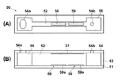
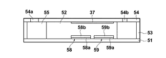
本発明の検出用試料セルは、上述の本発明の検出方法に使用される試料セルであって、
液体試料が流下される流路を有する基台と、
前記流路の上流側に設けられた該流路に前記液体試料を注入するための注入口と、
前記流路の下流側に設けられた、前記注入口から注入された前記液体試料を該下流側に流すための空気孔と、
前記流路の、前記注入口と前記空気孔との間に設けられたセンサチップ部であって、前記流路の内壁面の少なくとも一部として設けられた誘電体プレートと、該プレートの試料接触面に設けられた少なくとも金属層を含むセンサ部とからなるセンサチップ部とを備えてなることを特徴とするものである。
The detection sample cell of the present invention is a sample cell used in the above-described detection method of the present invention,
A base having a channel through which a liquid sample flows;
An inlet for injecting the liquid sample into the channel provided upstream of the channel;
An air hole provided on the downstream side of the flow path for flowing the liquid sample injected from the injection port to the downstream side;
A sensor chip portion provided between the inlet and the air hole of the flow path, the dielectric plate provided as at least a part of the inner wall surface of the flow path, and a sample contact of the plate And a sensor chip part including at least a sensor part including a metal layer provided on the surface.
検出用試料セルにおいては、前記センサ部に、前記蛍光標識結合物質と結合する固定層を備えていることが望ましい。 In the sample cell for detection, it is desirable that the sensor unit includes a fixed layer that binds to the fluorescent label binding substance.
さらに、複数の蛍光色素分子を、該蛍光色素分子からの蛍光を透過する材料により包含してなる、帯電した蛍光物質を、前記蛍光標識として含む前記蛍光標識結合物質が、前記流路内の、前記センサ部より上流側に固定されていることが望ましい。 Further, the fluorescent label-binding substance containing a charged fluorescent substance as the fluorescent label, which includes a plurality of fluorescent dye molecules by a material that transmits fluorescence from the fluorescent dye molecule, It is desirable that the sensor unit is fixed upstream.
本発明の試料セルは、前記固定層が、前記被検出物質と特異的に結合する第1の結合物質が固定されてなる層であり、前記蛍光標識結合物質が、前記被検出物質と特異的に結合する第2の結合物質を含み、前記被検出物質を介して前記第1の結合物質と結合するものであれば、サンドイッチ法によるアッセイを行うのに好適なものとなる。 In the sample cell of the present invention, the immobilization layer is a layer formed by immobilizing a first binding substance that specifically binds to the target substance, and the fluorescent label binding substance is specific to the target substance. A substance that contains a second binding substance that binds to and binds to the first binding substance via the substance to be detected is suitable for performing an assay by the sandwich method.
また、本発明の試料セルは、前記固定層が、前記被検出物質と特異的に結合する第1の結合物質が固定されてなる層であり、前記蛍光標識結合物質は、前記第1の結合物質と特異的に結合する第3の結合物質を含み、前記被検出物質と競合して前記第1の結合物質と結合するものであれば、競合法によるアッセイを行うのに好適なものとなる。 In the sample cell of the present invention, the immobilization layer is a layer formed by immobilizing a first binding substance that specifically binds to the target substance, and the fluorescent label binding substance is the first binding substance. A substance that contains a third binding substance that specifically binds to a substance and that competes with the substance to be detected and binds to the first binding substance is suitable for performing an assay by a competition method. .
さらに、前記センサ部において、前記金属層上に光導波層が備えられていてもよい。 Furthermore, in the sensor unit, an optical waveguide layer may be provided on the metal layer.
本発明の検出用キットは、上述の本発明の検出方法に使用される検出用キットであって、
液体試料が流下される流路を有する基台と、前記流路の上流側に設けられた該流路に前記液体試料を注入するための注入口と、前記流路の下流側に設けられた、前記注入口から注入された前記液体試料を該下流側に流すための空気孔と、前記流路の、前記注入口と前記空気孔との間に設けられたセンサチップ部であって、前記流路の内壁面の少なくとも一部として設けられた誘電体プレートと、該プレートの試料接触面に設けられた少なくとも金属層を含むセンサ部とからなるセンサチップ部と、該センサ部上に固定された、前記蛍光標識結合物質と結合する固定層とを備えた試料セル、および
前記液体試料と同時もしくは前記液体試料の流下後に、前記流路内に流下される、複数の蛍光色素分子を、該蛍光色素分子からの蛍光を透過する材料により包含してなる帯電した蛍光物質を、前記蛍光標識として含む前記蛍光標識結合物質を含んだ標識用溶液を備えてなることを特徴とするものである。
The detection kit of the present invention is a detection kit used in the detection method of the present invention described above,
A base having a channel through which the liquid sample flows, an inlet for injecting the liquid sample into the channel provided on the upstream side of the channel, and provided on the downstream side of the channel An air hole for flowing the liquid sample injected from the injection port to the downstream side, and a sensor chip portion of the flow channel provided between the injection port and the air hole, A sensor chip part comprising a dielectric plate provided as at least a part of the inner wall surface of the flow path, and a sensor part including at least a metal layer provided on the sample contact surface of the plate, and fixed on the sensor part In addition, a sample cell including a fixed layer that binds to the fluorescent label binding substance, and a plurality of fluorescent dye molecules that flow down into the flow path simultaneously with the liquid sample or after the liquid sample flows down, Materials that transmit fluorescence from fluorescent dye molecules It is characterized by comprising a labeling solution containing the fluorescent label-binding substance containing a charged fluorescent substance included as a fluorescent label as the fluorescent label.
さらに、前記試料セルは、前記センサ部において、前記金属層上に光導波層が備えられていでもよい。 Furthermore, the sample cell may include an optical waveguide layer on the metal layer in the sensor unit.
本発明の検出用キットは、前記試料セルの前記固定層が、前記被検出物質と特異的に結合する第1の結合物質が固定されてなる層であり、前記標識用溶液が、前記蛍光標識結合物質として、前記被検出物質と特異的に結合する第2の結合物質を含む、前記被検出物質を介して前記第1の結合物質と結合するものを備えている場合には、サンドイッチ法によるアッセイを行うのに好適なものとなる。また、前記試料セルの前記固定層が、前記被検出物質と特異的に結合する第1の結合物質が固定されてなる層であり、前記標識用溶液が、前記蛍光標識結合物質として、前記第1の結合物質と特異的に結合する第3の結合物質を含む、前記被検出物質と競合して前記第1の結合物質と結合するものを備えている場合には、競合法によるアッセイを行うのに好適なものとなる。 In the detection kit of the present invention, the fixing layer of the sample cell is a layer in which a first binding substance that specifically binds to the substance to be detected is fixed, and the labeling solution is the fluorescent label. When the binding substance includes a second binding substance that specifically binds to the substance to be detected, and a substance that binds to the first binding substance via the substance to be detected, the sandwich method is used. It will be suitable for conducting the assay. The immobilization layer of the sample cell is a layer formed by immobilizing a first binding substance that specifically binds to the substance to be detected, and the labeling solution is used as the fluorescent label binding substance. In the case where a substance that contains a third binding substance that specifically binds to one binding substance and binds to the first binding substance in competition with the substance to be detected is provided, an assay by a competition method is performed. It becomes a suitable thing.
なお、前記金属層の材料としては、Au、Ag、Cu、Al、Pt、Ni、Ti、およびこれらの合金からなる群より選択される少なくとも1種の金属を主成分とすることが望ましい。なおここで、「主成分」は、含量90質量%以上の成分と定義する。 The material of the metal layer is preferably composed mainly of at least one metal selected from the group consisting of Au, Ag, Cu, Al, Pt, Ni, Ti, and alloys thereof. Here, the “main component” is defined as a component having a content of 90% by mass or more.
本発明の検出方法および装置によれば、センサ部上に、試料に含有される被検出物質の量に応じて結合される蛍光標識結合物質の蛍光標識として、複数の蛍光色素分子を、該蛍光色素分子からの蛍光を透過する材料により包含してなる、帯電した蛍光物質を用い、試料に電圧を印加することにより、光電場増強効果の高いセンサ部表面に蛍光物質を引き寄せた状態で、その蛍光標識結合物質の蛍光標識の励起に起因して生じる光の量を検出するので、センサ部表面の増強度の大きい光電場を効率よく利用することができ、かつ蛍光標識の表面からの距離を一様にすることができるため、信号強度のばらつきを抑制することができる。すなわち、S/Nのよい安定した信号を検出することができ、被検出物質の有無および/または量を精度よく検出することができる。 According to the detection method and apparatus of the present invention, a plurality of fluorescent dye molecules are used as a fluorescent label of a fluorescent label binding substance that is bound on the sensor unit according to the amount of the target substance contained in the sample. By using a charged fluorescent substance that is included in the material that transmits the fluorescence from the dye molecule, and applying a voltage to the sample, the fluorescent substance is attracted to the surface of the sensor unit with a high photoelectric field enhancement effect. Since the amount of light generated due to the excitation of the fluorescent label of the fluorescent label binding substance is detected, it is possible to efficiently use a photoelectric field having a large intensity on the surface of the sensor unit and to reduce the distance from the surface of the fluorescent label. Since it can be made uniform, variation in signal intensity can be suppressed. That is, a stable signal with a good S / N can be detected, and the presence and / or amount of the substance to be detected can be accurately detected.
本発明の検出用試料セルあるいは検出用キットを用いれば、本発明の検出方法を容易に実施することができ、増強された光電場を有効に利用し、かつ信号強度のばらつきを抑制し、被検出物質の有無および/または量を精度よく検出することができる。 If the detection sample cell or detection kit of the present invention is used, the detection method of the present invention can be easily carried out, the enhanced photoelectric field can be used effectively, the variation in signal intensity can be suppressed, and the The presence and / or amount of the detection substance can be detected with high accuracy.
以下、図面を参照して本発明の実施形態について説明する。なお、各図において説明の便宜上、各部の寸法は実際のものとは異ならせている。
「検出方法および装置」
本発明の検出方法は、例えば図1に示すように、誘電体プレート11と、該プレート11の一面に設けられた少なくとも金属層12を含むセンサ部14とからなるセンサチップ10を用い、センサ部14に試料を接触させることにより、該センサ部14上に、該試料に含有される被検出物質Aの量に応じた量の蛍光標識結合物質BFを結合させ、センサ部14に励起光L0を照射することにより、センサ部14上に増強した光電場Dを生じさせ、該増強した光電場D内において、蛍光標識結合物質BFの蛍光標識Fの励起し、該蛍光標識の励起に起因して生じる光の量に基づいて、被検出物質Aの量を検出する検出方法であって、蛍光標識として、複数の蛍光色素分子fを、該蛍光色素分子fからの蛍光を透過する材料により包含してなる、帯電した蛍光物質Fを用い、センサ部14に蛍光標識結合物質を結合させた状態で、液体試料に対して電圧を印加することにより、帯電した蛍光物質Fをセンサ部14に引き寄せ、該蛍光物質Fを引き寄せた状態で被検出物質Aの量を検出することを特徴とする。
Hereinafter, embodiments of the present invention will be described with reference to the drawings. For convenience of explanation in each figure, the dimensions of each part are different from the actual ones.
"Detection method and apparatus"
For example, as shown in FIG. 1, the detection method of the present invention uses a
なお、センサ部14に、蛍光標識結合物質を結合させる際に、液体試料に対して、帯電した蛍光物質をセンサ部に引き寄せる第1の電圧を印加し、蛍光標識結合物質を結合させた後、第1の電圧の印加を停止し、該第1の電圧とは逆向きの電場を生じさせる第2の電圧を印加し、液体試料中の、センサ部に結合していない蛍光標識結合物質を該センサ部上から除去し、その後、被検出物質の量を検出することが望ましい。センサ部に蛍光標識結合物質を結合させる際に、センサ部に蛍光標識結合物質を引き寄せることにより、センサ部における蛍光標識結合物質の濃度を高めてセンサ部への結合を促進させることができ、その後第2の電圧を印加することにより、センサ部に結合せず、滞留あるいは非特異吸着している蛍光標識結合物質を電荷反発により効率的に取り除くことができる。なお、ここで、センサ部に結合するとは、センサ部に対して特異的に結合することを意味し、具体的には、蛍光標識結合物質が特異的に結合する物質が固定層としてセンサ部に設けられており、この固定層に結合する形態が挙げられる。
In addition, when binding the fluorescent label binding substance to the
本発明の検出装置は、上記検出方法を実施するためのものであって、センサチップ10を収容する収容部19と、センサ部14に励起光L0を照射する励起光照射光学系20と、励起光L0の照射により生じる、被検出物質Aに応じた量の光を検出する光検出手段30と、収容部19にセンサチップ10が収容された際に、液体試料に対して電圧印加する電圧印加手段35とを備えている。
Detection device of the present invention is for implementing the above detection method, an
蛍光標識は、図1の一部に拡大して示すように、複数の蛍光色素分子fを、該複数の蛍光色素分子fから生じる蛍光を透過する材料16により包含してなる蛍光物質を用いることが好ましい。複数の蛍光色素分子fを含む蛍光物質Fを用いれば、蛍光量を増加させることができるからである。また、蛍光Lfを透過する材料16により蛍光色素分子fが内包されていることにより、金属層と所定以上の距離を保つことができ、蛍光色素分子fが金属層12に近接した場合に生じる金属消光を防止することができる。
As shown in an enlarged view of a part of FIG. 1, the fluorescent label uses a fluorescent substance that includes a plurality of fluorescent dye molecules f by a
蛍光色素分子が金属層に接近しすぎた場合に生じる消光は、金属へのエネルギー移動に伴うものであり、このエネルギー移動の程度は、金属が半無限の厚さを持つ平面なら距離の3乗に反比例して、金属が無限に薄い平板なら距離の4乗に反比例して、また、金属が微粒子なら距離の6乗に反比例して小さくなる。従って、金属層12と蛍光色素分子fとの間の距離は少なくとも数nm以上、より好ましくは10nm以上確保しておくことが望ましい。
従来金属消光を防止する方法としては、金属層12上に自己組織化膜(SAM)を形成し、さらにカルボキシメチルデキストラン(CMD)膜を作製して金属膜と蛍光色素分子との距離を離す方法が知られている。しかしながら、金属膜上にこれらの金属消光を防止するための膜を設けるのは、センサチップ作製工程を複雑なものとし、非常に手間がかかる。一方、蛍光物質Fを用いれば、上述のような金属消光防止のための膜を設けることなく、非常に簡便な方法で効果的に金属消光を防止することができる。
The quenching that occurs when the fluorescent dye molecules are too close to the metal layer is associated with the energy transfer to the metal, and the degree of this energy transfer is the cube of the distance if the metal is a plane with a semi-infinite thickness. When the metal is an infinitely thin flat plate, it is inversely proportional to the fourth power of the distance, and when the metal is a fine particle, it is decreased inversely proportional to the sixth power of the distance. Therefore, it is desirable to ensure the distance between the
Conventionally, as a method for preventing metal quenching, a self-assembled film (SAM) is formed on the
材料16としては、具体的には、ポリスチレンやSiO2などが挙げられるが、蛍光色素分子fを内包でき、かつ、該蛍光色素分子fからの蛍光を透過させて外部に放出できるものであれば特に制限されない。 Specific examples of the material 16 include polystyrene, SiO 2 , and the like, as long as they can encapsulate the fluorescent dye molecule f and can transmit the fluorescence from the fluorescent dye molecule f to be emitted to the outside. There is no particular limitation.
なお、蛍光物質は、試料に対して電圧が印加された場合に、液体試料中においてブラウン運動よりも電極への引き寄せ効果が大きくなる程度の電荷が帯電されていることが望ましい。被検出物質となりうるタンパク、生体分子のうちでサイズが大きいものとしては、抗体(〜15nm)、アルブミン(〜20nm)などがあるが、被検出物質を帯電させるだけでは不十分である。従って、蛍光物質としては、粒径が30nm程度以上の大きさあることが好ましい。粒径が30nm未満であると、物質のブラウン運動により、十分な引き寄せ効果が得られない場合が生じる恐れがある。なお、蛍光物質の粒径が70nm以上、さらには、100nm以上であれば、より効果的な引き寄せが期待できる。 In addition, it is desirable that the fluorescent material is charged with an electric charge in such a degree that when the voltage is applied to the sample, the attracting effect to the electrode is greater than the Brownian motion in the liquid sample. Among proteins and biomolecules that can be detected substances, there are antibodies (˜15 nm), albumin (˜20 nm), etc., but it is not sufficient to charge the detected substance. Accordingly, the fluorescent material preferably has a particle size of about 30 nm or more. If the particle size is less than 30 nm, there may be a case where a sufficient pulling effect cannot be obtained due to the Brownian motion of the substance. In addition, if the particle size of the fluorescent material is 70 nm or more, and further 100 nm or more, more effective attraction can be expected.
また、拡散時間の点から粒径が5300nm以下のものが好ましい。また、蛍光量およびセンサ部上への最密充填密度の観点および、表面プラズモンの擾乱の観点から70nm〜900nmのものがさらに好ましく、130nm〜500nmのものが特に好ましい。 Moreover, the thing of a particle size of 5300 nm or less is preferable from the point of the diffusion time. Further, from the viewpoint of the amount of fluorescence and the closest packing density on the sensor part and from the viewpoint of disturbance of the surface plasmon, those of 70 nm to 900 nm are more preferable, and those of 130 nm to 500 nm are particularly preferable.
蛍光物質Fは、例えば、以下のようにして作製することができる。
まず、ポリスチレン粒子(Estapor社、φ500nm、10%solid、カルボキシル基、製品番号K1―050)を調液して0.1%solid in phosphate(ポリスチレン溶液:pH7.0)を作製する。
次に、蛍光色素分子(林原生物化学研究所 NK−2014(励起 〜780nm))0.3mgの酢酸エチル溶液(1mL)を作製する。
上記ポリスチレン溶液と蛍光色素溶液を混合し、エバポレートしながら含浸を行った後、遠心分離(15000rpm、4℃、20分を2回)を行い、上清を除去する。以上の工程により、ポリスチレンにより蛍光色素を内包してなる蛍光物質Fを得ることができる。このような手順で、ポリスチレン粒子に蛍光色素を含浸させて作製された蛍光物質Fの粒径はポリスチレン粒子の粒径と同一(上記例ではφ500nm)となる。なお、上記において用いるポリスチレン粒子は表面にpHに応じて荷電状態が変化する官能基であるカルボキシル基が修飾されていることから、蛍光物質Fは表面にカルボキシル基が修飾されたものとなっており、液体試料中において、カルボキシル基がイオン化することにより、負に帯電される。
The fluorescent substance F can be produced as follows, for example.
First, polystyrene particles (Estapoor, φ500 nm, 10% solid, carboxyl group, product number K1-050) are prepared to prepare 0.1% solid inphosphate (polystyrene solution: pH 7.0).
Next, a 0.3 mg ethyl acetate solution (1 mL) of fluorescent dye molecules (Hayashibara Biochemical Research Institute NK-2014 (excitation-780 nm)) is prepared.
The polystyrene solution and the fluorescent dye solution are mixed and impregnated while evaporating, and then centrifuged (15000 rpm, 4 ° C., 20 minutes twice) to remove the supernatant. Through the above steps, a fluorescent substance F formed by encapsulating a fluorescent dye with polystyrene can be obtained. In such a procedure, the particle size of the fluorescent substance F produced by impregnating the polystyrene particles with the fluorescent dye is the same as the particle size of the polystyrene particles (φ500 nm in the above example). In addition, since the polystyrene particle used in the above is modified with a carboxyl group which is a functional group whose charge state changes depending on pH on the surface, the fluorescent substance F has a carboxyl group modified on the surface. In the liquid sample, the carboxyl group is negatively charged by ionization.
蛍光標識結合物質BFは、被検出物質Aの量に応じた量だけセンサ部14上に結合する蛍光標識された結合物質であり、図1で示すように、サンドイッチ法によるアッセイを行う場合には、被検出物質と特異的に結合する結合物質と上述の蛍光物質Fとから構成されるものであり、後記する競合法によるアッセイを行う場合には、被検出物質と競合する結合物質と蛍光物質Fとから構成されるものである。より具体的には、センサチップ10として、センサ部14に被検出物質Aと特異的に結合する第1の結合物質B1が固定層として固定されたものを用いた場合、サンドイッチ法では、蛍光標識結合物質BFとして、被検出物質Aと特異的に結合する第2の結合物質B2と、この結合物質B2が修飾された蛍光物質Fとからなるものを用い、競合法では、蛍光標識結合物質として、被検出物質Aと競合して第1の結合物質と特異的に結合する第3の結合物質と、この結合物質が修飾された蛍光物質Fとからなるものを用いる。被検出物質Aが抗原である場合、第1の結合物質B1として所謂1次抗体を用い、蛍光標識結合物質として所謂標識2次抗体を用いればよい。
The fluorescently labeled binding substance BF is a fluorescently labeled binding substance that binds on the
蛍光物質Fを帯電させる方法としては、蛍光物質Fの表面に少なくとも液体試料中で極性を有する官能基を修飾しておく方法が好ましい。液体試料中においてイオン化し正電荷もしくは負電荷を有する官能基としては、カルボキシル基、スルホン酸基、リン酸基、アミノ基、4級アンモニウム基、イミダゾール基、及びグアニジニウム基などを用いることができる。例えば、カルボキシル基(−COOH)は、血清、血漿などの液体試料中、もしくはリン酸緩衝生理食塩水(Phosphate buffered saline, PBS)中などにおいて、COO−にイオン化した状態となり、蛍光物質Fを負に帯電させることができる。また、アミノ基(−NH2)は、血清、血漿などの液体試料中、もしくはPBS中などにおいて、NH3 +にイオン化した状態となり、蛍光物質Fを正に帯電させることができる。 As a method for charging the fluorescent substance F, a method in which the surface of the fluorescent substance F is modified with a functional group having polarity in at least a liquid sample is preferable. As the functional group ionized in the liquid sample and having a positive charge or a negative charge, a carboxyl group, a sulfonic acid group, a phosphoric acid group, an amino group, a quaternary ammonium group, an imidazole group, a guanidinium group, or the like can be used. For example, a carboxyl group (—COOH) is ionized into COO − in a liquid sample such as serum or plasma, or in phosphate buffered saline (PBS), and the fluorescent substance F is negatively charged. Can be charged. In addition, the amino group (—NH 2 ) is ionized into NH 3 + in a liquid sample such as serum or plasma, or in PBS, and the fluorescent substance F can be positively charged.
蛍光物質が負に帯電している場合、金属膜側を正極として電圧を印加することにより、蛍光物質を金属膜に引き寄せることができ、蛍光物質が正に帯電している場合、金属膜側を負極として電圧を印加することにより、蛍光物質を金属膜に引き寄せることができる。 When the fluorescent material is negatively charged, the fluorescent material can be attracted to the metal film by applying a voltage with the metal film side as the positive electrode. When the fluorescent material is positively charged, the metal film side is By applying a voltage as the negative electrode, the fluorescent material can be attracted to the metal film.
既述の図17の例では、蛍光標識が十分に金属層上に引き寄せられず、また、結合体の直立、横臥により蛍光標識のセンサ面からの距離にばらつきが生じていたが、蛍光標識として用いる蛍光物質を帯電させることにより、該蛍光物質を効率的に、かつ一様にセンサ部表面に引き寄せることができる。これにより、S/Nよく安定した信号を検出することが可能となる。 In the example of FIG. 17 described above, the fluorescent label is not sufficiently attracted on the metal layer, and the distance from the sensor surface of the fluorescent label varies due to the upright or lying of the conjugate. By charging the fluorescent substance to be used, the fluorescent substance can be attracted to the sensor portion surface efficiently and uniformly. As a result, it is possible to detect a stable signal with good S / N.
本発明は、励起光の照射によりセンサ部上に増強した光電場を生じさせ、その増強した光電場において蛍光標識が励起されることによって生じる光を検出するものであるが、光電場を増強させる方法は、表面プラズモン共鳴あるいは局在プラズモン共鳴によるものであってもよいし、光導波モードの励起によるものであってもよい。また、蛍光標識から生じる蛍光を直接検出してもよいし、間接的に検出してもよい。具体的な態様については、以下の各実施形態で説明する。 In the present invention, an enhanced photoelectric field is generated on a sensor unit by irradiation of excitation light, and light generated by excitation of a fluorescent label in the enhanced photoelectric field is detected. The method may be based on surface plasmon resonance or localized plasmon resonance, or may be based on excitation of an optical waveguide mode. Further, the fluorescence generated from the fluorescent label may be detected directly or indirectly. Specific embodiments will be described in the following embodiments.
<第1の実施形態>
第1実施形態の検出方法および装置について図1を参照して説明する。図1は第1の実施形態の検出装置の概略構成を示す全体図である。本実施形態の検出方法および装置は、表面プラズモン共鳴により光電場を増強させ、増強された光電場において励起された蛍光を検出する蛍光検出方法および装置である。
<First Embodiment>
A detection method and apparatus according to the first embodiment will be described with reference to FIG. FIG. 1 is an overall view showing a schematic configuration of a detection apparatus according to the first embodiment. The detection method and apparatus of the present embodiment is a fluorescence detection method and apparatus that enhances a photoelectric field by surface plasmon resonance and detects fluorescence excited in the enhanced photoelectric field.
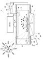
本実施形態の本蛍光検出方法では、誘電体プレート11およびその一面の所定領域に少なくとも金属層12として金属膜が設けられてなるセンサ部14を備えたセンサチップ10を用い、このセンサチップ10上に液体試料Sを保持する試料保持部13が備えられ、センサチップ10と液体試料を保持可能な試料保持部13による箱状の試料セルを用いている。なお、試料保持部13の上板には、金属層12との間に充填される液体試料に電圧を印加するための対向電極36が設けられている。
金属膜12は、所定領域に開口を有するマスクをプレート11の一表面に形成し、既知の蒸着法で成膜形成することができる。金属膜12の厚みは、金属膜12の材料と、励起光の波長により表面プラズモンが強く励起されるように適宜定めることが望ましい。例えば、励起光として780nmに中心波長を有するレーザ光を用い、金属膜として金(Au)膜を用いる場合、金属膜の厚みは50nm±20nmが好適である。さらに好ましくは、47nm±10nmである。なお、金属膜は、Au、Ag、Cu、Al、Pt、Ni、Ti、およびこれらの合金からなる群より選択される少なくとも1種の金属を主成分とするものが好ましい。
In the present fluorescence detection method of the present embodiment, a
The
本蛍光検出装置1は、センサチップ10を収容する収容部19と、収容部19に収容されたセンサチップ10の誘電体プレート11と金属膜12との界面に励起光Loを全反射角以上の入射角度で、センサチップ10の金属膜形成面とは反対の他面側から入射させる励起光照射光学系20と、励起光の照射により生じる蛍光Lfを検出する光検出器30とを備えている。またさらに、該収容部19にセンサチップが収容された際に液体試料に対して電圧を印加するための電圧印加手段35を備えている。
The fluorescence detection device 1 is configured to receive excitation light Lo at a total reflection angle or more at the interface between the
励起光照射光学系20は、励起光Loを出力する半導体レーザ(LD)等からなる光源21と、誘電体プレート11に一面が接触するように配置されたプリズム22とを備えている。プリズム22は、誘電体プレート11と金属膜12との界面で励起光Loが全反射するように誘電体プレート11内に励起光Loを導光するものである。なお、プリズム22と誘電体プレート11とは、屈折率マッチングオイルを介して接触されている。光源21は、プリズム22の他の一面からセンサチップ10の試料接触面10aで励起光Loが全反射角以上で、かつ金属膜で表面プラズモン共鳴する特定の角度で入射するように配置されている。さらに、光源21とプリズム22との間に必要に応じて導光部材を配置してもよい。なお、励起光Loは、表面プラズモンを誘起するようにp偏光で界面に対して入射させる。
The excitation light irradiation
光検出器30としては、CCD、PD(フォトダイオード)、フォトマルチプライア、c−MOS等を適宜用いることができる。
As the
収容部19は、センサチップ10を収容する際に、センサチップのセンサ部14がプリズム22上に配置され、光検出器30で蛍光が検出できるよう構成されている。収容部19に対しセル(センサチップ10)を、図中矢印X方向に出し入れすることができる。
The
電圧印加手段35は、直流電源31と、電圧のオン/オフを行うためのスイッチ32から構成されている。本実施形態においては、金属膜を正極として第1の電圧を印加するための第1の電源31aと、金属膜を負極として第2の電圧を印加するための第2の電源31bとが備えられており、スイッチ32により適宜切り替え可能とされており、誘電体プレート11上に設けられた金属膜12を電極として用い、該金属膜12とセルの上板に設けられた対向電極36との間に電圧を印加するよう構成されている。なお、セルの上板に設けられた対向電極36は、透明電極で構成されている。なお、対向電極36としては、蛍光を検出するための開口を有する形状の金属電極を設けてもよい。
The voltage application means 35 includes a DC power supply 31 and a
なお、ここでは、金属層を電極として用いる構成について説明したが、金属層とは別にセンサ部近傍に電極を設けてもよい。金属層を電極として用いない場合は、測定部の近傍に蒸着もしくはメッキにより金属電極を設ければよい。さらに、プレート11を、ポリアニリン、ポリピロールのような透明かつ導電性の高い樹脂にて作製することもできる。この場合、ポリアニリン等を単独で成形することも可能であるし、ポリスチレンのような別樹脂に混ぜて導電性を持たせることも可能である。また、試料保持部の上板に対向電極が設けられている構成に限らず、液体試料中に抜き差し可能な導電体を対向電極として用いてもよい。
In addition, although the structure which uses a metal layer as an electrode was demonstrated here, you may provide an electrode in the sensor part vicinity separately from a metal layer. When a metal layer is not used as an electrode, a metal electrode may be provided near the measurement unit by vapor deposition or plating. Further, the
蛍光検出装置1を用いた本実施形態の蛍光検出方法について説明する。
ここでは、一例として、試料Sに含まれる被測定物質として抗原Aを検出する場合について説明する。
The fluorescence detection method of the present embodiment using the fluorescence detection device 1 will be described.
Here, as an example, a case where the antigen A is detected as the substance to be measured contained in the sample S will be described.
センサチップ10として、センサチップ10の金属膜12上に、抗原Aと特異的に結合する第1の結合物質として1次抗体B1が固定層として修飾されているものを用意する。
まず、試料保持部13中に検査対象である液体試料Sを流し、センサチップ10の金属膜12上に試料Sを接触させる。次いで同様に抗原Aと特異的に結合する第2の結合物質である2次抗体B2と蛍光標識Fとからなる蛍光標識結合物質(標識2次抗体)BFを含む溶液を流す。この場合、金属膜12に表面修飾される1次抗体B1と蛍光標識結合物質BFの2次抗体B2として、被検出物質である抗原Aに対して互いに別の部位に結合するものを用いる。なお、ここでは、蛍光標識として、蛍光色素分子fを内包する、カルボキシル基(−COOH)が表面に修飾されてなる蛍光物質Fを用いている。カルボキシル基は液体試料中においてCOO−にイオン化し、蛍光物質Fは負に帯電したものとなる。
A
First, the liquid sample S to be inspected is caused to flow through the
試料S中に抗原Aが存在すれば、1次抗体B1に抗原Aが特異的に結合し、さらに抗原Aに蛍光標識結合物質BFの2次抗体B2が結合して、1次抗体B1−抗原A−2次抗体B2結合体(以下、サンドイッチ結合体という。)が形成される。このとき、電圧印加手段35のスイッチ32を第1の電源31aに接続して金属膜12側を正極として電極間に第1の電圧を印加しておくことにより、負に帯電した蛍光物質Fを含む蛍光標識結合物質BFが金属膜12に引き寄せられ、金属膜上における蛍光標識結合物質の濃度を高めることができ、抗原―抗体反応を促進し、反応時間を短縮させることができる。
If antigen A is present in sample S, antigen A specifically binds to primary antibody B 1 , and further, secondary antibody B 2 of fluorescently labeled binding substance BF binds to antigen A, and primary antibody A B 1 -antigen A-2 secondary antibody B 2 conjugate (hereinafter referred to as a sandwich conjugate) is formed. At this time, the
その後、サンドイッチ結合体と、未反応の蛍光標識結合物質BFを分離するため、緩衝液を流し、未反応の蛍光標識結合物質を排除する。このとき、電圧印加手段35のスイッチ32を切り替えて第2の電源31bに接続して金属膜12側を負極として第2の電圧を印加しておくことにより、負に帯電した蛍光物質Fに電荷反発が働き、未反応の蛍光標識蛍光物質を効率よく排除することができる。
Thereafter, in order to separate the sandwich conjugate from the unreacted fluorescently labeled binding substance BF , a buffer is passed to eliminate the unreacted fluorescently labeled binding substance. At this time, the
被検出物質(抗原A)への標識のタイミングは特に制限されず、被検出物質(抗原A)を第1の結合物質(1次抗体B1)に結合させる前に、予め試料に蛍光標識を添加しておいてもよい。 The timing of labeling the substance to be detected (antigen A) is not particularly limited. Before the substance to be detected (antigen A) is bound to the first binding substance (primary antibody B 1 ), the sample is previously labeled with a fluorescent label. It may be added.
その後、センサチップ10を収容部19にセットした状態で、電圧印加手段35のスイッチを第1の電源に接続して金属膜12側を正極として電極間に電圧を印加することにより、センサ部上に結合している蛍光標識結合物質BFの、負に帯電した蛍光物質Fをセンサ部14に引き寄せる。このように、蛍光物質Fをセンサ部14に引き寄せた状態で、センサチップ10の誘電体プレート11の所定領域に向けて励起光照射光学系20により励起光Loを照射する。励起光照射光学系20により励起光Loが誘電体プレート11と金属膜12との界面に対して全反射角以上の特定の入射角度で入射されることにより、金属膜上12の試料S中にエバネッセント波が滲み出し、このエバネッセント波によって金属膜12中に表面プラズモンが励起される。励起光の入射により金属層上に生じている光電場(エバネッセント波に起因する電場)が、この表面プラズモンにより増強され、金属層上に光電場増強領域Dが形成される。電場増強領域の金属膜表面には、電圧印加手段35による電圧印加により、帯電した蛍光物質Fが引き寄せられており、蛍光物質Fが励起されて(実質的にはその蛍光物質中の蛍光色素分子fが励起されて)蛍光Lfが発生する。表面プラズモンによる光電場増強の効果により蛍光は増強されたものとなる。光検出器30によりこの蛍光Lfを検出することにより、蛍光標識結合物質と結合した被検出物質の有無および/または量を検出することができる。
Thereafter, in a state where the
また、センサ部上にサンドイッチ結合物を形成させ、サンドイッチ結合物と、未反応の蛍光標識結合物質BFとを分離する工程は、必ずしも電圧を印加して行う必要はなく、電圧を印加して行わない場合には、この工程は、センサチップ10を検出装置1の収容部19にセットする前に行ってもよいし、セット後に行ってもよい。またこの場合、電圧印加手段には、直流電源として、金属膜を負極として電圧を印加するための電源のみを備えればよい。
In addition, the step of forming a sandwich bond on the sensor unit and separating the sandwich bond from the unreacted fluorescent label binding substance BF is not necessarily performed by applying a voltage. When not performing, this process may be performed before setting the
このように、電極間に電圧を印加して試料中に電場を生じさせて、帯電した蛍光物質をセンサ部に引き寄せた状態で蛍光を検出することにより、安定したS/Nよい信号を得ることができ、検査の信頼性を向上させることができる。 Thus, a stable signal with a good S / N can be obtained by applying a voltage between the electrodes to generate an electric field in the sample and detecting the fluorescence while the charged fluorescent substance is attracted to the sensor unit. It is possible to improve the reliability of inspection.
<第1の実施形態の設計変更例>
上述の各実施形態においては励起光Loとして、界面に所定の角度θで入射する平行光を入射するものとしたが、励起光としては、図2に模式的に示すような、角度θを中心に角度幅Δθを持つファンビーム(集束光)を用いてもよい。ファンビームの場合、プリズム122とプリズム上の金属膜112との界面に対して、角度θ―Δθ/2〜θ+Δθ/2の範囲の入射角度で入射することになり、この角度範囲内に共鳴角があれば、金属膜112に表面プラズモンを励起することができる。金属膜上への試料供給の前後において、金属膜上の媒質の屈折率が変化し、そのために表面プラズモンが生じる共鳴角が変化する。上述の実施形態のように平行光を励起光として用いる場合、共鳴角が変化するたびに平行光の入射角度を調整する必要がある。しかし、図2に示すような、界面に入射する入射角度に幅を持たせたファンビームを用いることにより、入射角度の調整をすることなく、共鳴角の変化に対応することができる。なお、ファンビームは入射角度による強度変化が少ないフラットな分布を持つものであることがより好ましい。
<Design change example of the first embodiment>
In each of the embodiments described above, parallel light incident on the interface at a predetermined angle θ is incident as the excitation light Lo, but the excitation light is centered on the angle θ as schematically shown in FIG. Alternatively, a fan beam (focused light) having an angular width Δθ may be used. In the case of a fan beam, the light beam is incident on the interface between the
<第2の実施形態>
第2の実施形態である検出方法および装置について図3を参照して説明する。図3は第2の実施形態の検出装置の概略構成を示す全体図である。本実施形態の検出方法および装置は、局在プラズモン共鳴により光電場を増強させ、増強された光電場において励起された蛍光を検出する蛍光検出方法および装置である。なお、以下においては、第1実施形態と同じ構成要素には同じ参照符号を付してある。
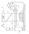
<Second Embodiment>
A detection method and apparatus according to the second embodiment will be described with reference to FIG. FIG. 3 is an overall view showing a schematic configuration of the detection apparatus according to the second embodiment. The detection method and apparatus of the present embodiment is a fluorescence detection method and apparatus that enhances a photoelectric field by localized plasmon resonance and detects fluorescence excited in the enhanced photoelectric field. In the following, the same components as those in the first embodiment are denoted by the same reference numerals.
図3に示す蛍光検出装置2は、用いられるセンサチップ10’と、励起光照射光学系20’とが上述の第1の実施形態の蛍光検出装置1とは異なる。
The
センサチップ10’は誘電体プレート11上に設けられる金属層12’として、励起光の照射を受けて、所謂局在プラズモンを生じる、表面に励起光Loの波長よりも小さい凹凸構造を有する金属微細構造体、あるいは、励起光の波長よりも小さいサイズの複数の金属ナノロッドを備えている。このような局在プラズモンを生じさせる金属層12’を備えた場合には、励起光を金属層12’と誘電体プレート11との界面に全反射するように入射させる必要はなく、ここでは、励起光照射光学系20’は、誘電体プレート上方から励起光Loを照射するよう構成されている。
The
励起光照射光学系20’は、励起光Loを出力する半導体レーザ(LD)等からなる光源21と、励起光Loを反射してセンサチップ10’へ導光するハーフミラー23とを備えている。ハーフミラー23は、励起光Loを反射し、蛍光Lfを透過するものである。
The excitation light irradiation
センサチップ10’の具体例を図4(A)〜(C)に斜視図で示し説明する。
図4(A)に示すセンサチップ10Aは、誘電体プレート11と、該プレート11の所定領域上にアレイ状に固着された複数の金属粒子73aからなる金属微細構造体73で構成されている。金属粒子73aの配列パターンは適宜設計できるが、略規則的であることが好ましい。かかる構成では、金属粒子73aの平均的な径及びピッチが励起光Loの波長よりも小さく設計される。
A specific example of the
A
図4(B)に示すセンサチップ10Bは、誘電体プレート11と、該プレートの上の所定領域に設けられた、金属細線74aが格子状にパターン形成された金属パターン層からなる金属微細構造体74で構成されている。金属パターン層のパターンは適宜設計でき、略規則的であることが好ましい。かかる構成では、金属細線74aの平均的な線幅及びピッチが励起光Loの波長よりも小さく設計される。
A
図4(C)に示すセンサチップ10Cは特開2007−171003号公報に記載のような、Alなどの金属76の陽極酸化の過程で形成される金属酸化物体77の複数の微細孔77a内に成長させた複数のマッシュルーム状の金属75aからなる金属微細構造体75により構成されている。ここでは金属酸化物体77が誘電体プレートに相当する。この金属微細構造体75は、金属体(Al等)の一部を陽極酸化して金属酸化物体(Al2O3等)とし、陽極酸化の過程で形成される金属酸化物体77の複数の微細孔77a内に各々金属75aをメッキ等により成長させて得ることができる。
図4(C)に示す例では、マッシュルーム状の金属75aの頭部が粒子状であり、サンプルプレート表面から見れば、金属微粒子が配列されたような構造になっている。かかる構成では、マッシュルーム状の金属75aの頭部が凸部であり、その平均的な径およびピッチが測定光Lの波長よりも小さく設計される。
A
In the example shown in FIG. 4C, the head of a mushroom-
なお、励起光の照射を受けて局在プラズモンを生じる金属層12’としては、その他、特開2006−322067号公報、特開2006-250924号公報などに記載の金属体を陽極酸化して得られる微細構造体を利用した種々の形態の金属微細構造体を用いることができる。
The
さらには、局在プラズモンを生じさせる金属層は、表面が粗面化された金属膜により構成されていてもよい。粗面化方法としては、酸化還元等を利用した電気化学的な方法等が挙げられる。また、金属層を、サンプルプレート上に配置された複数の金属ナノロッドにより構成してもよい。金属ナノロッドのサイズは、短軸長さが3nm〜50nm程度、長軸長さが25nm〜1000nm程度であり、長軸長さを励起光の波長よりも小さいサイズとする。金属ナノロッドについては、例えば特開2007-139612号公報に記載されている。 Furthermore, the metal layer that generates localized plasmons may be formed of a metal film having a roughened surface. Examples of the roughening method include an electrochemical method using oxidation reduction and the like. Moreover, you may comprise a metal layer by the some metal nanorod arrange | positioned on the sample plate. The metal nanorods have a minor axis length of about 3 nm to 50 nm and a major axis length of about 25 nm to 1000 nm, and the major axis length is smaller than the wavelength of the excitation light. The metal nanorod is described in, for example, Japanese Patent Application Laid-Open No. 2007-139612.
なお、金属層12’として用いられる、金属微細構造体あるいは金属ナノロッドとしては、Au、Ag、Cu、Al、Pt、Ni、Ti、およびこれらの合金からなる群より選択される少なくとも1種の金属を主成分とするものが好ましい。
The metal microstructure or metal nanorod used as the
蛍光検出装置2を用いた本実施形態の蛍光検出方法について説明する。
センサチップを用意し、抗原―抗体反応をさせる工程は、第1の実施形態と同様であるため、説明を省略する。以下の実施形態において同様とする。
センサチップ10’を収容部19にセットした状態で、電圧印加手段35のスイッチを第1の電源に接続して金属膜12側を正極として電極間に電圧を印加することにより、センサ部上に結合している蛍光標識結合物質BFの、負に帯電した蛍光物質Fをセンサ部14に引き寄せる。このように、蛍光物質Fをセンサ部14に引き寄せた状態で、センサチップ10の誘電体プレート11の所定領域に向けて励起光照射光学系20’により励起光Loを照射する。光源21から出射された励起光Loはハーフミラー23により反射されてセンサチップ10’の試料接触面上に入射される。この励起光Loの照射により、金属層12’の表面で局在プラズモンが励起される。励起光の入射により金属層上に生じている光電場(近接場光に起因する電場)が、この局在プラズモンにより増強され、金属層上に光電場増強領域Dが形成される。光電場増強領域の金属膜表面には、電圧印加手段35による電圧印加により、帯電した蛍光物質Fが引き寄せられており、蛍光物質Fが励起されて(実質的にはその蛍光物質中の蛍光色素分子fが励起されて)蛍光Lfが発生する。局在プラズモンによる光電場増強の効果により蛍光は増強されたものとなる。この蛍光Lfを光検出器30により検出することにより、蛍光標識結合物質と結合した被検出物質の有無および/または量を検出することができる。
The fluorescence detection method of this embodiment using the
The process of preparing the sensor chip and causing the antigen-antibody reaction is the same as in the first embodiment, and thus the description thereof is omitted. The same applies to the following embodiments.
With the
本実施形態においても、蛍光標識結合物質が、帯電した蛍光物質を含み、蛍光物質をセンサ部に引き寄せた状態で蛍光を検出するので、第1の実施形態と同様の効果を得ることができる。 Also in this embodiment, since the fluorescent label binding substance includes a charged fluorescent substance and the fluorescence is detected in a state where the fluorescent substance is attracted to the sensor unit, the same effect as in the first embodiment can be obtained.
<第3の実施形態>
第3の実施形態の検出方法および装置について図5を参照して説明する。図5は第3の実施形態の検出装置の概略構成を示す全体図である。本実施形態の検出方法および装置は、表面プラズモン共鳴により電場を増強させ、増強された電場において励起された蛍光が金属層に新たにプラズモンを誘起することにより、誘電体プレートの金属層形成面と反対の面側から放射される、新たに誘起されたプラズモンからの放射光を検出する放射光検出方法および装置である。
<Third Embodiment>
A detection method and apparatus according to the third embodiment will be described with reference to FIG. FIG. 5 is an overall view showing a schematic configuration of the detection apparatus according to the third embodiment. The detection method and apparatus of the present embodiment enhances an electric field by surface plasmon resonance, and fluorescence excited in the enhanced electric field newly induces plasmon in the metal layer, thereby forming a metal layer forming surface of the dielectric plate. A radiation detection method and apparatus for detecting radiation emitted from a newly induced plasmon emitted from the opposite surface side.
図5に示す放射光検出装置3は、第1の実施形態の蛍光検出装置と光検出器の配置が異なる。本放射光検出装置3においては、光検出器30が、蛍光が金属層に新たに表面プラズモンを誘起することによって誘電体プレートの金属層形成面と反対の面側から放射される、新たに誘起されたプラズモンからの放射光Lpを検出するように配置されている。
The emitted light detection device 3 shown in FIG. 5 differs from the fluorescence detection device of the first embodiment in the arrangement of the photodetectors. In the present radiation light detection device 3, the
放射光検出装置3を用いた本実施形態の放射光検出方法について説明する。
センサチップ10を収容部19にセットした状態で、電圧印加手段35のスイッチを第1の電源に接続して金属膜12側を正極として電極間に電圧を印加することにより、センサ部上に結合している蛍光標識結合物質BFの、負に帯電した蛍光物質Fをセンサ部14に引き寄せる。このように、蛍光物質Fをセンサ部14に引き寄せた状態で、第1の実施形態と同様に、励起光照射光学系20により励起光Loを照射する。励起光照射光学系20により励起光Loが誘電体プレート11と金属膜12との界面に対して全反射角以上の特定の入射角度で入射されることにより、金属膜上12の試料S中にエバネッセント波が滲み出し、このエバネッセント波によって金属膜12中に表面プラズモンが励起される。励起光の入射により金属層上に生じている光電場(エバネッセント波に起因する電場)が、この表面プラズモンにより増強され、金属層上に光電場増強領域Dが形成される。光電場増強領域の金属膜表面には、電圧印加手段35による電圧印加により、帯電した蛍光物質Fが引き寄せられており、蛍光物質Fが励起されて(実質的にはその蛍光物質中の蛍光色素分子fが励起されて)蛍光Lfが発生する。このとき、表面プラズモンによる光電場増強の効果により蛍光は増強されたものとなる。金属膜12上で生じたこの蛍光Lfが、金属膜12に表面プラズモンを新たに誘起し、この表面プラズモンによりセンサチップ10の金属膜形成面と反対側から特定の角度で放射光Lpが射出される。光検出器30によって、この放射光Lpを検出することにより、蛍光標識結合物質と結合した被検出物質の有無および/または量を検出することができる。
A radiation light detection method of the present embodiment using the radiation light detection device 3 will be described.
In a state where the
放射光Lpは蛍光が金属膜の特定の波数の表面プラズモンと結合する際に生じるものであり、蛍光の波長に応じてその結合する波数は定まり、その波数に応じて放射光の出射角度が定まる。通常励起光Loの波長と蛍光の波長とは異なることから、蛍光により励起される表面プラズモンは、励起光Loにより生じた表面プラズモンとは異なる波数のものとなり、励起光Loの入射角度とは異なる角度で放射光Lpは放射される。 The emitted light Lp is generated when the fluorescence is combined with surface plasmons having a specific wave number of the metal film. The wave number to be combined is determined according to the wavelength of the fluorescence, and the emission angle of the emitted light is determined according to the wave number. . Since the wavelength of the excitation light Lo is usually different from the wavelength of the fluorescence, the surface plasmon excited by the fluorescence has a wave number different from that of the surface plasmon generated by the excitation light Lo, and is different from the incident angle of the excitation light Lo. The emitted light Lp is emitted at an angle.
本実施形態においても、蛍光標識結合物質が、帯電した蛍光物質を含み、蛍光物質をセンサ部に引き寄せた状態で蛍光を生じさせ、この増強された蛍光に起因する放射光を検出するので、第1の実施形態と同様の効果を得ることができる。 Also in the present embodiment, the fluorescent label binding substance includes a charged fluorescent substance, generates fluorescence in a state where the fluorescent substance is attracted to the sensor unit, and detects emitted light resulting from the enhanced fluorescence. The same effect as that of the first embodiment can be obtained.
さらに、本実施形態では、センサ表面で生じる蛍光に起因する光をセンサ裏面側から検出するので、蛍光Lfが光吸収の大きい溶媒を通過する距離を数十nm程度と削減することができる。したがって、例えば血液における光吸収をほぼ無視することができ、血液を遠心分離し赤血球などの着色成分を除去したり、血球フィルタを通して血清あるいは血漿状態にしたりするという前処理を行うことなく測定が可能となる。 Furthermore, in the present embodiment, since light caused by fluorescence generated on the sensor surface is detected from the back side of the sensor, the distance that the fluorescence Lf passes through a solvent having a large light absorption can be reduced to about several tens of nm. Therefore, for example, light absorption in blood can be almost ignored, and measurement can be performed without pretreatment of centrifuging blood to remove colored components such as erythrocytes, or making it serum or plasma through a blood cell filter It becomes.
<第4の実施形態>
第4の実施形態の検出方法および装置について図6を参照して説明する。図6は第4の実施形態の検出装置の概略構成を示す全体図である。本実施形態の検出方法および装置は、金属層上に光導波層を備えたセンサチップを用い、励起光の照射により光導波層に光導波モードを励起し、光導波モードにより光電場を増強させ、増強された光電場において励起された蛍光を検出する蛍光検出方法および装置である。
<Fourth Embodiment>
A detection method and apparatus according to a fourth embodiment will be described with reference to FIG. FIG. 6 is an overall view showing a schematic configuration of a detection apparatus according to the fourth embodiment. The detection method and apparatus of the present embodiment uses a sensor chip having an optical waveguide layer on a metal layer, excites an optical waveguide mode in the optical waveguide layer by irradiation of excitation light, and enhances a photoelectric field by the optical waveguide mode. A fluorescence detection method and apparatus for detecting fluorescence excited in an enhanced photoelectric field.
図6に示す蛍光検出装置4の構成は、第1の実施形態の蛍光検出装置の構成と同じであるが、用いられるセンサチップが異なり、このセンサチップの違いにより、光電場増強のメカニズムが異なる。 The configuration of the fluorescence detection device 4 shown in FIG. 6 is the same as the configuration of the fluorescence detection device of the first embodiment, but the sensor chip used is different, and the mechanism of photoelectric field enhancement is different due to the difference in this sensor chip. .
センサチップ10”は金属層12a上に光導波層12bを備えている。光導波層12bの層厚は、特に制限されることはなく、光導波モードが誘起されるように、励起光Loの波長、入射角度および光導波層12bの屈折率等を考慮して定めることができる。例えば、上記と同様に励起光Loとして780nmに中心波長を有するレーザ光を用い、光導波層12bとして1層のシリコン酸化膜からなるものを用いる場合には、500〜600nm程度が好ましい。なお、光導波層12bは、1層以上の誘電体等の光導波材料からなる内部光導波層を含む積層構造であってもよく、この積層構造は、金属層側から順に内部光導波層および内部金属層の交互積層構造であることが好ましい。
The
蛍光検出装置4を用いた本実施形態の蛍光検出方法について説明する。 The fluorescence detection method of this embodiment using the fluorescence detection device 4 will be described.
センサチップ10”を収容部19にセットした状態で、電圧印加手段35のスイッチを第1の電源に接続して金属膜12側を正極として電極間に電圧を印加することにより、センサ部上に結合している蛍光標識結合物質BFの、負に帯電した蛍光物質Fをセンサ部14に引き寄せる。このように、蛍光物質Fをセンサ部14に引き寄せた状態で、第1の実施形態と同様に、励起光照射光学系20により励起光Loを照射する。励起光照射光学系20により励起光Loが誘電体プレート11と金属層12aとの界面に対して全反射角以上の特定の入射角度で入射されることにより、金属層12a上にエバネッセント波が滲み出し、このエバネッセント波が光導波層12bの光導波モードと結合し、光導波モードが励起される。励起光の入射により光導波層上に生じている光電場(エバネッセント波に起因する電場)が、この光導波モードにより増強され、光導波層上に光電場増強領域Dが形成される。光電場増強領域の金属膜表面には、電圧印加手段35による電圧印加により、帯電した蛍光物質Fが引き寄せられており、蛍光物質Fが励起されて(実質的にはその蛍光物質中の蛍光色素分子fが励起されて)蛍光Lfが発生する。このとき、光導波モードによる光電場増強の効果により蛍光は増強されたものとなる。光検出器30によって、この蛍光Lfを検出することにより、蛍光標識結合物質と結合した被検出物質の有無および/または量を検出することができる。
With the
本実施形態においても、蛍光標識結合物質が、帯電した蛍光物質を含み、蛍光物質をセンサ部に引き寄せた状態で蛍光を生じさせ、この増強された蛍光に起因する放射光を検出するので、第1の実施形態と同様の効果を得ることができる。 Also in the present embodiment, the fluorescent label binding substance includes a charged fluorescent substance, generates fluorescence in a state where the fluorescent substance is attracted to the sensor unit, and detects emitted light resulting from the enhanced fluorescence. The same effect as that of the first embodiment can be obtained.
さらに、光導波モードの励起により生じる光増強電場分布は、表面プラズモンにより生じる光増強電場分布と比較して表面からの距離に伴う電場減衰の程度が緩やかであることから、蛍光標識として、複数の蛍光色素分子を内包する径の大きな蛍光物質を用いた場合、表面プラズモンによる光電場増強を用いるよりも大きな蛍光量増加効果を得ることができる。 Furthermore, the light-enhanced electric field distribution generated by the excitation of the optical waveguide mode has a gentler degree of electric field attenuation with the distance from the surface than the light-enhanced electric field distribution generated by the surface plasmon. When a fluorescent substance having a large diameter encapsulating the fluorescent dye molecule is used, a larger fluorescence amount increasing effect can be obtained than when the photoelectric field enhancement by surface plasmon is used.
<第5の実施形態>
第5の実施形態の検出方法および装置について図7を参照して説明する。図7は第5の実施形態の検出装置の概略構成示す全体図である。本実施形態の検出方法および装置は、金属層上に光導波層を備えたセンサチップを用い、励起光の照射により光導波層に光導波モードを励起し、光導波モードにより光電場を増強させ、増強された光電場において励起された蛍光が金属層に新たにプラズモンを誘起することにより、誘電体プレートの金属層形成面と反対の面側から放射される、新たに誘起されたプラズモンからの放射光を検出する放射光検出方法および装置である。
<Fifth Embodiment>
A detection method and apparatus according to a fifth embodiment will be described with reference to FIG. FIG. 7 is an overall view showing a schematic configuration of a detection apparatus according to the fifth embodiment. The detection method and apparatus of the present embodiment uses a sensor chip having an optical waveguide layer on a metal layer, excites an optical waveguide mode in the optical waveguide layer by irradiation of excitation light, and enhances a photoelectric field by the optical waveguide mode. The fluorescence excited in the enhanced photoelectric field induces a new plasmon in the metal layer, which is emitted from the surface opposite to the metal layer forming surface of the dielectric plate, from the newly induced plasmon. A radiation detection method and apparatus for detecting radiation.
図7に示す本実施形態の放射光検出装置5は、第3の実施形態の放射光検出装置と同様の構成であり、本実施形態の検出方法において用いられるセンサチップは第4の実施形態の蛍光検出方法で用いられるセンサチップと同様である。 The synchrotron radiation detection device 5 of this embodiment shown in FIG. 7 has the same configuration as that of the synchrotron radiation detection device of the third embodiment, and the sensor chip used in the detection method of this embodiment is the same as that of the fourth embodiment. This is the same as the sensor chip used in the fluorescence detection method.
放射光検出装置5を用いた本実施形態の蛍光検出方法について説明する。 The fluorescence detection method of this embodiment using the synchrotron radiation detection device 5 will be described.
センサチップ10”を収容部19にセットした状態で、電圧印加手段35のスイッチを第1の電源に接続して金属膜12側を正極として電極間に電圧を印加することにより、センサ部上に結合している蛍光標識結合物質BFの、負に帯電した蛍光物質Fをセンサ部14に引き寄せる。このように、蛍光物質Fをセンサ部14に引き寄せた状態で、第1の実施形態と同様に、励起光照射光学系20により励起光Loを照射する。励起光照射光学系20により励起光Loが誘電体プレート11と金属層12aとの界面に対して全反射角以上の特定の入射角度で入射されることにより、金属層12a上にエバネッセント波が滲み出し、このエバネッセント波が光導波層12bの光導波モードと結合し、光導波モードが励起される。励起光の入射により光導波層上に生じている光電場(エバネッセント波に起因する電場)が、この光導波モードにより増強され、光導波層上に光電場増強領域Dが形成される。光電場増強領域の金属膜表面には、電圧印加手段35による電圧印加により、帯電した蛍光物質Fが引き寄せられており、蛍光物質Fが励起されて(実質的にはその蛍光物質中の蛍光色素分子fが励起されて)蛍光Lfが発生する。このとき、このとき、光導波モードによる光電場増強の効果により蛍光は増強されたものとなる。光導波層12b上で生じたこの蛍光Lfが、金属層12aに表面プラズモンを新たに誘起し、この表面プラズモンによりセンサチップ10の金属膜形成面と反対側から特定の角度で放射光Lpが射出される。光検出器30によって、この放射光Lpを検出することにより、蛍光標識Fが標識された被検出物質の有無および/または量を検出することができる。
With the
本実施形態においても、蛍光標識結合物質が、帯電した蛍光物質を含み、蛍光物質をセンサ部に引き寄せた状態で蛍光を生じさせ、この増強された蛍光に起因する放射光を検出するので、第1の実施形態と同様の効果を得ることができる。 Also in the present embodiment, the fluorescent label binding substance includes a charged fluorescent substance, generates fluorescence in a state where the fluorescent substance is attracted to the sensor unit, and detects emitted light resulting from the enhanced fluorescence. The same effect as that of the first embodiment can be obtained.
また、本実施形態では、センサ表面で生じる蛍光に起因する光をセンサ裏面側から検出するので、蛍光Lfが光吸収の大きい溶媒を通過する距離を数十nm程度と削減することができ、第2の実施形態と同様の効果を得ることができる。 Further, in the present embodiment, the light caused by the fluorescence generated on the sensor surface is detected from the back side of the sensor, so the distance that the fluorescence Lf passes through the solvent having a large light absorption can be reduced to about several tens of nm. The same effect as that of the second embodiment can be obtained.
さらに、光導波モードの励起による電場増強を用いていることから、第4の実施形態と同様に蛍光量増加効果を得ることができる。 Furthermore, since the electric field enhancement by excitation of the optical waveguide mode is used, the effect of increasing the amount of fluorescence can be obtained as in the fourth embodiment.
なお、蛍光標識として、図8に示すように、さらに、材料16の表面に蛍光を透過する厚みの金属皮膜19が設けられたものを用いてもよい。金属被膜19は、材料16の全表面を覆うものであってもよいし、全表面を覆うものでなく、一部表面が露出するように設けられたものであってもよい。金属被膜19の材料としては、上述の金属層と同様の金属材料を用いることができる。
In addition, as a fluorescent label, as shown in FIG. 8, the surface of the material 16 may be further provided with a
蛍光物質の表面に金属被膜19を備えた場合、センサチップ10、10’の金属層12、12’に発生した表面プラズモンあるいは局在プラズモンが蛍光物質Fの金属被膜19のウィスパリング・ギャラリー・モードにカップリングし、蛍光物質F内の蛍光色素分子fをさらに高効率に励起できる。なお、ウィスパリング・ギャラリー・モードとは、ここで用いられるφ5300nm以下程度の蛍光物質のような微小球の球表面に局在し、周回する電磁波モードである。
When the
蛍光物質への金属被膜方法の一例を挙げる。
まず、前述手順により蛍光物質を作製し、その表面にポリエチレンイミン(PEI)(エポミン、日本触媒社)を修飾する。
次に、粒子表面のPEIに粒径15nmのPdナノ粒子(平均粒径19nm、徳力本社)を吸着させる。
Pdナノ粒子が吸着したポリスチレン粒子を無電解金メッキ液(HAuCl4、小島化学薬品社)に浸漬させることで、Pdナノ粒子を触媒とする無電界メッキを利用して、ポリスチレン粒子表面に金膜を作製する。
An example of a metal coating method on a fluorescent material is given.
First, a fluorescent material is prepared by the above-described procedure, and polyethyleneimine (PEI) (Epomin, Nippon Shokubai Co., Ltd.) is modified on the surface.
Next, Pd nanoparticles having an average particle diameter of 15 nm (average particle diameter of 19 nm, Tokuru Head Office) are adsorbed on the PEI on the particle surface.
By immersing polystyrene particles adsorbed with Pd nanoparticles in an electroless gold plating solution (HAuCl 4 , Kojima Chemical Co., Ltd.), a gold film is formed on the polystyrene particle surface using electroless plating using Pd nanoparticles as a catalyst. Make it.
「検出用試料セル」
本発明の検出方法のセンサチップとして使用される検出用試料セルについて説明する。
"Sample cell for detection"
A detection sample cell used as a sensor chip of the detection method of the present invention will be described.
<第1の実施形態の試料セル>
図9(A)は、第1の実施形態の試料セル50の構成を示す平面図、同図(B)は試料セル50の側断面図である。
検出用試料セル50は、誘電体プレートからなる基台51と、該基台51上に液体試料Sを保持し、液体試料Sの流路52を形成するスペーサ53と、試料Sを注入する注入口54aおよび流路52を流下した試料を排出する排出口となる空気孔54bを備えたガラス板からなる上板54とから構成され、流路52の注入口54aと空気孔54bとの間の試料接触面となる基台51の所定領域上に設けられた金属層58a、59aからなるセンサ部58、59が備えられている。また、注入口54aから流路52に至る箇所にはメンブレンフィルター55が備えられ、流路52下流の空気孔54bに接続する部分には廃液だめ56が形成されている。さらに、上板54の試料と接触する面の、センサ部58、59に対向する部分には対向電極として透明電極37が設けられている。
<Sample Cell of First Embodiment>
FIG. 9A is a plan view showing the configuration of the
The
本実施形態においては、基台51が誘電体プレートから構成され、センサ部の誘電体プレートを兼ねているが、基台としては、センサ部が構成される部分のみ誘電体プレートで構成されたものを用いてもよい。
In this embodiment, the
試料セル50は、上述した第1〜第5のいずれの実施形態の検出装置および方法におけるセンサチップとして、同様に使用することができる。なお、試料への電圧印加は、透明電極37とセンサ部に設けられた金属層を電圧印加手段35に接続して、透明電極と金属層との間に電圧を印加することにより行う。
The
本検出用試料セル50は、被検出物質に応じて、該被検出物質と特異的に結合する第1の結合物質をセンサ部に適宜固定して使用することができる。
The
さらに、流路内の、センサ部より上流側に、被検出物質と特異的に結合する第2の結合物質および被検出物質と競合して第1の結合物質と特異的に結合する第3の結合物質のうちのいずれか一方の結合物質とその結合物質および、液体試料中で極性を示す官能基が表面に修飾された蛍光物質とからなる蛍光標識結合物質を適宜固定して使用することができる。 Further, a second binding substance that specifically binds to the substance to be detected and a third substance that specifically binds to the first binding substance in competition with the substance to be detected, upstream of the sensor unit in the flow path. A fluorescently labeled binding substance consisting of any one of the binding substances, the binding substance, and a fluorescent substance whose surface is modified with a functional group that exhibits polarity in a liquid sample may be appropriately fixed and used. it can.
<第2実施形態の試料セル>
図10は、サンドイッチ法によるアッセイに適した第2の実施形態の試料セルの側断面を示すものである。本実施形態の試料セル50Aにおいては、基台51上に流路52上流側から、被検出物質である抗原と特異的に結合する2次抗体(第2の結合物質)B2と該2次抗体B2および液体試料中で極性を示す官能基(例えば、−COOHや−NH2等、図示せず。)が表面修飾された蛍光物質Fとからなる蛍光標識結合物質BF(以下、「標識2次抗体BF」という。)が物理吸着させてある標識2次抗体吸着エリア57、被検出物質である抗原と特異的に結合する1次抗体(第1の結合物質)B1が固定された第1の測定エリア58、被検出物質である抗原Aとは結合せず2次抗体B2と特異的に結合する1次抗体B0が固定された第2の測定エリア59が順に設けられている。この第1および第2の測定エリア58,59がセンサ部に相当する。本例では、センサ部に2つの測定エリアを設けた例を挙げているが、測定エリアは1つのみであってもよい。
<Sample Cell of Second Embodiment>
FIG. 10 shows a side cross section of a sample cell of the second embodiment suitable for the assay by the sandwich method. In
基台51上の第1の測定エリア58および第2の測定エリア59にはそれぞれ金属層として、金(Au)膜58aおよび59aが形成されている。第1の測定エリア58のAu膜58a上にはさらに1次抗体B1が固定され、第2の測定エリア59のAu膜59a上にはさらに1次抗体B1とは異なる1次抗体B0が固定されている。互いに異なる1次抗体が設けられている点以外は第1の測定エリア58と第2の測定エリア59は同一の構成である。第2の測定エリア59に固定されている1次抗体B0は抗原Aとは結合せず、2次抗体B2と直接結合するものである。これにより、流路を流れた標識2次抗体BFの量、活性など反応に関する変動要因と励起光照射光学系20、金(Au)膜58aおよび59a、液体試料Sなど光電場増強度に関する変動要因を検出し、較正に利用することができる。なお、第2の測定エリアには1次抗体B0ではなく、既知量の標識物質が予め固定されていてもよい。標識物質は標識2次抗体BFの蛍光物質Fと同種のものであってもよいし、波長、サイズの異なる蛍光物質であってもよい。さらには金属微粒子などであってもよい。この場合、励起光照射光学系20、金膜58a、59a、液体試料Sなど光電場増強度に関する変動要因のみを検出し、較正に利用することができる。第2の測定エリア59に標識2次抗体BF、あるいは標識2次抗体BFとは異なる既知量の標識物質のどちらを固定するかは、較正目的および方法によって適宜定めればよい。
Gold (Au)
試料セル50Aは、上述した第1〜第5のいずれの実施形態の検出装置および方法においてもセンサチップに代えて同様に使用することができる。試料セル50は、収容部19において、励起光照射光学系20および検出器30に相対的にX方向に移動可能とされており、第1の測定エリア58からの蛍光もしくは放射光の検出測定の後、第2の測定エリア59を検出位置に移動させて第2の測定エリア59からの蛍光もしくは放射光の検出を行うように構成されている。
The
本発明の検出方法において、本実施形態の検出用試料セル50Aを用い、血液(全血)中に被検出物質である抗原を含むか否について、サンドイッチ法によるアッセイを行う手順について図11を参照して説明する。
In the detection method of the present invention, refer to FIG. 11 for the procedure for performing an assay by the sandwich method as to whether or not an antigen as a substance to be detected is contained in blood (whole blood) using the
step1:注入口54aから検査対象である血液(全血)Soを注入する。ここでは、この血液So中に被検出物質である抗原が含まれている場合について説明する。図11中において全血Soは網掛け領域で示している。
step2:全血Soはメンブレンフィルター55により濾過され、赤血球、白血球などの大きな分子が残渣となる。
step3:メンブレンフィルター55で血球分離された血液(血漿)Sが毛細管現象で流路52に染み出す。または反応を早め、検出時間を短縮するために、空気孔54bにポンプを接続し、メンブレンフィルター55で血球分離された血液をポンプの吸引、押し出し操作によって流下させてもよい。図11中において血漿Sは斜線領域で示している。
step4:流路52に染み出した血漿Sと標識2次抗体BFとが混ぜ合わされ、血漿中の抗原Aが標識2次抗体BFの2次抗体B2と結合する。
step5:血漿Sは流路52に沿って空気孔54b側へと徐々に流れ、2次抗体B2と結合した抗原Aが、第1の測定エリア58上に固定されている1次抗体B1と結合し、抗原Aが1次抗体B1と2次抗体B2(標識2次抗体BF)で挟み込まれたいわゆるサンドイッチが形成される。
step6:抗原Aと結合しなかった標識2次抗体BFの一部は第2の測定エリア59上に固定されている1次抗体B0と結合する。さらに抗原Aまたは1次抗体B0と結合しなかった標識2次抗体BFが測定エリア上に残っている場合があっても、後続の血漿が洗浄の役割を担い、プレート上に浮遊および非特異吸着していた標識2次抗体を洗い流す。
Step 1: Blood (whole blood) So to be examined is injected from the
step 2: The whole blood So is filtered by the
Step 3: The blood (plasma) S separated by the
step4: and plasma S exuded into the
step5: Plasma S gradually flows into the
Step 6: A part of the labeled secondary antibody BF that has not bound to the antigen A binds to the primary antibody B 0 fixed on the
このように、血液を注入口から注入し、測定エリア58上に抗原Aが1次抗体B1と標識2次抗体BFで挟まれたサンドイッチが形成されるまでのstep1からStep6の後、検出装置において、電圧印加手段により電圧を印加して、センサ部上に蛍光物質Fを引き寄せ、第1の測定エリア58からの蛍光もしくは放射光強度(以下、「信号」という。)を検出する。その後、第2の測定エリア59からの信号を検出できるように試料セル50をX方向に移動させ、第2の測定エリア59からの信号を検出する。標識2次抗体BFと結合する1次抗体B0を固定している第2の測定エリア59からの信号は標識2次抗体の流下した量、活性などの反応条件を反映した信号であると考えられ、この信号をリファレンスとして、第1の測定エリアからの信号を補正することにより、より精度の高い検出結果(抗原の有無および/またはその濃度)を得ることができる。また、既述の通り、第2の測定エリア59に既知量の標識物質(蛍光物質、金属微粒子)をあらかじめ固定した場合であっても、同様に、第2の測定エリア59からの信号をリファレンスとして第1の測定エリアからの信号を補正することができる。
In this way, blood is injected from the injection port, and after Step 1 to Step 6 until a sandwich is formed in which the antigen A is sandwiched between the primary antibody B 1 and the labeled secondary antibody B F on the
<第3実施形態の試料セル>
図12は、競合法によるアッセイに適した第3の実施形態の試料セルの側断面を示すものである。本実施形態の試料セル50Bにおいては、基台51上には流路52上流側から、被検出物質である抗原Aとは結合せず、後述の1次抗体と特異的に結合する2次抗体C3(第3の結合物質)と該2次抗体C3および液体試料中で極性を示す官能基(例えば、−COOHや−NH2等、図示せず。)が表面修飾された蛍光物質Fとからなる蛍光標識結合物質CF(以下、「標識2次抗体CF」という。)を物理吸着させてある標識2次抗体吸着エリア57’、被検出物質である抗原Aおよび2次抗体C3と特異的に結合する1次抗体C1(第1の結合物質)が固定された第1の測定エリア58’、被検出物質である抗原Aとは結合せず標識2次抗体CFの2次抗体C3と特異的に結合する1次抗体C0が固定された第2の測定エリア59’が順に設けられている。
<Sample Cell of Third Embodiment>
FIG. 12 shows a side cross section of a sample cell of a third embodiment suitable for the assay by the competition method. In the
基台51上の第1の測定エリア58および第2の測定エリア59にはそれぞれ金属層として、金(Au)膜58aおよび59aが形成されている。第1の測定エリア58’のAu膜58a上にさらに1次抗体C1が固定され、第2の測定エリア59’のAu膜59a上にさらに1次抗体C1とは異なる1次抗体C0が固定されている。互いに異なる1次抗体が設けられている点以外は第1の測定エリア58’と第2の測定エリア59’は同一の構成である。抗原Aと2次抗体C3とは、第1の測定エリア58’に固定されている1次抗体C1に競合的に結合するものである。第2の測定エリア59’に固定されている1次抗体C0は抗原Aとは結合せず、2次抗体C3と直接結合するものである。これにより、流路を流れた標識2次抗体の量、活性など反応に関する変動要因と励起光照射光学20、金(Au)膜58aおよび59a、液体試料Sなど光電場増強度に関する変動要因を検出し、較正に利用することができる。なお、第2の測定エリアには1次抗体C0ではなく、既知量の標識物質が予め固定されていてもよい。標識物質は標識2次抗体CFの蛍光物質Fと同種のものであってもよいし、波長、サイズの異なる蛍光物質であってもよい。さらには金属微粒子などであってもよい。この場合、励起光照射光学系20、金(Au)膜58aおよび59a、液体試料Sなど光電場増強度に関する変動要因のみを検出し、較正に利用することができる。第2の測定エリア59に標識2次抗体CF、あるいは標識2次抗体CFとは異なる既知量の標識物質のどちらを固定するかは較正目的および方法によって適宜定めればよい。
Gold (Au)
試料セル50Bは、既述の試料セル50Aと同様に、上述した第1〜第5のいずれの実施形態の検出装置および方法においてセンサチップに代えて同様に使用することができる。
Similar to the
本発明の検出方法において、本実施形態の検出用試料セル50Bを用い、血液(全血)中に被検出物質である抗原を含むか否について、サンドイッチ法によるアッセイを行う手順について図13を参照して説明する。
In the detection method of the present invention, refer to FIG. 13 for the procedure for performing an assay by the sandwich method to determine whether blood (whole blood) contains an antigen as a substance to be detected using the
step1:注入口54aから検査対象である血液(全血)Soを注入する。ここでは、この血液So中に被検出物質である抗原が含まれている場合について説明する。図13中において全血Soは網掛け領域で示している。
step2:全血Soはメンブレンフィルター55により濾過され、赤血球、白血球などの大きな分子が残渣となる。
step3:メンブレンフィルター55で血球分離された血液(血漿)Sが毛細管現象で流路52に染み出す。または反応を早め、検出時間を短縮するために、空気孔54bにポンプを接続し、メンブレンフィルター55で血球分離された血液をポンプの吸引、押し出し操作によって流下させてもよい。図13中において血漿Sは斜線領域で示している。
step4:流路52に染み出した血漿Sと標識2次抗体CFとが混ぜ合わされる。
step5:血漿Sは流路52に沿って空気孔54b側へと徐々に流れ、抗原Aと標識2次抗体CFの2次抗体C3とが競合して、第1の測定エリア58’上に固定されている1次抗体C1と結合する。
step6:第1の測定エリア58’上の1次抗体C1と結合しなかった標識2次抗体CFの一部は、第2の測定エリア59’上に固定されている1次抗体C0と結合する。さらに1次抗体C1またはC0と結合していない標識2次抗体CFが測定エリア上に残っている場合があっても、後続の血漿が洗浄の役割を担い、プレート上に浮遊および非特異吸着していた標識2次抗体CFを洗い流す。
Step 1: Blood (whole blood) So to be examined is injected from the
step 2: The whole blood So is filtered by the
Step 3: The blood (plasma) S separated by the
step4: and plasma S exuded into the
step5: Plasma S gradually flows into the
step6: 'Some on the primary antibody C 1 and unbound labeled secondary antibody C F, the second measurement area 59'
このように、血液を注入口から注入し、測定エリア58’上の1次抗体C1に抗原Aおよび2次抗体C3が競合結合するまでのstep1からStep6の後、検出装置において、電圧印加手段により電圧を印加して、センサ部上に蛍光物質Fを引き寄せ第1の測定エリア58’および第2の測定エリア59’からの蛍光もしくは放射光強度などの信号を検出する。その後、第2の測定エリア59からの信号を検出できるように試料セル50をX方向に移動させ、第2の測定エリア59からの信号を検出し、この信号をリファレンスとして、第1の測定エリアからの信号を補正することにより、より精度の高い検出結果(抗原の有無および/またはその濃度)を得ることができる。
In this manner, blood is injected from the injection port, and after step 1 to step 6 until antigen A and secondary antibody C 3 competitively bind to primary antibody C 1 on
競合法においては、被検出物質Aの濃度が高ければ、第1の結合物質C1と結合する第3の結合物質C3の量が少なく、すなわち金属層上の蛍光物質Fの数が少なくなるため蛍光強度が小さくなり、一方、被検出物質Aの濃度が低ければ、第1の結合物質C1と結合する第3の結合物質C3の量が多く、すなわち金属膜上の蛍光物質Fの数が多くなるため蛍光強度が大きくなる。競合法は被検出物質にエピトープが一つあれば測定が可能であることから、低分子量の物質の検出に適している。 In the competition method, if the concentration of the substance A to be detected is high, the amount of the third binding substance C 3 that binds to the first binding substance C 1 is small, that is, the number of fluorescent substances F on the metal layer is small. Therefore, if the concentration of the substance A to be detected is low, the amount of the third binding substance C 3 that binds to the first binding substance C 1 is large, that is, the fluorescent substance F on the metal film has a low fluorescence intensity. Since the number increases, the fluorescence intensity increases. The competitive method is suitable for detection of a low molecular weight substance because it can be measured if the substance to be detected has one epitope.
(試料セルの設計変更例)
光導波モードによる光電場増強を利用する検出方法および装置に用いる試料セルの断面図を図14に示す。図9に示した第1の実施形態の試料セルの構成と略同一であるが、センサ部の金属層58a、59a上にさらに光導波層58b、59bを備えている。
(Sample cell design change)
FIG. 14 shows a cross-sectional view of a sample cell used in a detection method and apparatus using photoelectric field enhancement by an optical waveguide mode. Although substantially the same as the configuration of the sample cell of the first embodiment shown in FIG. 9, optical waveguide layers 58b and 59b are further provided on the
この試料セルも適宜、センサ部に第1の結合物質を、センサ部上流側に蛍光標識結合物質を固定し使用することができる。 This sample cell can also be used by appropriately fixing the first binding substance to the sensor part and the fluorescent label binding substance upstream of the sensor part.
「検出用キット」
本発明の検出方法に使用される検出用キットについて説明する。
"Detection kit"
The detection kit used in the detection method of the present invention will be described.
図15は蛍光検出用キット60の構成を示す模式図である。
FIG. 15 is a schematic diagram showing the configuration of the
検出用キット60は、試料セル61と、蛍光検出測定を行うにあたり、液体試料と同時もしくは液体試料の流下後に、試料セル61の流路内に流下される、抗原Aと特異的に結合する2次抗体(第2の結合物質)B2と、該2次抗体B2および液体試料中で極性を示す官能基(例えば、−COOHや−NH2等、図示せず。)が表面修飾された蛍光物質Fとからなる蛍光標識結合物質BF(以下、「標識2次抗体BF」という。)を含む標識用溶液63とを備えている。標識用溶液内において、官能基はイオン化しており、それにより蛍光物質は帯電したものとなっている。
When performing fluorescence detection measurement with the
試料セル61は、試料セル内に、蛍光標識結合物質BFを物理吸着した物理吸着エリアを備えていない点でのみ上述の第2の実施形態の試料セル50Aと異なり、その他は試料セル50Aと略同一の構成である。
The
本発明の検出方法において、本実施形態の検出用キット60を用い、血液(全血)中に被検出物質である抗原を含むか否について、サンドイッチ法によるアッセイを行う手順について図16を参照して説明する。
In the detection method of the present invention, referring to FIG. 16 for the procedure for performing an assay by the sandwich method as to whether or not an antigen which is a substance to be detected is contained in blood (whole blood) using the
step1:注入口54aから検査対象である血液(全血)Soを注入する。ここでは、この血液So中に被検出物質である抗原が含まれている場合について説明する。図16中において全血Soは網掛け領域で示している。
step2:全血Soはメンブレンフィルター55により濾過され、赤血球、白血球などの大きな分子が残渣となる。引き続き、メンブレンフィルター55で血球分離された血液(血漿)Sが毛細管現象で流路52に染み出す。または反応を早め、検出時間を短縮するために、空気孔にポンプを接続し、メンブレンフィルター55で血球分離された血液をポンプの吸引、押し出し操作によって流下させてもよい。図16中において血漿Sは斜線領域で示している。
step3:血漿Sは流路52に沿って空気孔54b側へと徐々に流れ、血漿S中の抗原Aが、第1の測定エリア58上に固定されている1次抗体B1と結合する。
step4:帯電した標識2次抗体BFを含む標識用溶液63を供給口54aから注入する。
step5:標識2次抗体BFが毛細管現象により流路52に染み出す。または反応を早め、検出時間を短縮するために、空気孔にポンプを接続し、メンブレンフィルター55で血球分離された血液をポンプの吸引、押し出し操作によって流下させてもよい。
step6:標識2次抗体BFは徐々に下流側に流れ、該標識2次抗体BFの2次抗体B2が抗原Aと結合し、抗原Aが1次抗体B1と2次抗体B2で挟み込まれたいわゆるサンドイッチが形成される。抗原Aと結合しなかった2次抗体B2の一部は第2の測定エリア59上に固定されている1次抗体B0と結合する。さらに抗原Aまたは1次抗体B0と結合しなかった標識2次抗体BFが測定エリア上に残っている場合があっても、後続の血漿が洗浄の役割を担い、プレート上に浮遊および非特異吸着していた標識2次抗体BFを洗い流す。
Step 1: Blood (whole blood) So to be examined is injected from the
step 2: The whole blood So is filtered by the
step3: Plasma S gradually flows into the
step 4: A
step 5: The labeled secondary antibody BF oozes out to the
step6: labeled secondary antibody B F gradually flows to the downstream side, the secondary antibody B 2 labeled secondary antibody B F is bound to the antigen A, the antigen A is the primary antibody B 1 and the secondary antibody B 2 A so-called sandwich sandwiched between is formed. A part of the secondary antibody B 2 that has not bound to the antigen A binds to the primary antibody B 0 fixed on the
このように、血液を注入口から注入し、抗原が1次抗体および2次抗体と結合するまでのstep1からStep6の後、検出装置において、電圧印加手段により電圧を印加して、センサ部上に蛍光物質Fを引き寄せ、第1の測定エリア58からの信号を検出する。その後、第2の測定エリア59からの信号を検出できるように試料セル61をX方向に移動させ、同様に、センサ部上に蛍光標識結合物質を引き寄せ、第2の測定エリア59からの信号を検出する。標識2次抗体BFの2次抗体B2と結合する1次抗体B0を固定している第2の測定エリア59からの信号は標識2次抗体の流下した量、活性などの反応条件を反映した信号であると考えられ、この信号をリファレンスとして、第1の測定エリアからの信号を補正することにより、より精度の高い検出結果(抗原の有無および/またはその濃度)を得ることができる。また、第2の測定エリア59に既知量の標識物質(蛍光物質、金属微粒子)をあらかじめ固定しておき、第2の測定エリア59からの蛍光信号をリファレンスとして第1の測定エリアからの信号を補正してもよい。
In this way, blood is injected from the injection port, and after step 1 to step 6 until the antigen binds to the primary antibody and the secondary antibody, a voltage is applied by the voltage application means in the detection device, The fluorescent substance F is attracted and a signal from the
蛍光物質への2次抗体修飾方法および標識用溶液の作製方法の一例を説明する。
前述の手順で作製した蛍光物質溶液(蛍光物質の直径500nm、励起波長780nm)に50mM MESバッファーおよび、5.0mg/mLの抗hCGモノクローナル抗体(Anti−hCG 5008 SP−5、Medix Biochemica社)溶液を加えて撹拌する。これにより蛍光物質への抗体の修飾がなされる。
An example of a method for modifying a secondary antibody to a fluorescent substance and a method for producing a labeling solution will be described.
50 mM MES buffer and 5.0 mg / mL anti-hCG monoclonal antibody (Anti-hCG 5008 SP-5, Medix Biochemica) solution in the fluorescent substance solution (fluorescent substance diameter 500 nm, excitation wavelength 780 nm) prepared in the above-described procedure Add and stir. This modifies the antibody to the fluorescent substance.
次に、400mg/mLのWSC(品番01−62−0011、和光純薬)水溶液を加え室温で攪拌する。
さらに、2mol/L Glycine水溶液を添加し撹拌した後、遠心分離にて、粒子を沈降させる。
最後に、上清を取り除き、PBS(pH7.4)を加え、超音波洗浄機により、表面修飾された蛍光物質を再分散させる。さらに遠心分離を行い、上清を除いた後、1%BSAのPBS(pH7.4)溶液500μL加え、表面修飾された蛍光物質を再分散させて標識用溶液とする。
Next, a 400 mg / mL aqueous solution of WSC (Product No. 01-62-0011, Wako Pure Chemical Industries) is added and stirred at room temperature.
Furthermore, after adding 2 mol / L Glycine aqueous solution and stirring, particle | grains are settled by centrifugation.
Finally, the supernatant is removed, PBS (pH 7.4) is added, and the surface-modified fluorescent substance is redispersed by an ultrasonic cleaner. After further centrifugation and removal of the supernatant, 500 μL of 1% BSA in PBS (pH 7.4) is added to re-disperse the surface-modified fluorescent substance to obtain a labeling solution.
(検査用キットの設計変更例)
光導波モードによる光電場増強を利用する検出方法および装置に用いる試料セルとしては、図15に示す、センサ部の金属層58a、59a上にさらに光導波層58b、59bを備え試料セルの光導波層58b、59b上に、それぞれ1次抗体B1、1次抗体B1とは異なる1次抗体B0を固定したものを用いればよい。
(Example of test kit design change)
As a sample cell used in the detection method and apparatus utilizing the photoelectric field enhancement by the optical waveguide mode, optical waveguide layers 58b and 59b are further provided on the
また、さらに、競合法によるアッセイを行う場合には、試料セルとして、1次抗体B1、1次抗体B2に代えて、被検出物質である抗原Aおよび2次抗体C3と特異的に結合する1次抗体C1(第1の結合物質)、被検出物質である抗原Aとは結合せず2次抗体C3と特異的に結合する1次抗体C0をセンサ部上に固定したものを用い、標識用溶液として、被検出物質である抗原Aとは結合せず、後述の1次抗体と特異的に結合する2次抗体C3(第3の結合物質)と該2次抗体C3および液体試料中で極性を示す官能基が表面修飾された蛍光物質とからなる蛍光標識結合物質CFを含むものを用いればよい。 Still further, when performing the assay by competitive method is as a sample cell, a primary antibody B 1, in place of the primary antibody B 2, specifically with antigens A and the secondary antibody C 3 is a substance to be detected The primary antibody C 1 (first binding substance) to be bound and the primary antibody C 0 that specifically binds to the secondary antibody C 3 without binding to the antigen A as the detection target substance were immobilized on the sensor unit. A secondary antibody C 3 (third binding substance) that specifically binds to a primary antibody described later without binding to the target substance, antigen A, and the secondary antibody as a labeling solution. A substance containing a fluorescent label binding substance C F composed of C 3 and a fluorescent substance whose surface is modified with a functional group showing polarity in a liquid sample may be used.
1、2、3、4、5 検出装置
10、10’、10” センサチップ
11 誘電体プレート
12 金属層(金属膜)
12’ 金属層(金属微細構造体)
14 センサ部
16 材料
19 金属被膜
20、20’ 励起光照射光学系
21 光源
22 プリズム
30 光検出器
35 電圧印加手段
36、37 対向電極
50、50A、50B、61 試料セル
51 誘電体プレート
52 流路
53 スペーサ
54 上板
57 標識2次抗体吸着エリア
58、59 検出エリア
60 検出用キット
63 検出用標識溶液
A 抗原(被検出物質)
B1、C1 1次抗体(第1の結合物質)
B2 2次抗体(第2の結合物質)
BF、CF 標識2次抗体(蛍光標識結合物質)
C3 2次抗体(第3の結合物質)
F 蛍光物質
f 蛍光色素分子
Lo 励起光
Lf 蛍光
Lp 放射光
1, 2, 3, 4, 5
12 'metal layer (metal microstructure)
DESCRIPTION OF
B 1 , C 1 primary antibody (first binding substance)
B 2 secondary antibody (second binding substance)
B F , C F labeled secondary antibody (fluorescently labeled binding substance)
C 3 secondary antibody (third binding substance)
F fluorescent substance f fluorescent dye molecule Lo excitation light Lf fluorescence Lp emission light
Claims (16)
前記センサ部に液体試料を接触させることにより、該センサ部上に、該液体試料中の被検出物質の量に応じた量の蛍光標識結合物質を結合させ、
前記センサ部に励起光を照射することにより、該センサ部上に増強した光電場を生じさせ、該増強した光電場内において前記蛍光標識結合物質の蛍光標識を励起し、該蛍光標識の励起に起因して生じる光の量に基づいて、前記被検出物質の量を検出する検出方法において、
前記蛍光標識として、複数の蛍光色素分子を、該蛍光色素分子からの蛍光を透過する材料により包含してなる、帯電した蛍光物質を用い、
前記センサ部に前記蛍光標識結合物質を結合させた状態で、前記液体試料に対して電圧を印加することにより、前記帯電した蛍光物質を該センサ部に引き寄せ、該蛍光物質を引き寄せた状態で前記被検出物質の量を検出することを特徴とする検出方法。 Preparing a sensor chip comprising a dielectric plate and a sensor portion in which at least a metal layer is provided on one surface of the dielectric plate;
By bringing a liquid sample into contact with the sensor unit, an amount of the fluorescent label binding substance according to the amount of the substance to be detected in the liquid sample is bound on the sensor unit,
By irradiating the sensor unit with excitation light, an enhanced photoelectric field is generated on the sensor unit, and the fluorescent label of the fluorescent label binding substance is excited in the enhanced photoelectric field, resulting from excitation of the fluorescent label. In the detection method for detecting the amount of the substance to be detected based on the amount of light generated as a result,
As the fluorescent label, a charged fluorescent substance comprising a plurality of fluorescent dye molecules by a material that transmits fluorescence from the fluorescent dye molecules is used.
In a state where the fluorescent label binding substance is bound to the sensor part, by applying a voltage to the liquid sample, the charged fluorescent substance is attracted to the sensor part, and the fluorescent substance is attracted to the sensor part. A detection method comprising detecting an amount of a substance to be detected.
前記蛍光標識結合物質を結合させた後、前記第1の電圧の印加を停止し、該第1の電圧とは逆向きの電場を生じさせる第2の電圧を印加し、前記液体試料中の、前記センサ部に結合していない蛍光標識結合物質を該センサ部上から除去し、
その後、前記被検出物質の量を検出することを特徴とする請求項1から4いずれか1項記載の検出方法。 When binding the fluorescent label binding substance to the sensor unit, a first voltage for attracting the charged fluorescent substance to the sensor unit is applied to the liquid sample,
After binding the fluorescent label binding substance, the application of the first voltage is stopped, a second voltage that generates an electric field opposite to the first voltage is applied, and in the liquid sample, Removing the fluorescent label binding substance not bound to the sensor part from the sensor part;
5. The detection method according to claim 1, further comprising detecting an amount of the substance to be detected.
前記蛍光標識の励起に起因して生じる前記光として、該励起によって該蛍光標識から生じる蛍光を検出することにより前記被検出物質の量を検出することを特徴とする請求項1から5いずれか1項記載の検出方法。 Excitation of plasmons in the metal layer by irradiation of the excitation light, causing the enhanced photoelectric field by the plasmons,
The amount of the substance to be detected is detected by detecting the fluorescence generated from the fluorescent label by the excitation as the light generated due to the excitation of the fluorescent label. The detection method according to item.
前記蛍光標識の励起に起因して生じる前記光として、該励起によって該蛍光標識から生じる蛍光が前記金属層に新たにプラズモンを誘起することにより、前記誘電体プレートの前記他面から放射される放射光を検出することにより前記被検出物質の量を検出することを特徴とする請求項1から5いずれか1項記載の検出方法。 Excitation of plasmons in the metal layer by irradiation of the excitation light, causing the enhanced photoelectric field by the plasmons,
As the light generated due to the excitation of the fluorescent label, the fluorescence generated from the fluorescent label by the excitation induces a new plasmon in the metal layer, thereby radiating from the other surface of the dielectric plate. The detection method according to any one of claims 1 to 5, wherein the amount of the substance to be detected is detected by detecting light.
前記励起光の照射により前記光導波層に光導波モードを励起し、該光導波モードにより前記増強した光電場を生じさせ、
前記蛍光標識の励起に起因して生じる前記光として、該励起によって該蛍光標識から生じる蛍光を検出することにより前記被検出物質の量を検出することを特徴とする請求項1から5いずれか1項記載の検出方法。 As the sensor chip, one having an optical waveguide layer on the metal layer,
Excitation of an optical waveguide mode in the optical waveguide layer by irradiation of the excitation light, causing the enhanced photoelectric field by the optical waveguide mode,
The amount of the substance to be detected is detected by detecting the fluorescence generated from the fluorescent label by the excitation as the light generated due to the excitation of the fluorescent label. The detection method according to item.
前記励起光の照射により前記光導波層に光導波モードを励起し、該光導波モードにより前記増強した光電場を生じさせ、
前記蛍光標識の励起に起因して生じる前記光として、該励起によって該蛍光標識から生じる蛍光が前記金属層に新たにプラズモンを誘起することにより、前記誘電体プレートの前記他面から放射される放射光を検出することにより前記被検出物質の量を検出することを特徴とする請求項1から5いずれか1項記載の検出方法。 As the sensor chip, one having an optical waveguide layer on the metal layer,
Excitation of an optical waveguide mode in the optical waveguide layer by irradiation of the excitation light, causing the enhanced photoelectric field by the optical waveguide mode,
As the light generated due to the excitation of the fluorescent label, the fluorescence generated from the fluorescent label by the excitation induces a new plasmon in the metal layer, thereby radiating from the other surface of the dielectric plate. The detection method according to any one of claims 1 to 5, wherein the amount of the substance to be detected is detected by detecting light.
前記センサチップを収容する収容部と、
前記センサ部に前記励起光を照射する励起光照射光学系と、
該励起光の照射により該センサ部上に生じた前記増強した光電場における、前記蛍光標識の励起に起因して生じる光を検出する光検出手段と、
前記収容部に前記センサチップを収容した際に、前記液体試料に対して電圧を印加する電圧印加手段とを備えたことを特徴とする検出装置。 A detection device used in the detection method according to any one of claims 1 to 9,
An accommodating portion for accommodating the sensor chip;
An excitation light irradiation optical system for irradiating the sensor unit with the excitation light;
A light detecting means for detecting light caused by excitation of the fluorescent label in the enhanced photoelectric field generated on the sensor unit by irradiation of the excitation light;
And a voltage applying unit configured to apply a voltage to the liquid sample when the sensor chip is accommodated in the accommodating portion.
液体試料が流下される流路を有する基台と、
前記流路の上流側に設けられた該流路に前記液体試料を注入するための注入口と、
前記流路の下流側に設けられた、前記注入口から注入された前記液体試料を該下流側に流すための空気孔と、
前記流路の、前記注入口と前記空気孔との間に設けられたセンサチップ部であって、前記流路の内壁面の少なくとも一部として設けられた誘電体プレートと、該プレートの試料接触面に設けられた少なくとも金属層を含むセンサ部とからなるセンサチップ部とを備えてなることを特徴とする検出用試料セル。 A detection sample cell used in the detection method according to any one of claims 1 to 9,
A base having a channel through which a liquid sample flows;
An inlet for injecting the liquid sample into the channel provided upstream of the channel;
An air hole provided on the downstream side of the flow path for flowing the liquid sample injected from the injection port to the downstream side;
A sensor chip portion provided between the inlet and the air hole of the flow path, the dielectric plate provided as at least a part of the inner wall surface of the flow path, and a sample contact of the plate A detection sample cell, comprising: a sensor chip portion including a sensor portion including at least a metal layer provided on a surface.
液体試料が流下される流路を有する基台と、前記流路の上流側に設けられた該流路に前記液体試料を注入するための注入口と、前記流路の下流側に設けられた、前記注入口から注入された前記液体試料を該下流側に流すための空気孔と、前記流路の、前記注入口と前記空気孔との間に設けられたセンサチップ部であって、前記流路の内壁面の少なくとも一部として設けられた誘電体プレートと、該プレートの試料接触面に設けられた少なくとも金属層を含むセンサ部とからなるセンサチップ部と、該センサ部上に固定された、前記蛍光標識結合物質と結合する固定層とを備えた試料セル、および
前記液体試料と同時もしくは前記液体試料の流下後に、前記流路内に流下される、複数の蛍光色素分子を、該蛍光色素分子からの蛍光を透過する材料により包含してなる帯電した蛍光物質を、前記蛍光標識として含む前記蛍光標識結合物質を含んだ標識用溶液を備えてなることを特徴とする検出用キット。 A detection kit used in the detection method according to any one of claims 1 to 9,
A base having a channel through which the liquid sample flows, an inlet for injecting the liquid sample into the channel provided on the upstream side of the channel, and provided on the downstream side of the channel An air hole for flowing the liquid sample injected from the injection port to the downstream side, and a sensor chip portion of the flow channel provided between the injection port and the air hole, A sensor chip part comprising a dielectric plate provided as at least a part of the inner wall surface of the flow path, and a sensor part including at least a metal layer provided on the sample contact surface of the plate, and fixed on the sensor part In addition, a sample cell including a fixed layer that binds to the fluorescent label binding substance, and a plurality of fluorescent dye molecules that flow down into the flow path simultaneously with the liquid sample or after the liquid sample flows down, Materials that transmit fluorescence from fluorescent dye molecules A detection kit comprising a labeling solution containing the fluorescent label-binding substance containing a charged fluorescent substance contained in a sample as the fluorescent label.
Priority Applications (2)
| Application Number | Priority Date | Filing Date | Title |
|---|---|---|---|
| JP2008182226A JP5160985B2 (en) | 2008-07-14 | 2008-07-14 | Detection method, detection apparatus, detection sample cell, and detection kit |
| US12/501,906 US20100006774A1 (en) | 2008-07-14 | 2009-07-13 | Detection method, detection apparatus, and sample cell and kit for detection |
Applications Claiming Priority (1)
| Application Number | Priority Date | Filing Date | Title |
|---|---|---|---|
| JP2008182226A JP5160985B2 (en) | 2008-07-14 | 2008-07-14 | Detection method, detection apparatus, detection sample cell, and detection kit |
Publications (3)
| Publication Number | Publication Date |
|---|---|
| JP2010019766A true JP2010019766A (en) | 2010-01-28 |
| JP2010019766A5 JP2010019766A5 (en) | 2011-03-17 |
| JP5160985B2 JP5160985B2 (en) | 2013-03-13 |
Family
ID=41504294
Family Applications (1)
| Application Number | Title | Priority Date | Filing Date |
|---|---|---|---|
| JP2008182226A Active JP5160985B2 (en) | 2008-07-14 | 2008-07-14 | Detection method, detection apparatus, detection sample cell, and detection kit |
Country Status (2)
| Country | Link |
|---|---|
| US (1) | US20100006774A1 (en) |
| JP (1) | JP5160985B2 (en) |
Cited By (10)
| Publication number | Priority date | Publication date | Assignee | Title |
|---|---|---|---|---|
| JP2010048756A (en) * | 2008-08-25 | 2010-03-04 | Fujifilm Corp | Detection method, detection device, detecting sample cell and kit |
| WO2012120874A1 (en) * | 2011-03-10 | 2012-09-13 | 富士フイルム株式会社 | Detection method and detection device |
| JP2013113620A (en) * | 2011-11-25 | 2013-06-10 | Gunma Univ | Reaction vessel for raman spectrophotometry and raman spectrophotometry method using the same |
| JP2014009955A (en) * | 2012-06-27 | 2014-01-20 | Kyocera Corp | Biosensor, detection method, detection system, and detector |
| WO2014083766A1 (en) * | 2012-11-30 | 2014-06-05 | パナソニック株式会社 | Sample-holding carrier and fluorescence detection device using same |
| JP5633510B2 (en) * | 2009-04-21 | 2014-12-03 | パナソニック株式会社 | Plasmon sensor, method of manufacturing the same, and method of inserting sample into plasmon sensor |
| JP2015222273A (en) * | 2009-10-30 | 2015-12-10 | メドテック ディテクト、エル・エル・シー | Composition, device and method for colorimetric detection of analyte by using imprinted polymers and photochromic switch molecules |
| JP2018194550A (en) * | 2017-05-12 | 2018-12-06 | 公立大学法人大阪府立大学 | Detection kit for substance to be detected, detection system provided therewith and method for manufacturing detection kit for substance to be detected |
| WO2019163925A1 (en) * | 2018-02-26 | 2019-08-29 | 富士フイルム株式会社 | Flow path device |
| JP2020122728A (en) * | 2019-01-31 | 2020-08-13 | 国立研究開発法人産業技術総合研究所 | Target substance detection device and charged treated particle |
Families Citing this family (6)
| Publication number | Priority date | Publication date | Assignee | Title |
|---|---|---|---|---|
| JP2010043934A (en) * | 2008-08-12 | 2010-02-25 | Fujifilm Corp | Detection method, sample cell for detection, detection kit and detector |
| ATE545857T1 (en) * | 2009-04-14 | 2012-03-15 | Panasonic Corp | METHOD AND DEVICE FOR MEASURING THE CONCENTRATION OF BIOLOGICAL COMPONENTS |
| WO2011143791A1 (en) * | 2010-05-20 | 2011-11-24 | Honeywell International Inc. | Microarray reader based on evanescent wave detection |
| CN102087745B (en) * | 2010-06-03 | 2012-06-13 | 无锡安则通科技有限公司 | Video image sequence flexible target comparison and characteristic extraction algorithm in digital signal processing (DSP) system |
| JP2013542422A (en) * | 2010-09-30 | 2013-11-21 | スリーエム イノベイティブ プロパティズ カンパニー | Sensor element, manufacturing method thereof, and sensor device including the same |
| EP4083610A4 (en) * | 2019-12-23 | 2024-01-17 | National Institute for Materials Science | Biomolecular inspection chip for fluorescence detection |
Citations (7)
| Publication number | Priority date | Publication date | Assignee | Title |
|---|---|---|---|---|
| JP2001021565A (en) * | 1999-07-07 | 2001-01-26 | Japan Science & Technology Corp | Fluoroimmunoassay and device therefor |
| JP2005077338A (en) * | 2003-09-02 | 2005-03-24 | Sysmex Corp | Optical quantitative method and optical quantitative device |
| JP2007240361A (en) * | 2006-03-09 | 2007-09-20 | Sekisui Chem Co Ltd | Localized plasmon enhancing sensor |
| JP2008145369A (en) * | 2006-12-13 | 2008-06-26 | Fujifilm Corp | Sensing method, sensor for the same, and sensing apparatus |
| JP2009258034A (en) * | 2008-04-21 | 2009-11-05 | Fujifilm Corp | Method and apparatus for detecting radiation light from surface plasmon, sample cell for detecting radiation light from surface plasmon and kit |
| JP2010008247A (en) * | 2008-06-27 | 2010-01-14 | Fujifilm Corp | Detection method, detector, detecting sample cell and detecting kit |
| JP2010190880A (en) * | 2008-04-18 | 2010-09-02 | Fujifilm Corp | Method and apparatus for detecting optical signal, sample cell for detecting optical signal, and kit for detecting optical signal |
Family Cites Families (9)
| Publication number | Priority date | Publication date | Assignee | Title |
|---|---|---|---|---|
| US5512492A (en) * | 1993-05-18 | 1996-04-30 | University Of Utah Research Foundation | Waveguide immunosensor with coating chemistry providing enhanced sensitivity |
| DE19715483A1 (en) * | 1997-04-14 | 1998-10-15 | Boehringer Mannheim Gmbh | Method for the simultaneous determination of biomolecular interactions by means of plasmon resonance and fluorescence detection |
| US20050153382A1 (en) * | 2002-06-06 | 2005-07-14 | Chengdu Kuachang Science And Technology Co., Ltd. | Biochip kit comprising biochip based on antigen-antibody reactions, and its usage |
| WO2005003743A2 (en) * | 2003-05-20 | 2005-01-13 | University Of Maryland | Apparatus and methods for surface plasmon-coupled directional emission |
| US20060234396A1 (en) * | 2005-04-18 | 2006-10-19 | Fuji Photo Film Co., Ltd. | Method for producing structure |
| CA2656004A1 (en) * | 2005-06-17 | 2006-12-28 | University Of Maryland Biotechnology Institute | Metal-enhanced fluorescence-based sensing methods |
| JP2007139612A (en) * | 2005-11-18 | 2007-06-07 | Fujifilm Corp | Microstructure, method of manufacturing same, raman spectroscopy and raman spectroscopic device |
| JP2007171003A (en) * | 2005-12-22 | 2007-07-05 | Fujifilm Corp | Substrate for mass spectrometry, analytical method, and apparatus |
| US7946563B2 (en) * | 2007-01-31 | 2011-05-24 | Nisca Corporation | Sheet post-processing apparatus and image forming system comprising the same |
-
2008
- 2008-07-14 JP JP2008182226A patent/JP5160985B2/en active Active
-
2009
- 2009-07-13 US US12/501,906 patent/US20100006774A1/en not_active Abandoned
Patent Citations (7)
| Publication number | Priority date | Publication date | Assignee | Title |
|---|---|---|---|---|
| JP2001021565A (en) * | 1999-07-07 | 2001-01-26 | Japan Science & Technology Corp | Fluoroimmunoassay and device therefor |
| JP2005077338A (en) * | 2003-09-02 | 2005-03-24 | Sysmex Corp | Optical quantitative method and optical quantitative device |
| JP2007240361A (en) * | 2006-03-09 | 2007-09-20 | Sekisui Chem Co Ltd | Localized plasmon enhancing sensor |
| JP2008145369A (en) * | 2006-12-13 | 2008-06-26 | Fujifilm Corp | Sensing method, sensor for the same, and sensing apparatus |
| JP2010190880A (en) * | 2008-04-18 | 2010-09-02 | Fujifilm Corp | Method and apparatus for detecting optical signal, sample cell for detecting optical signal, and kit for detecting optical signal |
| JP2009258034A (en) * | 2008-04-21 | 2009-11-05 | Fujifilm Corp | Method and apparatus for detecting radiation light from surface plasmon, sample cell for detecting radiation light from surface plasmon and kit |
| JP2010008247A (en) * | 2008-06-27 | 2010-01-14 | Fujifilm Corp | Detection method, detector, detecting sample cell and detecting kit |
Cited By (17)
| Publication number | Priority date | Publication date | Assignee | Title |
|---|---|---|---|---|
| JP2010048756A (en) * | 2008-08-25 | 2010-03-04 | Fujifilm Corp | Detection method, detection device, detecting sample cell and kit |
| US9442067B2 (en) | 2009-04-21 | 2016-09-13 | Panasonic Intellectual Property Management Co., Ltd. | Plasmon sensor and manufacturing method therefor, and method for inserting sample into plasmon sensor |
| JP5633510B2 (en) * | 2009-04-21 | 2014-12-03 | パナソニック株式会社 | Plasmon sensor, method of manufacturing the same, and method of inserting sample into plasmon sensor |
| JP2015222273A (en) * | 2009-10-30 | 2015-12-10 | メドテック ディテクト、エル・エル・シー | Composition, device and method for colorimetric detection of analyte by using imprinted polymers and photochromic switch molecules |
| WO2012120874A1 (en) * | 2011-03-10 | 2012-09-13 | 富士フイルム株式会社 | Detection method and detection device |
| JP2012189429A (en) * | 2011-03-10 | 2012-10-04 | Fujifilm Corp | Detection method and detector |
| JP2013113620A (en) * | 2011-11-25 | 2013-06-10 | Gunma Univ | Reaction vessel for raman spectrophotometry and raman spectrophotometry method using the same |
| JP2014009955A (en) * | 2012-06-27 | 2014-01-20 | Kyocera Corp | Biosensor, detection method, detection system, and detector |
| WO2014083766A1 (en) * | 2012-11-30 | 2014-06-05 | パナソニック株式会社 | Sample-holding carrier and fluorescence detection device using same |
| JPWO2014083766A1 (en) * | 2012-11-30 | 2017-01-05 | パナソニックIpマネジメント株式会社 | Sample holding carrier and fluorescence detection apparatus using the same |
| JP2018194550A (en) * | 2017-05-12 | 2018-12-06 | 公立大学法人大阪府立大学 | Detection kit for substance to be detected, detection system provided therewith and method for manufacturing detection kit for substance to be detected |
| JP7072847B2 (en) | 2017-05-12 | 2022-05-23 | 公立大学法人大阪 | A detection kit for a substance to be detected, a detection system provided with the kit, and a method for manufacturing a detection kit for the substance to be detected. |
| WO2019163925A1 (en) * | 2018-02-26 | 2019-08-29 | 富士フイルム株式会社 | Flow path device |
| JPWO2019163925A1 (en) * | 2018-02-26 | 2021-02-12 | 富士フイルム株式会社 | Channel device |
| US12134760B2 (en) | 2018-02-26 | 2024-11-05 | Fujifilm Corporation | Channel device |
| JP2020122728A (en) * | 2019-01-31 | 2020-08-13 | 国立研究開発法人産業技術総合研究所 | Target substance detection device and charged treated particle |
| JP7217516B2 (en) | 2019-01-31 | 2023-02-03 | 国立研究開発法人産業技術総合研究所 | Target substance detection device and charge processing particles |
Also Published As
| Publication number | Publication date |
|---|---|
| US20100006774A1 (en) | 2010-01-14 |
| JP5160985B2 (en) | 2013-03-13 |
Similar Documents
| Publication | Publication Date | Title |
|---|---|---|
| JP5160985B2 (en) | Detection method, detection apparatus, detection sample cell, and detection kit | |
| JP5301894B2 (en) | Detection method | |
| JP5190945B2 (en) | Detection method, detection apparatus, detection sample cell, and detection kit | |
| JP5152917B2 (en) | Detection method, detection sample cell and detection kit | |
| JP5143668B2 (en) | Detection method, detection sample cell and detection kit | |
| JP5180703B2 (en) | Detection method, detection sample cell and detection kit | |
| JP2010190880A (en) | Method and apparatus for detecting optical signal, sample cell for detecting optical signal, and kit for detecting optical signal | |
| JP6379149B2 (en) | Sensitive immunoassay using coated nanoparticles | |
| US8106368B2 (en) | Fluorescence detecting method | |
| JP5450993B2 (en) | Detection method, detection sample cell and detection kit | |
| JP2010071693A (en) | Sensing method, sensing device, inspection chip, and inspection kit | |
| JP2010043934A (en) | Detection method, sample cell for detection, detection kit and detector | |
| JP2009258034A (en) | Method and apparatus for detecting radiation light from surface plasmon, sample cell for detecting radiation light from surface plasmon and kit | |
| JP2010145272A (en) | Assay method using plasmon exciting sensor | |
| JP2009080011A (en) | Fluorescence detection method | |
| JP5315381B2 (en) | Fluorescence detection apparatus, sample cell for fluorescence detection, and fluorescence detection method | |
| EP2063256A1 (en) | Fluorescence detecting method | |
| US20110195516A1 (en) | Wire grid substrate structure and method for manufacturing such a substrate | |
| JP2011169609A (en) | Assay method using plasmon excitation sensor | |
| JP2012233860A (en) | Assay method of object to be analyzed in biological specimen and poct apparatus used therefor | |
| JP5655125B2 (en) | Fluorescence detection method | |
| JP2010223802A (en) | Light signal detection method |
Legal Events
| Date | Code | Title | Description |
|---|---|---|---|
| A521 | Request for written amendment filed |
Free format text: JAPANESE INTERMEDIATE CODE: A523 Effective date: 20110128 |
|
| A621 | Written request for application examination |
Free format text: JAPANESE INTERMEDIATE CODE: A621 Effective date: 20110128 |
|
| A977 | Report on retrieval |
Free format text: JAPANESE INTERMEDIATE CODE: A971007 Effective date: 20120806 |
|
| A131 | Notification of reasons for refusal |
Free format text: JAPANESE INTERMEDIATE CODE: A131 Effective date: 20120821 |
|
| A521 | Request for written amendment filed |
Free format text: JAPANESE INTERMEDIATE CODE: A523 Effective date: 20121018 |
|
| TRDD | Decision of grant or rejection written | ||
| A01 | Written decision to grant a patent or to grant a registration (utility model) |
Free format text: JAPANESE INTERMEDIATE CODE: A01 Effective date: 20121120 |
|
| A61 | First payment of annual fees (during grant procedure) |
Free format text: JAPANESE INTERMEDIATE CODE: A61 Effective date: 20121213 |
|
| R150 | Certificate of patent or registration of utility model |
Ref document number: 5160985 Country of ref document: JP Free format text: JAPANESE INTERMEDIATE CODE: R150 Free format text: JAPANESE INTERMEDIATE CODE: R150 |
|
| FPAY | Renewal fee payment (event date is renewal date of database) |
Free format text: PAYMENT UNTIL: 20151221 Year of fee payment: 3 |
|
| R250 | Receipt of annual fees |
Free format text: JAPANESE INTERMEDIATE CODE: R250 |
|
| R250 | Receipt of annual fees |
Free format text: JAPANESE INTERMEDIATE CODE: R250 |
|
| R250 | Receipt of annual fees |
Free format text: JAPANESE INTERMEDIATE CODE: R250 |
|
| R250 | Receipt of annual fees |
Free format text: JAPANESE INTERMEDIATE CODE: R250 |
|
| R250 | Receipt of annual fees |
Free format text: JAPANESE INTERMEDIATE CODE: R250 |
|
| R250 | Receipt of annual fees |
Free format text: JAPANESE INTERMEDIATE CODE: R250 |
|
| R250 | Receipt of annual fees |
Free format text: JAPANESE INTERMEDIATE CODE: R250 |
|
| R250 | Receipt of annual fees |
Free format text: JAPANESE INTERMEDIATE CODE: R250 |
|
| R250 | Receipt of annual fees |
Free format text: JAPANESE INTERMEDIATE CODE: R250 |