JP2010019717A - Closed-loop type optical interference angular velocity meter - Google Patents
Closed-loop type optical interference angular velocity meter Download PDFInfo
- Publication number
- JP2010019717A JP2010019717A JP2008181048A JP2008181048A JP2010019717A JP 2010019717 A JP2010019717 A JP 2010019717A JP 2008181048 A JP2008181048 A JP 2008181048A JP 2008181048 A JP2008181048 A JP 2008181048A JP 2010019717 A JP2010019717 A JP 2010019717A
- Authority
- JP
- Japan
- Prior art keywords
- output
- light
- sample
- converter
- angular velocity
- Prior art date
- Legal status (The legal status is an assumption and is not a legal conclusion. Google has not performed a legal analysis and makes no representation as to the accuracy of the status listed.)
- Granted
Links
- 230000003287 optical effect Effects 0.000 title claims abstract description 51
- 239000013307 optical fiber Substances 0.000 claims description 23
- 230000007274 generation of a signal involved in cell-cell signaling Effects 0.000 claims description 18
- 238000000034 method Methods 0.000 claims description 7
- 230000008569 process Effects 0.000 claims description 6
- 230000000694 effects Effects 0.000 claims description 3
- 230000008859 change Effects 0.000 claims description 2
- 230000008878 coupling Effects 0.000 claims description 2
- 238000010168 coupling process Methods 0.000 claims description 2
- 238000005859 coupling reaction Methods 0.000 claims description 2
- 230000002452 interceptive effect Effects 0.000 claims description 2
- 230000000737 periodic effect Effects 0.000 claims description 2
- 230000001902 propagating effect Effects 0.000 claims 1
- 238000005070 sampling Methods 0.000 abstract description 3
- 238000006243 chemical reaction Methods 0.000 description 12
- 230000001360 synchronised effect Effects 0.000 description 12
- 238000001514 detection method Methods 0.000 description 9
- 230000004048 modification Effects 0.000 description 5
- 238000012986 modification Methods 0.000 description 5
- 230000007423 decrease Effects 0.000 description 3
- 230000000630 rising effect Effects 0.000 description 2
- 229910013641 LiNbO 3 Inorganic materials 0.000 description 1
- 230000004075 alteration Effects 0.000 description 1
- 230000002238 attenuated effect Effects 0.000 description 1
- 239000013078 crystal Substances 0.000 description 1
- 230000001186 cumulative effect Effects 0.000 description 1
- 230000001934 delay Effects 0.000 description 1
- 230000010354 integration Effects 0.000 description 1
- GQYHUHYESMUTHG-UHFFFAOYSA-N lithium niobate Chemical compound [Li+].[O-][Nb](=O)=O GQYHUHYESMUTHG-UHFFFAOYSA-N 0.000 description 1
- 230000009467 reduction Effects 0.000 description 1
- 230000035945 sensitivity Effects 0.000 description 1
Images


Abstract
Description
本発明は、クローズドループ方式光干渉角速度計に関する。 The present invention relates to a closed loop optical interference angular velocity meter.
図7に、標準的なクローズドループ方式光干渉角速度計の構成例を示し、その動作について概説する。
光源駆動回路1によって制御された光源2から一定強度の光が照射される。この光は光ファイバで伝送され、光カプラ3を経由して、光学素子4に入射する。光学素子4として、例えば、ニオブ酸リチウム(LiNbO3)の光学結晶に導波路を形成し、光分岐結合器9、位相変調器7、位相変調器8を集積化した光集積回路を用いる。入射した光は、光分岐結合器9によって二つのルートに分岐され、一方がCW(clockwise)光として光ファイバコイル5の一端に入射し光ファイバコイル5を周回して他端に至り、他方がCCW(counter-clockwise)光として光ファイバコイル5の他端に入射し光ファイバコイル5を周回して一端に至ることになる。なお、この明細書では、「時計回り」と「反時計回り」を図面を正面に見たときの時計回りと反時計回りとして説明する。
FIG. 7 shows a configuration example of a standard closed-loop optical interference angular velocity meter, and its operation is outlined.
Light of a certain intensity is emitted from the
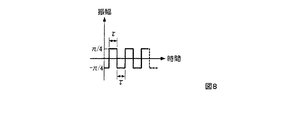
この際、CW光およびCCW光に対して位相変調が行われる。即ち、角速度入力が無い状態でCW光あるいはCCW光が光ファイバコイル5を通過する時間をτとすると、光学素子4の上で二つのルートのうち一方に設けられた位相変調器7は、タイミング信号発生回路50によって発生するタイミング信号を入力として位相変調駆動回路60が発生したパルス幅をτ、デューティ比を1/2とする矩形波(図8参照)によって、CW光とCCW光に対して+π/4と−π/4の位相変調を交互に行う。
図7に示す構成では、CW光は、光ファイバコイル5を周回する前に、位相変調器7によって位相変調を受け、CCW光は、光ファイバコイル5を周回した後に、位相変調器7によって位相変調を受ける。従って、同一時点で分岐されたCW光とCCW光とで位相変調を受ける時点がτだけずれているため、CW光とCCW光とでは相対的に+π/2と−π/2の位相差が与えられることになる。
At this time, phase modulation is performed on the CW light and the CCW light. In other words, when τ is the time during which the CW light or CCW light passes through the
In the configuration shown in FIG. 7, the CW light is phase-modulated by the
ところで、CW光とCCW光は、光ファイバコイル5を周回した後、光学素子4の光分岐結合器9によって光学的に結合し、干渉する。角速度の入力が無い状態でCW光とCCW光との間にΔφの位相差があるとすると、CW光とCCW光とが干渉した光の強度(干渉光強度I0)はその最大強度をP0として、式(1)で与えられる(図9(a)で示す実線で描かれた曲線を参照のこと)。
![]()
![]()
位相変調器7によって、CW光とCCW光に対して相対的に+π/2と−π/2の位相差が与えられると、式(1)に従い、Δφ=+π/2の場合でもΔφ=−π/2の場合でも干渉光強度I0はP0/2となる(図9(b)参照)。なお、図8に示す矩形波の立上り又は立下りの遷移時に、干渉光強度I0は最大強度P0となる点を通過するため図9(b)、図10(b)に示すスパイクノイズを生じる。
When a phase difference of + π / 2 and −π / 2 is given relative to the CW light and the CCW light by the
さて、クローズドループ方式光干渉角速度計に時計回りに角速度Ω[rad/s]が加わったとする。正確には光ファイバコイル5に時計回りに入力角速度Ωが加わることであり、この結果、CW光とCCW光とで光路長が異なり、CW光とCCW光との間に入力角速度Ωに基づく位相差が生じる(サニャック効果)。
Now, assume that an angular velocity Ω [rad / s] is added clockwise to a closed loop optical interference angular velocity meter. More precisely, the input angular velocity Ω is added to the
サニャック効果によるCW光とCCW光の位相差(サニャック位相差)をΔφsとする。時計回りの入力角速度Ωが加わった場合、CCW光の位相に対してCW光の位相はΔφsだけ進む。このサニャック位相差Δφsが加わったときの干渉光強度I0は式(2)で与えられる(図10(a)で示す実線で描かれた曲線を参照のこと。破線で示す曲線は式(1)で与えられるものである)。
![]()
![]()
入力角速度Ωが加わった場合も、位相変調器7により+π/2と−π/2の位相差が与えられることは変わらないので、CW光とCCW光とでは、位相変調器7による位相変調Δφ=±π/2とサニャック位相差Δφsが合わさった+π/2+Δφsと−π/2+Δφsの位相差が生じる。よって、CW光とCCW光の位相差が+π/2+Δφsの場合に干渉光強度I0はP1となり、−π/2+Δφsの場合に干渉光強度I0はP2となる(図10(b)参照)。P1は式(3)で与えられ、P2は式(4)で与えられる。また、干渉光強度P1と干渉光強度P2との差である干渉光強度差ΔIは式(5)で定義される。干渉光強度差ΔIの極性により、入力角速度Ωの向き(時計回り又は反時計回り)を知ることができる。

式(5)は、干渉光強度差ΔIを観測すればサニャック位相差Δφsを知ることができることを意味する。
サニャック位相差Δφsは、式(6)で与えられる。Rは、光ファイバコイル5の半径[m]、Lは光ファイバコイル5の光ファイバ長[m]、cは光速[m/s]、λは光源波長[m]、nは光ファイバコイル5のコア部の屈折率を表す。
The Sagnac phase difference Δφ s is given by equation (6). R is the radius [m] of the
クローズドループ方式光干渉角速度計では、干渉光強度差ΔIを0とするように、つまり、サニャック位相差Δφsを打ち消すように負帰還制御を行う。このことを図7を参照して説明する。
光学素子4の光分岐結合器9によってCW光とCCW光が光学的に結合した干渉光は、光カプラ3に入射して分岐される。分岐されて光カプラ3の出力となった干渉光は、受光器6に入射して光電変換される。光電変換されて生成されたアナログの電気信号は、A/D変換器25に入力され、ディジタル信号に変換される。このディジタル信号は、ディジタル信号処理装置35に入力される。
In the closed loop optical interference angular velocity meter, negative feedback control is performed so that the interference light intensity difference ΔI is 0, that is, the Sagnac phase difference Δφ s is canceled. This will be described with reference to FIG.
The interference light in which the CW light and the CCW light are optically coupled by the optical branching coupler 9 of the
ディジタル信号処理装置35は、同期検波回路36、積分器37、フィードバック信号発生回路38、ランプ波高値制御部39を含む。
A/D変換器25の出力であるディジタル信号は、同期検波回路36に入力される。同期検波回路36は、このディジタル信号に対して同期検波を行い、干渉光強度差ΔIつまりサニャック位相差Δφsに対応した信号を出力する。そして、積分器37は、同期検波回路36の出力信号を入力とし、この入力を時間積分した積分値(ディジタル値の累積加算値)を出力する。
The digital signal processing device 35 includes a
The digital signal that is the output of the A /
積分器37の出力は、フィードバック信号発生回路38に入力される。フィードバック信号発生回路38は、時間τにつきフィードバック信号の振幅をΔφsだけ増大(減少)させ、この振幅が±2mπ(mは整数)を超える時点で2mπだけ振幅を減少(増大)させるフライバック制御を繰り返し、階段状鋸歯状のフィードバック信号を発生する。なお、クローズドループ方式光干渉角速度計では負帰還制御を行うので、フィードバック信号の極性は、サニャック位相差Δφsを打ち消すように設定される。フィードバック信号の繰り返し周波数によって入力角速度を検出することができるが、このことは後述する。
The output of the
ディジタル信号処理装置35のランプ波高値制御部39は、同期検波回路36の出力とフィードバック信号発生回路38のフライバック信号に基づき、フィードバック信号発生回路38が発生するフィードバック信号の最大位相偏位φRが+2mπまたは−2mπとなるように制御を行う。
The ramp peak
フィードバック信号発生回路38の出力は、D/A変換器40に入力され、アナログ信号に変換される。このアナログ信号は、光学素子4の上で二つのルートのうち他方に設けられた位相変調器8に入力される。なお、A/D変換器25、同期検波回路36、積分器37、フィードバック信号発生回路38、D/A変換器40は、タイミング信号発生回路50が発生するタイミング信号によって信号処理の同期が保たれている。
The output of the feedback
図7に示す構成では、CW光は、光ファイバコイル5を周回した後に、位相変調器8によって位相変調を受け、CCW光は、光ファイバコイル5を周回する前に、位相変調器8によって位相変調を受ける。
In the configuration shown in FIG. 7, the CW light circulates around the
図11に、階段状鋸歯状波とされたフィードバック信号による位相変調を受けたCW光およびCCW光について、変調分の位相(変調位相)と時間との関係を例示する。両光はフライバック制御の階段状鋸歯状波とされたフィードバック信号による位相変調を受けるため、両光の変調位相は階段状鋸歯状波となる。ここで、フィードバック信号は振幅が±2mπを超える時点で2mπだけ振幅を減少(増大)させるフライバック制御を受けているため、CW光とCCW光の各変調位相は周期Tで繰り返す。
CW光の変調位相(図11(a)で実線で示されている)と、CCW光の変調位相(図11(a)で破線で示されている)とでは、位相変調を受ける時点がτだけずれているため、時間軸方向にτだけずれが生じる。ここでフィードバック信号である階段状鋸歯状波の階段の幅は時間τに設定されており、CW光の変調位相とCCW光の変調位相との位相差は、図11(b)に示されるとおりとなる。つまり、CW光とCCW光との間に−ΔφsあるいはφR(2mπ)−Δφsの位相差が与えられ、サニャック位相差Δφs(図11(a)で破線で示されている)が打ち消される。
FIG. 11 exemplifies the relationship between the phase for modulation (modulation phase) and time for CW light and CCW light that have undergone phase modulation by a feedback signal having a stepped sawtooth wave. Since both lights undergo phase modulation by a feedback signal that is a stepped sawtooth wave of flyback control, the modulation phase of both lights is a stepped sawtooth wave. Here, since the feedback signal is subjected to flyback control that decreases (increases) the amplitude by 2 mπ when the amplitude exceeds ± 2 mπ, each modulation phase of the CW light and the CCW light repeats with a period T.
In the modulation phase of the CW light (shown by a solid line in FIG. 11A) and the modulation phase of the CCW light (shown by a broken line in FIG. 11A), the time point at which the phase modulation is performed is τ Therefore, there is a shift by τ in the time axis direction. Here, the step width of the stepped sawtooth wave as the feedback signal is set to time τ, and the phase difference between the modulation phase of the CW light and the modulation phase of the CCW light is as shown in FIG. It becomes. That is, a phase difference of −Δφ s or φ R (2mπ) −Δφ s is given between the CW light and the CCW light, and a Sagnac phase difference Δφ s (shown by a broken line in FIG. 11A). Be countered.
フィードバック信号の繰り返し周波数による入力角速度の検出について説明する。フィードバック信号の繰り返し周波数f(周期T)と入力角速度Ωとの関係は、周期T=2mπτ/Δφsに式(6)を用いることで式(7)で与えられる。
すなわち、フィードバック信号の繰り返し周波数fを計測すれば与えられた入力角速度Ωを知ることができる。そこで、フィードバック信号発生回路38からのフィードバック信号を角速度出力部70に入力し、この角速度出力部70でフィードバック信号の繰り返し周波数fを求め、この繰り返し周波数fに対応した正パルス出力及び負パルス出力を生成する。正パルス出力は例えば時計回りの角速度が入力された場合の出力を示し、負パルス出力は例えば反時計回りの角速度が入力された場合の出力を示す。
That is, if the repetition frequency f of the feedback signal is measured, the given input angular velocity Ω can be known. Therefore, the feedback signal from the feedback
なお、位相変調器7が、上述の矩形波によってCW光とCCW光に対して+π/4と−π/4の位相変調を交互に行い、CW光とCCW光との間に相対的に+π/2と−π/2の位相差を与える理由は、Δφ=±π/2のとき、式(8)の干渉光強度の変化率が最大となり、サニャック位相差Δφsに対する感度が最大となるからである。
![]()
![]()
このようなクローズドループ方式光干渉角速度計として、特許文献1−4などを例示できる。
従来、クローズドループ方式光干渉角速度計では、上述したように受光器6の出力(アナログ信号)をA/D変換器25でA/D変換を行った後に、A/D変換器25が出力したディジタル信号に対して復調処理(同期検波)を行っていた。
Conventionally, in a closed loop optical interference angular velocity meter, the A /
このような構成では、受光器6の出力にランダムノイズやディジタルクロックが電気的に結合した高周波ノイズなどが重畳しており、このままA/D変換を行うため、ランダムノイズや高周波ノイズやA/D変換時のサンプリングに伴うエイリアスノイズが復調信号に含まれる。このようなノイズが、クローズドループ方式光干渉角速度計の出力誤差要因となっている。
In such a configuration, random noise, high frequency noise electrically coupled with a digital clock, or the like is superimposed on the output of the
上記ノイズを除去するために、受光器6とA/D変換器25との間にローパスフィルタを挿入することが考えられるが、この方法は、入力角速度Ωに基づく信号の周波数成分と上記ノイズの周波数成分とが近接しているため、上記ノイズを十分に減衰できず、上記誤差要因を完全に除去できるというものではない。また、上記ノイズを十分に除去できるような周波数特性の急峻なフィルタは受光器出力に波形歪みを齎すため、この波形歪に基づく復調誤差が生じるという新たな問題が惹起する。従って、受光器6とA/D変換器25との間にローパスフィルタを挿入することは、有効な手段ではない。
In order to remove the noise, it is conceivable to insert a low-pass filter between the
本発明の目的は、このような問題点に鑑み、受光器の出力に含まれるノイズに起因する出力誤差の低減を実現するクローズドループ方式光干渉角速度計を提供することである。 In view of such problems, an object of the present invention is to provide a closed loop optical interference angular velocity meter that realizes a reduction in output error due to noise included in the output of a light receiver.
上記課題を解決するために、本発明は、光源と、光ファイバコイルと、光源からの光を分岐して光ファイバコイルの両端に入射し両回り光とすると共に光ファイバコイルを伝播して回帰した当該両回り光を結合干渉させる光分岐結合器と、周期的な位相変調信号による位相差を両回り光間に与える第一の位相変調器と、光分岐結合器によって結合干渉した干渉光を分岐する光カプラと、光カプラからの干渉光の強度を電気信号に変換する受光器と、受光器からの電気信号を復調する復調部と、復調部の出力をA/D変換するA/D変換部と、A/D変換部の出力に基づき、両回り光間のサニャック位相差をゼロとするようなフィードバック信号を発生するディジタル信号処理装置と、ディジタル信号処理装置からのフィードバック信号をD/A変換するD/A変換器と、D/A変換器の出力により位相差を両回り光間に与える第二の位相変調器とを備えており、復調部は、受光器からの電気信号についてサンプルホールド処理を行う第一サンプルホールド部と、第一サンプルホールド部の出力を入力とする第一ローパスフィルタと、受光器からの電気信号についてサンプルホールド処理を行う第二サンプルホールド部と、第二サンプルホールド部の出力を入力とする第二ローパスフィルタとを備え、第一サンプルホールド部がサンプル処理を行うとき第二サンプルホールド部はホールド処理を行うとされ、第二サンプルホールド部がサンプル処理を行うとき第一サンプルホールド部はホールド処理を行うとされ、位相変調信号の周期の半分毎に、第一サンプルホールド部のサンプル処理と第二サンプルホールド部のサンプル処理とが交互に切り替わることを特徴とするクローズドループ方式光干渉角速度計とされる。 In order to solve the above-described problems, the present invention is directed to a light source, an optical fiber coil, and light from the light source branched to enter both ends of the optical fiber coil to be double-ended light and to propagate through the optical fiber coil to return. An optical branching coupler for coupling and interfering the two-way light, a first phase modulator for providing a phase difference between the two-way light by a periodic phase modulation signal, and interference light coupled and interfered by the optical branching coupler. An optical coupler that branches, a light receiver that converts the intensity of interference light from the optical coupler into an electric signal, a demodulator that demodulates the electric signal from the light receiver, and an A / D that performs A / D conversion on the output of the demodulator A digital signal processing device that generates a feedback signal that causes the Sagnac phase difference between the two-way light to be zero based on the outputs of the conversion unit and the A / D conversion unit; and the feedback signal from the digital signal processing device A D / A converter for conversion, and a second phase modulator for providing a phase difference between the two-way light by the output of the D / A converter, and the demodulator samples the electrical signal from the light receiver A first sample hold unit that performs hold processing; a first low-pass filter that receives the output of the first sample hold unit; a second sample hold unit that performs sample hold processing on an electrical signal from the light receiver; and a second sample A second low-pass filter that receives the output of the hold unit, and when the first sample hold unit performs sample processing, the second sample hold unit performs hold processing, and the second sample hold unit performs sample processing. When the first sample hold unit performs hold processing, the sample of the first sample hold unit is sampled every half of the period of the phase modulation signal. Management and the sample processing of the second sample-and-hold unit is a closed loop system optical interference gyro, characterized in that alternately switched.
このようなクローズドループ方式光干渉角速度計では、A/D変換部が、第一ローパスフィルタの出力をA/D変換する第一A/D変換器と、第二ローパスフィルタの出力をA/D変換する第二A/D変換器とを備え、ディジタル信号処理装置が、第一A/D変換器の出力から第二A/D変換器の出力を減算する減算器と、減算器の出力を積分する積分器と、積分器の出力を入力としてフィードバック信号を発生するフィードバック信号生成回路とを備える構成を採用できる。 In such a closed loop optical interference angular velocimeter, the A / D converter has a first A / D converter for A / D converting the output of the first low-pass filter, and an output of the second low-pass filter is A / D. A second A / D converter for converting, and the digital signal processing device subtracts the output of the second A / D converter from the output of the first A / D converter, and outputs the output of the subtractor. A configuration including an integrator for integration and a feedback signal generation circuit for generating a feedback signal with the output of the integrator as an input can be employed.
あるいは、このようなクローズドループ方式光干渉角速度計では、A/D変換部が、位相変調信号の周期の半分毎に、第一ローパスフィルタの出力と第二ローパスフィルタの出力を交互に選択するマルチプレクサと、マルチプレクサによって選択された出力をA/D変換するA/D変換器とを備え、ディジタル信号処理装置が、A/D変換器の出力を遅延する遅延器と、A/D変換器の出力から遅延器の出力を減算する減算器と、減算器の出力を積分する積分器と、積分器の出力を入力としてフィードバック信号を発生するフィードバック信号生成回路とを備える構成を採用できる。 Alternatively, in such a closed loop optical interference angular velocimeter, the A / D converter unit alternately selects the output of the first low-pass filter and the output of the second low-pass filter every half of the period of the phase modulation signal. And an A / D converter for A / D converting the output selected by the multiplexer, the digital signal processing device delaying the output of the A / D converter, and the output of the A / D converter It is possible to employ a configuration including a subtracter that subtracts the output of the delay device from the integrator, an integrator that integrates the output of the subtractor, and a feedback signal generation circuit that generates a feedback signal with the output of the integrator as an input.
本発明によれば、受光器からの電気信号を、二系統(第一サンプルホールド部と第二サンプルホールド部)に分け、第一位相変調器で用いた位相変調信号の周期の半分毎にサンプル処理とホールド処理を交互に切り替えるから、各系統のサンプルホールド部の出力の周波数成分は直流近傍となる。従って、各系統のサンプルホールド部の出力に対して適用する第一ローパスフィルタおよび第二ローパスフィルタは、受光器の出力に含まれるノイズを十分に除去できるような特性のフィルタが可能になる。このため、受光器の出力に含まれるノイズを十分に除去でき、クローズドループ方式光干渉角速度計の出力誤差が低減する。 According to the present invention, the electric signal from the light receiver is divided into two systems (first sample hold unit and second sample hold unit), and sampled every half of the period of the phase modulation signal used in the first phase modulator. Since the processing and the hold processing are alternately switched, the frequency component of the output of the sample hold unit of each system is close to the direct current. Therefore, the first low-pass filter and the second low-pass filter applied to the output of the sample hold unit of each system can be a filter having a characteristic that can sufficiently remove noise included in the output of the light receiver. For this reason, the noise contained in the output of the light receiver can be sufficiently removed, and the output error of the closed loop optical interference angular velocity meter is reduced.
図面を参照して、本発明の実施形態を説明する。
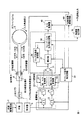
図1は、本発明であるクローズドループ方式光干渉角速度計の一実施形態の構成を示している。図7に示す従来のクローズドループ方式光干渉角速度計の構成要素と同一の構成要素には同じ符号を割り当てて説明を省略する。
Embodiments of the present invention will be described with reference to the drawings.
FIG. 1 shows a configuration of an embodiment of a closed loop optical interference angular velocity meter according to the present invention. The same components as those of the conventional closed-loop optical interference angular velocity meter shown in FIG.
受光器6からの電気信号は、復調部10の入力となる。この復調部10は、受光器6からの電気信号についてサンプルホールド処理を行う第一サンプルホールド部11と、第一サンプルホールド部11の出力を入力とする第一ローパスフィルタ13と、受光器6からの電気信号についてサンプルホールド処理を行う第二サンプルホールド部12と、第二サンプルホールド部12の出力を入力とする第二ローパスフィルタ14とを含んで構成されている。
The electric signal from the
第一サンプルホールド部11と第二サンプルホールド部12は、タイミング信号発生回路50が発生するタイミング信号によって信号処理の同期が保たれている。
The first
第一サンプルホールド部11と第二サンプルホールド部12の各処理を図2と図3を参照して説明する。
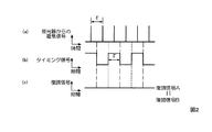
入力角速度が無い場合、図9(b)に示す干渉光強度に対応した電気信号波形は図2(a)に示すとおりとなる。図2(a)の縦軸は受光器6からの電気信号の振幅、横軸は時間を表す。第一サンプルホールド部11と第二サンプルホールド部12に入力されるタイミング信号は、図2(b)に示すように、位相変調器7に入力される位相変調信号に対して位相がπ/2ずれた矩形波とされる。図2(b)の縦軸は振幅、横軸は時間を表す。
Each process of the 1st sample hold
When there is no input angular velocity, the electrical signal waveform corresponding to the interference light intensity shown in FIG. 9B is as shown in FIG. In FIG. 2A, the vertical axis represents the amplitude of the electric signal from the
そして、第一サンプルホールド部11はタイミング信号の立上り時点でサンプル処理を行いこの値をホールドし、第二サンプルホールド部12はタイミング信号の立下り時点でサンプル処理を行いこの値をホールドする。タイミング信号の周期は、位相変調器7に入力される位相変調信号である矩形波の周期と同じであり、第一サンプルホールド部11によるサンプル処理と第二サンプルホールド部12によるサンプル処理は、タイミング信号の周期の半分毎に交互に切り替わるようにして行われる。また、第一サンプルホールド部11がサンプル処理を行うときは、第二サンプルホールド部12はホールド処理を持続しており、第二サンプルホールド部12がサンプル処理を行うときは、第一サンプルホールド部11はホールド処理を持続している。
The first
このため、入力角速度が無い場合、第一サンプルホールド部11の出力である復調信号Aと第二サンプルホールド部12の出力である復調信号Bは、図2(c)に示すとおり、同じ大きさとなる。図2(c)の縦軸は復調信号の大きさ、横軸は時間を表す。
Therefore, when there is no input angular velocity, the demodulated signal A output from the first
入力角速度Ωが有る場合、図10(b)に示す干渉光強度に対応した電気信号波形は図3(a)に示すとおりとなる。第一サンプルホールド部11と第二サンプルホールド部12に入力されるタイミング信号は、図3(b)に示すように、入力角速度が無い場合と同じである。よって、タイミング信号に従って第一サンプルホールド部11と第二サンプルホールド部12が動作すると、第一サンプルホールド部11による復調信号Aと第二サンプルホールド部12による復調信号Bは、図3(c)に示すとおり、異なる大きさとなる。復調信号Aの大きさは、図10(b)に示す干渉光強度P1に、復調信号Bの大きさは、図10(b)に示す干渉光強度P2に、それぞれ対応する。
When there is an input angular velocity Ω, the electrical signal waveform corresponding to the interference light intensity shown in FIG. 10B is as shown in FIG. The timing signals input to the first
第一サンプルホールド部11の出力である復調信号Aは、第一ローパスフィルタ13の入力となる。また、第二サンプルホールド部12の出力である復調信号Bは、第二ローパスフィルタ14の入力となる。図2(c)および図3(c)を参照して明らかなように、第一サンプルホールド部11による復調信号Aと第二サンプルホールド部12による復調信号Bの各周波数成分は直流近傍であるから、第一ローパスフィルタ13と第二ローパスフィルタ14として、受光器6の出力に含まれるノイズを十分に除去できるような特性のローパスフィルタを用いることができる。
The demodulated signal A that is the output of the first
第一ローパスフィルタ13の出力は、A/D変換部20に含まれる第一A/D変換器21の入力となりA/D変換が行われる。また、第二ローパスフィルタ14の出力は、A/D変換部20に含まれる第二A/D変換器22の入力となりA/D変換が行われる。第一A/D変換器21と第二A/D変換器22は、タイミング信号発生回路50が発生するタイミング信号によって信号処理の同期が保たれている。
The output of the first low-
第一A/D変換器21と第二A/D変換器22の各出力は、ディジタル信号処理装置30に含まれる減算器31に入力され、減算器31は、第一A/D変換器21の出力から第二A/D変換器22の出力を減算して、この結果を出力する。減算器31の出力はディジタル信号処理装置30に含まれる積分器37に入力される。
積分器37以降の処理は従来と同様である。
The outputs of the first A /
The processing after the
<変形例>
既述の実施形態の変形例を説明する。
既述の実施形態では、従来例との対比から、ディジタル信号処理装置30にランプ波高値制御部39を含む構成を示した(図1参照)。しかし、フィードバック信号発生回路38が発生するフィードバック信号の最大振幅を動的に制御することなく一定に設定する場合にはランプ波高値制御部39を設ける必要が無い。ランプ波高値制御部39を設けない場合の構成を図4に示す。
<Modification>
A modification of the above-described embodiment will be described.
In the embodiment described above, the configuration in which the digital signal processing device 30 includes the ramp peak
また、本発明の要諦をなす既述の構成は、角速度出力部70が積分器37の出力から角速度出力を求めてこれを出力する構成にも適用できる(図5参照)。
The above-described configuration that forms the gist of the present invention can also be applied to a configuration in which the angular
また、既述の実施形態と同様の作用を齎す構成として、A/D変換部20とディジタル信号処理装置30を図6に示す構成とすることもできる。即ち、A/D変換部20を、位相変調信号の周期の半分毎に、第一ローパスフィルタ13の出力と第二ローパスフィルタ14の出力を交互に選択するマルチプレクサ23と、マルチプレクサ23によって選択された出力をA/D変換するA/D変換器24とを含む構成とする。マルチプレクサ23とA/D変換器24はタイミング信号発生回路50が発生するタイミング信号によって信号処理の同期が保たれている。また、ディジタル信号処理装置30は、A/D変換器24の出力を遅延する遅延器33をさらに含んで構成される。この構成では、第一ローパスフィルタ13の出力と第二ローパスフィルタ14の出力が交互にA/D変換されてディジタル信号処理装置30に入力されるから、遅延器33はいずれか一方(この例では、第二ローパスフィルタ14の出力である)の出力を遅延させる。遅延時間はτに設定される。
Further, as a configuration that exhibits the same operation as that of the above-described embodiment, the A / D conversion unit 20 and the digital signal processing device 30 may be configured as shown in FIG. That is, the A / D converter 20 is selected by the
A/D変換器24の出力と遅延器33の出力は、ディジタル信号処理装置30に含まれる減算器31に入力され、減算器31は、A/D変換器24の出力から遅延器33の出力を減算して、この結果を出力する。減算器31の出力はディジタル信号処理装置30に含まれる積分器37に入力される。
積分器37以降の処理は従来と同様である。
The output of the A /
The processing after the
以上の実施形態の他、本発明であるクローズドループ方式光干渉角速度計は上述の実施形態に限定されるものではなく、本発明の趣旨を逸脱しない範囲で適宜変更が可能である。 In addition to the above-described embodiments, the closed-loop optical interference angular velocity meter according to the present invention is not limited to the above-described embodiments, and can be appropriately changed without departing from the gist of the present invention.
2 光源
3 光カプラ
4 光学素子
5 光ファイバコイル
6 受光器
7 位相変調器
8 位相変調器
9 光分岐結合器
10 復調部
11 第一サンプルホールド部
12 第二サンプルホールド部
13 第一ローパスフィルタ
14 第二ローパスフィルタ
20 A/D変換部
21 第一A/D変換器
22 第二A/D変換器
23 マルチプレクサ
24 A/D変換器
30 ディジタル信号処理装置
31 減算器
37 積分器
38 フィードバック信号発生器
39 ランプ波高値制御部
40 D/A変換器
50 タイミング信号発生回路
60 位相変調駆動回路
70 角速度出力部
2 light source 3
Claims (3)
光源と、
光ファイバコイルと、
上記光源からの光を分岐して上記光ファイバコイルの両端に入射し両回り光とすると共に上記光ファイバコイルを伝播して回帰した当該両回り光を結合干渉させる光分岐結合器と、
周期的な位相変調信号による位相差を上記両回り光間に与える第一の位相変調器と、
上記光分岐結合器によって結合干渉した干渉光を分岐する光カプラと、
上記光カプラからの干渉光の強度を電気信号に変換する受光器と、
上記受光器からの電気信号を復調する復調部と、
上記復調部の出力をA/D変換するA/D変換部と、
上記A/D変換部の出力に基づき、上記両回り光間のサニャック位相差をゼロとするようなフィードバック信号を発生するディジタル信号処理装置と、
上記ディジタル信号処理装置からのフィードバック信号をD/A変換するD/A変換器と、
上記D/A変換器の出力により位相差を上記両回り光間に与える第二の位相変調器とを備え、
上記復調部は、
上記受光器からの電気信号についてサンプルホールド処理を行う第一サンプルホールド部と、
上記第一サンプルホールド部の出力を入力とする第一ローパスフィルタと、
上記受光器からの電気信号についてサンプルホールド処理を行う第二サンプルホールド部と、
上記第二サンプルホールド部の出力を入力とする第二ローパスフィルタとを備え、
上記第一サンプルホールド部がサンプル処理を行うとき上記第二サンプルホールド部はホールド処理を行うとされ、上記第二サンプルホールド部がサンプル処理を行うとき上記第一サンプルホールド部はホールド処理を行うとされ、上記位相変調信号の周期の半分毎に、上記第一サンプルホールド部のサンプル処理と上記第二サンプルホールド部のサンプル処理とが交互に切り替わる
ことを特徴とするクローズドループ方式光干渉角速度計。 In a closed loop optical interference angular velocimeter that detects the angular velocity by performing feedback control so that the phase change of light (Sagnac phase difference) based on the Sagnac effect caused by the angular velocity is zero,
A light source;
An optical fiber coil;
An optical branching coupler for branching the light from the light source and entering both ends of the optical fiber coil to make double-ended light and coupling and interfering with the double-ended light propagating through the optical fiber coil and returning;
A first phase modulator that provides a phase difference due to a periodic phase modulation signal between the light beams;
An optical coupler for branching interference light coupled and interfered by the optical branching coupler;
A light receiver for converting the intensity of the interference light from the optical coupler into an electrical signal;
A demodulator that demodulates the electrical signal from the light receiver;
An A / D converter for A / D converting the output of the demodulator;
A digital signal processing device that generates a feedback signal based on the output of the A / D converter so that the Sagnac phase difference between the two-way light is zero;
A D / A converter for D / A converting the feedback signal from the digital signal processing device;
A second phase modulator that provides a phase difference between the two-way light by the output of the D / A converter,
The demodulator
A first sample and hold unit that performs a sample and hold process on the electrical signal from the light receiver;
A first low-pass filter that receives the output of the first sample-and-hold unit, and
A second sample and hold unit that performs a sample and hold process on the electrical signal from the light receiver;
A second low-pass filter having the output of the second sample-and-hold unit as an input,
When the first sample hold unit performs sample processing, the second sample hold unit performs hold processing. When the second sample hold unit performs sample processing, the first sample hold unit performs hold processing. A closed-loop optical interference angular velocity meter, wherein the sample processing of the first sample hold unit and the sample processing of the second sample hold unit are alternately switched every half of the period of the phase modulation signal.
上記第一ローパスフィルタの出力をA/D変換する第一A/D変換器と、
上記第二ローパスフィルタの出力をA/D変換する第二A/D変換器とを備え、
上記ディジタル信号処理装置は、
上記第一A/D変換器の出力から上記第二A/D変換器の出力を減算する減算器と、
上記減算器の出力を積分する積分器と、
上記積分器の出力を入力として上記フィードバック信号を発生するフィードバック信号生成回路とを備える
ことを特徴とする請求項1に記載のクローズドループ方式光干渉角速度計。 The A / D converter is
A first A / D converter for A / D converting the output of the first low-pass filter;
A second A / D converter for A / D converting the output of the second low-pass filter,
The digital signal processor is
A subtractor for subtracting the output of the second A / D converter from the output of the first A / D converter;
An integrator for integrating the output of the subtractor;
The closed-loop optical interference angular velocity meter according to claim 1, further comprising: a feedback signal generation circuit that generates the feedback signal with the output of the integrator as an input.
上記位相変調信号の周期の半分毎に、上記第一ローパスフィルタの出力と上記第二ローパスフィルタの出力を交互に選択するマルチプレクサと、
上記マルチプレクサによって選択された上記出力をA/D変換するA/D変換器とを備え、
上記ディジタル信号処理装置は、
上記A/D変換器の出力を遅延する遅延器と、
上記A/D変換器の出力から上記遅延器の出力を減算する減算器と、
上記減算器の出力を積分する積分器と、
上記積分器の出力を入力として上記フィードバック信号を発生するフィードバック信号生成回路とを備える
ことを特徴とする請求項1に記載のクローズドループ方式光干渉角速度計。 The A / D converter is
A multiplexer that alternately selects the output of the first low-pass filter and the output of the second low-pass filter for each half of the period of the phase modulation signal;
An A / D converter for A / D converting the output selected by the multiplexer;
The digital signal processor is
A delay device for delaying the output of the A / D converter;
A subtractor for subtracting the output of the delay device from the output of the A / D converter;
An integrator for integrating the output of the subtractor;
The closed-loop optical interference angular velocity meter according to claim 1, further comprising: a feedback signal generation circuit that generates the feedback signal with the output of the integrator as an input.
Priority Applications (1)
| Application Number | Priority Date | Filing Date | Title |
|---|---|---|---|
| JP2008181048A JP4922256B2 (en) | 2008-07-11 | 2008-07-11 | Closed loop optical interference angular velocity meter |
Applications Claiming Priority (1)
| Application Number | Priority Date | Filing Date | Title |
|---|---|---|---|
| JP2008181048A JP4922256B2 (en) | 2008-07-11 | 2008-07-11 | Closed loop optical interference angular velocity meter |
Publications (2)
| Publication Number | Publication Date |
|---|---|
| JP2010019717A true JP2010019717A (en) | 2010-01-28 |
| JP4922256B2 JP4922256B2 (en) | 2012-04-25 |
Family
ID=41704774
Family Applications (1)
| Application Number | Title | Priority Date | Filing Date |
|---|---|---|---|
| JP2008181048A Active JP4922256B2 (en) | 2008-07-11 | 2008-07-11 | Closed loop optical interference angular velocity meter |
Country Status (1)
| Country | Link |
|---|---|
| JP (1) | JP4922256B2 (en) |
Citations (2)
| Publication number | Priority date | Publication date | Assignee | Title |
|---|---|---|---|---|
| JP2002500376A (en) * | 1997-12-31 | 2002-01-08 | ハネウエル インコーポレーテツド | Fiber optic gyroscope |
| JP2006177893A (en) * | 2004-12-24 | 2006-07-06 | Japan Aviation Electronics Industry Ltd | Optical interference angular velocimeter |
-
2008
- 2008-07-11 JP JP2008181048A patent/JP4922256B2/en active Active
Patent Citations (2)
| Publication number | Priority date | Publication date | Assignee | Title |
|---|---|---|---|---|
| JP2002500376A (en) * | 1997-12-31 | 2002-01-08 | ハネウエル インコーポレーテツド | Fiber optic gyroscope |
| JP2006177893A (en) * | 2004-12-24 | 2006-07-06 | Japan Aviation Electronics Industry Ltd | Optical interference angular velocimeter |
Also Published As
| Publication number | Publication date |
|---|---|
| JP4922256B2 (en) | 2012-04-25 |
Similar Documents
| Publication | Publication Date | Title |
|---|---|---|
| JP5362180B2 (en) | Asynchronous demodulation of fiber optic gyroscope | |
| EP1835258B1 (en) | Digital feedback method for optical gyroscopes | |
| CN110360998B (en) | Detection system and method of resonant optical gyroscope based on pulse light detection | |
| CN110360997B (en) | Detection system and method of time division multiplexing resonant optical gyroscope | |
| JP2007163941A (en) | Four-phase phase modulation circuit | |
| EP1701186A1 (en) | Electro-optic delay line discriminator | |
| JP3808820B2 (en) | Optical sampling method, apparatus and program | |
| CN102636187A (en) | Highly reciprocal resonant mode fiber-optic gyroscope detection device and method | |
| US20080218765A1 (en) | Signal Processing For A Sagnac Interferometer | |
| JP2010281819A (en) | Method and amplifying stage for suppressing modulation distortion rate sensing errors in resonator fiber optic gyroscope | |
| JP4922256B2 (en) | Closed loop optical interference angular velocity meter | |
| US5767969A (en) | Gyrometric detection method and sampled optical gyrometer to implement said method | |
| JP4847512B2 (en) | Closed loop optical interference angular velocity meter | |
| JP5654823B2 (en) | System to reduce gyroscope error with limited power quality in fiber optic gyroscope | |
| JP2532326B2 (en) | Optical interference gyro | |
| RU2227272C2 (en) | Wide-range fiber-optical meter of angular velocity | |
| JP2008154230A (en) | Opto-electrical oscillator clock with optical distribution circuit network | |
| JPH04223213A (en) | Light interference angular velocity meter | |
| CN117705079A (en) | Device and method for suppressing noise of wide-spectrum light source resonant fiber-optic gyroscope | |
| JP2003149083A (en) | Method and apparatus for measuring wavelength dispersion | |
| CN116124116A (en) | Optical fiber gyroscope and comb pulse error suppression system and method | |
| CN115752418A (en) | Random walk improvement method for resonant fiber optic gyroscope based on wide-spectrum light source | |
| JP2009092382A (en) | Closed loop type optical interference angular velocity meter | |
| JP2005265681A (en) | Closed loop system optical fiber gyro | |
| JP2001021363A (en) | Light interference angular speed meter |
Legal Events
| Date | Code | Title | Description |
|---|---|---|---|
| A621 | Written request for application examination |
Free format text: JAPANESE INTERMEDIATE CODE: A621 Effective date: 20100405 |
|
| TRDD | Decision of grant or rejection written | ||
| A01 | Written decision to grant a patent or to grant a registration (utility model) |
Free format text: JAPANESE INTERMEDIATE CODE: A01 Effective date: 20120124 |
|
| A01 | Written decision to grant a patent or to grant a registration (utility model) |
Free format text: JAPANESE INTERMEDIATE CODE: A01 |
|
| A61 | First payment of annual fees (during grant procedure) |
Free format text: JAPANESE INTERMEDIATE CODE: A61 Effective date: 20120203 |
|
| R150 | Certificate of patent or registration of utility model |
Ref document number: 4922256 Country of ref document: JP Free format text: JAPANESE INTERMEDIATE CODE: R150 Free format text: JAPANESE INTERMEDIATE CODE: R150 |
|
| FPAY | Renewal fee payment (event date is renewal date of database) |
Free format text: PAYMENT UNTIL: 20150210 Year of fee payment: 3 |
|
| R250 | Receipt of annual fees |
Free format text: JAPANESE INTERMEDIATE CODE: R250 |
|
| R250 | Receipt of annual fees |
Free format text: JAPANESE INTERMEDIATE CODE: R250 |
|
| R250 | Receipt of annual fees |
Free format text: JAPANESE INTERMEDIATE CODE: R250 |
|
| R250 | Receipt of annual fees |
Free format text: JAPANESE INTERMEDIATE CODE: R250 |
|
| R250 | Receipt of annual fees |
Free format text: JAPANESE INTERMEDIATE CODE: R250 |
|
| R250 | Receipt of annual fees |
Free format text: JAPANESE INTERMEDIATE CODE: R250 |
|
| R250 | Receipt of annual fees |
Free format text: JAPANESE INTERMEDIATE CODE: R250 |
|
| R250 | Receipt of annual fees |
Free format text: JAPANESE INTERMEDIATE CODE: R250 |
|
| R250 | Receipt of annual fees |
Free format text: JAPANESE INTERMEDIATE CODE: R250 |
|
| R250 | Receipt of annual fees |
Free format text: JAPANESE INTERMEDIATE CODE: R250 |