JP2010019555A - Gas sensor - Google Patents
Gas sensor Download PDFInfo
- Publication number
- JP2010019555A JP2010019555A JP2008177498A JP2008177498A JP2010019555A JP 2010019555 A JP2010019555 A JP 2010019555A JP 2008177498 A JP2008177498 A JP 2008177498A JP 2008177498 A JP2008177498 A JP 2008177498A JP 2010019555 A JP2010019555 A JP 2010019555A
- Authority
- JP
- Japan
- Prior art keywords
- gas
- sensitive layer
- conductivity type
- gas sensor
- side electrode
- Prior art date
- Legal status (The legal status is an assumption and is not a legal conclusion. Google has not performed a legal analysis and makes no representation as to the accuracy of the status listed.)
- Granted
Links
Images


Abstract
Description
本発明は、ガスセンサに関し、より具体的には、自動車等の排気経路に取り付けられる、耐久性に優れたガスセンサに関するものである。 The present invention relates to a gas sensor, and more specifically to a gas sensor with excellent durability that is attached to an exhaust path of an automobile or the like.
自動車分野では、排ガス規制や燃費向上のためのエンジン制御の高精度化や、車室内外の気体成分の把握のため、信頼性が高く、高感度のガスセンサが要求されている。自動車の空燃比センサとして使用されている安定化ジルコニアを用いた酸素センサや、一般に普及している金属酸化物半導体を用いた電気抵抗式ガスセンサは、信頼性に優れるが、感度や応答速度が低いという課題を有している。一方、感度および応答速度を兼備するガスセンサとして、MOSFET(Metal Oxide Semiconductor Field Effect Transistor)と酸化物半導体等とを組み合わせたMOSFET式センサが知られている(非特許文献1)。また、このMOSFET式センサとしては、イオン導電性酸素酸塩とMOSFETとを組み合わせたセンサの提案もなされている(特許文献1)。 In the automobile field, a highly reliable and highly sensitive gas sensor is required to improve the accuracy of engine control for exhaust gas regulation and fuel efficiency improvement and to grasp the gas components inside and outside the vehicle interior. Oxygen sensors using stabilized zirconia, which is used as an air-fuel ratio sensor for automobiles, and electric resistance gas sensors using metal oxide semiconductors, which are widely used, are excellent in reliability, but have low sensitivity and response speed It has a problem. On the other hand, as a gas sensor having both sensitivity and response speed, a MOSFET sensor in which a MOSFET (Metal Oxide Semiconductor Field Effect Transistor) is combined with an oxide semiconductor or the like is known (Non-Patent Document 1). As this MOSFET type sensor, a sensor combining an ion conductive oxyacid salt and a MOSFET has also been proposed (Patent Document 1).
上記のMOSFET式のガスセンサでは、電子流を制御するチャネルが半導体基板の表面に位置するので、高温の雰囲気ガスに暴露されやすい。このため長期信頼性を確保する上で問題がある。また、SiCなどの半導体表面では界面順位密度にばらつきが生じやすくセンサ特性が不安定化する結果、製造の歩留りが低下する。さらに、チャネルが半導体表面に位置するため、界面準位の影響を受けることで、応答速度が遅くなるという短所をもつ。そこで、本発明は、性能が長期間安定して維持され、特性が安定して製造歩留りの低下が抑止され、応答速度が大きいガスセンサを提供することを目的とする。 In the above-described MOSFET type gas sensor, since the channel for controlling the electron flow is located on the surface of the semiconductor substrate, it is easily exposed to a high-temperature ambient gas. Therefore, there is a problem in ensuring long-term reliability. In addition, the semiconductor surface such as SiC tends to vary in the interface order density, and the sensor characteristics become unstable, resulting in a decrease in manufacturing yield. Further, since the channel is located on the semiconductor surface, it has a disadvantage that the response speed becomes slow due to the influence of the interface state. Therefore, an object of the present invention is to provide a gas sensor that maintains its performance stably for a long period of time, stabilizes its characteristics, suppresses a decrease in manufacturing yield, and has a high response speed.
本発明のガスセンサは、第1導電型の半導体基板と、第1導電型半導体基板の表面から内部へと設けられた第2導電型領域と、第2導電型領域の表面に電気的に接続されたガス感応層と、ガス感応層の上に位置して電気的に接続された第2導電側電極と、第2導電型領域を挟むように、表面に設けられた、ソース電極およびドレイン電極と、半導体基板の中で第2導電側領域に接し、ソース電極とドレイン電極とを連絡する、第1導電型の通路と、第1導電型の通路に連絡している表面または裏面に電気的に接続された第1導電側電極とを備える。そして、ガス感応層を介在させて、第1導電側電極と第2導電側電極との間に電圧を加えて、第2導電側領域と第1導電型の通路とのpn接合に逆バイアス電圧を印加することを特徴とする。 The gas sensor of the present invention is electrically connected to the first conductive type semiconductor substrate, the second conductive type region provided from the surface of the first conductive type semiconductor substrate to the inside, and the surface of the second conductive type region. A gas sensitive layer, a second conductive side electrode located on and electrically connected to the gas sensitive layer, and a source electrode and a drain electrode provided on the surface so as to sandwich the second conductive type region, Electrically connecting the first conductivity type passage in contact with the second conductive side region in the semiconductor substrate and connecting the source electrode and the drain electrode, and the front or back surface in communication with the first conductivity type passage. And a connected first conductive side electrode. Then, a voltage is applied between the first conductive side electrode and the second conductive side electrode through the gas sensitive layer, and a reverse bias voltage is applied to the pn junction between the second conductive side region and the first conductive type passage. Is applied.
上記の構造では、第2導電型領域の先の半導体基板の内部に、第1導電型の通路(チャネル)が位置し、第2導電型領域とチャネルとの界面にpn接合が形成される。第1導電側電極と第2導電側電極との間に電圧をかけて、このpn接合に逆バイアス電圧を、常時、かけておく。ガス感応層にガス吸着が生じると、電気抵抗が変動するので、常時印加されているpn接合への逆バイアス電圧が変動し、空乏層の張り出しが変化してチャネル断面を変化させる。このため、ガス吸着量の変化によって、キャリアがチャネルを通る通りやすさが変化し、ソース/ドレイン電極間の電流値の変化となって現れる。これによって、高い応答速度、および高い感度で、ガス吸着量を検知することができる。また、チャネルは、半導体基板の内部に位置するので、ガスに暴露されず、長期信頼性が劣化することはない。チャネルが界面準位の影響を受けないので、特性が安定して、製造歩留りが低下することはない。上記の構造の場合、キャリアは、チャネルを半導体基板に板面に沿う方向に流れる。 In the above structure, the first conductivity type passage (channel) is located inside the semiconductor substrate ahead of the second conductivity type region, and a pn junction is formed at the interface between the second conductivity type region and the channel. A voltage is applied between the first conductive side electrode and the second conductive side electrode, and a reverse bias voltage is always applied to the pn junction. When gas adsorption occurs in the gas sensitive layer, the electric resistance fluctuates, so that the reverse bias voltage to the pn junction that is constantly applied fluctuates, and the overhang of the depletion layer changes to change the channel cross section. For this reason, the change in gas adsorption amount changes the ease with which carriers pass through the channel, and appears as a change in the current value between the source and drain electrodes. Thereby, the gas adsorption amount can be detected with high response speed and high sensitivity. Further, since the channel is located inside the semiconductor substrate, it is not exposed to gas and long-term reliability is not deteriorated. Since the channel is not affected by the interface state, the characteristics are stable and the manufacturing yield does not decrease. In the case of the above structure, the carrier flows in the direction along the plate surface of the channel on the semiconductor substrate.
本発明の他のガスセンサは、第1導電型の半導体基板と、半導体基板の、表面に位置するソース電極、および裏面に位置するドレイン電極と、ソース電極とドレイン電極とを連絡している第1導電型の通路を、取り囲むように設けられ、表面または裏面に露出する第2導電型領域と、露出した第2導電型領域に電気的に接続されたガス感応層と、ガス感応層の上に位置して電気的に接続された第2導電側電極と、第1導電型の通路に連絡している表面または裏面に電気的に接続された第1導電側電極とを備える。そして、ガス感応層を介在させて、第1導電側電極と第2導電側電極との間に電圧を加えて、第1導電側領域の通路の周りのpn接合に逆バイアス電圧を印加することを特徴とする。 According to another gas sensor of the present invention, a first conductivity type semiconductor substrate, a source electrode located on the front surface of the semiconductor substrate, a drain electrode located on the back surface, and a first electrode that communicates the source electrode and the drain electrode. A conductive type passage is provided so as to surround the second conductive type region exposed on the front surface or the back surface, a gas sensitive layer electrically connected to the exposed second conductive type region, and a gas sensitive layer on the gas sensitive layer A second conductive side electrode positioned and electrically connected; and a first conductive side electrode electrically connected to a front surface or a back surface communicating with the first conductive type passage. Then, a reverse bias voltage is applied to the pn junction around the passage in the first conductive side region by applying a voltage between the first conductive side electrode and the second conductive side electrode through the gas sensitive layer. It is characterized by.
上記の構造によれば、チャネル(通路)は半導体基板を貫通する方向に沿って形成される。そのチャネルを取り囲むpn接合から張り出す空乏層は、ガス感応層でのガス吸着量によって、張り出す大きさが変化し、ソース/ドレイン電極間を流れる電流の変化となって現れる。このため、この構造においても、応答速度は高く、感度も十分高い。また、チャネルは半導体基板の内部に、半導体基板を貫通するように設けられるので、ガスに暴露されることはなく、長期信頼性を確保することができる。また、チャネルが界面準位の影響を受けないので、特性が安定して、製造歩留りが低下することはない。この場合、キャリアは、チャネルを半導体基板に板面に直交する方向に流れる。 According to the above structure, the channel (passage) is formed along the direction penetrating the semiconductor substrate. The depletion layer protruding from the pn junction surrounding the channel changes in size depending on the amount of gas adsorbed in the gas sensitive layer, and appears as a change in the current flowing between the source / drain electrodes. For this reason, even in this structure, the response speed is high and the sensitivity is sufficiently high. Further, since the channel is provided inside the semiconductor substrate so as to penetrate the semiconductor substrate, it is not exposed to gas and long-term reliability can be ensured. Further, since the channel is not affected by the interface state, the characteristics are stable and the manufacturing yield does not decrease. In this case, the carrier flows through the channel in the direction perpendicular to the plate surface of the semiconductor substrate.
上記のガス感応層を、酸化物半導体、イオン導電性酸素酸塩、または固体電解質とイオン導電性酸素酸塩との組み合わせ、のいずれかとすることができる。これによって、感度が高く、応答速度の大きいガスセンサを提供することができる。 The gas sensitive layer can be either an oxide semiconductor, an ion conductive oxyacid salt, or a combination of a solid electrolyte and an ion conductive oxyacid salt. As a result, a gas sensor with high sensitivity and high response speed can be provided.
上記の感応層に、感度を高めるために増感剤を含ませることができる。これによって、ガス選択性を高め、ガスが非常に低濃度であっても、その濃度を精度よく検知することができる。増感剤は、検知ガスおよび感応層の種類に応じて決まっており、このあとで詳述する。 A sensitizer can be included in the sensitive layer to increase sensitivity. As a result, the gas selectivity can be improved and the concentration can be accurately detected even if the gas has a very low concentration. The sensitizer is determined according to the type of the detection gas and the sensitive layer, and will be described in detail later.
上記のガス感応層を、多孔質とすることができる。これによって、第2導電側電極の下に位置するガス感応層に、十分な表面積のガス吸着部分を持たせることができる。 The gas sensitive layer can be porous. Thereby, the gas-sensitive layer located under the second conductive side electrode can have a gas adsorption portion having a sufficient surface area.
本発明のガスセンサは、チャネルはガスに暴露されないので性能が長期間安定して維持され、界面順位の影響を受けないので特性が安定して製造歩留り低下は生じず、また応答速度は大きい。 In the gas sensor of the present invention, since the channel is not exposed to the gas, the performance is stably maintained for a long period of time, and the performance is not affected by the interface order, so that the characteristics are stable and the production yield is not lowered, and the response speed is high.
(実施の形態1)
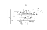
図1は、本発明の実施の形態1におけるガスセンサ10を示す図である。このガスセンサ10は、n型SiC基板1の表面側に、ガス分子が吸着すると電気抵抗が変化する触媒層3が設けられ、その下にp型領域6が形成されている。本実施の形態では、ガス感応層に、酸化物半導体の触媒3を用いている。p型領域6の深さ方向の先端は、n型SiC基板との間にpn接合15を形成し。その下(SiC基板の内部)に、n型チャネル5を形成している。n型チャネル5を上下から挟むように、チャネル5の裏面側にも、p型領域6が設けられている。n型チャネル5の領域のSiC基板1の裏面から表面にかけて、次の部分が形成されている。
(裏面p側電極11b/p型領域6/n型チャネル5/p型領域6/触媒層3/表面p側電極11a)
表面p側電極11aおよび裏面p側電極11bは、ともに定電圧電源9のマイナス電極に接続されて同電位とされている。定電圧電源のプラス電極は、n型SiC基板のn型領域に接続されている。このため、上記の2つのp型領域6とn型領域との間に形成されるpn接合15には、逆バイアス電圧が印加される。なお、上記のn型SiC基板において、n型領域のn型キャリア濃度は、逆バイアス電圧の印加による空乏層の張り出しをチャネル5の側に大きくするために、p型領域6のp型キャリア濃度よりも小さいことが望ましい。したがってn型SiC基板は、n−SiC基板1とするのがよい。また、使用する温度域によるが、以下の説明では、半導体基板がSiC基板の場合について説明するが、シリコン基板など他の半導体基板を用いてもよい。
(Embodiment 1)
FIG. 1 is a diagram showing a
(Back surface p-
Both the front surface p-
SiC基板1の表面側に、p型領域6を挟むように、ソース電極21およびドレイン電極22が設けられている。電位VDのドレイン電極22からは、n型チャネル5を通って、定常的に、電流IDがソース電極21へと流れるようにされている。電流IDのキャリアは電子であり、接地電位のソース電極21側から、電子がn型チャネル5を通って、電位VDのドレイン電極22側へ流れることで、電流IDがドレインからソースへと流れることになる。
A
上記の表面側の触媒層3は、酸化物半導体のWO3などから形成されており、検知対象のガスが吸着すると電気抵抗が変化する。触媒層3は、検知対象ガスに応じて、そのガスの選択性が高いものを用いる。触媒3のガス選択性を高めるために、その触媒3および検知対象ガスに対応した増感剤を添加することが、通常、行われる。表1に、検知対象ガスと、そのガスに対する選択性をもつ触媒(感応剤)3を示す。また、増感剤を添加することが普通に行われる触媒3については、増感剤も合わせて示す。本発明の実施の形態では、少なくとも、表1に示す検知対象ガス、触媒3、増感剤を用いる。その他の、ガスを検知対象にして、その他の触媒3、増感剤を用いてもよい。 The catalyst layer 3 on the surface side is formed of WO 3 or the like of an oxide semiconductor, and the electric resistance changes when the gas to be detected is adsorbed. As the catalyst layer 3, a gas having high gas selectivity is used in accordance with the detection target gas. In order to increase the gas selectivity of the catalyst 3, it is usually performed to add a sensitizer corresponding to the catalyst 3 and the detection target gas. Table 1 shows the gas to be detected and a catalyst (sensitive agent) 3 having selectivity for the gas. Moreover, about the catalyst 3 in which addition of a sensitizer is normally performed, a sensitizer is also shown. In the embodiment of the present invention, at least the detection target gas, the catalyst 3, and the sensitizer shown in Table 1 are used. Other catalysts 3 and sensitizers may be used with other gases as detection targets.

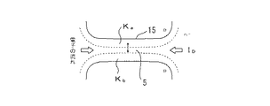
ガス分子が触媒層3に吸着して電気抵抗が変化すると、n型チャネル5の表面側のpn接合に印加される電圧が変化する。図2は、チャネル5の部分の拡大図である。上記のように、チャネル5の表面側および裏面側のpn接合15には、逆バイアス電圧が印加されているので、空乏層Ka,Kbがn型領域に張り出す。このため、電子の流れは、空乏層Ka,Kbによって、その間のn型領域に限定される。このうち、裏面側に形成される空乏層Kbは、触媒層を介在させず、直接、定電圧電源のマイナス電極が接続されているの、ガス吸着の有無にかかわらず一定の大きさを維持する。これに対して、表面側の空乏層Kaは、ガス吸着の量に応じて、pn接合15に印加される逆バイアス電圧が変化するので、ガス吸着量に応じて、その大きさが変化する。このため、ガス吸着量に応じて、n型チャネル5の断面積が変化して、電子の通りやすさが変化して、その結果、電流IDが変化する。電流IDの変化によって、ガス吸着量を知ることができる。検知対象のガス吸着量は、雰囲気中のそのガス濃度が低い場合には、雰囲気中の検知対象のガス濃度に比例する。よって、図3に示すように、電流IDの変化によって、検知対象のガス濃度を知ることができる。
When gas molecules are adsorbed on the catalyst layer 3 and the electric resistance changes, the voltage applied to the pn junction on the surface side of the n-
触媒層3は、粉末ペーストを圧着してp型領域6上に形成してもよいし、粉末ペーストをスクリーン印刷してもよい。また、スパッタリング法や、CVD(Chemical Vapor Deposition)法などの気相法によって蒸着してもよい。また、大量生産に適した真空蒸着法で蒸着することもできる。p型領域6、n側電極12およびp側電極11の製造などは、通常の半導体の処理装置、処理方法を用いて容易に行うことができる。
The catalyst layer 3 may be formed on the p-
図1に示すように、チャネル5はSiC基板1の表裏面に露出せず、p型領域6よりもSiC基板1の厚み中心側に位置する。このため、長期的に信頼性を保持することができる。また、表面の界面準位密度のばらつきの影響を受けないのでセンサ特性が安定しており、製造歩留りの低下を防止することができる。また、表面の界面準位の影響を受けないので、高い応答速度を得ることができる。
As shown in FIG. 1,
(本発明の実施の形態1の変形例)
図4は、本発明の実施の形態1のガスセンサ10の変形例を示す図である。裏面側のp側電極11bが、表面側と同様に、触媒層3を介在させてp型領域6に接続されている。この点が、図1に示すガスセンサ10と、相違している。裏面側においても、p側電極11bが、触媒層3を介在させてp型領域6に接続するため、チャネル5の裏面側に位置するpn接合15に形成される空乏層Kbの大きさは、裏面側の触媒層3におけるガス吸着量によって変化する。
(Modification of the first embodiment of the present invention)
FIG. 4 is a diagram showing a modification of the
図2では、空乏層Kbは固定されていて、チャネル5の断面積は、表面側の空乏層Kaにのみ依存していた。しかし、上記の変形によって空乏層Ka,Kbがともにガス吸着量の影響を受けて、大きさを変ずるので、ガス吸着によるチャネル5の断面積の変動を倍加することができる。したがって、感度を倍増することができる。また、上述の実施の形態1における利点は、そのまま、この変形例でも享受することができる。すなわち、チャネル5はSiC基板1の表裏面に露出せず、SiC基板の厚み中心付近に位置する。このため、長期的に信頼性を保持することができる。また、表面の界面準位密度のばらつきの影響を受けないのでセンサ特性が安定しており、製造歩留りの低下を防止することができる。また、表面の界面準位の影響を受けないので、高い応答速度を得ることができる。
In Figure 2, the depletion layer K b is fixed, the cross-sectional area of the
(実施の形態2)
図5は、本発明の実施の形態2におけるガスセンサ10を示す図である。このガスセンサ10では、感応層にイオン導電性酸素酸塩33を用いる点で、実施の形態1と相違する。イオン導電性酸素酸塩33は、検知対象のガスの分圧の変化に応じて酸素酸塩の電気化学的な解離平衡を生じ、それによって起電力変化が生じる。このため、表面側のp型領域6に、イオン導電性酸素酸塩33を介在させて、定電圧電源のマイナス電極を接続すると、pn接合15に印加される逆バイアス電圧が変化する。したがって、上述のように、空乏層Kaの大きさが変化してチャネル5の断面積が変化して、ドレイン電流IDの変化を生じる。この結果、ドレイン電流IDの変化によって対象ガスの濃度を検知することができる。実施の形態1では、対象のガスの吸着によって電気抵抗変化を生じ、これによってチャネル断面積の変化が生じた。これに対し、本実施の形態では、ガス分圧の変化に応じてイオン導電性酸素酸塩33の電気化学的な解離平衡が生じ、当該イオン導電性酸素酸塩33に起電力が生じて、pn接合15に印加される逆バイアス電圧が変化する。これによって、空乏層の張り出しの大きさの変化によるチャネル5の断面積の変化を利用する。したがって、感応層がイオン導電性酸素酸塩33であること以外の部分は、実施の形態1と同じであるので、説明はイオン導電性酸素酸塩に集中し、他の部分は省略する。
(Embodiment 2)
FIG. 5 is a diagram showing the
1.検知対象ガス
検知対象ガスは、二酸化炭素(CO2)、一酸化窒素(NO)、二酸化窒素(NO2)などを主対象とするが、そのほかのガスを対象とすることは問題なく可能である。たとえば、一酸化硫黄(SO)、二酸化硫黄(SO2)など可能である。
2.イオン導線性酸素酸塩
イオン導電性酸素酸塩は、当然であるが、検知対象ガスに応じて具体的な化合物は変わる。
1. Gas to be detected The gas to be detected is mainly carbon dioxide (CO 2 ), nitric oxide (NO), nitrogen dioxide (NO 2 ), etc., but other gases can be used without problems. . For example, sulfur monoxide (SO), sulfur dioxide (SO 2 ), and the like are possible.
2. Ion conductive oxyacid salt The ion conductive oxyacid salt is, of course, a specific compound depending on the gas to be detected.
(1)一酸化窒素(NO)、二酸化窒素(NO2)の場合
イオン導電性酸素酸塩には、金属亜硝酸酸塩、および/または金属硝酸塩を用いるのがよい。そして、増感剤として、白金(Pt)粒子を含むのが、感度を高める上で好ましい。
金属亜硝酸塩としては、たとえば、亜硝酸リチウム(LiNO2)、亜硝酸ナトリウム(NaNO2)、亜硝酸カリウム(KNO2)、亜硝酸ルビジウム(RbNO2)、亜硝酸セシウム(CsNO2)、亜硝酸バリウム(Ba(NO2)2)、亜硝酸ストロンチウム(Sr(NO2)2)などがある。これらの一種または二種以上から構成するのがよい。
また、金属硝酸塩としては、たとえば、硝酸リチウム(LiNO3)、硝酸ナトリウム(NaNO3)、硝酸カリウム(KNO3)、硝酸ルビジウム(RbNO2)、硝酸マグネシウム(Mg(NO3)2)、硝酸カルシウム(Ca(NO3)2)、硝酸ストロンチウム(Sr(NO3)2)、硝酸バリウム(Ba(NO3)2)、硝酸スカンジウム(Sc(NO3)3)、硝酸セリウム(Ce(NO3)3)、硝酸ジルコニウム(Zr(NO3)4)、硝酸鉄(Fe(NO3)2,Fe(NO3)3)、硝酸銅(Cu(NO3)2)、硝酸コバルト(Co(NO3)2)、硝酸スズ(Sn(NO3)4)、硝酸インジウム(In(NO3)3)、硝酸ニッケル(Ni(NO3)2)、硝酸鉛(Pb(NO3)2)、硝酸ビスマス(Bi(NO3)3)および希土類硝酸塩の、一種または二種以上から構成するのがよい。
(1) In the case of nitric oxide (NO) and nitrogen dioxide (NO 2 ) Metal nitrite and / or metal nitrate may be used as the ion conductive oxyacid salt. And it is preferable to include platinum (Pt) particles as a sensitizer in order to increase sensitivity.
Examples of the metal nitrite include lithium nitrite (LiNO 2 ), sodium nitrite (NaNO 2 ), potassium nitrite (KNO 2 ), rubidium nitrite (RbNO 2 ), cesium nitrite (CsNO 2 ), and barium nitrite. (Ba (NO 2 ) 2 ), strontium nitrite (Sr (NO 2 ) 2 ), and the like. It is good to comprise from 1 type, or 2 or more types of these.
Examples of the metal nitrate include lithium nitrate (LiNO 3 ), sodium nitrate (NaNO 3 ), potassium nitrate (KNO 3 ), rubidium nitrate (RbNO 2 ), magnesium nitrate (Mg (NO 3 ) 2 ), calcium nitrate ( Ca (NO 3 ) 2 ), strontium nitrate (Sr (NO 3 ) 2 ), barium nitrate (Ba (NO 3 ) 2 ), scandium nitrate (Sc (NO 3 ) 3 ), cerium nitrate (Ce (NO 3 ) 3 ), Zirconium nitrate (Zr (NO 3 ) 4 ), iron nitrate (Fe (NO 3 ) 2 , Fe (NO 3 ) 3 ), copper nitrate (Cu (NO 3 ) 2 ), cobalt nitrate (Co (NO 3 )) 2 ), tin nitrate (Sn (NO 3 ) 4 ), indium nitrate (In (NO 3 ) 3 ), nickel nitrate (Ni (NO 3 ) 2 ), lead nitrate ( Pb (NO 3 ) 2 ), bismuth nitrate (Bi (NO 3 ) 3 ), and rare earth nitrates may be used alone or in combination.
(2)二酸化炭素(CO2)
イオン導電性酸素酸塩には、金属炭酸塩、および/または金属炭酸水素塩を用いる。
金属炭酸塩としては、たとえば、炭酸リチウム(Li2CO3)、炭酸ナトリウム(Na2CO3)、炭酸カリウム(K2CO3)、炭酸ルビジウム(Rb2CO3)、炭酸セシウム(Cs2CO3)、炭酸マグネシウム(Mg(CO3)2)、炭酸カルシウム(CaCO3)、炭酸ストロンチウム(SrCO3)、炭酸バリウム(BaCO3)、炭酸鉄(FeCO3)、炭酸銅(Cu2CO3)、炭酸ニッケル(NiCO3)、炭酸鉛(PbCO3)、炭酸マンガン(MnCO3)、炭酸カドミウム(CdCO3)、炭酸銀(Ag2CO3)、炭酸コバルト(CoCO3)および希土類硝酸塩の、一種または二種以上から構成するのがよい。
金属炭素水素塩としては、たとえば、炭酸水素ナトリウム(NaHCO3)、炭酸水素カリウム(KHCO3)、炭酸水素ルビジウム(RbHCO3)、炭酸水素セシウム(CsHCO3)の一種または二種以上から構成するのがよい。
(2) Carbon dioxide (CO 2 )
As the ion conductive oxyacid salt, a metal carbonate and / or a metal hydrogen carbonate is used.
Examples of the metal carbonate include lithium carbonate (Li 2 CO 3 ), sodium carbonate (Na 2 CO 3 ), potassium carbonate (K 2 CO 3 ), rubidium carbonate (Rb 2 CO 3 ), and cesium carbonate (Cs 2 CO). 3 ), magnesium carbonate (Mg (CO 3 ) 2 ), calcium carbonate (CaCO 3 ), strontium carbonate (SrCO 3 ), barium carbonate (BaCO 3 ), iron carbonate (FeCO 3 ), copper carbonate (Cu 2 CO 3 ) , nickel carbonate (NiCO 3), lead carbonate (PbCO 3), manganese carbonate (MnCO 3), cadmium carbonate (CdCO 3), silver carbonate (Ag 2 CO 3), of cobalt carbonate (CoCO 3) and rare earth nitrates, one Or it is good to comprise from 2 or more types.
As the metal carbon hydrogen salt may, for example, sodium bicarbonate (NaHCO 3), potassium bicarbonate (KHCO 3), bicarbonate rubidium (RbHCO 3), to consist of one or two or more of cesium hydrogencarbonate (CsHCO 3) Is good.
3.イオン導電性酸素酸塩の配置
イオン導電性酸素酸塩33は、粉末ペースト状にしたものを圧着して配置することができる。また、粉末ペーストをスクリーン印刷して配置してもよい。さらに、粉末ペーストを加熱溶融圧着によって接合してもよい。また、薄膜として、スパッタリング法やCVD法で形成してもよい。真空蒸着法で蒸着してもよい。
3. Arrangement of ion conductive oxyacid salt The ion
上記のイオン導電性酸素酸塩33は、検知対象のガス選択性を向上させることができる。また、チャネル5が半導体基板の厚み中心付近に形成される点では、実施の形態1と同じである。このため、長期的に信頼性を保持することができる。また、表面の界面準位密度のばらつきの影響を受けないのでセンサ特性が安定しており、製造歩留りの低下を防止することができる。また、表面の界面準位の影響を受けないので、高い応答速度を得ることができる。
The ion
(本発明の実施の形態2の変形例)
図6は、本発明の実施の形態2の変形例におけるガスセンサ10の感応層の部分の拡大図である。他の部分は、図5に示すガスセンサ10と同じである。図6に示す変形例のガスセンサ10では、感応層に、(イオン導電性酸素酸塩33/固体電解質34)を用いている点で、図5に示すガスセンサの感応層の内容と相違する。すなわち、チャネル5の表面側のp型領域6に接して、固体電解質34が配置され、その上にイオン導電性酸素酸塩33が配置される。
(Modification of Embodiment 2 of the present invention)
FIG. 6 is an enlarged view of a portion of the sensitive layer of the
固体電解質34とイオン導電性酸素酸塩33とを組み合わせた利点は、より低濃度の対象ガスを検知できる点にある。その理由は、固体電解質34によって、イオン導電性酸素酸塩33と固体電解質34との間にイオンブリッジが形成され、大きな化学ポテンシャルが形成されるためと考えられる。チャネル5が、半導体基板1の厚み中心付近に形成される構造は、不変である。このため、長期的に信頼性を保持することができる。また、表面の界面準位密度のばらつきの影響を受けないのでセンサ特性が安定しており、製造歩留りの低下を防止することができる。また、表面の界面準位の影響を受けないので、高い応答速度を得ることができる。
The advantage of combining the
(実施の形態3)
図7は、本発明の実施の形態3におけるガスセンサ10を示す図である。本実施の形態では、感応層には、上述したものに比べてとくに新しいことはない。図7に示すガスセンサ10の場合には、触媒3を用いている。この触媒3の代わりに、イオン導電性酸素酸塩33、または(イオン導電性酸素酸塩33/固体電解質34)を用いてもよい。本実施の形態における特徴は、電流IDが半導体基板1の厚み方向に沿って流れる点にある。図7に示すガスセンサ10では、チャネル5は、半導体基板1を貫通するように設けられる。このチャネル5の断面積を変化させるために、pn接合15に逆バイアス電圧が印加される。
(Embodiment 3)
FIG. 7 is a diagram showing the
n型チャネル5を取り囲むように位置するp型領域6には、触媒層3を介在させてp側電極11a,11bが接続される。図7では、平面形状が矩形の半導体基板に対して、相対向する2つのp型領域6が設けられ、その2つのp型領域にp側電極が1つずつ設けられている。また、チャネル5を含む残りのn型領域には、表面にn側電極12aが、また裏面にn側電極12bが接続されている。したがって、n側電極12a,12bと、p側電極11a,11bとの間に、触媒3を介在させて、定電圧電源9から電圧(pn接合15に対する逆バイアス電圧)が印加される。
P-
ソース電極21は表面側のn型領域に接続され、ドレイン電極22は裏面側のn型領域に接続され、チャネル5によって連絡されている。チャネル5には、ドレイン電圧VDによって電流IDが流れる。しかし、図8に示すように、ガスが触媒3に吸着されると、上述のように、空乏層Ka,Kbの大きさが変化することによって、電流IDが変化する。これによって、電流IDの変化によって、雰囲気中のガスの濃度を検知することができる。
The
図7に示すガスセンサ10は、通常の半導体の処理装置および処理方法を用いて、簡単に製造することができる。また、n側電極12a,12bは、表面と裏面とに1つずつ、合計2つ設けたが、表面または裏面に、全部で1つだけ設けてもよい。さらに、p側電極11a,11bについても、全部で1つでもよい。空乏層は、片側だけ生成しただけでもチャネル5の断面積を変化させることができ、ガス吸着量の多寡を検知できるからである。
The
チャネル5は、半導体基板1の厚み方向に貫通するように形成されるので、チャネルの主要部が半導体基板の中心付近に形成される構造は、不変である。このため、長期的に信頼性を保持することができる。また、表面の界面準位密度のばらつきの影響を受けないのでセンサ特性が安定しており、製造歩留りの低下を防止することができる。また、表面の界面準位の影響を受けないので、高い応答速度を得ることができる。さらに、半導体基板1の厚みは4μm程度なので、ガス検知の応答速度を、半導体基板の板面に沿って電流IDが流れる場合よりも、大きくすることができる。
Since the
上記において、本発明の実施の形態について説明を行ったが、上記に開示された本発明の実施の形態は、あくまで例示であって、本発明の範囲はこれら発明の実施の形態に限定されない。本発明の範囲は、特許請求の範囲の記載によって示され、さらに特許請求の範囲の記載と均等の意味および範囲内でのすべての変更を含むものである。 Although the embodiments of the present invention have been described above, the embodiments of the present invention disclosed above are merely examples, and the scope of the present invention is not limited to these embodiments. The scope of the present invention is indicated by the description of the scope of claims, and further includes meanings equivalent to the description of the scope of claims and all modifications within the scope.
本発明によれば、性能が長期間安定して維持され、特性が安定しており、応答速度が大きいガスセンサを得ることができ、耐熱性の高いSiCなどの半導体を用いることによって、排気ガス規制、燃費向上に資することが期待される。 According to the present invention, it is possible to obtain a gas sensor whose performance is stably maintained for a long period of time, whose characteristics are stable, and whose response speed is large, and by using a semiconductor such as SiC having high heat resistance, exhaust gas regulation is achieved. It is expected to contribute to improved fuel economy.
1 半導体基板(SiC基板)、3 ガス感応層(触媒(酸化物半導体))、5 n型チャネル、6 p型領域、9 定電圧電源(電池)、10 ガスセンサ、11a,11b p側電極、12,12a,12b n側電極、15 pn接合、21 ソース電極、22 ドレイン電極、31 電流計、33 ガス感応層(イオン導電性酸素酸塩)、34 固体電解質、D ドレイン電極、ID ドレイン電流、Ka,Kb 空乏層、S ソース電極、VD ドレイン電圧。
DESCRIPTION OF
Claims (5)
前記第1導電型半導体基板の表面から内部へと設けられた第2導電型領域と、
前記第2導電型領域の表面に電気的に接続されたガス感応層と、
前記ガス感応層の上に位置して電気的に接続された第2導電側電極と、
前記第2導電型領域を挟むように、前記表面に設けられた、ソース電極およびドレイン電極と、
前記半導体基板の中で前記第2導電側領域に接し、前記ソース電極とドレイン電極とを連絡する、第1導電型の通路と、
前記第1導電型の通路に連絡している表面または裏面に電気的に接続された第1導電側電極とを備え、
前記ガス感応層を介在させて、前記第1導電側電極と第2導電側電極との間に電圧を加えて、前記第2導電側領域と第1導電型の通路とのpn接合に逆バイアス電圧を印加することを特徴とする、ガスセンサ。 A first conductivity type semiconductor substrate;
A second conductivity type region provided from the surface to the inside of the first conductivity type semiconductor substrate;
A gas sensitive layer electrically connected to the surface of the second conductivity type region;
A second conductive side electrode located on and electrically connected to the gas sensitive layer;
A source electrode and a drain electrode provided on the surface so as to sandwich the second conductivity type region;
A first conductivity type path in contact with the second conductive side region in the semiconductor substrate and connecting the source electrode and the drain electrode;
A first conductive side electrode electrically connected to a front surface or a back surface communicating with the first conductivity type passage;
A voltage is applied between the first conductive side electrode and the second conductive side electrode through the gas sensitive layer, and a reverse bias is applied to the pn junction between the second conductive side region and the first conductive type passage. A gas sensor, wherein a voltage is applied.
前記半導体基板の、表面に位置するソース電極、および裏面に位置するドレイン電極と、
前記ソース電極とドレイン電極とを連絡している第1導電型の通路を、取り囲むように設けられ、表面または裏面に露出する第2導電型領域と、
前記露出した第2導電型領域に電気的に接続されたガス感応層と、
前記ガス感応層の上に位置して電気的に接続された第2導電側電極と、
前記第1導電型の通路に連絡している表面または裏面に電気的に接続された第1導電側電極とを備え、
前記ガス感応層を介在させて、前記第1導電側電極と第2導電側電極との間に電圧を加えて、前記第1導電側領域の通路の周りのpn接合に逆バイアス電圧を印加することを特徴とする、ガスセンサ。 A first conductivity type semiconductor substrate;
A source electrode located on the front surface and a drain electrode located on the back surface of the semiconductor substrate;
A second conductivity type region which is provided so as to surround the first conductivity type passage connecting the source electrode and the drain electrode, and is exposed on the front surface or the back surface;
A gas sensitive layer electrically connected to the exposed second conductivity type region;
A second conductive side electrode located on and electrically connected to the gas sensitive layer;
A first conductive side electrode electrically connected to a front surface or a back surface communicating with the first conductivity type passage;
A voltage is applied between the first conductive side electrode and the second conductive side electrode with the gas sensitive layer interposed, and a reverse bias voltage is applied to the pn junction around the passage of the first conductive side region. A gas sensor.
The gas sensor according to claim 1, wherein the sensitive layer is porous.
Priority Applications (1)
| Application Number | Priority Date | Filing Date | Title |
|---|---|---|---|
| JP2008177498A JP5168725B2 (en) | 2008-07-08 | 2008-07-08 | Gas sensor |
Applications Claiming Priority (1)
| Application Number | Priority Date | Filing Date | Title |
|---|---|---|---|
| JP2008177498A JP5168725B2 (en) | 2008-07-08 | 2008-07-08 | Gas sensor |
Publications (2)
| Publication Number | Publication Date |
|---|---|
| JP2010019555A true JP2010019555A (en) | 2010-01-28 |
| JP5168725B2 JP5168725B2 (en) | 2013-03-27 |
Family
ID=41704634
Family Applications (1)
| Application Number | Title | Priority Date | Filing Date |
|---|---|---|---|
| JP2008177498A Expired - Fee Related JP5168725B2 (en) | 2008-07-08 | 2008-07-08 | Gas sensor |
Country Status (1)
| Country | Link |
|---|---|
| JP (1) | JP5168725B2 (en) |
Cited By (3)
| Publication number | Priority date | Publication date | Assignee | Title |
|---|---|---|---|---|
| JP2011226800A (en) * | 2010-04-15 | 2011-11-10 | Hokkaido Univ | Sensor and method of manufacturing the same |
| JP2012159511A (en) * | 2011-02-02 | 2012-08-23 | Robert Bosch Gmbh | Method and monitoring device for monitoring at least one function of chemical sensitive field effect transistor |
| JP2014013239A (en) * | 2012-07-03 | 2014-01-23 | Robert Bosch Gmbh | Gas sensor, and method of manufacturing the same |
Citations (6)
| Publication number | Priority date | Publication date | Assignee | Title |
|---|---|---|---|---|
| JPS63101740A (en) * | 1986-10-17 | 1988-05-06 | Nippon Telegr & Teleph Corp <Ntt> | Vertical fet type gas sensor |
| JPS63265157A (en) * | 1987-04-23 | 1988-11-01 | Matsushita Electric Works Ltd | Ion sensor |
| JPH01263550A (en) * | 1988-04-14 | 1989-10-20 | Terumo Corp | Ion sensor |
| JPH02249962A (en) * | 1989-03-23 | 1990-10-05 | Terumo Corp | Fet sensor |
| JPH0843334A (en) * | 1994-07-28 | 1996-02-16 | Nec Corp | Measuring method for impurity in semiconductor board |
| JP2003043010A (en) * | 2001-04-25 | 2003-02-13 | Nikon Corp | Element, device, and method for detecting organic molecule |
-
2008
- 2008-07-08 JP JP2008177498A patent/JP5168725B2/en not_active Expired - Fee Related
Patent Citations (6)
| Publication number | Priority date | Publication date | Assignee | Title |
|---|---|---|---|---|
| JPS63101740A (en) * | 1986-10-17 | 1988-05-06 | Nippon Telegr & Teleph Corp <Ntt> | Vertical fet type gas sensor |
| JPS63265157A (en) * | 1987-04-23 | 1988-11-01 | Matsushita Electric Works Ltd | Ion sensor |
| JPH01263550A (en) * | 1988-04-14 | 1989-10-20 | Terumo Corp | Ion sensor |
| JPH02249962A (en) * | 1989-03-23 | 1990-10-05 | Terumo Corp | Fet sensor |
| JPH0843334A (en) * | 1994-07-28 | 1996-02-16 | Nec Corp | Measuring method for impurity in semiconductor board |
| JP2003043010A (en) * | 2001-04-25 | 2003-02-13 | Nikon Corp | Element, device, and method for detecting organic molecule |
Cited By (3)
| Publication number | Priority date | Publication date | Assignee | Title |
|---|---|---|---|---|
| JP2011226800A (en) * | 2010-04-15 | 2011-11-10 | Hokkaido Univ | Sensor and method of manufacturing the same |
| JP2012159511A (en) * | 2011-02-02 | 2012-08-23 | Robert Bosch Gmbh | Method and monitoring device for monitoring at least one function of chemical sensitive field effect transistor |
| JP2014013239A (en) * | 2012-07-03 | 2014-01-23 | Robert Bosch Gmbh | Gas sensor, and method of manufacturing the same |
Also Published As
| Publication number | Publication date |
|---|---|
| JP5168725B2 (en) | 2013-03-27 |
Similar Documents
| Publication | Publication Date | Title |
|---|---|---|
| Sharma et al. | Recent advances on H2 sensor technologies based on MOX and FET devices: A review | |
| JP4418672B2 (en) | Solid electrochemical cell for measuring the concentration of a component in a gas mixture | |
| US9952175B2 (en) | Gas sensor and sensor device | |
| KR20170067775A (en) | AMPEROMETRIC SOLID ELECTROLYTE SENSOR AND METHOD FOR DETECTING NH3 AND NOx | |
| KR101052618B1 (en) | Nitrogen oxide gas sensor with long term signal stability | |
| EP3786627B1 (en) | Mems type semiconductor gas detection element | |
| JPH09274011A (en) | Nitrogen oxide detector | |
| KR102009059B1 (en) | Sensor and method for manufacturing a sensor | |
| JP5168725B2 (en) | Gas sensor | |
| JP6941373B2 (en) | Amperometric electrochemical sensors, sensor systems and detection methods | |
| KR101052617B1 (en) | Nitrogen Oxide Gas Sensor | |
| JP3845741B2 (en) | Nitrogen oxide detection method and sensor element for nitrogen oxide detection | |
| US11761923B2 (en) | Amperometric electrochemical sensors, sensor systems and detection methods | |
| WO2016125283A1 (en) | Gas sensor and sensor device | |
| JP2000512384A (en) | Gas sensor | |
| US20190317036A1 (en) | Gas sensor | |
| KR20100036726A (en) | Nox gas sensor having | |
| JP4340639B2 (en) | Hydrogen sensor and hydrogen detection method | |
| JP4467022B2 (en) | Gas sensor | |
| KR101133267B1 (en) | NOx gas sensor | |
| JP2001221763A (en) | Nitrogen oxide gas sensor | |
| KR20180059578A (en) | Gas sensor for measuring different gases, and corresponding production method | |
| KR101455059B1 (en) | Nitrogen oxide gas sensor and method for measuring nitrogen oxide gas using the same | |
| Bi et al. | Solid-state amperometric CH4 sensor using, LaGaO3-based electrolyte | |
| JP6806100B2 (en) | Gas sensor |
Legal Events
| Date | Code | Title | Description |
|---|---|---|---|
| A621 | Written request for application examination |
Free format text: JAPANESE INTERMEDIATE CODE: A621 Effective date: 20110616 |
|
| A977 | Report on retrieval |
Free format text: JAPANESE INTERMEDIATE CODE: A971007 Effective date: 20120920 |
|
| A01 | Written decision to grant a patent or to grant a registration (utility model) |
Free format text: JAPANESE INTERMEDIATE CODE: A01 Effective date: 20121203 |
|
| A61 | First payment of annual fees (during grant procedure) |
Free format text: JAPANESE INTERMEDIATE CODE: A61 Effective date: 20121216 |
|
| LAPS | Cancellation because of no payment of annual fees |