JP2010012774A - Inkjet recording head and its manufacturing method - Google Patents
Inkjet recording head and its manufacturing method Download PDFInfo
- Publication number
- JP2010012774A JP2010012774A JP2009113565A JP2009113565A JP2010012774A JP 2010012774 A JP2010012774 A JP 2010012774A JP 2009113565 A JP2009113565 A JP 2009113565A JP 2009113565 A JP2009113565 A JP 2009113565A JP 2010012774 A JP2010012774 A JP 2010012774A
- Authority
- JP
- Japan
- Prior art keywords
- recording element
- element substrate
- arrangement
- recording head
- adhesive
- Prior art date
- Legal status (The legal status is an assumption and is not a legal conclusion. Google has not performed a legal analysis and makes no representation as to the accuracy of the status listed.)
- Granted
Links
- 238000004519 manufacturing process Methods 0.000 title claims abstract description 13
- 239000000758 substrate Substances 0.000 claims abstract description 130
- 239000000853 adhesive Substances 0.000 claims abstract description 55
- 230000001070 adhesive effect Effects 0.000 claims abstract description 55
- 238000000034 method Methods 0.000 claims description 23
- 238000007599 discharging Methods 0.000 claims description 3
- 238000010438 heat treatment Methods 0.000 claims description 2
- 230000001678 irradiating effect Effects 0.000 claims 1
- 229920001187 thermosetting polymer Polymers 0.000 abstract description 33
- 239000012790 adhesive layer Substances 0.000 description 7
- 238000006243 chemical reaction Methods 0.000 description 6
- 238000001723 curing Methods 0.000 description 6
- 238000010586 diagram Methods 0.000 description 4
- 239000012778 molding material Substances 0.000 description 3
- 230000000694 effects Effects 0.000 description 2
- 238000009429 electrical wiring Methods 0.000 description 2
- 238000003754 machining Methods 0.000 description 2
- 229920001955 polyphenylene ether Polymers 0.000 description 2
- 239000003795 chemical substances by application Substances 0.000 description 1
- 239000013078 crystal Substances 0.000 description 1
- 238000005520 cutting process Methods 0.000 description 1
- 238000005516 engineering process Methods 0.000 description 1
- 238000005530 etching Methods 0.000 description 1
- 238000007667 floating Methods 0.000 description 1
- 238000013007 heat curing Methods 0.000 description 1
- 238000000465 moulding Methods 0.000 description 1
- 238000000206 photolithography Methods 0.000 description 1
- 230000000704 physical effect Effects 0.000 description 1
- 238000005488 sandblasting Methods 0.000 description 1
- 239000000565 sealant Substances 0.000 description 1
- 238000007789 sealing Methods 0.000 description 1
Images


Classifications
-
- B—PERFORMING OPERATIONS; TRANSPORTING
- B41—PRINTING; LINING MACHINES; TYPEWRITERS; STAMPS
- B41J—TYPEWRITERS; SELECTIVE PRINTING MECHANISMS, i.e. MECHANISMS PRINTING OTHERWISE THAN FROM A FORME; CORRECTION OF TYPOGRAPHICAL ERRORS
- B41J2/00—Typewriters or selective printing mechanisms characterised by the printing or marking process for which they are designed
- B41J2/005—Typewriters or selective printing mechanisms characterised by the printing or marking process for which they are designed characterised by bringing liquid or particles selectively into contact with a printing material
- B41J2/01—Ink jet
- B41J2/135—Nozzles
- B41J2/16—Production of nozzles
- B41J2/1621—Manufacturing processes
- B41J2/1623—Manufacturing processes bonding and adhesion
-
- B—PERFORMING OPERATIONS; TRANSPORTING
- B29—WORKING OF PLASTICS; WORKING OF SUBSTANCES IN A PLASTIC STATE IN GENERAL
- B29C—SHAPING OR JOINING OF PLASTICS; SHAPING OF MATERIAL IN A PLASTIC STATE, NOT OTHERWISE PROVIDED FOR; AFTER-TREATMENT OF THE SHAPED PRODUCTS, e.g. REPAIRING
- B29C35/00—Heating, cooling or curing, e.g. crosslinking or vulcanising; Apparatus therefor
- B29C35/02—Heating or curing, e.g. crosslinking or vulcanizing during moulding, e.g. in a mould
- B29C35/08—Heating or curing, e.g. crosslinking or vulcanizing during moulding, e.g. in a mould by wave energy or particle radiation
- B29C35/0805—Heating or curing, e.g. crosslinking or vulcanizing during moulding, e.g. in a mould by wave energy or particle radiation using electromagnetic radiation
- B29C2035/0827—Heating or curing, e.g. crosslinking or vulcanizing during moulding, e.g. in a mould by wave energy or particle radiation using electromagnetic radiation using UV radiation
-
- B—PERFORMING OPERATIONS; TRANSPORTING
- B29—WORKING OF PLASTICS; WORKING OF SUBSTANCES IN A PLASTIC STATE IN GENERAL
- B29C—SHAPING OR JOINING OF PLASTICS; SHAPING OF MATERIAL IN A PLASTIC STATE, NOT OTHERWISE PROVIDED FOR; AFTER-TREATMENT OF THE SHAPED PRODUCTS, e.g. REPAIRING
- B29C65/00—Joining or sealing of preformed parts, e.g. welding of plastics materials; Apparatus therefor
- B29C65/02—Joining or sealing of preformed parts, e.g. welding of plastics materials; Apparatus therefor by heating, with or without pressure
- B29C65/14—Joining or sealing of preformed parts, e.g. welding of plastics materials; Apparatus therefor by heating, with or without pressure using wave energy, i.e. electromagnetic radiation, or particle radiation
- B29C65/1403—Joining or sealing of preformed parts, e.g. welding of plastics materials; Apparatus therefor by heating, with or without pressure using wave energy, i.e. electromagnetic radiation, or particle radiation characterised by the type of electromagnetic or particle radiation
- B29C65/1406—Ultraviolet [UV] radiation
-
- B—PERFORMING OPERATIONS; TRANSPORTING
- B29—WORKING OF PLASTICS; WORKING OF SUBSTANCES IN A PLASTIC STATE IN GENERAL
- B29C—SHAPING OR JOINING OF PLASTICS; SHAPING OF MATERIAL IN A PLASTIC STATE, NOT OTHERWISE PROVIDED FOR; AFTER-TREATMENT OF THE SHAPED PRODUCTS, e.g. REPAIRING
- B29C65/00—Joining or sealing of preformed parts, e.g. welding of plastics materials; Apparatus therefor
- B29C65/02—Joining or sealing of preformed parts, e.g. welding of plastics materials; Apparatus therefor by heating, with or without pressure
- B29C65/14—Joining or sealing of preformed parts, e.g. welding of plastics materials; Apparatus therefor by heating, with or without pressure using wave energy, i.e. electromagnetic radiation, or particle radiation
- B29C65/1403—Joining or sealing of preformed parts, e.g. welding of plastics materials; Apparatus therefor by heating, with or without pressure using wave energy, i.e. electromagnetic radiation, or particle radiation characterised by the type of electromagnetic or particle radiation
- B29C65/1412—Infrared [IR] radiation
-
- B—PERFORMING OPERATIONS; TRANSPORTING
- B29—WORKING OF PLASTICS; WORKING OF SUBSTANCES IN A PLASTIC STATE IN GENERAL
- B29C—SHAPING OR JOINING OF PLASTICS; SHAPING OF MATERIAL IN A PLASTIC STATE, NOT OTHERWISE PROVIDED FOR; AFTER-TREATMENT OF THE SHAPED PRODUCTS, e.g. REPAIRING
- B29C65/00—Joining or sealing of preformed parts, e.g. welding of plastics materials; Apparatus therefor
- B29C65/48—Joining or sealing of preformed parts, e.g. welding of plastics materials; Apparatus therefor using adhesives, i.e. using supplementary joining material; solvent bonding
- B29C65/4805—Joining or sealing of preformed parts, e.g. welding of plastics materials; Apparatus therefor using adhesives, i.e. using supplementary joining material; solvent bonding characterised by the type of adhesives
- B29C65/483—Reactive adhesives, e.g. chemically curing adhesives
- B29C65/4835—Heat curing adhesives
-
- B—PERFORMING OPERATIONS; TRANSPORTING
- B29—WORKING OF PLASTICS; WORKING OF SUBSTANCES IN A PLASTIC STATE IN GENERAL
- B29C—SHAPING OR JOINING OF PLASTICS; SHAPING OF MATERIAL IN A PLASTIC STATE, NOT OTHERWISE PROVIDED FOR; AFTER-TREATMENT OF THE SHAPED PRODUCTS, e.g. REPAIRING
- B29C65/00—Joining or sealing of preformed parts, e.g. welding of plastics materials; Apparatus therefor
- B29C65/48—Joining or sealing of preformed parts, e.g. welding of plastics materials; Apparatus therefor using adhesives, i.e. using supplementary joining material; solvent bonding
- B29C65/50—Joining or sealing of preformed parts, e.g. welding of plastics materials; Apparatus therefor using adhesives, i.e. using supplementary joining material; solvent bonding using adhesive tape, e.g. thermoplastic tape; using threads or the like
- B29C65/5057—Joining or sealing of preformed parts, e.g. welding of plastics materials; Apparatus therefor using adhesives, i.e. using supplementary joining material; solvent bonding using adhesive tape, e.g. thermoplastic tape; using threads or the like positioned between the surfaces to be joined
-
- B—PERFORMING OPERATIONS; TRANSPORTING
- B29—WORKING OF PLASTICS; WORKING OF SUBSTANCES IN A PLASTIC STATE IN GENERAL
- B29C—SHAPING OR JOINING OF PLASTICS; SHAPING OF MATERIAL IN A PLASTIC STATE, NOT OTHERWISE PROVIDED FOR; AFTER-TREATMENT OF THE SHAPED PRODUCTS, e.g. REPAIRING
- B29C66/00—General aspects of processes or apparatus for joining preformed parts
- B29C66/50—General aspects of joining tubular articles; General aspects of joining long products, i.e. bars or profiled elements; General aspects of joining single elements to tubular articles, hollow articles or bars; General aspects of joining several hollow-preforms to form hollow or tubular articles
- B29C66/51—Joining tubular articles, profiled elements or bars; Joining single elements to tubular articles, hollow articles or bars; Joining several hollow-preforms to form hollow or tubular articles
- B29C66/53—Joining single elements to tubular articles, hollow articles or bars
- B29C66/534—Joining single elements to open ends of tubular or hollow articles or to the ends of bars
- B29C66/5346—Joining single elements to open ends of tubular or hollow articles or to the ends of bars said single elements being substantially flat
- B29C66/53461—Joining single elements to open ends of tubular or hollow articles or to the ends of bars said single elements being substantially flat joining substantially flat covers and/or substantially flat bottoms to open ends of container bodies
-
- B—PERFORMING OPERATIONS; TRANSPORTING
- B29—WORKING OF PLASTICS; WORKING OF SUBSTANCES IN A PLASTIC STATE IN GENERAL
- B29C—SHAPING OR JOINING OF PLASTICS; SHAPING OF MATERIAL IN A PLASTIC STATE, NOT OTHERWISE PROVIDED FOR; AFTER-TREATMENT OF THE SHAPED PRODUCTS, e.g. REPAIRING
- B29C66/00—General aspects of processes or apparatus for joining preformed parts
- B29C66/90—Measuring or controlling the joining process
- B29C66/96—Measuring or controlling the joining process characterised by the method for implementing the controlling of the joining process
- B29C66/967—Measuring or controlling the joining process characterised by the method for implementing the controlling of the joining process involving special data inputs or special data outputs, e.g. for monitoring purposes
- B29C66/9672—Measuring or controlling the joining process characterised by the method for implementing the controlling of the joining process involving special data inputs or special data outputs, e.g. for monitoring purposes involving special data inputs, e.g. involving barcodes, RFID tags
-
- B—PERFORMING OPERATIONS; TRANSPORTING
- B29—WORKING OF PLASTICS; WORKING OF SUBSTANCES IN A PLASTIC STATE IN GENERAL
- B29K—INDEXING SCHEME ASSOCIATED WITH SUBCLASSES B29B, B29C OR B29D, RELATING TO MOULDING MATERIALS OR TO MATERIALS FOR MOULDS, REINFORCEMENTS, FILLERS OR PREFORMED PARTS, e.g. INSERTS
- B29K2083/00—Use of polymers having silicon, with or without sulfur, nitrogen, oxygen, or carbon only, in the main chain, as moulding material
-
- B—PERFORMING OPERATIONS; TRANSPORTING
- B29—WORKING OF PLASTICS; WORKING OF SUBSTANCES IN A PLASTIC STATE IN GENERAL
- B29L—INDEXING SCHEME ASSOCIATED WITH SUBCLASS B29C, RELATING TO PARTICULAR ARTICLES
- B29L2031/00—Other particular articles
- B29L2031/767—Printing equipment or accessories therefor
-
- B—PERFORMING OPERATIONS; TRANSPORTING
- B41—PRINTING; LINING MACHINES; TYPEWRITERS; STAMPS
- B41J—TYPEWRITERS; SELECTIVE PRINTING MECHANISMS, i.e. MECHANISMS PRINTING OTHERWISE THAN FROM A FORME; CORRECTION OF TYPOGRAPHICAL ERRORS
- B41J2/00—Typewriters or selective printing mechanisms characterised by the printing or marking process for which they are designed
- B41J2/005—Typewriters or selective printing mechanisms characterised by the printing or marking process for which they are designed characterised by bringing liquid or particles selectively into contact with a printing material
- B41J2/01—Ink jet
- B41J2/135—Nozzles
- B41J2/14—Structure thereof only for on-demand ink jet heads
- B41J2002/14362—Assembling elements of heads
-
- B—PERFORMING OPERATIONS; TRANSPORTING
- B41—PRINTING; LINING MACHINES; TYPEWRITERS; STAMPS
- B41J—TYPEWRITERS; SELECTIVE PRINTING MECHANISMS, i.e. MECHANISMS PRINTING OTHERWISE THAN FROM A FORME; CORRECTION OF TYPOGRAPHICAL ERRORS
- B41J2202/00—Embodiments of or processes related to ink-jet or thermal heads
- B41J2202/01—Embodiments of or processes related to ink-jet heads
- B41J2202/22—Manufacturing print heads
-
- Y—GENERAL TAGGING OF NEW TECHNOLOGICAL DEVELOPMENTS; GENERAL TAGGING OF CROSS-SECTIONAL TECHNOLOGIES SPANNING OVER SEVERAL SECTIONS OF THE IPC; TECHNICAL SUBJECTS COVERED BY FORMER USPC CROSS-REFERENCE ART COLLECTIONS [XRACs] AND DIGESTS
- Y10—TECHNICAL SUBJECTS COVERED BY FORMER USPC
- Y10T—TECHNICAL SUBJECTS COVERED BY FORMER US CLASSIFICATION
- Y10T156/00—Adhesive bonding and miscellaneous chemical manufacture
- Y10T156/10—Methods of surface bonding and/or assembly therefor
-
- Y—GENERAL TAGGING OF NEW TECHNOLOGICAL DEVELOPMENTS; GENERAL TAGGING OF CROSS-SECTIONAL TECHNOLOGIES SPANNING OVER SEVERAL SECTIONS OF THE IPC; TECHNICAL SUBJECTS COVERED BY FORMER USPC CROSS-REFERENCE ART COLLECTIONS [XRACs] AND DIGESTS
- Y10—TECHNICAL SUBJECTS COVERED BY FORMER USPC
- Y10T—TECHNICAL SUBJECTS COVERED BY FORMER US CLASSIFICATION
- Y10T29/00—Metal working
- Y10T29/49—Method of mechanical manufacture
- Y10T29/49002—Electrical device making
- Y10T29/49082—Resistor making
- Y10T29/49083—Heater type
-
- Y—GENERAL TAGGING OF NEW TECHNOLOGICAL DEVELOPMENTS; GENERAL TAGGING OF CROSS-SECTIONAL TECHNOLOGIES SPANNING OVER SEVERAL SECTIONS OF THE IPC; TECHNICAL SUBJECTS COVERED BY FORMER USPC CROSS-REFERENCE ART COLLECTIONS [XRACs] AND DIGESTS
- Y10—TECHNICAL SUBJECTS COVERED BY FORMER USPC
- Y10T—TECHNICAL SUBJECTS COVERED BY FORMER US CLASSIFICATION
- Y10T29/00—Metal working
- Y10T29/49—Method of mechanical manufacture
- Y10T29/49002—Electrical device making
- Y10T29/49117—Conductor or circuit manufacturing
- Y10T29/49124—On flat or curved insulated base, e.g., printed circuit, etc.
- Y10T29/4913—Assembling to base an electrical component, e.g., capacitor, etc.
- Y10T29/49133—Assembling to base an electrical component, e.g., capacitor, etc. with component orienting
-
- Y—GENERAL TAGGING OF NEW TECHNOLOGICAL DEVELOPMENTS; GENERAL TAGGING OF CROSS-SECTIONAL TECHNOLOGIES SPANNING OVER SEVERAL SECTIONS OF THE IPC; TECHNICAL SUBJECTS COVERED BY FORMER USPC CROSS-REFERENCE ART COLLECTIONS [XRACs] AND DIGESTS
- Y10—TECHNICAL SUBJECTS COVERED BY FORMER USPC
- Y10T—TECHNICAL SUBJECTS COVERED BY FORMER US CLASSIFICATION
- Y10T29/00—Metal working
- Y10T29/49—Method of mechanical manufacture
- Y10T29/49401—Fluid pattern dispersing device making, e.g., ink jet
Landscapes
- Engineering & Computer Science (AREA)
- Manufacturing & Machinery (AREA)
- Particle Formation And Scattering Control In Inkjet Printers (AREA)
Abstract
Description
本発明はインクジェット記録装置に搭載可能なインクジェット記録ヘッドの構成およびその製造方法に関する。特に、インクを吐出するための記録素子が形成された記録素子基板と、当該記録素子基板を配設しこれにインクを供給するための配設部材を、精度の高い状態で短時間に接着する方法に関する。 The present invention relates to a configuration of an ink jet recording head that can be mounted on an ink jet recording apparatus and a method for manufacturing the same. In particular, a recording element substrate on which recording elements for ejecting ink are formed and a disposing member for disposing the recording element substrate and supplying ink to the recording element substrate are bonded in a short time with high accuracy. Regarding the method.
インクジェット記録装置は、記録データに応じてインクを吐出する記録素子を複数備えた記録ヘッドを用い、記録媒体にドットを形成することによって画像を記録する。近年では、より高精細で高解像度な画像を記録するために、小液滴を高密度に吐出することが可能な記録ヘッドの開発が推し進められている。 An ink jet recording apparatus records an image by forming dots on a recording medium using a recording head including a plurality of recording elements that eject ink according to recording data. In recent years, in order to record images with higher definition and higher resolution, development of recording heads capable of ejecting small droplets with high density has been promoted.
図9は、特許文献1に開示されているサイドシュータ型のインクジェット記録ヘッドの構成を説明するための分解斜視図である。インクジェット記録ヘッド1は、複数の記録素子が配置された記録素子基板110と、記録素子基板110にインクを供給するための配設部材120と、記録素子基板110に記録信号を伝達する電気配線基板130とを備えている。
FIG. 9 is an exploded perspective view for explaining the configuration of the side shooter type ink jet recording head disclosed in
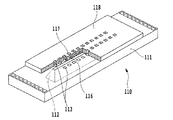
図10は、記録素子基板110の構成を一部分解した状態で説明するための斜視図である。記録素子基板110は、厚さ0.5〜1mmのSi基板111を備え、Si基板111には溝状の貫通口からなるインク供給口112が、Siの結晶方位を利用した異方性エッチングやサンドブラストなどの方法によって形成されている。また、Si基板111上のインク供給口112を挟んだ両側には、電気熱変換素子113が記録解像度に対応したピッチで配列されており、これに電力を供給するためのAl等の電気配線とともに、フォトリソ技術により形成されている。Si基板111上には、供給されたインクを吐出口117まで導くためのインク流路116が形成された流路形成部材118が、吐出口117と電気熱変換素子113が対向するように配置されている。1つの記録素子は、電気熱変換素子113、インク流路116および吐出口117によって構成される。インク供給口112からインク流路116まで導かれたインクは、個々の電気熱変換素子113で発生する気泡の成長エネルギによって、吐出口117より滴となって吐出される。記録動作に伴って消費されたインクは、記録素子基板110と連結された配設部材120のインクタンクから安定して供給される仕組みになっている。
FIG. 10 is a perspective view for explaining the structure of the
配設部材120は、このように記録素子基板110にインクを供給する役割を果たすが、これとともに記録素子基板110を定位置に配設し、支持する役割も果たしている。よって、配設部材120と記録素子基板110は所定の相対位置に、水平垂直方向共に精度よく配置されることが望まれる。具体的には、まず、記録素子基板110のインク供給口112が、配設部材120に形成されたインク供給路の位置に正確に配置されることが望まれる。また、記録素子基板110に配列する複数の記録素子の配列方向が、記録ヘッド1の主走査方向に対し垂直な方向に配列することが望まれる。更に、記録素子基板110の吐出口面が配設部材120の配設面121に対し、平行に配置されることが望まれる。この3番目の条件が満たされないと、吐出口が形成された面が記録媒体面に対し傾きを持つことになるので、吐出されるインクも傾いた状態で記録媒体に着弾し、画像を劣化させる要因となる。
The
但し、一般に配設部材120はコストや加工性等の点からモールド成型品であるため、配設面121には複雑な三次元形状が現れ、理想的な平滑性が得られない場合が多い。そして、平滑性に乏しい配設面121に、そのまま記録素子基板110を接着すると、吐出口が形成された面の傾きは三次元形状の微小な凹凸の影響を直に受け、水平性を確保することが困難になる。
However, since the
例えば、特許文献2では、配設面121に複数個の凸平面部を設け、当該凸平面部について、その平面性を良好な状態に保つことで、吐出口が形成された面の平行性を向上させる技術が開示されている。このような構成であれば、凸平面部以外の配設面121に三次元形状の凹凸が含まれていたとしても、吐出口が形成された面の水平性を確保することが出来る。
For example, in
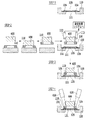
また、近年では、CCDカメラなどを利用して記録素子基板110を配設面121に対して水平垂直方向に正確に位置合わせしておきながら、両者の間に介在する接着剤を紫外線によって硬化させる方法も採用されている。
In recent years, the
図11は、上記方法を採用した記録ヘッドの組み立て工程を説明するための図である。まず、STEP1によって、配設部材120の配設面121に熱硬化接着剤125を塗布する。次に、STEP2において、ギャングボンディング法により電気配線基板と電気接続された記録素子基板110を、供給フィンガー600で吸着し、配設部材120の上方に移動させる。更に、STEP2において、2つのCCDカメラを備えた画像処理システムを用いて記録素子基板110を水平垂直方向に正確に位置合わせする。
FIG. 11 is a view for explaining an assembly process of a recording head employing the above method. First, the
続くSTEP3では、記録素子基板110を下降させ熱硬化接着剤125にこれを当接させる。このとき記録素子基板110は、配設部材120に完全には当接せず、熱硬化接着剤150中に浮いた状態となっている。その後、STEP4において、上記姿勢を保持したまま、光照射機620によって紫外線を照射し、記録素子基板110を昇温させる。これにより、記録素子基板110に接触する熱硬化接着剤125は徐々に硬化し、記録素子基板H1100と配設部材120とを接着固定する。最後に、記録素子基板110周辺と電気接続部を封止剤で封止し、熱キュアを施す事により記録ヘッドが完成する。
In
このような方法によれば、配設面121に微小な凹凸があっても、凹凸の高低差以上の均一な厚みを有する接着剤層によって、記録素子基板110の吐出口が形成された面を配設面121に対し水平に接着することが出来る。なお、以上説明したような、CCDや熱硬化接着剤を用いた記録素子基板の接着方法は、例えば特許文献3に開示されている。
According to such a method, even if the
しかしながら、特許文献2の方法であっても、複数の凸平面部同士の高さには、どうしてもある程度のばらつき含まれる。そして、その程度が近年要求されるような高水準の水平性を実現することを困難にしている。具体的には、凸平面部同士の高さのばらつきは、記録位置精度の観点からは10μm以下に抑えたいが、実際のモールド成型では、どうしても20μm程度のばらつきが発生してしまう。
However, even with the method of
一方、凹凸の高低差以上の接着剤層を形成する構成であれば、複数の凸平面部を設けることなく、記録素子基板110の吐出口面を配設面121に対し平行に接着することが可能である。具体的には、モールド成型品の配設面121には50μm程度の凹凸が存在するが、これよりも大きな70μm程度の厚さを有する接着層を形成すれば、凹凸に左右されることなく記録素子基板110を水平に固定することが出来る。
On the other hand, in the configuration in which an adhesive layer having an uneven height difference or higher is formed, the discharge port surface of the
ただし、接着層の厚みを大きくすると、熱硬化接着剤が充分な強度まで硬化するまでに必要な熱量、すなわち硬化のために要される時間が増大する。その結果、インクジェット記録ヘッドを量産するに当たり、タイムコストの上昇が招致されてしまう。 However, when the thickness of the adhesive layer is increased, the amount of heat required for the thermosetting adhesive to cure to a sufficient strength, that is, the time required for curing increases. As a result, an increase in time cost is incurred when mass-producing inkjet recording heads.
本発明は上記問題点を解決するためになされたものである。よってその目的とするところは、より短い時間で記録素子基板を配設面に対し精度良く接着することが可能なインクジェット記録ヘッドの製造方法を提供することである。 The present invention has been made to solve the above problems. Therefore, an object of the present invention is to provide a method of manufacturing an ink jet recording head that can adhere the recording element substrate to the arrangement surface with a high accuracy in a shorter time.
上記課題を解決するための本発明は、インクを吐出するためのエネルギを発生する記録素子を備えた記録素子基板と、該記録素子基板を配設するための配設面を備えた配設部材と、前記記録素子基板の接着がなされる面と前記配設面との間に介在することにより、前記記録素子基板と前記配設部材とを接着するための接着剤とを備えたインクジェット記録ヘッドであって、前記配設面には少なくとも1つの、先端が前記接着がなされる面と平行な平面である凸部、が設けられ、前記接着剤は前記接着がなされる面と前記平面との間にも介在していることを特徴とする。 In order to solve the above-mentioned problems, the present invention provides a recording element substrate having a recording element that generates energy for discharging ink, and an arrangement member having an arrangement surface for arranging the recording element substrate. And an adhesive for adhering the recording element substrate and the arrangement member by interposing between the surface on which the recording element substrate is adhered and the arrangement surface The arrangement surface is provided with at least one convex portion whose tip is a plane parallel to the surface to be bonded, and the adhesive is formed between the surface to be bonded and the plane. It is also characterized by being interposed between them.
また、インクを吐出するためのエネルギを発生する記録素子を備えた記録素子基板と、該記録素子基板を配設するための配設面と、該配設面に設けられた少なくとも1つの、先端が平面である凸部と、を含む配設部材とを備えたインクジェット記録ヘッドの製造方法であって、前記配設面と前記平面とに接着剤を設ける工程と、前記記録素子基板の接着がなされる面と前記平面とが平行となる様に、前記記録素子基板を前記接着剤に当接させる工程と、前記接着剤を硬化させる硬化工程とを有することを特徴とする。 Further, a recording element substrate including a recording element that generates energy for ejecting ink, an arrangement surface for arranging the recording element substrate, and at least one tip provided on the arrangement surface And a projecting portion including a convex portion, and a method of manufacturing an ink jet recording head comprising: a step of providing an adhesive on the placement surface and the plane; and bonding of the recording element substrate. The method includes a step of bringing the recording element substrate into contact with the adhesive and a curing step of curing the adhesive so that the surface to be formed and the plane are parallel to each other.
本発明によれば、記録素子基板と配設部材の接着面の中に熱硬化接着剤層の薄い箇所を部分的に設けることにより、比較的短時間で記録素子基板を配設部材に接着することが可能となる。よって、配設面に凹凸が存在する場合であっても、精度の高い状態で記録素子基板と配設部材を短時間で接着固定し、記録ヘッドの量産性を向上させることが可能となる。 According to the present invention, the recording element substrate is bonded to the arrangement member in a relatively short time by partially providing a thin portion of the thermosetting adhesive layer in the bonding surface between the recording element substrate and the arrangement member. It becomes possible. Therefore, even if there is unevenness on the arrangement surface, the recording element substrate and the arrangement member can be bonded and fixed in a short time with high accuracy, and the mass productivity of the recording head can be improved.
(実施例1)
以下に、本実施形態の記録ヘッドおよびその製造方法を詳しく説明する。
Example 1
Hereinafter, the recording head of this embodiment and the manufacturing method thereof will be described in detail.
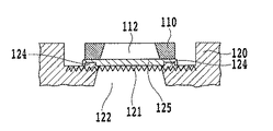
図1は、本実施例のインクジェット記録ヘッドにおける配設部材120と、吐出口や吐出のためのエネルギを発生する電気熱変換素子を配した記録素子基板110の接着状態を説明するための断面図である。また、図2は接着前の配設部材120の配設面121近傍の概略を説明するための上面図である。
FIG. 1 is a cross-sectional view for explaining an adhesion state of a
記録素子基板110を配設するための配設面121はモールド成型品であり、その中央には、インク供給路122が備えられている。記録素子基板110を破線で示した接続位置123に精度よく設置することにより、インク供給路122と記録素子基板110のインク供給口112が連結し、記録素子基板110にインクを安定して供給することが出来るようになる。
An
本実施例において、接続位置123の長手方向の両端には、先端が平面である凸平面部124が2箇所形成されている。このような凸平面部124を設けることにより、凸平面部における記録素子基板110と配設面121の間に介在する熱硬化接着剤125の厚さを凸平面部以外の領域に比べて薄くすることが出来る。このように凸平面部を部分的に形成することで、後述するようにその部位の平面度ばらつきを抑えることが可能となる。平面度のばらつきを抑えるためには、その先端が接着される凸平面部の面積は小さいほうが好ましく、凸平面部同士のばらつきの影響を考慮すると、凸平面部の数は複数であっても少ないほうが好ましい。本実施例のように凸平面部を2個所とすることで凸平面部の平面度を高く保ちつつ、接続位置123の長手方向の両端に1つずつ形成することで、記録素子基板の平面の維持が可能となり好ましい。
In the present embodiment, two convex
図3は配設部材H1200を形成するのに用いる型500の構成を説明するための概略断面図である。図に示すように、型500は、外側駒510、内側駒530および凸平面部駒520の3つの部分から構成され、精度を必要とする凸平面部駒は入れ子構造となっている。
FIG. 3 is a schematic cross-sectional view for explaining the configuration of a
図4(a)〜(c)は、凸平面部駒520において、凸平面部124を形成する工程を説明するための概略図である。図4(a)は、切削形成することによって凸平面部124以外の形状が形成された平面部駒520の側面と上面を示している。
4A to 4C are schematic views for explaining a process of forming the convex
このような状態の平面部駒520の凸部予定箇所521に対し、放電加工を行うことにより、図4(b)に示すような凸平面部の形状が形成される。更に、形成された型を用いて成形された配設部材の凸平面部の精度を測定し、ずれた分だけ再び放電加工によって凸部の高さ補正を行う。これにより、凸平面部のための型が完成する(図4(c))。
By performing electric discharge machining on the projected projected
本実施例において、型の成形材料としては、例えば変性ポリフェニレンエーテルを用いることが出来る。この場合、配設面121から凸平面部124の上面までの高さを0.05mmとし、凸平面部124の平面度のばらつきは0.015mm程度に抑えることが出来る。
In the present embodiment, for example, modified polyphenylene ether can be used as a molding material for the mold. In this case, the height from the
図5は、記録ヘッドの一連の組み立て工程のうち、凸平面部124を持つ配設面121に、記録素子基板110を、熱硬化接着剤を介して接着固定する工程を説明するための図である。
FIG. 5 is a diagram for explaining a process of bonding and fixing the
まず、STEP1において、配設部材120の配設面121に熱硬化接着剤125を塗布する。このとき使用される熱硬化接着剤としては、粘度が高く、インク供給口等に流れ込まない性質を持つものが望ましい。
First, in
続くSTEP2において、記録素子基板110を治具(供給フィンガー600)で吸着し、配設面121の上方にこれを移動する。そして、CCDカメラなどを備えた画像処理システムを利用して、記録素子基板110の位置調整を行う。ここで行う位置調整によって、記録素子基板110のインク供給口112は、配設部材120に形成されたインク供給路122と連通可能となる。また、記録素子基板110は配設面121に対して平行に配置される。
In
STEP3では、供給フィンガー600を下降させて、記録素子基板110を凸平面部124の上面から20μm程度離れた位置に配置し、熱硬化接着剤125と当接させる。この状態において熱硬化接着剤125は未だ硬化していないので、調整した位置から記録素子基板110がずれないように、供給フィンガー600によって記録素子基板110を吸着したまま、その姿勢を保持する。
In
その後、STEP4において、記録素子基板表面121の供給フィンガーに覆われていない部分に、光照射機620によって光を照射する。本実施例では、光源にUV光を使用し、記録素子基板110の短手側面端近傍の2箇所に8000mW/cm2(365nm波長)の光を照射する。この照射により、記録素子基板110は昇温し、記録素子基板110の裏面に存在する熱硬化接着剤125は硬化して、記録素子基板110と配設部材120は上記調整された位置で接着固定される。すなわち、凸平面部124の平面度のばらつきは0.015mm程度存在するが、記録素子基板110はこの凹凸に影響されること無く、配設部材120の凸平面部124の上面から約0.020mm(20μm)離れた位置にて、水平に固定される。また、2箇所の凸平面部124上に存在する熱硬化接着剤は、STEP4の硬化工程において厚みが少ない分、平面以外の他の部分よりも早期に硬化する。よって、結果的に、記録素子基板110が配設部材120に必要な強度で接着固定されるまでの光照射時間を、凸平面部を設けない場合に比べて短縮することが出来る。
Thereafter, in
本実施例の場合は、凸平面部を設けない場合に比べて光照射時間を約20%短縮することが出来、記録ヘッド自体の量産性を従来よりも向上させることが可能となった。また本実施例においては、凸平面部を配設部材120における接続位置123(図2参照)の長手方向の両端に形成したので、記録素子基板110の両端部から接着剤が硬化する。よって、短時間(約2秒)でその部位の接着剤が硬化するとともに、配設部材120と記録素子基板110との水平性を精度良く保つことが可能となる。このような構成は記録素子基板110が長くなるほど有効となる。特に記録素子基板の長手方向の長さが0.85インチ以上になると記録素子基板の平面性を維持することが難しくなるので本実施例の構成は好ましい。
In the case of this embodiment, the light irradiation time can be shortened by about 20% compared to the case where the convex flat portion is not provided, and the mass productivity of the recording head itself can be improved as compared with the conventional case. In this embodiment, since the convex flat portions are formed at both ends in the longitudinal direction of the connection position 123 (see FIG. 2) in the
また凸平面部以外の部位に配されている熱硬化接着剤は、この時点ではすべて硬化していなくてもよい。つまり凸平面部にある相対的に薄い熱硬化接着剤のみが硬化していれば良いものである。その他の部位の接着剤については、例えば、記録素子基板110と電気配線基板130との電気接続部を封止した後に100℃で1時間程度の加熱を行い、熱硬化接着剤を完全に硬化させればよい。
Further, all of the thermosetting adhesive disposed in the portion other than the convex flat portion may not be cured at this point. That is, it is only necessary that only a relatively thin thermosetting adhesive on the convex flat portion is cured. For the adhesive in other parts, for example, after sealing the electrical connection portion of the
(実施例2)
図6は、本実施例のインクジェット記録ヘッドにおける配設部材120と記録素子基板110の接着状態を説明するための断面図である。また、Fig.7は接着前の配設部材120の配設面121近傍の概略を説明するための上面図である。本実施例では、接続位置123の略中央に2つの凸平面部126が形成されている。このような位置に凸平面部を設けることにより、記録素子基板110と配設面121の間の熱硬化接着剤125の厚みを部分的に薄くした接着部分を設けることが出来る。
(Example 2)
FIG. 6 is a cross-sectional view for explaining the bonding state between the disposing
図8は、本実施例の記録ヘッドの一連の組み立て工程のうち、凸平面部126を持つ配設面121に記録素子基板110を接着固定する工程を説明するための図である。
FIG. 8 is a diagram for explaining a step of bonding and fixing the
まず、STEP1において、配設部材120の配設面121に熱硬化接着剤125を塗布する。このとき使用される熱硬化接着剤としては、実施例1と同様、粘度が高く、インク供給口等に流れ込まない性質を持つものが望ましい。
First, in
続くSTEP2において、内蔵されたヒータ601によって既に一定温度(本実施例では150℃)に加熱された供給フィンガー600を用い、記録素子基板110を吸着し、配設面121の上方にこれを移動する。そして、CCDカメラなどを備えた画像処理システムを利用して、記録素子基板110の位置調整を行う。ここで行う位置調整によって、記録素子基板110のインク流路は、配設部材120に形成されたインク供給路122と連通可能となる。また、記録素子基板110は配設面121に対して平行に配置される。
In
STEP3では、供給フィンガー600を下降させて、記録素子基板110を凸平面部126の上面から20μm程度離れた位置に配置し、熱硬化接着剤125と当接させる。本実施例では、記録素子基板110が既に加熱されているので、これが熱効果接着剤125に当接した瞬間から、熱硬化接着剤125の硬化は開始する。充分に熱硬化接着剤が硬化するまでの間、記録素子基板110が調整した位置からずれないように、供給フィンガー600は記録素子基板110を吸着した状態でその姿勢を維持する。少なくとも記録素子基板110と凸平面部126の間の熱硬化接着剤125が充分に硬化したら、供給フィンガー600による記録素子基板110の吸着を解除する。
In
以上説明した工程により、記録素子基板110と配設部材120は上記調整された位置で接着固定される。凸平面部126の平面度のばらつきは0.015mm程度存在するが、記録素子基板110はこの凹凸に影響されること無く、配設部材120の凸平面部126の上面から約20μm離れた位置にて、ほぼ水平に固定される。また、凸平面部126上に存在する熱硬化接着剤は、STEP3の硬化工程において、厚みが少ない分他の部分よりも早期に硬化する。
Through the steps described above, the
更に本実施例では、熱硬化接着剤125と当接する以前から記録素子基板110が加熱されているので、上述した実施例1よりも、記録素子基板110が配設部材120に必要な強度で接着固定されるまでの時間を更に短縮することが期待出来る。また本実施例のように過熱された供給フィンガーを使用する際には、凸平面部を供給フィンガーと記録素子基板との吸着領域に対応する部位に設けることが伝熱を考慮すると好ましい。特に供給フィンガーからの熱をすみやかに記録素子基板に伝熱する点を考慮すると、凸平面部を配設部材120における記録素子基板110の中央部に対応する位置に2箇所形成することが好ましい。
Furthermore, in this embodiment, since the
なお、以上の実施例では、光源にUV光を使用したり、直接記録素子基板を加熱したりしたが、使用する熱硬化接着剤が硬化するに充分な熱量が得られさえすれば、どのような手段で、熱硬化接着剤を過熱しても構わない。例えば、赤外線等の他の光源を使用することも可能である。 In the above embodiment, UV light is used as the light source or the recording element substrate is directly heated. However, as long as a sufficient amount of heat can be obtained for the thermosetting adhesive to be used, what is necessary? The thermosetting adhesive may be overheated by any means. For example, other light sources such as infrared light can be used.
また、上記実施例では、成形材料として変性ポリフェニレンエーテルを用い、配設面121から凸平面部126の上面までの高さを0.05mmとしたが、本発明はこれに限定されるものではない。配設面121から凸平面部126の上面までの高さは、数値的には0.01〜0.20mm位が望ましいが、成形材料特性、金型精度、熱硬化接着剤の物性値等を考慮して適切な値に調整されれば本発明は有効に機能する。
Moreover, in the said Example, although modified polyphenylene ether was used as a molding material and the height from the arrangement | positioning
更に、凸平面部を形成する位置も上記2つの実施例に限定されるものではない。凸平面部を設けた箇所の熱硬化接着剤をなるべく早い時期に硬化させるように、記録素子基板の凸平面部に対応する部分が効果的に加熱されれば、本発明の効果は充分得ることが出来る。 Furthermore, the position where the convex flat portion is formed is not limited to the above two embodiments. If the portion corresponding to the convex flat portion of the recording element substrate is effectively heated so that the thermosetting adhesive at the location where the convex flat portion is provided is cured as early as possible, the effect of the present invention can be sufficiently obtained. I can do it.
また、記録素子基板を精度良く接着するためには、凸平面部を3箇所設けることも好ましい。この場合、凸平面部を、インク供給路122の一方の側の領域の接続位置123の長手方向の両端部に2つ、インク供給路の他方の側の領域の、接続位置123の長手方向の中央部に1つ、凸平面部を設けることが好ましい。
In order to bond the recording element substrate with high accuracy, it is also preferable to provide three convex flat portions. In this case, two convex flat portions are provided at both ends in the longitudinal direction of the
以上説明したように本発明によれば、記録素子基板と配設部材の接着面の中に接着剤層の薄い箇所を部分的に設け、記録素子基板と配設部材の相対的な位置を調整した後に、上記薄い箇所の接着剤層を硬化させる。これにより、比較的短時間で記録素子基板を配設部材に精度よく接着することが可能となる。結果、配設面に凹凸が存在する場合であっても、精度の高い状態で記録ヘッドの量産性を向上させることが可能となる。 As described above, according to the present invention, a thin portion of the adhesive layer is partially provided in the bonding surface between the recording element substrate and the arrangement member, and the relative position between the recording element substrate and the arrangement member is adjusted. Then, the thin adhesive layer is cured. As a result, the recording element substrate can be accurately bonded to the arrangement member in a relatively short time. As a result, it is possible to improve the mass productivity of the recording head with high accuracy even when there are irregularities on the arrangement surface.
1 インクジェット記録ヘッド
110 記録素子基板
112 インク供給口
113 電気熱変換素子
116 インク流路
117 吐出口
111 Siウェハー
120 配設部材
121 配設面
122 インク供給路
123 接着位置
124 凸平面部
125 熱硬化接着剤
126 凸平面部
130 電気配線基板
500 型
510 外側駒
520 平面部駒
521 凸部予定箇所
530 内側駒
600 供給フィンガー
601 ヒータ
620 光照射機
DESCRIPTION OF
Claims (11)
該記録素子基板を配設するための配設面を備えた配設部材と、
前記記録素子基板の接着がなされる面と前記配設面との間に介在することにより、前記記録素子基板と前記配設部材とを接着するための接着剤と
を備えたインクジェット記録ヘッドであって、
前記配設面には少なくとも1つの、先端が前記接着がなされる面と平行な平面である凸部、が設けられ、前記接着剤は前記接着がなされる面と前記平面との間にも介在していることを特徴とするインクジェット記録ヘッド。 A recording element substrate including a recording element that generates energy for discharging ink;
An arrangement member having an arrangement surface for arranging the recording element substrate;
An ink jet recording head comprising an adhesive for adhering the recording element substrate and the arrangement member by interposing between the surface on which the recording element substrate is adhered and the arrangement surface. And
The arrangement surface is provided with at least one convex portion whose tip is a plane parallel to the surface to be bonded, and the adhesive is interposed between the surface to be bonded and the plane. An ink jet recording head.
該記録素子基板を配設するための配設面と、該配設面に設けられた少なくとも1つの、先端が平面である凸部と、を含む配設部材と
を備えたインクジェット記録ヘッドの製造方法であって、
前記配設面と前記平面とに接着剤を設ける工程と、
前記記録素子基板の接着がなされる面と前記平面とが平行となる様に、前記記録素子基板を前記接着剤に当接させる工程と、
前記接着剤を硬化させる硬化工程と
を有することを特徴とするインクジェット記録ヘッドの製造方法。 A recording element substrate including a recording element that generates energy for discharging ink;
Manufacture of an inkjet recording head comprising an arrangement surface for arranging the recording element substrate and an arrangement member including at least one convex portion provided on the arrangement surface and having a flat tip. A method,
Providing an adhesive on the arrangement surface and the plane;
Contacting the recording element substrate with the adhesive so that the plane on which the recording element substrate is bonded is parallel to the plane;
A method for manufacturing an ink jet recording head, comprising: a curing step for curing the adhesive.
Priority Applications (4)
| Application Number | Priority Date | Filing Date | Title |
|---|---|---|---|
| JP2009113565A JP5464901B2 (en) | 2008-06-06 | 2009-05-08 | Ink jet recording head and manufacturing method thereof |
| US12/472,889 US8272130B2 (en) | 2008-06-06 | 2009-05-27 | Method of manufacturing an ink jet print head |
| CN2009101473035A CN101607477B (en) | 2008-06-06 | 2009-06-05 | Ink jet print head and method of manufacturing the same |
| US13/556,389 US9802410B2 (en) | 2008-06-06 | 2012-07-24 | Ink jet print head |
Applications Claiming Priority (3)
| Application Number | Priority Date | Filing Date | Title |
|---|---|---|---|
| JP2008149376 | 2008-06-06 | ||
| JP2008149376 | 2008-06-06 | ||
| JP2009113565A JP5464901B2 (en) | 2008-06-06 | 2009-05-08 | Ink jet recording head and manufacturing method thereof |
Publications (2)
| Publication Number | Publication Date |
|---|---|
| JP2010012774A true JP2010012774A (en) | 2010-01-21 |
| JP5464901B2 JP5464901B2 (en) | 2014-04-09 |
Family
ID=41399919
Family Applications (1)
| Application Number | Title | Priority Date | Filing Date |
|---|---|---|---|
| JP2009113565A Active JP5464901B2 (en) | 2008-06-06 | 2009-05-08 | Ink jet recording head and manufacturing method thereof |
Country Status (3)
| Country | Link |
|---|---|
| US (2) | US8272130B2 (en) |
| JP (1) | JP5464901B2 (en) |
| CN (1) | CN101607477B (en) |
Families Citing this family (15)
| Publication number | Priority date | Publication date | Assignee | Title |
|---|---|---|---|---|
| JP5738018B2 (en) * | 2011-03-10 | 2015-06-17 | キヤノン株式会社 | Ink jet recording head and manufacturing method thereof |
| JP5828682B2 (en) * | 2011-06-06 | 2015-12-09 | キヤノン株式会社 | Method for manufacturing liquid discharge head |
| KR101827070B1 (en) | 2013-02-28 | 2018-02-07 | 휴렛-팩커드 디벨롭먼트 컴퍼니, 엘.피. | Molding a fluid flow structure |
| KR20150112029A (en) | 2013-02-28 | 2015-10-06 | 휴렛-팩커드 디벨롭먼트 컴퍼니, 엘.피. | Molded print bar |
| KR20180086281A (en) | 2013-02-28 | 2018-07-30 | 휴렛-팩커드 디벨롭먼트 컴퍼니, 엘.피. | Molded fluid flow structure |
| US10632752B2 (en) | 2013-02-28 | 2020-04-28 | Hewlett-Packard Development Company, L.P. | Printed circuit board fluid flow structure and method for making a printed circuit board fluid flow structure |
| US10821729B2 (en) | 2013-02-28 | 2020-11-03 | Hewlett-Packard Development Company, L.P. | Transfer molded fluid flow structure |
| US10029467B2 (en) | 2013-02-28 | 2018-07-24 | Hewlett-Packard Development Company, L.P. | Molded printhead |
| US9539814B2 (en) | 2013-02-28 | 2017-01-10 | Hewlett-Packard Development Company, L.P. | Molded printhead |
| US9724920B2 (en) | 2013-03-20 | 2017-08-08 | Hewlett-Packard Development Company, L.P. | Molded die slivers with exposed front and back surfaces |
| JP6137918B2 (en) | 2013-04-12 | 2017-05-31 | キヤノン株式会社 | Inkjet recording head and inkjet recording apparatus |
| JP2014240136A (en) * | 2013-06-11 | 2014-12-25 | キヤノン株式会社 | Method of manufacturing liquid discharge head, and liquid discharge head |
| JP6433263B2 (en) * | 2014-01-14 | 2018-12-05 | キヤノン株式会社 | Method for manufacturing liquid discharge head |
| JP6719911B2 (en) * | 2016-01-19 | 2020-07-08 | キヤノン株式会社 | Liquid ejection head manufacturing method |
| US20210316553A1 (en) * | 2018-11-21 | 2021-10-14 | Hewlett-Packard Development Company, L.P. | Curved fluid ejection modules |
Citations (4)
| Publication number | Priority date | Publication date | Assignee | Title |
|---|---|---|---|---|
| JP2004047573A (en) * | 2002-07-09 | 2004-02-12 | Canon Inc | Laser light source equipment |
| JP2005138306A (en) * | 2003-11-04 | 2005-06-02 | Canon Inc | Inkjet head |
| JP2006003563A (en) * | 2004-06-16 | 2006-01-05 | Ricoh Co Ltd | Alignment bonding method and alignment bonding apparatus |
| JP2007290243A (en) * | 2006-04-25 | 2007-11-08 | Canon Inc | Inkjet recording head, and manufacturing method for inkjet recording head |
Family Cites Families (12)
| Publication number | Priority date | Publication date | Assignee | Title |
|---|---|---|---|---|
| JPH04345858A (en) * | 1991-05-23 | 1992-12-01 | Seiko Epson Corp | Fabrication of ink jet head |
| US5852460A (en) * | 1995-03-06 | 1998-12-22 | Hewlett-Packard Company | Inkjet print cartridge design to decrease deformation of the printhead when adhesively sealing the printhead to the print cartridge |
| JP3437425B2 (en) | 1997-11-17 | 2003-08-18 | キヤノン株式会社 | Ink jet recording head and ink jet recording apparatus |
| US6241335B1 (en) * | 1997-12-24 | 2001-06-05 | Canon Kabushiki Kaisha | Method of producing ink jet recording head and ink jet recording head produced by the method |
| DE19856333A1 (en) * | 1998-12-07 | 2000-06-08 | Bosch Gmbh Robert | Gluing process |
| US6652702B2 (en) | 2000-09-06 | 2003-11-25 | Canon Kabushiki Kaisha | Ink jet recording head and method for manufacturing ink jet recording head |
| JP4780875B2 (en) | 2000-09-06 | 2011-09-28 | キヤノン株式会社 | Method for manufacturing ink jet recording head |
| JP4338202B2 (en) | 2004-06-02 | 2009-10-07 | キヤノン株式会社 | Liquid discharge head and liquid discharge apparatus including the same |
| JP4137088B2 (en) | 2004-06-02 | 2008-08-20 | キヤノン株式会社 | Head substrate, recording head, head cartridge, recording apparatus, and information input / output method |
| CN100503248C (en) | 2004-06-02 | 2009-06-24 | 佳能株式会社 | Head substrate, recording head, head cartridge, recorder, and method for inputting/outputting information |
| JP4194580B2 (en) | 2004-06-02 | 2008-12-10 | キヤノン株式会社 | Head substrate, recording head, head cartridge, and recording apparatus |
| JP5322719B2 (en) | 2008-03-24 | 2013-10-23 | キヤノン株式会社 | Inkjet recording head |
-
2009
- 2009-05-08 JP JP2009113565A patent/JP5464901B2/en active Active
- 2009-05-27 US US12/472,889 patent/US8272130B2/en not_active Expired - Fee Related
- 2009-06-05 CN CN2009101473035A patent/CN101607477B/en active Active
-
2012
- 2012-07-24 US US13/556,389 patent/US9802410B2/en active Active
Patent Citations (4)
| Publication number | Priority date | Publication date | Assignee | Title |
|---|---|---|---|---|
| JP2004047573A (en) * | 2002-07-09 | 2004-02-12 | Canon Inc | Laser light source equipment |
| JP2005138306A (en) * | 2003-11-04 | 2005-06-02 | Canon Inc | Inkjet head |
| JP2006003563A (en) * | 2004-06-16 | 2006-01-05 | Ricoh Co Ltd | Alignment bonding method and alignment bonding apparatus |
| JP2007290243A (en) * | 2006-04-25 | 2007-11-08 | Canon Inc | Inkjet recording head, and manufacturing method for inkjet recording head |
Also Published As
| Publication number | Publication date |
|---|---|
| US8272130B2 (en) | 2012-09-25 |
| CN101607477A (en) | 2009-12-23 |
| CN101607477B (en) | 2011-10-05 |
| US20120287205A1 (en) | 2012-11-15 |
| US9802410B2 (en) | 2017-10-31 |
| JP5464901B2 (en) | 2014-04-09 |
| US20090303278A1 (en) | 2009-12-10 |
Similar Documents
| Publication | Publication Date | Title |
|---|---|---|
| JP5464901B2 (en) | Ink jet recording head and manufacturing method thereof | |
| TW201836050A (en) | Component mounting system, resin shaping device, resin placing device, component mounting method, and resin shaping method | |
| US20090009559A1 (en) | Liquid ejection head and method for manufacturing liquid ejection head | |
| JP3850370B2 (en) | Inkjet head unit and manufacturing method thereof | |
| KR20110113739A (en) | Illumination system for use in a stereolithography apparatus | |
| TW200426037A (en) | Liquid drop emission device, and liquid drop emission method | |
| JP2009298108A (en) | Method for manufacturing inkjet recording head, and inkjet recording head | |
| JP2010089498A (en) | Method for manufacturing inkjet recording head | |
| JP4205140B2 (en) | Ink jet head and method of manufacturing ink jet head | |
| US7527347B2 (en) | Ink jet print head and ink jet printing apparatus having a plurality of slits formed in a heater substrate mounting surface | |
| JP2010284908A (en) | Inkjet head and method for manufacturing the same | |
| JP2018176580A (en) | Liquid ejection head and its manufacturing method | |
| JP2007076226A (en) | Liquid droplet discharging head, and its manufacturing method | |
| JP7195829B2 (en) | Manufacturing method of liquid ejection head and liquid ejection device | |
| WO2018138755A1 (en) | Circuit forming method and circuit forming device | |
| JP2008093902A (en) | Transfer method of thin film diaphragm and inkjet recorder using it | |
| JP2018083365A (en) | Liquid discharge head and manufacturing method of liquid discharge head | |
| WO2013088505A1 (en) | Liquid discharge head and method for producing same | |
| JP2014188985A (en) | Method for manufacturing module bracket combined body | |
| JP2011110792A (en) | Method for manufacturing liquid ejection head | |
| JP2007250761A (en) | Manufacturing method of semiconductor device | |
| JP6728439B1 (en) | Liquid ejection head and manufacturing method thereof | |
| JP2019202470A (en) | Manufacturing method of liquid discharge head | |
| JPH09183229A (en) | Manufacture of ink-jet head, ink-jet head manufactured by same method, and ink-jet apparatus equipped with same ink-jet head | |
| JP5279355B2 (en) | Method for manufacturing liquid ejection device |
Legal Events
| Date | Code | Title | Description |
|---|---|---|---|
| RD02 | Notification of acceptance of power of attorney |
Free format text: JAPANESE INTERMEDIATE CODE: A7422 Effective date: 20101106 |
|
| A621 | Written request for application examination |
Free format text: JAPANESE INTERMEDIATE CODE: A621 Effective date: 20120423 |
|
| A131 | Notification of reasons for refusal |
Free format text: JAPANESE INTERMEDIATE CODE: A131 Effective date: 20130416 |
|
| A977 | Report on retrieval |
Free format text: JAPANESE INTERMEDIATE CODE: A971007 Effective date: 20130417 |
|
| A521 | Written amendment |
Free format text: JAPANESE INTERMEDIATE CODE: A523 Effective date: 20130617 |
|
| A131 | Notification of reasons for refusal |
Free format text: JAPANESE INTERMEDIATE CODE: A131 Effective date: 20130723 |
|
| A521 | Written amendment |
Free format text: JAPANESE INTERMEDIATE CODE: A523 Effective date: 20130924 |
|
| TRDD | Decision of grant or rejection written | ||
| A01 | Written decision to grant a patent or to grant a registration (utility model) |
Free format text: JAPANESE INTERMEDIATE CODE: A01 Effective date: 20131224 |
|
| A61 | First payment of annual fees (during grant procedure) |
Free format text: JAPANESE INTERMEDIATE CODE: A61 Effective date: 20140121 |
|
| R151 | Written notification of patent or utility model registration |
Ref document number: 5464901 Country of ref document: JP Free format text: JAPANESE INTERMEDIATE CODE: R151 |