JP2010009353A - Semiconductor integrated circuit, ic card mounted with the semiconductor integrated circuit, and operation method for the same - Google Patents
Semiconductor integrated circuit, ic card mounted with the semiconductor integrated circuit, and operation method for the same Download PDFInfo
- Publication number
- JP2010009353A JP2010009353A JP2008168471A JP2008168471A JP2010009353A JP 2010009353 A JP2010009353 A JP 2010009353A JP 2008168471 A JP2008168471 A JP 2008168471A JP 2008168471 A JP2008168471 A JP 2008168471A JP 2010009353 A JP2010009353 A JP 2010009353A
- Authority
- JP
- Japan
- Prior art keywords
- circuit
- signal
- demodulation
- reception
- received
- Prior art date
- Legal status (The legal status is an assumption and is not a legal conclusion. Google has not performed a legal analysis and makes no representation as to the accuracy of the status listed.)
- Granted
Links
- 238000000034 method Methods 0.000 title claims description 97
- 239000004065 semiconductor Substances 0.000 title claims description 41
- 238000004891 communication Methods 0.000 claims abstract description 146
- 230000005540 biological transmission Effects 0.000 claims description 123
- 238000012545 processing Methods 0.000 claims description 69
- 230000015654 memory Effects 0.000 claims description 21
- 230000004044 response Effects 0.000 claims description 21
- 238000012546 transfer Methods 0.000 claims description 20
- 230000007704 transition Effects 0.000 claims description 12
- 238000009499 grossing Methods 0.000 claims description 11
- 239000000758 substrate Substances 0.000 claims description 6
- 238000004148 unit process Methods 0.000 claims description 4
- 238000011017 operating method Methods 0.000 claims 1
- 230000035945 sensitivity Effects 0.000 description 44
- 238000001514 detection method Methods 0.000 description 30
- 238000010586 diagram Methods 0.000 description 29
- 230000008569 process Effects 0.000 description 22
- 238000006243 chemical reaction Methods 0.000 description 18
- 238000013075 data extraction Methods 0.000 description 14
- 230000006870 function Effects 0.000 description 9
- 230000008859 change Effects 0.000 description 7
- 238000005516 engineering process Methods 0.000 description 5
- 239000003990 capacitor Substances 0.000 description 4
- 125000004122 cyclic group Chemical group 0.000 description 4
- 238000003708 edge detection Methods 0.000 description 3
- XUIMIQQOPSSXEZ-UHFFFAOYSA-N Silicon Chemical compound [Si] XUIMIQQOPSSXEZ-UHFFFAOYSA-N 0.000 description 2
- 230000005684 electric field Effects 0.000 description 2
- 239000003999 initiator Substances 0.000 description 2
- 229910052710 silicon Inorganic materials 0.000 description 2
- 239000010703 silicon Substances 0.000 description 2
- 238000005260 corrosion Methods 0.000 description 1
- 230000008878 coupling Effects 0.000 description 1
- 238000010168 coupling process Methods 0.000 description 1
- 238000005859 coupling reaction Methods 0.000 description 1
- 238000011161 development Methods 0.000 description 1
- 230000009977 dual effect Effects 0.000 description 1
- 230000000694 effects Effects 0.000 description 1
- 238000000605 extraction Methods 0.000 description 1
- 239000004973 liquid crystal related substance Substances 0.000 description 1
- 238000010295 mobile communication Methods 0.000 description 1
- 230000008520 organization Effects 0.000 description 1
- 230000002093 peripheral effect Effects 0.000 description 1
- 230000010363 phase shift Effects 0.000 description 1
Images


Classifications
-
- G—PHYSICS
- G06—COMPUTING; CALCULATING OR COUNTING
- G06K—GRAPHICAL DATA READING; PRESENTATION OF DATA; RECORD CARRIERS; HANDLING RECORD CARRIERS
- G06K19/00—Record carriers for use with machines and with at least a part designed to carry digital markings
- G06K19/06—Record carriers for use with machines and with at least a part designed to carry digital markings characterised by the kind of the digital marking, e.g. shape, nature, code
- G06K19/067—Record carriers with conductive marks, printed circuits or semiconductor circuit elements, e.g. credit or identity cards also with resonating or responding marks without active components
- G06K19/07—Record carriers with conductive marks, printed circuits or semiconductor circuit elements, e.g. credit or identity cards also with resonating or responding marks without active components with integrated circuit chips
- G06K19/0723—Record carriers with conductive marks, printed circuits or semiconductor circuit elements, e.g. credit or identity cards also with resonating or responding marks without active components with integrated circuit chips the record carrier comprising an arrangement for non-contact communication, e.g. wireless communication circuits on transponder cards, non-contact smart cards or RFIDs
- G06K19/0724—Record carriers with conductive marks, printed circuits or semiconductor circuit elements, e.g. credit or identity cards also with resonating or responding marks without active components with integrated circuit chips the record carrier comprising an arrangement for non-contact communication, e.g. wireless communication circuits on transponder cards, non-contact smart cards or RFIDs the arrangement being a circuit for communicating at a plurality of frequencies, e.g. for managing time multiplexed communication over at least two antennas of different types
Abstract
Description
本発明は、半導体集積回路、半導体集積回路を実装したICカードおよびその動作方法に関するもので、特に、少なくとも3種類の受信信号のいずれのタイプの受信信号を短時間で受け付けるのに有益な技術に関する。 The present invention relates to a semiconductor integrated circuit, an IC card on which the semiconductor integrated circuit is mounted, and an operation method thereof, and more particularly to a technique useful for receiving any type of received signal of at least three types of received signals in a short time. .
国際規格ISO/IEC14443によれば、非接触インターフェースを有するICカードはPICCと呼ばれ、PCDと呼ばれるリーダー/ライター装置とRF通信を行うものである。尚、ISOはInternational Organization for Standardizationの略であり、IECはInternational Electrical Commissionの略である。また、PICCはProximity Cardの略であり、PCDはProximity Coupling Deviceの略である。 According to the international standard ISO / IEC14443, an IC card having a non-contact interface is called a PICC and performs RF communication with a reader / writer device called a PCD. ISO is an abbreviation for International Organization for Standardization, and IEC is an abbreviation for International Electrical Commission. PICC is an abbreviation for Proximity Card, and PCD is an abbreviation for Proximity Coupling Device.
例えば、下記非特許文献1に記載されているように、国際規格ISO/IEC14443のタイプAでは、PCDからPICCへの通信は、ASK100%の変調度の変調方式で変形ミラー方式による符号化方式とされている。しかし、国際規格ISO/IEC14443のタイプBではPCDからPICCへの通信はASK10%の変調率の変調方式でNRZ−L方式による符号化方式とされている。尚、NRZ−Lは、Non Return to Zero-Levelの略である。尚、ASKは、ディジタル変調方式の1つである振幅偏移変調(Amplitude Shift Keying)である。
For example, as described in Non-Patent
例えば、下記非特許文献2に記載されているように、国際規格ISO/IEC14443では、PICCが動作フィールドに入ってから5m秒以内にリクエストを受け付けることが規定されている。また、タイプAのPICCはタイプBのいかなるコマンドを受信しても、5m秒以内にタイプAのリクエストコマンドを受け付けることが規定されている。同様に、タイプBのPICCはタイプAのいかなるコマンドを受信しても、5m秒以内にタイプBのリクエストコマンドを受け付けることが規定されている。
For example, as described in Non-Patent
更に、下記非特許文献2に記載のように、タイプAの初期化では、タイプAのPICCは、アイドル状態からタイプAのリクエストコマンドによってレディー状態に遷移して、更にレディー状態から選択コマンドによってアクテイブ状態に遷移して、アクテイブ状態からホールトコマンドによって停止状態に遷移する。尚、レディー状態は、アンチコロージョンループを有している。
Further, as described in
また、下記非特許文献2と下記特許文献5とに記載のように、タイプBの初期化ではタイプBのPICCは、アイドル状態でタイプBのリクエストコマンドを待っている。このリクエストコマンドは、タイプBのPICCにアプリケーション・ファミリー・アイデンティファイヤー(AFI)、属性情報パラメータ(PARAM)、巡回冗長チェックコード(CRC)を生成する準備のためのものである。タイプBのPICCがAFIの一致を検出するとタイプBのリクエストに対するレスポンスをPCDに送信する。このレスポンスは、擬似ユニーク・アイデンティファイヤー(PUPI)、アプリケーション情報(アプリケーションデータ)、プロトコール情報、巡回冗長チェックコード(CRC)を含んでいる。その後、タイプBのPICCがPICC選択コマンドを受け付けると、それに対するレスポンスをPCDに送信して、アクテイブ状態に遷移する。更にタイプBの送信データはフレームとしてのキャラクタと呼ばれており、このフレームはSOF(Start Of Frame)とEOF(End Of Frame)とによって境界が定められている。SOFとEOFのそれぞれは、1個の立ち下がりエッジと所定の長さの論理“0”を含んでいる。
Further, as described in
近年、短距離無線通信技術(NFC)と呼ばれ、家電製品、デジタルメディア、消費者向けの無線通信接続、コンテンツ、ビジネス上の取引を簡略化して、かつ拡大させる通信技術が普及している。このNFC技術は既存の種々の通信方式と互換性を持ち、13.56MHzのRF周波数を使用して、10cm程度で最大通信レート847Kbpsの短距離通信を可能とする。特に、電子決済機能を有するICカードマイコン(セキュアチップ)を内蔵する携帯電話端末にNFC技術が搭載されて、非接触による店舗での商品購入の支払い、駅での交通費の支払い等の種々の非接触電子決済への活用によりエンドユーザの利便性を向上させることを狙っている。尚、NFCは、Near Field Communicationの略である。 2. Description of the Related Art In recent years, communication technology called Short Range Wireless Communication Technology (NFC), which simplifies and expands home appliances, digital media, wireless communication connections for consumers, content, and business transactions, has become widespread. This NFC technology is compatible with various existing communication systems, and enables short-distance communication with a maximum communication rate of 847 Kbps at about 10 cm using an RF frequency of 13.56 MHz. In particular, NFC technology is installed in mobile phone terminals that incorporate IC card microcomputers (secure chips) that have electronic payment functions, making various payments such as non-contact payments for merchandise purchases at stores and payments for transportation expenses at stations. It aims to improve the convenience of end users by utilizing it for non-contact electronic payment. NFC is an abbreviation for Near Field Communication.
下記非特許文献3には、国際規格ISO/IEC18092のNFCの内容が記載されている。ISO/IEC18092のNFCの212Kbpsから424Kbpsの転送レートの通信では、変調率が8%〜30%のASK変調方式の変調方式でManchester方式による符号化方式とされている。パッシィブ通信モードではターゲットにエネルギー供給するRF電界をイニシェーターが生成する一方、アクテイブ通信モードではイニシェーターとターゲットとは交互にRF電界を生成するものである。
Non-Patent
ISO/IEC18092の106、212または424Kbpsのいずれかの転送レートの通信の初期化では、アプリケーションがアクテイブ通信モードにスイッチする一方、3つの転送レートのひとつを選択する。212と424Kbpsの転送レートのパッシィブ通信モードの初期化では、データパケットの前にはプリアンブルが挿入され、このプリアンブルは論理“0”がエンコードされた最小48ビットを含むものである。 In the initialization of communication at transfer rates of 106, 212, or 424 Kbps of ISO / IEC 18092, the application switches to the active communication mode while selecting one of the three transfer rates. In the initialization of the passive communication mode with transfer rates of 212 and 424 Kbps, a preamble is inserted in front of the data packet, and this preamble includes a minimum of 48 bits encoded with logic “0”.
一方、下記特許文献1には、カードリーダー/ライター装置から送信されたISO/IEC14443の種々の通信法の信号の変調方式と符号化方式とをCPUの判断部が判断することによって用途別に通信することが可能な非接触式ICカードが記載されている。
On the other hand, in
また、下記特許文献2には、ISO/IEC14443のタイプAのリクエスト信号を100%ASK変調回路と変形ミラー復調回路とで処理する一方、タイプBのリクエスト信号を10%ASK変調回路とNRZ−Lとで処理する近接型の非接触ICカードが記載されている。タイプAとタイプBとのいずれか一方が受信され、他方の処理はエラーとなって無意味なビット列となるので、演算回路は両方の出力値を比較して意味のある信号を選択する。ICカードの不揮発性メモリには演算動作の為のアプリケーションが記憶され、通信方式はタイプAとタイプBのいずれかを使用することができる。しかし、リーダー/ライター装置からの供給電力の余裕等の理由から、ICカードの優先度テーブルにはタイプBの優先度を高く設定することが記載されている。
In
一方、下記特許文献3には、アンテナ・コイル、整流回路、電源回路、CPU、復調回路、変調回路、非接触制御回路、ROM、RAM、EEPROMの部品を含む非接触ICカードが記載されている。アンテナ・コイル以外の部品は、シリコン基板に集積化されている。非接触制御回路は、高速タイプのプリアンブルを検出する第1検出回路とISO/IEC14443のタイプBのSOFを検出する第2検出回路とを含んでいる。高速タイプはマンチェスター・コーディング方式でプリアンブルのヘッダ方式である一方、タイプBはNRZコーディング方式でSOFのヘッダ方式である。第1検出回路のヘッダ検出信号と第2検出回路のヘッダ検出信号とは、通信方式検出回路に供給される。第1検出回路からの出力はCPUのプログラム実行による第1処理によって処理されて、第2検出回路からの出力はCPUのプログラム実行による第2処理によって処理される。通信方式検出回路の高速タイプまたはタイプBの一致検出出力信号によって、第1処理と第2処理のいずれか一方の無駄な処理の実行が禁止される。
On the other hand,
また、下記特許文献4には、ISO/IEC14443のタイプBでの送信データの先頭に付加されるSOF信号の論理値“0”の長い時間幅とISO/IEC18092のマンチェスター・コードの伝送データの論理値“0”の短い時間幅とを識別する非接触型ICカードが記載されている。 Patent Document 4 below discloses a long time width of the logical value “0” of the SOF signal added to the head of transmission data in ISO / IEC14443 type B and the logic of transmission data of Manchester code of ISO / IEC18092. A non-contact type IC card for identifying a short time width of a value “0” is described.
本発明者は本発明に、先立って非接触リーダー/ライター装置とのNFC通信を利用する携帯電話に搭載される非接触インターフェースを有するICカードの開発に従事した。このICカードには、上述のISO/IEC14443のタイプAの通信機能とISO/IEC14443のタイプBの通信機能とISO/IEC18092のNFCの通信機能の3種類の通信機能とを搭載することが必要となった。 The present inventor has engaged in the development of an IC card having a non-contact interface mounted on a mobile phone using NFC communication with a non-contact reader / writer device in advance of the present invention. This IC card needs to be equipped with the above-mentioned three types of communication functions: ISO / IEC14443 type A communication function, ISO / IEC14443 type B communication function, and ISO / IEC18092 NFC communication function. became.
この非接触ICカードは、電池を有する携帯電話に搭載されるだけではなく、電池の無いICカード単体で利用される場合もある。電池の無いICカード単体で利用される環境では、ICカードの内部回路のための動作電源電圧は、アンテナが受信する非接触リーダー/ライター装置のRFキャリア信号の整流・平滑によって生成される動作電圧のみである。非接触リーダー/ライター装置のRFキャリア信号を受信するアンテナは、ICカードの樹脂モールドされる絶縁基板表面上のプリント配線によって形成される渦巻き形状のコイルによって構成される。このアンテナで受信されるRFキャリア信号の整流・平滑によって生成される動作電圧の駆動能力は、比較的小さなものである。 This non-contact IC card is not only mounted on a mobile phone having a battery, but may be used as a single IC card without a battery. In an environment where a single IC card without a battery is used, the operating power supply voltage for the internal circuit of the IC card is the operating voltage generated by rectifying and smoothing the RF carrier signal of the non-contact reader / writer device received by the antenna. Only. The antenna that receives the RF carrier signal of the non-contact reader / writer device is constituted by a spiral coil formed by printed wiring on the surface of an insulating substrate on which an IC card is resin-molded. The driving capability of the operating voltage generated by rectification and smoothing of the RF carrier signal received by this antenna is relatively small.
一方、非接触ICカードの実際の使用環境に際しては、3種類のいずれのタイプの非接触リーダー/ライター装置の通信距離範囲内に近接するか予測できない。一方、国際規格ISO/IEC14443によって規定されたタイプAとタイプBのICカードは、動作フィールドに入ってから5m秒以内にリクエストコマンドを受け付けることが必要である。しかし、3種類のリクエストコマンドを受け付ける3個のコマンドのための検出回路を並列に動作させることは、アンテナの受信RFキャリア信号の整流・平滑による動作電圧の比較的小さな駆動能力では困難であることが本発明者等による検討によって明らかとされた。一方、1個のコマンドのための検出回路のコマンド受付機能をランダムに切り換える方法も検討されたが、国際規格によって規定された5m秒以内の受け付けは困難であることも本発明者等による検討によって明らかとされた。 On the other hand, in the actual use environment of the non-contact IC card, it is impossible to predict which of the three types of non-contact reader / writer devices will be within the communication distance range. On the other hand, type A and type B IC cards defined by the international standard ISO / IEC14443 are required to accept a request command within 5 milliseconds after entering the operation field. However, it is difficult to operate detection circuits for three commands that accept three types of request commands in parallel with a relatively small driving voltage of the operating voltage by rectifying and smoothing the received RF carrier signal of the antenna. However, it has been clarified by studies by the present inventors. On the other hand, although a method for randomly switching the command reception function of the detection circuit for one command has been studied, it is difficult to accept within 5 milliseconds defined by the international standard. It was made clear.
本発明は、以上のような本発明に先立った本発明者等の検討の結果、なされたものである。 The present invention has been made as a result of the study of the present inventors prior to the present invention as described above.
従って、本発明の目的とするところは、少なくとも3種類の受信信号のいずれのタイプの受信信号を短時間で受け付けることにある。 Accordingly, an object of the present invention is to accept any type of received signal among at least three types of received signals in a short time.
また、本発明の他の目的とするところは、上述のいずれのタイプの受信信号を受け付ける際の消費電力を削減することにある。更に、本発明のその他の目的とするところは、アンテナからの小さな駆動能力の動作電圧によって動作可能とすることにある。 Another object of the present invention is to reduce power consumption when receiving any of the above-mentioned types of received signals. Furthermore, another object of the present invention is to enable operation with an operating voltage having a small driving capability from an antenna.
本発明の前記ならびにその他の目的と新規な特徴は、本明細書の記述および添付図面から明らかになるであろう。 The above and other objects and novel features of the present invention will be apparent from the description of this specification and the accompanying drawings.
本願において開示される発明のうちの代表的なものについて簡単に説明すれば下記のとおりである。 A typical one of the inventions disclosed in the present application will be briefly described as follows.
すなわち、本発明の代表的な半導体集積回路(U2)は、第1アンテナ接続端子(LA)と、第2アンテナ接続端子(LB)と、電源回路(U3)と、復調回路(U7)と、判定回路(U16)とを具備する。 That is, a typical semiconductor integrated circuit (U2) of the present invention includes a first antenna connection terminal (LA), a second antenna connection terminal (LB), a power supply circuit (U3), a demodulation circuit (U7), And a determination circuit (U16).
前記第1と第2のアンテナ接続端子の間にはアンテナ(L1)によるRF信号が供給され、前記電源回路は前記RF信号の整流・平滑により生成される動作電圧(VDD)を前記復調回路と前記判定回路に供給する。 An RF signal from an antenna (L1) is supplied between the first and second antenna connection terminals, and the power supply circuit generates an operating voltage (V DD ) generated by rectification and smoothing of the RF signal in the demodulation circuit. And supplied to the determination circuit.
前記復調回路(U7)は、アンテナ(L1)のRF信号が並列に供給される第1復調回路(U14)と第2復調回路(U15)とを含む。前記第1復調回路(U14)は、前記RF信号として第1変調度(100%)を持つ第1受信信号(タイプA)を復調して第1復調出力信号(2値化信号A)を生成する。前記第2復調回路(U15)は、前記RF信号として第2変調度(10%)および第1フォーマット(SOF)の第1通信開始信号を持つ第2受信信号(タイプB)と前記第2変調度および第2フォーマット(Preamble)の第2通信開始信号を持つ第3受信信号(18092)を復調して第2復調出力信号(2値化信号B)を生成する。 The demodulation circuit (U7) includes a first demodulation circuit (U14) and a second demodulation circuit (U15) to which the RF signal of the antenna (L1) is supplied in parallel. The first demodulation circuit (U14) demodulates a first received signal (type A) having a first modulation degree (100%) as the RF signal to generate a first demodulated output signal (binarized signal A). To do. The second demodulation circuit (U15) includes a second reception signal (type B) having a first communication start signal of a second modulation degree (10%) and a first format (SOF) as the RF signal, and the second modulation. The second received signal (18092) having the second communication start signal in the second format (Preamble) is demodulated to generate a second demodulated output signal (binarized signal B).
前記第1復調回路(U14)の前記第1復調出力信号と前記第2復調回路(U15)の前記第2復調出力信号とは、前記判定回路(U16)に供給される(図1参照)。 The first demodulated output signal of the first demodulator circuit (U14) and the second demodulated output signal of the second demodulator circuit (U15) are supplied to the determination circuit (U16) (see FIG. 1).
前記第1復調回路(U14)による前記第1復調出力信号の生成が前記判定回路(U16)により判定される場合には、前記第1受信信号の受信と判定される(図7:F4−2、F4−4)。前記第1復調回路(U14)による前記第1復調出力信号の非生成が前記判定回路(U16)により判定される場合には、前記判定回路は前記第1通信開始信号と前記第2通信開始信号とのフォーマットの相違を判定可能する(図7:F4−3)。前記第2復調回路(U15)による前記第1フォーマットの前記第1通信開始信号を持つ前記第2受信信号(タイプB)の復調による前記第2復調出力信号の生成が前記判定回路(U16)により判定される場合には、前記第2受信信号の受信と判定される(図7:F4−3、F4−5)。前記第2復調回路(U15) による前記第2フォーマットの前記第2通信開始信号を持つ前記第3受信信号(18092)の復調による前記第2復調出力信号の生成が前記判定回路(U16)により判定される場合には、前記第3受信信号の受信と判定される(図7:F4−3、F4−6)。 When the generation of the first demodulated output signal by the first demodulation circuit (U14) is determined by the determination circuit (U16), it is determined that the first reception signal is received (FIG. 7: F4-2). F4-4). When the non-generation of the first demodulated output signal by the first demodulator circuit (U14) is determined by the determination circuit (U16), the determination circuit uses the first communication start signal and the second communication start signal. The format difference can be determined (FIG. 7: F4-3). The determination circuit (U16) generates the second demodulated output signal by demodulating the second reception signal (type B) having the first communication start signal of the first format by the second demodulation circuit (U15). If it is determined, it is determined that the second received signal is received (FIG. 7: F4-3, F4-5). The determination circuit (U16) determines generation of the second demodulated output signal by demodulating the third reception signal (18092) having the second communication start signal in the second format by the second demodulation circuit (U15). If it is determined, reception of the third reception signal is determined (FIG. 7: F4-3, F4-6).
本願において開示される発明のうち代表的なものによって得られる効果を簡単に説明すれば下記の通りである。すなわち、本発明によれば、少なくとも3種類の受信信号のいずれのタイプの受信信号を、短時間で受け付けることができる。 The effects obtained by the representative ones of the inventions disclosed in the present application will be briefly described as follows. That is, according to the present invention, any type of at least three types of received signals can be received in a short time.
《代表的な実施の形態》
先ず、本願において開示される発明の代表的な実施の形態について概要を説明する。代表的な実施の形態についての概要説明で括弧を付して参照する図面の参照符号はそれが付された構成要素の概念に含まれるものを例示するに過ぎない。
<Typical embodiment>
First, an outline of a typical embodiment of the invention disclosed in the present application will be described. The reference numerals of the drawings referred to with parentheses in the outline description of the representative embodiments merely exemplify what are included in the concept of the components to which the reference numerals are attached.
〔1〕本発明の代表的な実施の形態による半導体集積回路(U2)は、第1アンテナ接続端子(LA)と、第2アンテナ接続端子(LA)と、電源回路(U3)と、復調回路(U7)と、判定回路(U16)とを具備する。 [1] A semiconductor integrated circuit (U2) according to a typical embodiment of the present invention includes a first antenna connection terminal (LA), a second antenna connection terminal (LA), a power supply circuit (U3), and a demodulation circuit. (U7) and a determination circuit (U16).
前記第1アンテナ接続端子と前記第2アンテナ接続端子との間にはアンテナ(L1)によって受信されるRF信号が供給可能とされ、前記電源回路は前記RF信号の整流・平滑によって生成する動作電圧(VDD)を前記復調回路と前記判定回路とに供給可能とされている。 An RF signal received by an antenna (L1) can be supplied between the first antenna connection terminal and the second antenna connection terminal, and the power supply circuit generates an operating voltage generated by rectification and smoothing of the RF signal. (V DD ) can be supplied to the demodulation circuit and the determination circuit.
前記復調回路(U7)は第1復調回路(U14)と第2復調回路(U15)とを含み、前記第1アンテナ接続端子と前記第2アンテナ接続端子との間に供給される前記RF信号は前記第1復調回路の入力と前記第2復調回路の入力とに並列に供給可能とされる。 The demodulation circuit (U7) includes a first demodulation circuit (U14) and a second demodulation circuit (U15), and the RF signal supplied between the first antenna connection terminal and the second antenna connection terminal is: The input to the first demodulation circuit and the input to the second demodulation circuit can be supplied in parallel.
前記第1復調回路(U14)は、前記RF信号として第1変調度(100%)を持つ第1受信信号(タイプA)を復調することによって第1復調出力信号(2値化信号A)を生成可能とされる。 The first demodulating circuit (U14) demodulates a first received signal (type A) having a first modulation degree (100%) as the RF signal to obtain a first demodulated output signal (binarized signal A). It can be generated.
前記第2復調回路(U15)は、前記RF信号として前記第1変調度と異なる値の第2変調度(10%)および第1フォーマット(SOF)の第1通信開始信号を持つ第2受信信号(タイプB)と前記第2変調度および第2フォーマット(Preamble)の第2通信開始信号を持つ第3受信信号(18092)を復調することによって第2復調出力信号(2値化信号B)を生成可能とされる。 The second demodulation circuit (U15) has a second reception signal having a first communication start signal having a second modulation factor (10%) different from the first modulation factor and a first format (SOF) as the RF signal. The second demodulated output signal (binarized signal B) is demodulated by demodulating the third received signal (18092) having the second communication start signal of (Type B) and the second modulation degree and the second format (Preamble). It can be generated.
前記第1復調回路(U14)の前記第1復調出力信号と前記第2復調回路(U15)の前記第2復調出力信号とは、前記判定回路(U16)に供給可能とされる(図1参照)。 The first demodulated output signal of the first demodulator circuit (U14) and the second demodulated output signal of the second demodulator circuit (U15) can be supplied to the determination circuit (U16) (see FIG. 1). ).
前記第1復調回路(U14)が前記第1復調出力信号を生成することを前記判定回路(U16)によって判定される場合には、前記RF信号として前記第1変調度を持つ前記第1受信信号が受信されていると前記判定回路(U16)によって判定される(図7:F4−2、F4−4)。 When the determination circuit (U16) determines that the first demodulation circuit (U14) generates the first demodulation output signal, the first reception signal having the first modulation degree as the RF signal. Is determined by the determination circuit (U16) (FIG. 7: F4-2, F4-4).
前記第1復調回路(U14)が前記第1復調出力信号を生成しないことを前記判定回路(U16)によって判定される場合には、前記判定回路は前記第1通信開始信号と前記第2通信開始信号とのフォーマットの相違を判定可能とされる(図7:F4−3)。 When the determination circuit (U16) determines that the first demodulation circuit (U14) does not generate the first demodulation output signal, the determination circuit starts the first communication start signal and the second communication start. The difference in format from the signal can be determined (FIG. 7: F4-3).
前記第2復調回路(U15)が前記第1フォーマット(SOF)の前記第1通信開始信号を持つ前記第2受信信号(タイプB)を復調することによって前記第2復調出力信号を生成することを前記判定回路(U16)によって判定される場合には、前記RF信号として前記第2受信信号が受信されていると前記判定回路(U16)によって判定される(図7:F4−3、F4−5)。 The second demodulating circuit (U15) generates the second demodulated output signal by demodulating the second received signal (type B) having the first communication start signal of the first format (SOF). When the determination circuit (U16) determines, the determination circuit (U16) determines that the second reception signal is received as the RF signal (FIG. 7: F4-3, F4-5). ).
前記第2復調回路(U15)が前記第2フォーマット(Preamble)の前記第2通信開始信号を持つ前記第3受信信号(18092)を復調することによって前記第2復調出力信号を生成することを前記判定回路(U16)によって判定される場合には、前記RF信号として前記第3受信信号が受信されていると前記判定回路(U16)によって判定される(図7:F4−3、F4−6)。 Generating the second demodulated output signal by demodulating the third received signal (18092) having the second communication start signal in the second format (Preamble) by the second demodulating circuit (U15); When it is determined by the determination circuit (U16), it is determined by the determination circuit (U16) that the third reception signal is received as the RF signal (FIG. 7: F4-3, F4-6). .
前記実施の形態によれば、前記第1復調回路(U14)と前記第2復調回路(U15)と前記判定回路(U16)とによって2回の判断処理が実行されることによって3種類の受信信号(タイプA、タイプB、18092)の受信判断を行うことができる。まず、前記第1復調回路(U14)と前記判定回路(U16)とによる1回目の判断にて前記第1変調度(100%)の第1受信信号(タイプA)を前記第1復調回路(U14)が復調することで前記第1復調出力信号を生成すると判定される場合には、前記RF信号として前記第1受信信号(タイプA)が受信中と極めて短時間で判定されることが可能となる。尚、この1回目の判断自体は、上記特許文献2に記載された100%ASK変調回路と10%ASK変調回路と演算回路の選択とによる判断と原理的に同一と言うことができる。
According to the embodiment, the first demodulation circuit (U14), the second demodulation circuit (U15), and the determination circuit (U16) perform the determination process twice, thereby obtaining three types of received signals. (Type A, Type B, 18092) reception determination can be made. First, the first received signal (type A) of the first modulation degree (100%) is converted into the first demodulating circuit (type A) by the first judgment by the first demodulating circuit (U14) and the judging circuit (U16). When it is determined that the first demodulated output signal is generated by demodulating U14), it can be determined in a very short time that the first received signal (type A) is being received as the RF signal. It becomes. The first determination itself can be said to be basically the same as the determination based on the selection of the 100% ASK modulation circuit, the 10% ASK modulation circuit, and the arithmetic circuit described in
次に1回目の判断の結果が否の場合に、前記第2復調回路(U15)と前記判定回路(U16)とによる2回目の判断にて前記第1通信開始信号(SOF)を持つ前記第2受信信号(タイプB)を前記第2復調回路(U15)が復調することで前記第2復調出力信号を生成すると判定される場合には、前記RF信号として前記第2受信信号(タイプB)が受信中と判定されるものとなる。逆に、この2回目の判断にて前記第2通信開始信号(Preamble)を持つ前記第3受信信号(18092)を前記第2復調回路(U15)が復調することで前記第2復調出力信号を生成すると判定される場合には、前記RF信号として前記第3受信信号(18092)が受信中と判定されるものとなる。尚、この2回目の判断自体は、上記特許文献3に記載の高速タイプのプリアンブルとタイプBのSOFとの判別および上記特許文献4に記載のタイプBのSOFと18092のマンチェスター・コードの伝送データの論理値“0”との判別と原理的に同一と言うことができる。
Next, when the result of the first determination is negative, the second communication circuit having the first communication start signal (SOF) in the second determination by the second demodulation circuit (U15) and the determination circuit (U16). When it is determined that the second demodulated output signal is generated by demodulating two received signals (type B) by the second demodulating circuit (U15), the second received signal (type B) is used as the RF signal. Is determined to be being received. On the contrary, the second demodulation circuit (U15) demodulates the third reception signal (18092) having the second communication start signal (Preamble) by the second determination, whereby the second demodulation output signal is obtained. When it is determined to be generated, it is determined that the third reception signal (18092) is being received as the RF signal. The second judgment itself is performed by discriminating between the high-speed type preamble described in
このようにして前記実施の形態によれば、前記順序の2回の判断処理の実行によって少なくとも3種類の受信信号(タイプA、タイプB、18092)のいずれのタイプの受信信号を短時間で受け付けることが可能となる。尚、上記特許文献2と上記特許文献3と上記特許文献4とにも前記順序の2回の判断処理の実行によって前記3種類の受信信号のいずれのタイプの受信信号を短時間で受け付けることを示唆する記載は見当たらない。
In this way, according to the above-described embodiment, any type of received signal of at least three types of received signals (type A, type B, 18092) is received in a short time by executing the determination process in the order twice. It becomes possible. It should be noted that both of the above-mentioned
また好適な実施の形態によれば、前記第1復調回路(U14)が前記第1復調出力信号を生成することを前記判定回路(U16)によって判定された場合には、前記判定回路から生成される制御信号(低消費電力モード信号)によって前記第2復調回路(U15)の動作が停止可能とされる(図1、図14参照)。 Further, according to a preferred embodiment, when the determination circuit (U16) determines that the first demodulation circuit (U14) generates the first demodulation output signal, the first demodulation circuit (U14) is generated from the determination circuit. The control signal (low power consumption mode signal) can stop the operation of the second demodulation circuit (U15) (see FIGS. 1 and 14).
また前記第1復調回路(U14)が前記第1復調出力信号を生成しないことを前記判定回路(U16)によって判定された場合には、前記判定回路から生成される前記制御信号によって前記前記第1復調回路(U14)の動作が停止可能とされる(図1、図15、図16参照)。 When the determination circuit (U16) determines that the first demodulation circuit (U14) does not generate the first demodulated output signal, the first control circuit generates the first demodulation signal by the control signal generated from the determination circuit. The operation of the demodulation circuit (U14) can be stopped (see FIGS. 1, 15, and 16).
前記好適な実施の形態によれば、少なくとも3種類の受信信号を受け付ける際の消費電力を削減することが可能となる。 According to the preferred embodiment, it is possible to reduce power consumption when receiving at least three types of received signals.
より好適な実施の形態によれば、前記第1受信信号(タイプA)と前記第2受信信号(タイプB)と前記第3受信信号(18092)とはASK変調信号であり、前記第1変調度と前記第2変調度とはASK変調度であり、前記第2変調度は前記第1変調度よりも小さなASK変調度を持つ。 According to a more preferred embodiment, the first received signal (type A), the second received signal (type B), and the third received signal (18092) are ASK modulated signals, and the first modulated signal The degree and the second modulation degree are ASK modulation degrees, and the second modulation degree has an ASK modulation degree smaller than the first modulation degree.
前記第1復調回路(U14)は大きなASK変調度の前記第1変調度を持つ前記第1受信信号(タイプA)を復調することによって前記第1復調出力信号(2値化信号A)を生成可能とされる。 The first demodulation circuit (U14) generates the first demodulated output signal (binarized signal A) by demodulating the first reception signal (type A) having the first modulation degree with a large ASK modulation degree. It is possible.
前記第2復調回路(U15)は前記小さなASK変調度の前記第2変調度を持つ前記第2受信信号(タイプB)と前記第3受信信号(18092)を復調することによって前記第2復調出力信号(2値化信号B)を生成可能とされる。 The second demodulating circuit (U15) demodulates the second received signal (type B) and the third received signal (18092) having the second modulation degree with the small ASK modulation degree, thereby demodulating the second demodulated output. A signal (binarized signal B) can be generated.
更により好適な実施の形態によれば、前記第2受信信号(タイプB)の前記第1フォーマット(SOF)の前記第1通信開始信号は第1ユーザーデータ(Character)に先行する第1ヘッダ情報である。 According to an even more preferred embodiment, the first communication start signal of the first format (SOF) of the second received signal (type B) is first header information preceding the first user data (Character). It is.
また、前記第3受信信号(18092)の前記第2フォーマット(Preamble)の前記第2通信開始信号は第2ユーザーデータ(PD0、PD1…PDn)に先行する第2ヘッダ情報である。 Also, the second communication start signal of the second format (Preamble) of the third received signal (18092) is second header information preceding the second user data (PD0, PD1,... PDn).
具体的な一つの実施の形態による半導体集積回路(U2)は、中央処理ユニット(U12)と、ランダムアクセスメモリ(U10)と、不揮発性メモリ(U11、U13)と、受信回路(U19)と、送信回路(U20)と、変調回路(U8)とを更に具備する。 A semiconductor integrated circuit (U2) according to a specific embodiment includes a central processing unit (U12), a random access memory (U10), nonvolatile memories (U11, U13), a receiving circuit (U19), A transmission circuit (U20) and a modulation circuit (U8) are further provided.
前記不揮発性メモリには、前記中央処理ユニットが実行する処理プログラムが格納されている。 The nonvolatile memory stores a processing program executed by the central processing unit.
前記第1復調回路(U14)から生成される前記第1復調出力信号に含まれる第1受信データと前記第2復調回路(U15)から生成される前記第2復調出力信号に含まれる第2受信データとは、前記受信回路(U19)を介して前記ランダムアクセスメモリ(U10)に格納される。 First received data included in the first demodulated output signal generated from the first demodulator circuit (U14) and second received data included in the second demodulated output signal generated from the second demodulator circuit (U15). Data is stored in the random access memory (U10) via the receiving circuit (U19).
前記第1受信データと前記第2受信データとの一方のデータの前記ランダムアクセスメモリ(U10)への格納の以前では、前記中央処理ユニット(U12)は低消費電力状態に制御される。 Prior to storing one of the first received data and the second received data in the random access memory (U10), the central processing unit (U12) is controlled to a low power consumption state.
前記一方のデータの前記ランダムアクセスメモリ(U10)への前記格納に応答して前記中央処理ユニット(U12)は前記低消費電力状態から動作状態に遷移され、前記動作状態に遷移した前記中央処理ユニットは前記ランダムアクセスメモリの格納データを読み出すことが可能とされる。 In response to the storage of the one data in the random access memory (U10), the central processing unit (U12) is transitioned from the low power consumption state to the operating state, and the central processing unit that has transitioned to the operating state Can read data stored in the random access memory.
前記中央処理ユニットは前記ランダムアクセスメモリから読み出した前記格納データを前記処理プログラムに従って処理して当該処理データを前記ランダムアクセスメモリに格納して、当該格納の後に前記中央処理ユニットは前記動作状態から前記低消費電力状態に遷移することが可能とされる。 The central processing unit processes the storage data read from the random access memory according to the processing program and stores the processing data in the random access memory. After the storage, the central processing unit It is possible to transition to a low power consumption state.
前記送信回路(U20)は前記ランダムアクセスメモリ(U10)から前記処理データを読み出して、当該読み出しデータを前記変調回路(U8)に転送して、当該転送されたデータに応答して前記変調回路は前記アンテナ(L1)から送信されるRF送信信号を生成可能とされる(図14、図15、図16、図17参照)。 The transmission circuit (U20) reads the processing data from the random access memory (U10), transfers the read data to the modulation circuit (U8), and in response to the transferred data, the modulation circuit An RF transmission signal transmitted from the antenna (L1) can be generated (see FIGS. 14, 15, 16, and 17).
最も具体的な一つの実施の形態によれば、前記第1受信信号は国際規格ISO/IEC14443のタイプAに準拠するものであり、前記第2受信信号は国際規格ISO/IEC14443のタイプBに準拠するものであり、前記第3受信信号は国際規格ISO/18092に準拠するものである。 According to one of the most specific embodiments, the first received signal conforms to type A of international standard ISO / IEC14443, and the second received signal conforms to type B of international standard ISO / IEC14443. The third received signal conforms to the international standard ISO / 18092.
〔2〕本発明の別の観点の代表的な実施の形態によるICカードは基板上に半導体集積回路と配線により形成されたアンテナとが実装されている。 [2] In an IC card according to a typical embodiment of another aspect of the present invention, a semiconductor integrated circuit and an antenna formed by wiring are mounted on a substrate.
前記半導体集積回路(U2)は、第1アンテナ接続端子(LA)と、第2アンテナ接続端子(LB)と、電源回路(U3)と、復調回路(U7)と、判定回路(U16)とを有する。 The semiconductor integrated circuit (U2) includes a first antenna connection terminal (LA), a second antenna connection terminal (LB), a power supply circuit (U3), a demodulation circuit (U7), and a determination circuit (U16). Have.
前記第1アンテナ接続端子と前記第2アンテナ接続端子との間には前記アンテナ(L1)によって受信されるRF信号が供給可能とされ、前記電源回路は前記RF信号の整流・平滑によって生成する動作電圧(VDD)を前記復調回路と前記判定回路とに供給可能とされている。 An RF signal received by the antenna (L1) can be supplied between the first antenna connection terminal and the second antenna connection terminal, and the power circuit generates an operation by rectifying and smoothing the RF signal. A voltage (V DD ) can be supplied to the demodulation circuit and the determination circuit.
前記復調回路(U7)は第1復調回路(U14)と第2復調回路(U15)とを含み、前記第1アンテナ接続端子と前記第2アンテナ接続端子との間に供給される前記RF信号は前記第1復調回路の入力と前記第2復調回路の入力とに並列に供給可能とされる。 The demodulation circuit (U7) includes a first demodulation circuit (U14) and a second demodulation circuit (U15), and the RF signal supplied between the first antenna connection terminal and the second antenna connection terminal is: The input to the first demodulation circuit and the input to the second demodulation circuit can be supplied in parallel.
前記第1復調回路(U14)は、前記RF信号として第1変調度(100%)を持つ第1受信信号(タイプA)を復調することによって第1復調出力信号(2値化信号A)を生成可能とされる。 The first demodulating circuit (U14) demodulates a first received signal (type A) having a first modulation degree (100%) as the RF signal to obtain a first demodulated output signal (binarized signal A). It can be generated.
前記第2復調回路(U15)は、前記RF信号として前記第1変調度と異なる値の第2変調度(10%)および第1フォーマット(SOF)の第1通信開始信号を持つ第2受信信号(タイプB)と前記第2変調度および第2フォーマット(Preamble)の第2通信開始信号を持つ第3受信信号(18092)を復調することによって第2復調出力信号(2値化信号B)を生成可能とされる。 The second demodulation circuit (U15) has a second reception signal having a first communication start signal having a second modulation factor (10%) different from the first modulation factor and a first format (SOF) as the RF signal. The second demodulated output signal (binarized signal B) is demodulated by demodulating the third received signal (18092) having the second communication start signal of (Type B) and the second modulation degree and the second format (Preamble). It can be generated.
前記第1復調回路(U14)の前記第1復調出力信号と前記第2復調回路(U15)の前記第2復調出力信号とは、前記判定回路(U16)に供給可能とされる(図1参照)。 The first demodulated output signal of the first demodulator circuit (U14) and the second demodulated output signal of the second demodulator circuit (U15) can be supplied to the determination circuit (U16) (see FIG. 1). ).
前記第1復調回路(U14)が前記第1復調出力信号を生成することを前記判定回路(U16)によって判定される場合には、前記RF信号として前記第1変調度を持つ前記第1受信信号が受信されていると前記判定回路(U16)によって判定される(図7:F4−2、F4−4)。 When the determination circuit (U16) determines that the first demodulation circuit (U14) generates the first demodulation output signal, the first reception signal having the first modulation degree as the RF signal. Is determined by the determination circuit (U16) (FIG. 7: F4-2, F4-4).
前記第1復調回路(U14)が前記第1復調出力信号を生成しないことを前記判定回路(U16)によって判定される場合には、前記判定回路は前記第1通信開始信号と前記第2通信開始信号とのフォーマットの相違を判定可能とされる(図7:F4−3)。 When the determination circuit (U16) determines that the first demodulation circuit (U14) does not generate the first demodulation output signal, the determination circuit starts the first communication start signal and the second communication start. The difference in format from the signal can be determined (FIG. 7: F4-3).
前記第2復調回路(U15)が前記第1フォーマット(SOF)の前記第1通信開始信号を持つ前記第2受信信号(タイプB)を復調することによって前記第2復調出力信号を生成することを前記判定回路(U16)によって判定される場合には、前記RF信号として前記第2受信信号が受信されていると前記判定回路(U16)によって判定される(図7:F4−3、F4−5)。 The second demodulating circuit (U15) generates the second demodulated output signal by demodulating the second received signal (type B) having the first communication start signal of the first format (SOF). When the determination circuit (U16) determines, the determination circuit (U16) determines that the second reception signal is received as the RF signal (FIG. 7: F4-3, F4-5). ).
前記第2復調回路(U15)が前記第2フォーマット(Preamble)の前記第2通信開始信号を持つ前記第3受信信号(18092)を復調することによって前記第2復調出力信号を生成することを前記判定回路(U16)によって判定される場合には、前記RF信号として前記第3受信信号が受信されていると前記判定回路(U16)によって判定される(図7:F4−3、F4−6)。 Generating the second demodulated output signal by demodulating the third received signal (18092) having the second communication start signal in the second format (Preamble) by the second demodulating circuit (U15); When it is determined by the determination circuit (U16), it is determined by the determination circuit (U16) that the third reception signal is received as the RF signal (FIG. 7: F4-3, F4-6). .
〔3〕本発明の更に他の観点の代表的な実施の形態は、基板上に半導体集積回路と配線により形成されたアンテナとが実装されたICカードの動作方法に関するものである。 [3] A typical embodiment of still another aspect of the present invention relates to a method of operating an IC card in which a semiconductor integrated circuit and an antenna formed by wiring are mounted on a substrate.
前記半導体集積回路(U2)は、第1アンテナ接続端子(LA)と、第2アンテナ接続端子(LB)と、電源回路(U3)と、復調回路(U7)と、判定回路(U16)とを有する。 The semiconductor integrated circuit (U2) includes a first antenna connection terminal (LA), a second antenna connection terminal (LB), a power supply circuit (U3), a demodulation circuit (U7), and a determination circuit (U16). Have.
前記第1アンテナ接続端子と前記第2アンテナ接続端子との間には前記アンテナ(L1)によって受信されるRF信号が供給可能とされ、前記電源回路は前記RF信号の整流・平滑によって生成する動作電圧(VDD)を前記復調回路と前記判定回路とに供給可能とされている。 An RF signal received by the antenna (L1) can be supplied between the first antenna connection terminal and the second antenna connection terminal, and the power circuit generates an operation by rectifying and smoothing the RF signal. A voltage (V DD ) can be supplied to the demodulation circuit and the determination circuit.
前記復調回路(U7)は第1復調回路(U14)と第2復調回路(U15)とを含み、前記第1アンテナ接続端子と前記第2アンテナ接続端子との間に供給される前記RF信号は前記第1復調回路の入力と前記第2復調回路の入力とに並列に供給可能とされる。 The demodulation circuit (U7) includes a first demodulation circuit (U14) and a second demodulation circuit (U15), and the RF signal supplied between the first antenna connection terminal and the second antenna connection terminal is: The input to the first demodulation circuit and the input to the second demodulation circuit can be supplied in parallel.
前記第1復調回路(U14)は、前記RF信号として第1変調度(100%)を持つ第1受信信号(タイプA)を復調することによって第1復調出力信号(2値化信号A)を生成可能とされる。 The first demodulating circuit (U14) demodulates a first received signal (type A) having a first modulation degree (100%) as the RF signal to obtain a first demodulated output signal (binarized signal A). It can be generated.
前記第2復調回路(U15)は、前記RF信号として前記第1変調度と異なる値の第2変調度(10%)および第1フォーマット(SOF)の第1通信開始信号を持つ第2受信信号(タイプB)と前記第2変調度および第2フォーマット(Preamble)の第2通信開始信号を持つ第3受信信号(18092)を復調することによって第2復調出力信号(2値化信号B)を生成可能とされる。 The second demodulation circuit (U15) has a second reception signal having a first communication start signal having a second modulation factor (10%) different from the first modulation factor and a first format (SOF) as the RF signal. The second demodulated output signal (binarized signal B) is demodulated by demodulating the third received signal (18092) having the second communication start signal of (Type B) and the second modulation degree and the second format (Preamble). It can be generated.
前記第1復調回路(U14)の前記第1復調出力信号と前記第2復調回路(U15)の前記第2復調出力信号とは、前記判定回路(U16)に供給可能とされる(図1参照)。 The first demodulated output signal of the first demodulator circuit (U14) and the second demodulated output signal of the second demodulator circuit (U15) can be supplied to the determination circuit (U16) (see FIG. 1). ).
前記第1復調回路(U14)が前記第1復調出力信号を生成することを前記判定回路(U16)によって判定される場合には、前記RF信号として前記第1変調度を持つ前記第1受信信号が受信されていると前記判定回路(U16)によって判定される(図7:F4−2、F4−4)。 When the determination circuit (U16) determines that the first demodulation circuit (U14) generates the first demodulation output signal, the first reception signal having the first modulation degree as the RF signal. Is determined by the determination circuit (U16) (FIG. 7: F4-2, F4-4).
前記第1復調回路(U14)が前記第1復調出力信号を生成しないことを前記判定回路(U16)によって判定される場合には、前記判定回路は前記第1通信開始信号と前記第2通信開始信号とのフォーマットの相違を判定可能とされる(図7:F4−3)。 When the determination circuit (U16) determines that the first demodulation circuit (U14) does not generate the first demodulation output signal, the determination circuit starts the first communication start signal and the second communication start. The difference in format from the signal can be determined (FIG. 7: F4-3).
前記第2復調回路(U15)が前記第1フォーマット(SOF)の前記第1通信開始信号を持つ前記第2受信信号(タイプB)を復調することによって前記第2復調出力信号を生成することを前記判定回路(U16)によって判定される場合には、前記RF信号として前記第2受信信号が受信されていると前記判定回路(U16)によって判定される(図7:F4−3、F4−5)。 The second demodulating circuit (U15) generates the second demodulated output signal by demodulating the second received signal (type B) having the first communication start signal of the first format (SOF). When the determination circuit (U16) determines, the determination circuit (U16) determines that the second reception signal is received as the RF signal (FIG. 7: F4-3, F4-5). ).
前記第2復調回路(U15)が前記第2フォーマット(Preamble)の前記第2通信開始信号を持つ前記第3受信信号(18092)を復調することによって前記第2復調出力信号を生成することを前記判定回路(U16)によって判定される場合には、前記RF信号として前記第3受信信号が受信されていると前記判定回路(U16)によって判定される(図7:F4−3、F4−6)。 Generating the second demodulated output signal by demodulating the third received signal (18092) having the second communication start signal in the second format (Preamble) by the second demodulating circuit (U15); When it is determined by the determination circuit (U16), it is determined by the determination circuit (U16) that the third reception signal is received as the RF signal (FIG. 7: F4-3, F4-6). .
《実施の形態の説明》
次に、実施の形態について更に詳述する。尚、発明を実施するための最良の形態を説明するための全図において、前記の図と同一の機能を有する部品には同一の符号を付して、その繰り返しの説明は省略する。
<< Description of Embodiment >>
Next, the embodiment will be described in more detail. In all the drawings for explaining the best mode for carrying out the invention, components having the same functions as those in the above-mentioned drawings are denoted by the same reference numerals, and repeated description thereof is omitted.
《非接触ICカードの基本的な構成》
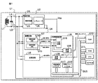
図1は、本発明の実施の形態による非接触ICカードの基本的な構成を示す図である。
《Basic configuration of contactless IC card》
FIG. 1 is a diagram showing a basic configuration of a contactless IC card according to an embodiment of the present invention.
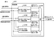
図1に示す非接触ICカードU1は、アンテナL1、共振容量C1、半導体集積回路U2を含んでいる。アンテナL1の一端と共振容量C1の一端とは半導体集積回路U2の第1アンテナ接続端子LAに接続され、アンテナL1の他端と共振容量C1の他端とは半導体集積回路U2の第2アンテナ接続端子LBに接続されている。従って、非接触リーダー/ライター装置からのRFキャリア信号はアンテナ接続端子LA、LBを介して、非接触ICカードU1の動作エネルギーとして電源回路U3に供給されることができる。 A non-contact IC card U1 shown in FIG. 1 includes an antenna L1, a resonance capacitor C1, and a semiconductor integrated circuit U2. One end of the antenna L1 and one end of the resonance capacitor C1 are connected to the first antenna connection terminal LA of the semiconductor integrated circuit U2, and the other end of the antenna L1 and the other end of the resonance capacitor C1 are connected to the second antenna of the semiconductor integrated circuit U2. It is connected to the terminal LB. Therefore, the RF carrier signal from the non-contact reader / writer device can be supplied to the power supply circuit U3 as the operating energy of the non-contact IC card U1 via the antenna connection terminals LA and LB.
また、非接触リーダー/ライター装置からの受信信号は非接触ICカードU1のアンテナ接続端子LA、LBを介して復調回路U7に供給される一方、非接触ICカードU1の変調回路U8からの送信信号はアンテナ接続端子LA、LBとアンテナL1と共振容量C1を介して非接触リーダー/ライター装置に供給されることができる。 The reception signal from the non-contact reader / writer device is supplied to the demodulation circuit U7 via the antenna connection terminals LA and LB of the non-contact IC card U1, while the transmission signal from the modulation circuit U8 of the non-contact IC card U1. Can be supplied to the non-contact reader / writer device via the antenna connection terminals LA and LB, the antenna L1, and the resonance capacitor C1.
半導体集積回路U2は、電源回路U3、内部回路U4を含み、電源回路U3は整流回路U5、レギュレータU6を含み、内部回路U4は復調回路U7、変調回路U8、非接触制御回路U9を含んでいる。復調回路U7は、非接触リーダー/ライター装置からのISO/IEC14443のタイプAの受信信号を受信するための低感度復調回路U14と、非接触リーダー/ライター装置からのISO/IEC14443のタイプBおよびISO/IEC18092の受信信号を受信するための高感度復調回路U15を含んでいる。非接触制御回路U9は、判定回路U16、判定結果レジスタU17、受信エラーレジスタU18、受信回路U19、送信回路U20を含んでいる。非接触制御回路U9には、バス(BUS)を介してRAM(U10)、ROM(U11)、CPU(U12)、EEPROM(U13)および図示はされないが暗号処理等を行うコプロセッサ、インターフェース回路等が接続されている。 The semiconductor integrated circuit U2 includes a power supply circuit U3 and an internal circuit U4. The power supply circuit U3 includes a rectifier circuit U5 and a regulator U6. The internal circuit U4 includes a demodulation circuit U7, a modulation circuit U8, and a non-contact control circuit U9. . The demodulating circuit U7 includes a low-sensitivity demodulating circuit U14 for receiving ISO / IEC14443 type A received signals from the non-contact reader / writer device, and ISO / IEC14443 types B and ISO from the non-contact reader / writer device. A high-sensitivity demodulation circuit U15 for receiving a reception signal of / IEC18092 is included. The non-contact control circuit U9 includes a determination circuit U16, a determination result register U17, a reception error register U18, a reception circuit U19, and a transmission circuit U20. The non-contact control circuit U9 includes a RAM (U10), a ROM (U11), a CPU (U12), an EEPROM (U13) via a bus (BUS), a coprocessor that performs cryptographic processing (not shown), an interface circuit, etc. Is connected.
図1に示す非接触ICカードU1は非接触リーダー/ライター装置からの受信信号がISO/IEC14443のタイプAと、ISO/IEC14443のタイプBと、ISO/IEC18092のいずれの情報伝達方式であるかを、ASK変調度と論理値の時間幅とから検出する機能を有する。 The contactless IC card U1 shown in FIG. 1 indicates which information transmission method is ISO / IEC14443 type A, ISO / IEC14443 type B, or ISO / IEC18092 information received from the contactless reader / writer device. , And a function of detecting from the ASK modulation degree and the time width of the logical value.
図1に示す非接触ICカードU1が非接触リーダー/ライター装置のRFリャリア信号を受信できる動作フィールドに入ると、非接触ICカードU1の電源回路U3の整流回路U5とレギュレータU6とは内部電源電圧VDDを生成して内部回路U4に含まれる各回路へ動作電源電圧として供給する。まず、アンテナL1の両端で受信された受信信号は初期受信の間に復調回路U7の低感度復調回路U14と高感度復調回路U15に供給される一方、低感度復調回路U14の出力と高感度復調回路U15の出力は非接触制御回路U9の判定回路U16に供給される。それによって、現在の受信信号が、タイプAとタイプBと18092とのいずれの情報伝達方式であるかが検出される。最初に、低感度復調回路U14の出力と高感度復調回路U15の出力とは非接触制御回路U9の判定回路U16に供給されることによって、初期受信の間に受信された受信信号のASK変調度が判定回路U16によって検出される。 When the contactless IC card U1 shown in FIG. 1 enters an operation field in which the RF carrier signal of the contactless reader / writer device can be received, the rectifier circuit U5 and the regulator U6 of the power supply circuit U3 of the contactless IC card U1 are connected to the internal power supply voltage. V DD is generated and supplied as an operation power supply voltage to each circuit included in the internal circuit U4. First, received signals received at both ends of the antenna L1 are supplied to the low sensitivity demodulation circuit U14 and the high sensitivity demodulation circuit U15 of the demodulation circuit U7 during the initial reception, while the output of the low sensitivity demodulation circuit U14 and the high sensitivity demodulation are provided. The output of the circuit U15 is supplied to the determination circuit U16 of the non-contact control circuit U9. As a result, it is detected which information transmission method is the type A, type B, or 18092 for the current received signal. First, the output of the low-sensitivity demodulation circuit U14 and the output of the high-sensitivity demodulation circuit U15 are supplied to the determination circuit U16 of the non-contact control circuit U9, so that the ASK modulation degree of the received signal received during the initial reception. Is detected by the determination circuit U16.
後に詳述するように、初期受信の間に復調回路U7の低感度復調回路U14はISO/IEC14443のタイプAのASK変調度が100%の受信信号を検出する一方、復調回路U7の高感度復調回路U15はISO/IEC14443のタイプBおよびISO/IEC18092でASK変調度が10%の受信信号を検出するものである。非接触制御回路U9の判定回路U16は、現在の受信信号のASK変調度は低感度復調回路U14が検出する100%なのか高感度復調回路U15が検出する10%なのかを判定する。例えば、判定回路U16が現在の受信信号のASK変調度は低感度復調回路U14の100%であると判定した場合は、低消費電力モード信号によって高感度復調回路U15の動作が停止される。それによって、初期受信の後の受信ユーザーデータの受信処理の間の高感度復調回路U15の無駄な動作による消費電力が削減できる。逆に、判定回路U16が現在の受信信号のASK変調度は高感度復調回路U15の10%であると判定した場合は、低消費電力モード信号によって低感度復調回路U14の動作が停止される。それによって、初期受信の後の受信ユーザーデータの受信処理の間の低感度復調回路U14の無駄な動作による消費電力が削減できる。 As will be described in detail later, during the initial reception, the low-sensitivity demodulation circuit U14 of the demodulation circuit U7 detects a received signal having an ASK modulation degree of 100% of ISO / IEC14443 type A, while the high-sensitivity demodulation of the demodulation circuit U7. The circuit U15 detects a received signal having an ASK modulation degree of 10% in ISO / IEC14443 type B and ISO / IEC18092. The determination circuit U16 of the non-contact control circuit U9 determines whether the current ASK modulation degree of the received signal is 100% detected by the low sensitivity demodulation circuit U14 or 10% detected by the high sensitivity demodulation circuit U15. For example, when the determination circuit U16 determines that the current ASK modulation degree of the received signal is 100% of that of the low sensitivity demodulation circuit U14, the operation of the high sensitivity demodulation circuit U15 is stopped by the low power consumption mode signal. Thereby, the power consumption due to the useless operation of the high sensitivity demodulation circuit U15 during the reception process of the received user data after the initial reception can be reduced. On the other hand, when the determination circuit U16 determines that the ASK modulation degree of the current received signal is 10% of that of the high sensitivity demodulation circuit U15, the operation of the low sensitivity demodulation circuit U14 is stopped by the low power consumption mode signal. Thereby, power consumption due to useless operation of the low-sensitivity demodulation circuit U14 during reception processing of received user data after initial reception can be reduced.
《ASK変調度の検出》
図2は、ISO/IEC14443のタイプAのASK変調度が100%の場合と、ISO/IEC14443のタイプBおよびISO/IEC18092でASK変調度が10%の場合の非接触ICカードでの非接触リーダー/ライター装置からの受信信号の波形を示す図である。すなわち、図2(A)はISO/IEC14443のタイプAのASK変調度が100%の場合の受信信号の波形であり、図2(B)はISO/IEC14443のタイプBおよびISO/IEC18092でASK変調度が10%の場合の受信信号の波形である。振幅変調された受信信号の最小振幅値aと最大振幅値bとすると、ASK変調度は|b−a|/|b+a|で与えられる。
<< Detection of ASK modulation degree >>
FIG. 2 shows a contactless reader in a contactless IC card when the ASK modulation degree of Type A of ISO / IEC14443 is 100%, and when the ASK modulation degree of ISO / IEC14443 is Type B and ISO / IEC18092 is 10%. FIG. 4 is a diagram showing a waveform of a received signal from a writer device. That is, FIG. 2 (A) shows the waveform of the received signal when the ASK modulation degree of ISO / IEC14443 type A is 100%, and FIG. 2 (B) is the ASK modulation by ISO / IEC14443 type B and ISO / IEC18092. It is a waveform of a received signal when the degree is 10%. Assuming that the minimum amplitude value a and the maximum amplitude value b of the amplitude-modulated received signal are given, the ASK modulation degree is given by | b−a | / | b + a |.
図1に示す非接触ICカードU1の内部回路U4の復調回路U7は、低感度復調回路U14と高感度復調回路U15とを含んでいる。例えば、低感度復調回路U14は、最小振幅値aと最大振幅値bの振幅差が90%以上の振幅差でなければ検出できない低い検出感度を持ち、高感度復調回路U15は、最小振幅値aと最大振幅値bの振幅差が18%以上の振幅差であれば検出できる高い検出感度を持つ。 The demodulation circuit U7 of the internal circuit U4 of the non-contact IC card U1 shown in FIG. 1 includes a low sensitivity demodulation circuit U14 and a high sensitivity demodulation circuit U15. For example, the low sensitivity demodulation circuit U14 has low detection sensitivity that cannot be detected unless the amplitude difference between the minimum amplitude value a and the maximum amplitude value b is 90% or more, and the high sensitivity demodulation circuit U15 has the minimum amplitude value a. And the maximum amplitude value b has a high detection sensitivity that can be detected if the amplitude difference is 18% or more.
図1の復調回路U7の低感度復調回路U14の差動入力端子と高感度復調回路U15の差動入力端子とにアンテナL1の両端の受信信号が供給され、低感度復調回路U14の出力からは2値化信号Aが生成され、高感度復調回路U15の出力からは2値化信号Bが生成される。 The reception signals at both ends of the antenna L1 are supplied to the differential input terminal of the low sensitivity demodulation circuit U14 and the differential input terminal of the high sensitivity demodulation circuit U15 of the demodulation circuit U7 in FIG. A binarized signal A is generated, and a binarized signal B is generated from the output of the high sensitivity demodulation circuit U15.
図2(A)の下には、ISO/IEC14443のタイプAの受信信号に応答する低い検出感度を持つ低感度復調回路U14の出力の2値化信号Aと高い検出感度を持つ高感度復調回路U15の出力の2値化信号Bとが示されている。この場合には、両出力の波形は同一となる。 Below FIG. 2A is a high-sensitivity demodulator circuit having a high detection sensitivity and a binary signal A output from the low-sensitivity demodulator circuit U14 having a low detection sensitivity in response to a type A received signal of ISO / IEC14443. A binary signal B output from U15 is shown. In this case, the waveforms of both outputs are the same.
図2(B)の下には、ISO/IEC14443のタイプBまたはISO/IEC18092の受信信号に応答する低い検出感度の低感度復調回路U14の出力の2値化信号Aと高い検出感度の高感度復調回路U15の出力の2値化信号Bとが示されている。この場合には、高い検出感度の高感度復調回路U15の出力の2値化信号Bからは、ASK変調度が10%のISO/IEC14443のタイプBとISO/IEC18092との受信信号の検出信号が生成される。しかし、低い検出感度の低感度復調回路U14の出力2値化信号Aからは、ASK変調度が10%のISO/IEC14443のタイプBとISO/IEC18092との受信信号の検出信号は生成されない。 Below FIG. 2 (B) is a binary signal A output from the low-sensitivity demodulation circuit U14 with low detection sensitivity in response to a received signal of type B of ISO / IEC14443 or ISO / IEC18092, and high sensitivity with high detection sensitivity. The binarized signal B output from the demodulating circuit U15 is shown. In this case, the detection signal of the received signal of ISO / IEC14443 type B and ISO / IEC18092 having an ASK modulation degree of 10% is obtained from the binary signal B output from the high-sensitivity demodulation circuit U15 having high detection sensitivity. Generated. However, from the output binary signal A of the low-sensitivity demodulation circuit U14 with low detection sensitivity, detection signals of reception signals of ISO / IEC14443 type B and ISO / IEC18092 with an ASK modulation degree of 10% are not generated.
《情報伝達方式の検出》
始めに、非接触リーダー/ライター装置から非接触ICカードU1に送信されるデータを「ダウンリンクデータ」と定義する一方、非接触ICカードU1から非接触リーダー/ライター装置に送信されるデータを「アップリンクデータ」と定義する。
<Detection of information transmission method>
First, data transmitted from the contactless reader / writer device to the contactless IC card U1 is defined as “downlink data”, while data transmitted from the contactless IC card U1 to the contactless reader / writer device is “ It is defined as “uplink data”.
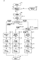
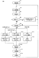
図7は、図1に示す非接触ICカードU1が非接触リーダー/ライター装置からの受信信号がタイプAとタイプBと18092とのいずれの情報伝達方式であるかを検出する動作フローを説明するための図である。 FIG. 7 illustrates an operation flow in which the non-contact IC card U1 shown in FIG. 1 detects which information transmission method is a type A, type B, or 18092 signal received from the non-contact reader / writer device. FIG.
図7のステップF1で図1に示す非接触ICカードU1が非接触リーダー/ライター装置の動作フィールドに入ると、非接触ICカードU1の電源回路U3は内部電源VDDを生成して内部回路U4へ動作電源電圧として供給する。 When the contactless IC card U1 shown in FIG. 1 enters the operation field of the contactless reader / writer device in step F1 of FIG. 7, the power supply circuit U3 of the contactless IC card U1 generates an internal power supply V DD to generate the internal circuit U4. Is supplied as an operating power supply voltage.
次に図7のステップF2で、CPU(U12)はバス(BUS)を介して、非接触制御回路U9内部の判定結果レジスタU17の内容を読み出す。以前に情報伝達方式と情報通信速度との判定が実行されていれば、判定結果レジスタU17には判定回路U16で判定された情報伝達方式と情報通信速度との判定結果の情報とが格納されている。ここでは、以前に判定が実行されていないので、判定結果レジスタU17には判定結果が格納されていないので、非接触ICカードU1の状態は図7のステップF4の初期受信モードに遷移する。すると、図7の次のステップF4−1の初期受信期間に、非接触ICカードU1の復調回路U7での低感度復調回路U14と高感度復調回路U15とによる並列復調動作が実行される。低感度復調回路U14の出力の2値化信号Aと高い検出感度を持つ高感度復調回路U15の出力の2値化信号Bは、判定回路U16に供給される。 Next, in step F2 in FIG. 7, the CPU (U12) reads the contents of the determination result register U17 in the non-contact control circuit U9 via the bus (BUS). If the determination of the information transmission method and the information communication speed has been executed previously, the determination result register U17 stores the information transmission method determined by the determination circuit U16 and the information of the determination result of the information communication speed. Yes. Here, since the determination has not been executed before, the determination result is not stored in the determination result register U17. Therefore, the state of the non-contact IC card U1 shifts to the initial reception mode of step F4 in FIG. Then, in the initial reception period of the next step F4-1 in FIG. 7, the parallel demodulation operation by the low sensitivity demodulation circuit U14 and the high sensitivity demodulation circuit U15 in the demodulation circuit U7 of the non-contact IC card U1 is executed. The binary signal A output from the low-sensitivity demodulation circuit U14 and the binary signal B output from the high-sensitivity demodulation circuit U15 having high detection sensitivity are supplied to the determination circuit U16.
図2(A)の下で説明したように、ISO/IEC14443のタイプAの受信信号を受信する場合には、低感度復調回路U14の出力の2値化信号Aと高感度復調回路U15の出力の2値化信号Bの両出力の波形は同一となる。従って、判定回路U16は、図7のステップF4−2の左側の結果とステップF4−4での方式決定に示すように、同一の波形から現在ASK変調度が100%のISO/IEC14443のタイプAの受信信号を受信していることを判定することができる。そして、判定回路U16は図7の次のステップF4−7でタイプAの受信の判定結果を判定結果レジスタU17に書き込み、図7の更に次のステップF4−10でタイプAの受信ユーザーデータの受信処理を行うものである。この時には、非接触リーダー/ライター装置から非接触ICカードU1への情報伝達方式がISO/IEC14443のタイプAと判定されているので、受信回路U19によってシリアル・パラレル変換された2値化信号の受信ユーザーデータ部分が受信パラレル・データの形態でRAM(U10)に転送されて格納される。受信パラレル・データは、低消費電力状態とされるCPU(U12)とは独立に受信回路U19からの専用信号線を介して例えば1バイト毎にRAM(U10)へ供給される。RAM(U10)には、例えば、固定アドレス(例えば、RAMのメモリ空間の先頭アドレス)から転送されたデータを順次格納することで、データ転送制御に関係する回路規模を抑制することが可能となる。 As described below with reference to FIG. 2A, when receiving a type A reception signal of ISO / IEC14443, the binarized signal A output from the low sensitivity demodulation circuit U14 and the output from the high sensitivity demodulation circuit U15. The waveforms of both outputs of the binarized signal B are the same. Therefore, as shown in the result on the left side of Step F4-2 in FIG. 7 and the method determination in Step F4-4, the determination circuit U16 uses ISO / IEC14443 type A with 100% current ASK modulation degree from the same waveform. It can be determined that the received signal is received. Then, the determination circuit U16 writes the type A reception determination result to the determination result register U17 in the next step F4-7 in FIG. 7, and further receives the type A reception user data in the next step F4-10 in FIG. The processing is performed. At this time, since the information transmission method from the non-contact reader / writer device to the non-contact IC card U1 is determined to be type A of ISO / IEC14443, the reception of the binary signal serial / parallel converted by the reception circuit U19 is received. The user data portion is transferred to and stored in the RAM (U10) in the form of received parallel data. The received parallel data is supplied to the RAM (U10), for example, byte by byte via the dedicated signal line from the receiving circuit U19 independently of the CPU (U12) in the low power consumption state. In the RAM (U10), for example, by sequentially storing data transferred from a fixed address (for example, the start address of the RAM memory space), the circuit scale related to data transfer control can be suppressed. .
ステップF5で受信を終了した後、CPU(U12)は低消費電力状態から動作状態に復帰して、例えば、ROM(U11)またはEEPROM(U13)に格納されたセキュア電子決済処理プログラムに従ってRAM(U10)の格納データを処理して、その処理結果を再びRAM(U10)に格納する。RAM(U10)に格納された処理結果は送信パラレル・データとして非接触制御回路U9の送信回路U20に転送されて、送信回路U20でISO/IEC14443のフレームに変換される。シリアルデータの2値化信号Cは、変調回路U8を介して非接触リーダー/ライター装置へ送信される。 After completing the reception in step F5, the CPU (U12) returns from the low power consumption state to the operating state, and, for example, according to the secure electronic settlement processing program stored in the ROM (U11) or the EEPROM (U13), the RAM (U10). ) Is processed, and the processing result is stored again in the RAM (U10). The processing result stored in the RAM (U10) is transferred as transmission parallel data to the transmission circuit U20 of the non-contact control circuit U9 and converted into an ISO / IEC14443 frame by the transmission circuit U20. The binarized signal C of serial data is transmitted to the non-contact reader / writer device via the modulation circuit U8.
図7のステップF4−10の受信処理中に何らかの受信エラーがあった場合には、図7のステップF4−13で受信回路U19は受信エラーの結果を受信エラーレジスタU18に書き込んで、図7の次のステップF5で受信終了となる。図7のステップF4−10の受信中に受信エラーが発生せず、正常に受信が行われた場合には、ステップF4−13の受信エラーレジスタ設定は不要となって、ステップF5の受信動作終了となる。 If there is any reception error during the reception process in step F4-10 in FIG. 7, the reception circuit U19 writes the result of the reception error in the reception error register U18 in step F4-13 in FIG. In the next step F5, reception ends. If a reception error does not occur during reception in step F4-10 in FIG. 7 and reception is performed normally, the reception error register setting in step F4-13 is not necessary, and the reception operation in step F5 is completed. It becomes.
図2(B)の下で説明したように、ISO/IEC14443のタイプBまたはISO/IEC18092の受信信号を受信する場合には、高感度復調回路U15の出力からはハイレベルとローレベルとの間で変化するASK変調度が10%のISO/IEC14443のタイプBもしくはISO/IEC18092の受信信号の検出信号が2値化信号Bとして生成されることができる。しかし、この場合には、低感度復調回路U14の出力からはハイレベルとローレベルとの間で変化する2値化信号Aが生成されることはできない。従って、判定回路U16は図7のステップF4−2の右側の結果に示すように2値化信号Aと2値化信号Bとの波形の相違から現在ASK変調度が10%のISO/IEC14443のタイプBもしくはISO/IEC18092のいずれかの受信信号を受信していることを判定することができる。 As described below with reference to FIG. 2B, when receiving a reception signal of ISO / IEC14443 type B or ISO / IEC18092, the output of the high-sensitivity demodulation circuit U15 is between the high level and the low level. The detection signal of the received signal of ISO / IEC14443 type B or ISO / IEC18092 whose ASK modulation degree that changes in 10% is 10% can be generated as the binarized signal B. However, in this case, the binarized signal A that changes between the high level and the low level cannot be generated from the output of the low sensitivity demodulation circuit U14. Therefore, as shown in the result on the right side of step F4-2 in FIG. 7, the determination circuit U16 is based on ISO / IEC14443 having a current ASK modulation degree of 10% due to the difference in waveform between the binary signal A and the binary signal B. It can be determined that a reception signal of either type B or ISO / IEC18092 is received.
《2値化信号のパルス幅判定》
現在受信している受信信号がISO/IEC14443のタイプBなのかISO/IEC18092なのかは、判定回路U16による図7のステップF4−3の2値化信号Bのパルス幅判定によって判断することが可能である。
<< Pulse width of binarized signal >>
Whether the currently received signal is ISO / IEC14443 type B or ISO / IEC18092 can be determined by determining the pulse width of the binarized signal B in step F4-3 in FIG. 7 by the determination circuit U16. It is.
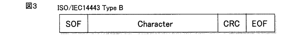
上記非特許文献2に記載されているようにISO/IEC14443のタイプBの非接触リーダー/ライター装置から非接触ICカードU1への送信データとしてのフレームの先頭には、所定の長さの論理“0”を含むSOF(Start Of Frame)が付加されている。
As described in
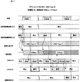
図3は、ISO/IEC14443のタイプBの送信データとしてのフレームの構成を示す図である。図3に示すように、フレームの先頭には通信開始信号としてのSOF(Start Of Frame)が含まれている。フレームの中央には転送ユーザーデータとしてのキャラクター(Character)が含まれ、それに続いて巡回冗長チェックコード(CRC)と通信終了信号としてのEOF(End Of Frame)とが付加されている。 FIG. 3 is a diagram showing the structure of a frame as transmission data of type B of ISO / IEC14443. As shown in FIG. 3, an SOF (Start Of Frame) as a communication start signal is included at the head of the frame. A character (Character) as transfer user data is included in the center of the frame, followed by a cyclic redundancy check code (CRC) and an EOF (End Of Frame) as a communication end signal.
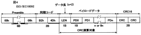
それに対して、上記非特許文献3に記載のように、ISO/IEC18092の非接触リーダー/ライター装置から非接触ICカードU1への送信データパケットの先頭には最小48ビットのエンコードされた論理“0”を含むプリアンブル(Preamble)が通信開始信号として付加されている。
On the other hand, as described in
図4は、ISO/IEC18092の送信データパケットの構成を示す図である。図4に示すように送信データパケットは、先頭からプリアンブル(Preamble)、同期コード、データ長(LEN)、ペイロードデータ(PD0、PD1…PDn)、巡回冗長チェックコード(CRC)を含んでいる。 FIG. 4 is a diagram showing the configuration of a transmission data packet of ISO / IEC18092. As shown in FIG. 4, the transmission data packet includes a preamble (Preamble), a synchronization code, a data length (LEN), payload data (PD0, PD1,... PDn), and a cyclic redundancy check code (CRC) from the beginning.
図5は、非接触リーダー/ライター装置から非接触ICカードU1へのISO/IEC14443のタイプBの送信データの通信速度が106kbps、212kbps、424kbps、848kbpsのそれぞれの場合のフレームの先頭の通信開始信号SOFの時間の長さを示す図である。上記非特許文献2に記載のように、ISO/IEC14443のタイプBのSOFは10〜11etuの論理“0”と2〜3etuの論理“1”とを含むものである。従って、通信速度が比較的低速の212kbpsの場合には10〜11etuの論理“0”の変調期間(変調時間)は47.17〜51.89μSとなり、通信速度が高速の848kbpsの場合には10〜11etuの論理“0”の変調期間は11.79〜12.97μSとなる。尚、etuは、elementary time unitの略である。
FIG. 5 shows a communication start signal at the beginning of a frame when the communication speed of ISO / IEC14443 Type B transmission data from the non-contact reader / writer device to the non-contact IC card U1 is 106 kbps, 212 kbps, 424 kbps, and 848 kbps. It is a figure which shows the length of time of SOF. As described in
図6は、非接触リーダー/ライター装置から非接触ICカードU1へのISO/IEC18092の送信データの通信速度が212kbps、424kbps、848kbpsのそれぞれの場合の送信データパケットの先頭のプリアンブル(Preamble)の論理“0”の時間の長さを示す図である。上記非特許文献3に記載のように、ISO/IEC18092のプリアンブルは最小48ビットのエンコードされた論理“0”を含むものである。従って、通信速度が比較的低速の212kbpsの場合にはプリアンブルの最初の論理“0”の変調期間は2.36μSとなり、通信速度が高速の848kbpsの場合にはプリアンブルの最初の論理“0”の変調期間は0.59μSとなる。
FIG. 6 shows the logic of the preamble of the beginning of the transmission data packet when the communication speed of the transmission data of ISO / IEC18092 from the non-contact reader / writer device to the non-contact IC card U1 is 212 kbps, 424 kbps, and 848 kbps. It is a figure which shows the length of time of "0". As described in
従って、比較的低速の212kbpsの通信速度でのISO/IEC14443のタイプBの送信データのSOFでの論理“0”の変調期間47.17〜51.89μSと比較すると、同一の通信速度でのISO/IEC18092の送信データのプリアンブルの最初の論理“0”の変調期間2.36μSは極めて短い時間となる。この論理“0”のパルス幅の差を判定回路U16が図7のステップF4−3の2値化信号Bのパルス幅判定によって判断することによって、現在受信中の受信信号がISO/IEC14443のタイプBなのかISO/IEC18092なのかの判断が可能となる。 Therefore, compared with the modulation period 47.17 to 51.89 μS of the logic “0” in the SOF of the transmission data of ISO / IEC14443 type B at a relatively low communication speed of 212 kbps, the ISO at the same communication speed The modulation period 2.36 μS of the first logic “0” of the preamble of transmission data of / IEC18092 is an extremely short time. The determination circuit U16 determines the difference between the pulse widths of the logic “0” by determining the pulse width of the binarized signal B in step F4-3 in FIG. 7, so that the received signal currently being received is of the ISO / IEC14443 type. Whether it is B or ISO / IEC18092 can be determined.
従って、図7のステップF4−3の2値化信号Bのパルス幅判定によってその時点での例えば比較的低速の212kbpsの通信速度での論理“0”の変調期間が長いと判定されると、判定回路U16はステップF4−3の左側の結果とステップF4−5に示すように現在ISO/IEC14443のタイプBの受信信号の受信中と通信速度の判定が可能となる。そして、判定回路U16は図7の次のステップF4−8でタイプBの受信の判定結果を判定結果レジスタU17に書き込み、図7の更に次のステップF4−11でタイプBの受信ユーザーデータの受信処理を行うものである。この時には、非接触リーダー/ライター装置から非接触ICカードU1への情報伝達方式がISO/IEC14443のタイプBであると判定されているので、受信回路U19によってシリアル・パラレル変換された2値化信号の受信ユーザーデータ部分がRAM(U10)に転送されて格納される。受信パラレル・データは、低消費電力状態とされるCPU(U12)とは独立に受信回路U19からの専用信号線を介して例えば1バイト毎にRAM(U10)へ供給される。RAM(U10)には、例えば、固定アドレス(例えば、RAMのメモリ空間の先頭アドレス)から転送されたデータを順次格納することで、データ転送制御に関係する回路規模を抑制することが可能となる。 Therefore, when it is determined by the pulse width determination of the binarized signal B in step F4-3 of FIG. 7 that the modulation period of logic “0” at the communication speed of 212 kbps at that time is relatively long, for example. The determination circuit U16 can determine the communication speed while receiving a type B reception signal of ISO / IEC14443 as shown in the result on the left side of step F4-3 and step F4-5. Then, the determination circuit U16 writes the type B reception determination result in the determination result register U17 in the next step F4-8 in FIG. 7, and further receives the type B reception user data in the next step F4-11 in FIG. The processing is performed. At this time, since the information transmission method from the non-contact reader / writer device to the non-contact IC card U1 is determined to be type B of ISO / IEC14443, the binarized signal serial / parallel converted by the receiving circuit U19 The received user data portion is transferred to the RAM (U10) and stored. The received parallel data is supplied to the RAM (U10), for example, byte by byte via the dedicated signal line from the receiving circuit U19 independently of the CPU (U12) in the low power consumption state. In the RAM (U10), for example, by sequentially storing data transferred from a fixed address (for example, the start address of the RAM memory space), the circuit scale related to data transfer control can be suppressed. .
CPU(U12)は、例えばROM(U11)またはEEPROM(U13)に格納されたセキュア電子決済処理プログラムに従ってRAM(U10)の格納データを処理して、その処理結果を再びRAM(U10)に格納する。RAM(U10)の処理結果は送信パラレル・データとして非接触制御回路U9の送信回路U20に転送され、送信回路U20でISO/IEC14443のフレームに変換される。シリアルデータの2値化信号Cは、変調回路U8を介して非接触リーダー/ライター装置へ送信される。 The CPU (U12), for example, processes the data stored in the RAM (U10) according to the secure electronic settlement processing program stored in the ROM (U11) or the EEPROM (U13), and stores the processing result in the RAM (U10) again. . The processing result of the RAM (U10) is transferred as transmission parallel data to the transmission circuit U20 of the non-contact control circuit U9, and is converted into an ISO / IEC14443 frame by the transmission circuit U20. The binarized signal C of serial data is transmitted to the non-contact reader / writer device via the modulation circuit U8.
図7のステップF4−11の受信処理中に何らかの受信エラーがあった場合には、図7のステップF4−14で受信回路U19は受信エラーの結果を受信エラーレジスタU18に書き込んで、図7の次のステップF5で受信終了となる。図7のステップF4−11の受信中に受信エラーが発生せず、正常に受信が行われた場合には、ステップF4−14の受信エラーレジスタ設定は不要となって、ステップF5の受信動作終了となる。 If there is any reception error during the reception process in step F4-11 in FIG. 7, the reception circuit U19 writes the reception error result in the reception error register U18 in step F4-14 in FIG. In the next step F5, reception ends. If a reception error does not occur during reception in step F4-11 in FIG. 7 and the reception is performed normally, the reception error register setting in step F4-14 becomes unnecessary, and the reception operation in step F5 is completed. It becomes.
また、図7のステップF4−3の2値化信号Bのパルス幅判定によってその時点での例えば比較的低速の212kbpsの通信速度での論理“0”の変調期間が短いと判定されると、判定回路U16はステップF4−3の下側の結果とステップF4−6に示すように現在ISO/IEC18092の受信信号の受信中と通信速度の判定が可能となる。そして、判定回路U16は図7の次のステップF4−9で18092の受信の判定結果を判定結果レジスタU17に書き込み、図7の更に次のステップF4−12で18092の受信ユーザーデータの受信処理を行うものである。この時には、非接触リーダー/ライター装置から非接触ICカードU1への情報伝達方式が18092であると判定されているので、受信回路U19によってシリアル・パラレル変換された2値化信号の受信ユーザーデータ部分がRAM(U10)に転送されて格納される。受信パラレル・データは、低消費電力状態とされるCPU(U12)とは独立に受信回路U19からの専用信号線を介して例えば1バイト毎にRAM(U10)へ供給される。RAM(U10)には、例えば、固定アドレス(例えば、RAMのメモリ空間の先頭アドレス)から転送されたデータを順次格納することで、データ転送制御に関係する回路規模を抑制することが可能となる。
When it is determined by the pulse width determination of the binarized signal B in step F4-3 in FIG. 7 that the modulation period of logic “0” at a communication speed of, for example, a relatively low speed of 212 kbps at that time is short. The determination circuit U16 can determine the communication speed during reception of the current ISO /
CPU(U12)は、例えばROM(U11)またはEEPROM(U13)に格納されたセキュア電子決済処理プログラムに従ってRAM(U10)の格納データを処理して、その処理結果を再びRAM(U10)に格納する。RAM(U10)の処理結果は送信パラレル・データとして非接触制御回路U9の送信回路U20に転送され、送信回路U20でISO/IEC18092のフレームに変換される。シリアルデータの2値化信号Cは、変調回路U8を介して非接触リーダー/ライター装置へ送信される。 The CPU (U12), for example, processes the data stored in the RAM (U10) according to the secure electronic settlement processing program stored in the ROM (U11) or the EEPROM (U13), and stores the processing result in the RAM (U10) again. . The processing result of the RAM (U10) is transferred as transmission parallel data to the transmission circuit U20 of the non-contact control circuit U9, and is converted into an ISO / IEC18092 frame by the transmission circuit U20. The binarized signal C of serial data is transmitted to the non-contact reader / writer device via the modulation circuit U8.
図7のステップF4−12の受信処理中に何らかの受信エラーがあった場合には、図7のステップF4−15で受信回路U19は受信エラーの結果を受信エラーレジスタU18に書き込んで、図7の次のステップF5で受信終了となる。図7のステップF4−12の受信中に受信エラーが発生せず、正常に受信が行われた場合には、ステップF4−15の受信エラーレジスタ設定は不要となって、ステップF5の受信動作終了となる。 If there is any reception error during the reception process in step F4-12 in FIG. 7, the reception circuit U19 writes the result of the reception error in the reception error register U18 in step F4-15 in FIG. In the next step F5, reception ends. If a reception error does not occur during reception in step F4-12 in FIG. 7 and the reception is performed normally, the reception error register setting in step F4-15 is unnecessary, and the reception operation in step F5 is completed. It becomes.
更に、図7のステップF4−3の2値化信号Bのパルス幅判定により212kbpsの通信速度での論理“0”の変調期間がタイプBもしくは18092で規定された設定時間の範囲外と判定されると、判定回路U16は非接触ICカードU1の動作状態をステップF4−2に戻す処理を実行する。 Further, by the pulse width determination of the binarized signal B in step F4-3 in FIG. 7, the modulation period of logic “0” at the communication speed of 212 kbps is determined to be out of the set time range defined by type B or 18092. Then, the determination circuit U16 executes processing for returning the operation state of the non-contact IC card U1 to Step F4-2.
《初期受信以降の受信動作、受信エラーまたは変調期間の設定範囲外の後の処理》
図7のステップF4−13とステップF4−14とステップF4−15のいずれかでの受信エラーが発生した時には、受信エラーレジスタU18にそのエラー情報が書き込まれて受信終了となる。その後、CPU(U12)は、受信エラーレジスタU18の内容を読み出す。読み出された内容には受信エラーが含まれているため、CPU(U12)は受信エラーレジスタU18の格納内容と判定結果レジスタU17の格納内容とをクリアする。その後、CPU(U12)は、非接触ICカードU1の動作状態を図7のステップF2すなわち図8のステップF4に戻す処理を実行する。また、図7のステップF4−3のパルス幅判定によって論理“0”の変調期間が設定時間の範囲外と判定された後に、非接触制御回路U9は非接触ICカードU1の動作状態を図7のステップF4−1に戻す処理を実行する。
《Receive operation after initial reception, reception error or processing after setting outside the modulation period setting range》
When a reception error occurs in any of Step F4-13, Step F4-14, and Step F4-15 in FIG. 7, the error information is written in the reception error register U18, and the reception ends. Thereafter, the CPU (U12) reads the contents of the reception error register U18. Since the read content includes a reception error, the CPU (U12) clears the content stored in the reception error register U18 and the content stored in the determination result register U17. Thereafter, the CPU (U12) executes processing for returning the operation state of the non-contact IC card U1 to step F2 in FIG. 7, that is, step F4 in FIG. Further, after it is determined by the pulse width determination of step F4-3 in FIG. 7 that the modulation period of logic “0” is out of the set time range, the non-contact control circuit U9 shows the operation state of the non-contact IC card U1 in FIG. The process to return to step F4-1 is executed.
図8は、図1に示す非接触ICカードU1が初期受信で受信エラーが無く、判定結果レジスタU17に情報伝達方式の判定結果が格納され、初期受信以降の受信で情報伝達方式の判定を省略した動作フローを説明するための図である。 FIG. 8 shows that the contactless IC card U1 shown in FIG. 1 has no reception error in the initial reception, the determination result of the information transmission method is stored in the determination result register U17, and the determination of the information transmission method is omitted in the reception after the initial reception. It is a figure for demonstrating the performed operation | movement flow.
図7の動作フローで、受信エラーが無く判定結果レジスタU17に情報伝達方式の判定結果が格納されると、初期受信が終了する。すると、非接触制御回路U9の判定結果レジスタU17には以前の情報伝達方式の判定結果が格納されているので、非接触ICカードU1の動作状態は図8のステップF3の情報伝達方式確定受信モードに遷移して、更に図8のステップF3−1の受信処理が開始される。初期受信で判定された情報伝達方式は、タイプAもしくはタイプBもしくは18092のいずれかである。従って、図8の次のステップF3−2にて判定回路U16は、初期受信で判定された情報伝達方式を判定結果レジスタU17から判定する。初期受信で判定された情報伝達方式がISO/IEC14443のタイプAであったとの判定結果が判定結果レジスタU17に格納されている場合には、図8のステップF3−9の受信処理では以前と同一の方式であるISO/IEC14443のタイプAの受信処理が実行される。図8のステップF3−9の受信処理中に何らかの受信エラーがあった場合には、図8のステップF3−12で受信回路U19は受信エラーの結果を受信エラーレジスタU18に書き込み、図8の次のステップF5で受信終了となる。 In the operation flow of FIG. 7, when there is no reception error and the determination result of the information transmission method is stored in the determination result register U17, the initial reception ends. Then, since the determination result of the previous information transmission method is stored in the determination result register U17 of the non-contact control circuit U9, the operation state of the non-contact IC card U1 is the information transmission method fixed reception mode in step F3 of FIG. Then, the reception process of step F3-1 in FIG. 8 is started. The information transmission method determined in the initial reception is either type A, type B, or 18092. Accordingly, in the next step F3-2 in FIG. 8, the determination circuit U16 determines the information transmission method determined in the initial reception from the determination result register U17. When the determination result that the information transmission method determined in the initial reception is ISO / IEC14443 type A is stored in the determination result register U17, the reception process in step F3-9 in FIG. 8 is the same as before. ISO / IEC14443 type A reception processing is executed. If there is any reception error during the reception process in step F3-9 in FIG. 8, the reception circuit U19 writes the reception error result in the reception error register U18 in step F3-12 in FIG. In step F5, reception ends.
しかし、図8のステップF3−2で判定結果レジスタU17から判定によって初期受信で判定された情報伝達方式がISO/IEC14443のタイプBまたはISO/IEC18092であった時には、図8のステップF3−3とステップF3−4とで2値化信号Bのパルス幅判定が実行される。 However, when the information transmission method determined in the initial reception by the determination from the determination result register U17 in step F3-2 in FIG. 8 is ISO / IEC14443 type B or ISO / IEC18092, step F3-3 in FIG. In step F3-4, the pulse width determination of the binarized signal B is executed.
すなわち、図8のステップF3−3での判定回路U16による2値化信号Bのパルス幅判定によって現在ISO/IEC14443のタイプBの受信信号の受信中と通信速度が判定されると、判定回路U16は図8のステップF3−5で通信速度を決定してステップF3−7でタイプBの受信の判定結果を判定結果レジスタU17に書き込むものである。その後、図8のステップF3−10で図7のステップF4−11と同様にタイプBの受信ユーザーデータの受信処理を行う。図8のステップF3−10の受信処理中に何らかの受信エラーがあった場合には、図8のステップF3−13で受信回路U19は受信エラーの結果を受信エラーレジスタU18に書き込んで、図8の次のステップF5で受信終了となる。 That is, when the communication speed is determined to be during reception of a type B received signal of ISO / IEC14443 by the pulse width determination of the binarized signal B by the determination circuit U16 in step F3-3 in FIG. 8, the determination circuit U16 In FIG. 8, the communication speed is determined in step F3-5, and the determination result of type B reception is written in the determination result register U17 in step F3-7. Thereafter, in step F3-10 in FIG. 8, reception processing of type B received user data is performed in the same manner as in step F4-11 in FIG. If there is any reception error during the reception process in step F3-10 in FIG. 8, the reception circuit U19 writes the result of the reception error in the reception error register U18 in step F3-13 in FIG. In the next step F5, reception ends.
また、図8のステップF3−4での判定回路U16による2値化信号Bのパルス幅判定によって現在ISO/IEC18092の受信信号の受信中と通信速度が判定されると、判定回路U16は図8のステップF3−6で通信速度を決定してステップF3−8で18092の受信の判定結果を判定結果レジスタU17に書き込むものである。その後に、図8のステップF3−11で、図7のステップF4−12と同様に18092の受信ユーザーデータの受信処理を行う。図8のステップF3−11の受信処理中に何らかの受信エラーがあった場合には、図8のステップF3−14で受信回路U19は受信エラーの結果を受信エラーレジスタU18に書き込んで、図8の次のステップF5で受信終了となる。
If the communication speed is determined to be during reception of the received signal of ISO / IEC18092 by the pulse width determination of the binarized signal B by the determination circuit U16 in step F3-4 in FIG. In step F3-6, the communication speed is determined, and in step F3-8, the reception determination result of 18092 is written in the determination result register U17. After that, in step F3-11 in FIG. 8, the reception process for receiving
更に、図8のステップF3−3とステップF3−4とで2値化信号Bのパルス幅判定により論理“0”の変調期間がタイプBもしくは18092で規定された設定時間の範囲外と判定されたとする。つまり、規定された設定期間で定義される通信速度とは異なる通信速度の場合には、判定回路U16は非接触ICカードU1の動作状態をステップF3−2に戻す処理を実行する。その結果、今度は図8のステップF3−3とステップF3−4とのいずれかで、2値化信号Bのパルス幅判定によって論理“0”の変調期間がタイプBもしくは18092で規定された設定時間の範囲内と判定される。すると、判定回路U16はステップF3−5とステップF3−6のいずれかで通信速度を決定して、ステップF3−7とステップF3−8のいずれかで通信速度の判定結果とタイプBもしくは18092の受信の判定結果を判定結果レジスタU17にそれぞれ書き込むものである。その後に、図8のステップF3−10とステップF3−11とのいずれかで、タイプBもしくは18092の受信ユーザーデータの受信を行う。この受信中に何らかの受信エラーがあった場合には、図8のステップF3−13とステップF3−14とのいずれかで受信回路U19は受信エラーの結果を受信エラーレジスタU18に書き込んで、図8の次のステップF5で受信終了となる。 Further, in steps F3-3 and F3-4 in FIG. 8, the modulation period of logic “0” is determined to be out of the set time range defined by type B or 18092 by the pulse width determination of the binarized signal B. Suppose. That is, when the communication speed is different from the communication speed defined in the specified setting period, the determination circuit U16 executes a process for returning the operation state of the non-contact IC card U1 to Step F3-2. As a result, the modulation period of the logic “0” is set by the type B or 18092 by the pulse width determination of the binarized signal B at either step F3-3 or step F3-4 in FIG. Determined to be within the time range. Then, the determination circuit U16 determines the communication speed in either step F3-5 or step F3-6, and determines the communication speed determination result in either step F3-7 or step F3-8 and the type B or 18092. The reception determination result is written in the determination result register U17. Thereafter, reception of user data of type B or 18092 is performed in either step F3-10 or step F3-11 in FIG. If there is any reception error during reception, the reception circuit U19 writes the result of the reception error in the reception error register U18 in either step F3-13 or step F3-14 in FIG. The reception is terminated at the next step F5.
以上説明したように、図7の動作フローと図8の動作フローとによって制御される図1に示す非接触ICカードU1は、一度、タイプA、タイプBもしくは18092のいずれかの情報伝達方式を判定すると、動作フィールド外部への移動によって非接触リーダー/ライター装置からのRFキャリア信号が停止されるまで、または、CPU(U12)によって判定結果レジスタU17に格納された判定結果がクリアされるまで、判定結果レジスタU17に格納された判定結果は保持されている。 As described above, the non-contact IC card U1 shown in FIG. 1 controlled by the operation flow of FIG. 7 and the operation flow of FIG. When the determination is made, until the RF carrier signal from the non-contact reader / writer device is stopped due to the movement outside the operation field or until the determination result stored in the determination result register U17 is cleared by the CPU (U12), The determination result stored in the determination result register U17 is held.
図7のステップF4−13、F4−14、F4−15のいずれかの後のステップF5の受信終了もしくは図8のステップF3−13、F3−14、F3−15のいずれかの後のステップF5の受信終了の後に、図18に示すメモリ領域のアドレス0に格納されている共通プログラムが実行される。 End of reception in step F5 after any of steps F4-13, F4-14, F4-15 in FIG. 7 or step F5 after any of steps F3-13, F3-14, F3-15 in FIG. After the end of reception, the common program stored at address 0 in the memory area shown in FIG. 18 is executed.
図18は、図1に示す非接触ICカードU1のROM(U10)もしくはEEPROM(U13)等の不揮発性メモリに格納されて非接触ICカードU1によって実行される種々のプログラムの構成を示す図である。 18 is a diagram showing the configuration of various programs stored in a non-volatile memory such as ROM (U10) or EEPROM (U13) of contactless IC card U1 shown in FIG. 1 and executed by contactless IC card U1. is there.
図18に示す不揮発性メモリのメモリ領域のアドレス0と、アドレス1と、アドレス2と、アドレス3とには、それぞれ共通プログラムと、ISO/IEC14443のタイプAのためのプログラムと、ISO/IEC14443のタイプBのためのプログラムと、ISO/IEC18092のためのプログラムが格納されている。
The address 0,
CPU(U12)による図18の不揮発性メモリのメモリ領域のアドレス0に格納された共通プログラムの実行によって、図9のステップF6でCPU(U12)は受信エラーレジスタU18の内容を読み出し、受信エラーが有るか否かを確認する。 By execution of the common program stored at address 0 of the memory area of the nonvolatile memory in FIG. 18 by the CPU (U12), the CPU (U12) reads the contents of the reception error register U18 in step F6 in FIG. Check if it exists.
図9は、図1の非接触ICカードU1による図7の動作フローのステップF4の初期受信から受信エラーによるステップF5の受信終了の動作実行の後に実行される動作フローを説明するための図である。 FIG. 9 is a diagram for explaining an operation flow executed from the initial reception at step F4 of the operation flow of FIG. 7 by the non-contact IC card U1 of FIG. 1 to the end of reception at step F5 due to a reception error. is there.
図9のステップF5での受信エラーによる受信終了の後に、ステップF6でCPU(U12)は受信エラーレジスタU18の内容を読み出し、受信エラーが有るか否かを確認する。もし、受信エラーがある場合には、図9のステップF7で受信エラーレジスタU18の格納内容と判定結果レジスタU17の格納内容をクリアした後、再びステップF4の初期受信とステップF4−1の受信開始とが実行される。 After completion of reception due to the reception error in step F5 in FIG. 9, in step F6, the CPU (U12) reads the contents of the reception error register U18 and confirms whether there is a reception error. If there is a reception error, the contents stored in the reception error register U18 and the contents stored in the determination result register U17 are cleared in step F7 in FIG. 9, and then the initial reception in step F4 and the reception start in step F4-1 are started again. Are executed.
同様な処理の反復によって図9のステップF6での受信エラーが無くなるので、図9のステップF8ではCPU(U12)が判定結果レジスタU17の格納内容を読み出して、タイプA、タイプB、18092のいずれかの情報伝達方式が格納されているか否かを確認する。もし、判定結果レジスタU17にいずれの情報伝達方式の結果も格納されていない場合には、ステップF4の初期受信とステップF4−1の受信開始とが実行される。判定結果レジスタU17にいずれかの情報伝達方式の結果が格納されている場合には、図9のステップF9、ステップF10、ステップF11に示すように図18のメモリ領域のアドレス1のタイプA、アドレス2のタイプB、アドレス3の18092のいずれかのプログラムに遷移するものとなる。従って、図9のステップF12、ステップF13、ステップF14に示すように、タイプAとタイプBと18092のいずれかの受信エラーの発生時と同一のプログラムが実行される。
Since the reception error in step F6 in FIG. 9 is eliminated by repeating the same processing, in step F8 in FIG. 9, the CPU (U12) reads the stored contents of the determination result register U17, and any of type A, type B, and 18092 It is confirmed whether the information transmission method is stored. If the result of any information transmission method is not stored in the determination result register U17, the initial reception in step F4 and the reception start in step F4-1 are executed. When the result of one of the information transmission methods is stored in the determination result register U17, as shown in Step F9, Step F10, and Step F11 in FIG. 9, the type A and address of the
ステップF15にてプログラム実行が完了すると、ステップF17にて判定結果レジスタU17に格納されたタイプA、タイプB、18092のいずれかの情報伝達方式によって送信動作を実行して、ステップF18で送信動作を完了する。再び、非接触リーダー/ライター装置からの送信データを受信すると、図9の動作フローを行い、必要なデータ送受信を繰り返す。 When the program execution is completed in step F15, the transmission operation is executed by one of the information transmission methods of type A, type B, and 18092 stored in the determination result register U17 in step F17, and the transmission operation is performed in step F18. Complete. When the transmission data from the non-contact reader / writer device is received again, the operation flow of FIG. 9 is performed and necessary data transmission / reception is repeated.
《非接触ICカードの詳細な構成》
《非接触制御回路の構成》
図10は、図1に示す非接触ICカードU1の半導体集積回路U2の内部回路U4に含まれた非接触制御回路U9の構成を示す図である。
《Detailed configuration of contactless IC card》
《Configuration of non-contact control circuit》
FIG. 10 is a diagram showing a configuration of a non-contact control circuit U9 included in the internal circuit U4 of the semiconductor integrated circuit U2 of the non-contact IC card U1 shown in FIG.
図10に示す非接触制御回路U9は、判定回路U16、判定結果レジスタU17、受信エラーレジスタU18、受信回路U19、送信回路U20、バス(BUS)を含んでいる。図1のように、判定回路U16には、復調回路U7の低感度復調回路U14、高感度復調回路U15の2値化信号A、2値化信号Bが供給され、判定回路U16から復調回路U7へ低消費電力モード信号が供給される。受信回路U19には、復調回路U7の低感度復調回路U14、高感度復調回路U15の2値化信号A、2値化信号Bと判定回路U16の情報通信速度判定信号と情報伝達方式判定信号が供給される。受信回路U19からRAM(U10)へ受信パラレル・データが転送される一方、受信回路U19から受信エラーレジスタ(U18)にエラー検出信号が供給される。判定結果レジスタ(U17)には判定回路U16の情報通信速度判定信号と情報伝達方式判定信号が供給される一方、判定結果レジスタ(U17)から送信回路(U20)には情報通信速度判定信号と情報伝達方式判定信号とが供給される。送信回路(U20)にはRAM(U10)から送信パラレル・データが転送される一方、送信回路(U20)から図1の変調回路U8に2値化信号Cが供給される。 The non-contact control circuit U9 shown in FIG. 10 includes a determination circuit U16, a determination result register U17, a reception error register U18, a reception circuit U19, a transmission circuit U20, and a bus (BUS). As shown in FIG. 1, the determination circuit U16 is supplied with the binary signal A and the binary signal B of the low sensitivity demodulation circuit U14 of the demodulation circuit U7 and the high sensitivity demodulation circuit U15, and from the determination circuit U16 to the demodulation circuit U7. Is supplied with a low power consumption mode signal. The reception circuit U19 includes a low-sensitivity demodulation circuit U14 of the demodulation circuit U7, a binary signal A of the high-sensitivity demodulation circuit U15, a binary signal B, an information communication speed determination signal and an information transmission method determination signal of the determination circuit U16. Supplied. While receiving parallel data is transferred from the receiving circuit U19 to the RAM (U10), an error detection signal is supplied from the receiving circuit U19 to the receiving error register (U18). The determination result register (U17) is supplied with the information communication speed determination signal and the information transmission method determination signal of the determination circuit U16, while the determination result register (U17) sends the information communication speed determination signal and the information to the transmission circuit (U20). A transmission method determination signal is supplied. Transmission parallel data is transferred from the RAM (U10) to the transmission circuit (U20), while a binary signal C is supplied from the transmission circuit (U20) to the modulation circuit U8 in FIG.
《判定回路の構成》
図11は、図1に示す非接触ICカードU1の半導体集積回路U2の内部回路U4の非接触制御回路U9に含まれた判定回路U16の構成を示す図である。
<< Configuration of judgment circuit >>
FIG. 11 is a diagram showing a configuration of the determination circuit U16 included in the non-contact control circuit U9 of the internal circuit U4 of the semiconductor integrated circuit U2 of the non-contact IC card U1 shown in FIG.
図11に示す判定回路U16は、復調回路U7の低感度復調回路U14からの2値化信号Aのローレベルからハイレベルへの変化に応答するエッジ検出回路U21を含んでいる。また判定回路U16は、復調回路U7の高感度復調回路U15からの2値化信号Bが供給されるパルス幅検出器U22を含み、パルス幅検出器U22はパルス幅カウンタU23を含んでいる。 The determination circuit U16 shown in FIG. 11 includes an edge detection circuit U21 that responds to a change from the low level to the high level of the binary signal A from the low sensitivity demodulation circuit U14 of the demodulation circuit U7. The determination circuit U16 includes a pulse width detector U22 to which the binarized signal B from the high sensitivity demodulation circuit U15 of the demodulation circuit U7 is supplied. The pulse width detector U22 includes a pulse width counter U23.
例えば、復調回路U7の低感度復調回路U14がISO/IEC14443のタイプAのASK変調度100%の受信信号を受信する場合には、低感度復調回路U14の2値化信号Aはローレベルからハイレベルに変化する。このレベル変化に応答してエッジ検出回路U21は、タイプAでの受信モードの情報伝達方式判定信号を生成する。この情報伝達方式判定信号は復調回路U7の高感度復調回路U15の動作を停止する低消費電力モード信号となり、またパルス幅検出器U22への動作停止制御信号となる。従って、判定回路U16のエッジ検出回路U21は、図7の動作フローのステップF4−2のASK変調度判定の判定結果を生成するものである。 For example, when the low-sensitivity demodulation circuit U14 of the demodulation circuit U7 receives an ISO / IEC14443 type A received signal of 100% ASK modulation degree, the binary signal A of the low-sensitivity demodulation circuit U14 changes from low level to high. Change to level. In response to this level change, the edge detection circuit U21 generates a type A reception mode information transmission method determination signal. This information transmission method determination signal becomes a low power consumption mode signal for stopping the operation of the high sensitivity demodulation circuit U15 of the demodulation circuit U7, and also becomes an operation stop control signal to the pulse width detector U22. Therefore, the edge detection circuit U21 of the determination circuit U16 generates the determination result of the ASK modulation degree determination in step F4-2 in the operation flow of FIG.
一方、復調回路U7の高感度復調回路U15がISO/IEC14443のタイプBもしくはISO/IEC18092のASK変調度10%の受信信号を受信している場合は、低感度復調回路U14からの2値化信号Aはローレベルに維持されている。従って、現在の受信信号がタイプBと18092とのいずれであるかを判定するために、図7の動作フローのステップF4−3での2値化信号Bパルス幅判定が必要となる。従って、パルス幅検出器U22のパルス幅カウンタU23は、2値化信号Bのパルス幅判定のために論理“0”の変調期間の短長を判定する。すなわちパルス幅カウンタU23は、2値化信号Bの論理“0”の期間にてクロック数をカウントするものである。カウント数が大きな上側の4つのケースは論理“0”の変調期間が長いISO/IEC14443のタイプBの受信信号と判定され、カウント数が小さな下側の3つのケースは論理“0”の変調期間が長いISO/IEC18092の受信信号と判定される。また、これらの7つのケースでは、106kbpsから848kbpsまでの情報通信速度も同時に判定されることができる。また、パルス幅検出器U22は、カウント数とタイプBまたは18092の情報伝達方式および情報通信速度をリンクするルックアップテーブル(参照テーブル)を含むものである。
On the other hand, when the high-sensitivity demodulation circuit U15 of the demodulation circuit U7 receives a reception signal of ISO / IEC14443 type B or ISO / IEC18092
《受信回路の構成》
図12は、図1に示す非接触ICカードU1の半導体集積回路U2の内部回路U4の非接触制御回路U9に含まれた受信回路U19の構成を示す図である。
<Receiver circuit configuration>
FIG. 12 is a diagram showing a configuration of a receiving circuit U19 included in the noncontact control circuit U9 of the internal circuit U4 of the semiconductor integrated circuit U2 of the noncontact IC card U1 shown in FIG.
図12に示す受信回路U19は、タイプAのデータ抽出回路U191とタイプBのデータ抽出回路U192と18092のデータ抽出回路U193と出力セレクターU194を含んでいる。 The reception circuit U19 shown in FIG. 12 includes a type A data extraction circuit U191, a type B data extraction circuit U192, a data extraction circuit U193 of 18092, and an output selector U194.
タイプAのデータ抽出回路U191には復調回路U7の低感度復調回路U14のシリアルの2値化信号Aと判定回路U16の情報伝達方式判定信号が供給され、タイプAのデータ抽出回路U191からはタイプAの受信パラレル・データと受信エラー信号とが生成されて出力セレクターU194に供給される。 The type A data extraction circuit U191 is supplied with the serial binary signal A of the low sensitivity demodulation circuit U14 of the demodulation circuit U7 and the information transmission system determination signal of the determination circuit U16. A reception parallel data of A and a reception error signal are generated and supplied to the output selector U194.
タイプBのデータ抽出回路U192には復調回路U7の高感度復調回路U15のシリアルの2値化信号Bと判定回路U16の情報伝達方式判定信号と情報通信速度判定信号とが供給され、タイプBのデータ抽出回路U192からはタイプBの受信パラレル・データと受信エラー信号とが生成されて出力セレクターU194に供給される。 The type B data extraction circuit U192 is supplied with the serial binarized signal B of the high sensitivity demodulation circuit U15 of the demodulation circuit U7, the information transmission method determination signal and the information communication speed determination signal of the determination circuit U16. From the data extraction circuit U192, type B reception parallel data and a reception error signal are generated and supplied to the output selector U194.
18092のデータ抽出回路U193には復調回路U7の高感度復調回路U15のシリアルの2値化信号Bと判定回路U16の情報伝達方式判定信号と情報通信速度判定信号とが供給され、この18092のデータ抽出回路U193からは18092の受信パラレル・データと受信エラー信号とが生成されて出力セレクターU194に供給される。 The data extraction circuit U193 of 18092 is supplied with the serial binarized signal B of the high-sensitivity demodulation circuit U15 of the demodulation circuit U7, the information transmission method determination signal of the determination circuit U16, and the information communication speed determination signal. From the extraction circuit U193, 18092 reception parallel data and a reception error signal are generated and supplied to the output selector U194.
データ抽出回路U191、データ抽出回路U192、データ抽出回路U193、出力セレクターU194に判定結果レジスタ17から供給される情報伝達方式判定信号は、タイプA、タイプB、18092のいずれかの方式である。従って、情報伝達方式判定信号によって指定された方式に従って、タイプAのデータ抽出回路U191とタイプBのデータ抽出回路U192と18092のデータ抽出回路U193とのいずれかが低消費電力状態または非活性化状態から活性化される。従って、活性化されたデータ抽出回路は、受信シリアル入力信号から受信パラレル・データと受信エラー信号とを生成する。 The information transmission method determination signal supplied from the determination result register 17 to the data extraction circuit U191, the data extraction circuit U192, the data extraction circuit U193, and the output selector U194 is one of type A, type B, and 18092. Therefore, either the type A data extraction circuit U191, the type B data extraction circuit U192, or the 18092 data extraction circuit U193 is in a low power consumption state or an inactive state according to the method specified by the information transmission method determination signal. Activated from. Therefore, the activated data extraction circuit generates reception parallel data and a reception error signal from the reception serial input signal.
出力セレクターU194には判定回路U16からのタイプAとタイプBと18092とのいずれかの情報伝達方式判定信号が供給されているので、出力セレクターU194はこのいずれかの方式の受信パラレル・データとエラー検出信号とを選択して、受信パラレル・データをRAM(U10)に転送して、エラー検出信号を受信エラーレジスタ(U18)に供給するものである。 Since the output selector U194 is supplied with any type A, type B, or 18092 information transmission system determination signal from the determination circuit U16, the output selector U194 receives the received parallel data and error of either system. The detection signal is selected, the received parallel data is transferred to the RAM (U10), and the error detection signal is supplied to the reception error register (U18).
《送信回路の構成》
図13は、図1に示す非接触ICカードU1の半導体集積回路U2の内部回路U4の非接触制御回路U9に含まれた送信回路U20の構成を示す図である。
<< Transmission circuit configuration >>
FIG. 13 is a diagram showing a configuration of the transmission circuit U20 included in the non-contact control circuit U9 of the internal circuit U4 of the semiconductor integrated circuit U2 of the non-contact IC card U1 shown in FIG.
図13に示す送信回路U20は、タイプAのフレーム変換回路U201とタイプBのフレーム変換回路U202と18092のフレーム変換回路U203と出力セレクターU204を含んでいる。 The transmission circuit U20 shown in FIG. 13 includes a type A frame conversion circuit U201, a type B frame conversion circuit U202, a 18092 frame conversion circuit U203, and an output selector U204.
判定結果レジスタ17からの情報伝達方式判定信号はタイプAのフレーム変換回路U201とタイプBのフレーム変換回路U202と18092のフレーム変換回路U203と共通に供給され、判定結果レジスタ17からの情報通信速度判定信号はタイプBのフレーム変換回路U202と18092のフレーム変換回路U203とに供給される。バス(BUS)を介して転送されるRAM(U10)からの送信パラレル・データは、タイプAのフレーム変換回路U201とタイプBのフレーム変換回路U202と18092のフレーム変換回路U203と共通に供給される。 The information transmission method determination signal from the determination result register 17 is supplied in common to the type A frame conversion circuit U201, the type B frame conversion circuit U202, and the 18092 frame conversion circuit U203, and the information communication speed determination from the determination result register 17 is performed. The signal is supplied to a type B frame conversion circuit U202 and a 18092 frame conversion circuit U203. Transmission parallel data from the RAM (U10) transferred via the bus (BUS) is supplied in common to the type A frame conversion circuit U201, the type B frame conversion circuit U202, and the 18092 frame conversion circuit U203. .
フレーム変換回路U201、フレーム変換回路U202、フレーム変換回路U203、出力セレクターU204に判定結果レジスタ17から供給される情報伝達方式判定信号は、タイプAとタイプBと18092とのいずれかの方式である。従って、情報伝達方式判定信号によって指定された方式に従って、タイプAのフレーム変換回路U201とタイプBのフレーム変換回路U202と18092のフレーム変換回路U203とのいずれかが低消費電力状態または非活性化状態から活性化される。従って、活性化された変換回路は、専用信号線を介してRAM(U10)からの送信パラレル・データを判定結果レジスタ17からの情報通信速度判定信号に従って送信シリアルデータに変換する。出力セレクターU204は、情報伝達方式判定信号に従って送信シリアルデータを選択して2値化信号Cを生成して変調回路8に供給する。
The information transmission method determination signal supplied from the determination result register 17 to the frame conversion circuit U201, the frame conversion circuit U202, the frame conversion circuit U203, and the output selector U204 is one of type A, type B, and 18092. Therefore, either the type A frame conversion circuit U201, the type B frame conversion circuit U202, or the 18092 frame conversion circuit U203 is in a low power consumption state or an inactive state according to the method specified by the information transmission method determination signal. Activated from. Therefore, the activated conversion circuit converts the transmission parallel data from the RAM (U10) into transmission serial data according to the information communication speed determination signal from the determination result register 17 via the dedicated signal line. The output selector U204 selects transmission serial data in accordance with the information transmission method determination signal, generates a binary signal C, and supplies it to the
以上説明したように、復調回路U7と判定回路U16と受信回路U19とによるデータの受信動作の間、もしくは、送信回路U20と変調回路U8とによるデータの送信動作の間では、RF信号の復調または変調処理とRAM(U10)とのデータ転送とに直接関係のないCPU(U12)とバス(BUS)とを低消費電力状態にできるので、非接触リーダー/ライター装置とのデータ通信時の消費電力の低減を実現することが可能となる。 As described above, during the data reception operation by the demodulation circuit U7, the determination circuit U16, and the reception circuit U19, or during the data transmission operation by the transmission circuit U20 and the modulation circuit U8, the RF signal demodulation or Since the CPU (U12) and the bus (BUS), which are not directly related to the modulation processing and the data transfer with the RAM (U10), can be brought into a low power consumption state, the power consumption during data communication with the non-contact reader / writer device Can be reduced.
《タイプAの受信》
図14は、図1に示す非接触ICカードU1が非接触リーダー/ライター装置からISO/IEC14443のタイプAの情報伝達方式による受信信号を受信する場合の動作を示す図である。
<Type A reception>
FIG. 14 is a diagram showing an operation when the non-contact IC card U1 shown in FIG. 1 receives a reception signal by the ISO /
図14に示すように非接触ICカードU1が非接触リーダー/ライター装置の動作フィールドに入ると、非接触ICカードU1の復調回路U7での低感度復調回路U14と高感度復調回路U15とによる並列復調動作が実行される。1回目のダウンリンク通信の直前に、判定回路U16は図7のステップF4−2の左側で現在ASK変調度が100%のISO/IEC14443のタイプAの受信信号の受信を判定する。従って、判定回路U16からの低消費電力モード信号によって、高感度復調回路U15の動作が停止される。従って、タイプAの受信ユーザーデータは復調回路U7の低感度復調回路U14と非接触制御回路U9の受信回路U19とによって受信された後に、専用信号線としての受信パラレル・データ信号線を介してRAM(U10)に格納される。 As shown in FIG. 14, when the non-contact IC card U1 enters the operation field of the non-contact reader / writer device, the low-sensitivity demodulation circuit U14 and the high-sensitivity demodulation circuit U15 in the demodulation circuit U7 of the non-contact IC card U1 perform parallel processing. Demodulation is performed. Immediately before the first downlink communication, the determination circuit U16 determines reception of a type A received signal of ISO / IEC14443 having a current ASK modulation degree of 100% on the left side of step F4-2 in FIG. Therefore, the operation of the high sensitivity demodulation circuit U15 is stopped by the low power consumption mode signal from the determination circuit U16. Therefore, the received user data of type A is received by the low-sensitivity demodulation circuit U14 of the demodulation circuit U7 and the reception circuit U19 of the non-contact control circuit U9, and then received via the reception parallel data signal line as a dedicated signal line. (U10).
RAM(U10)への受信ユーザーデータの格納の終了時点での割り込み信号に応答してCPU(U11)は、停止状態からウェーク(起動)して動作状態に移行する。CPU(U11)はRAM(U10)に格納されたデータを読み出して、ROM(U11)またはEEPROM(U13)に格納されたセキュア電子決済処理プログラムに従って読み出しデータを処理して、その処理結果を再びRAM(U10)に格納する。CPU(U11)による処理結果のRAM(U10)への格納の完了時点で、CPU(U11)は動作状態からスリープ状態の停止状態に移行する。 In response to the interrupt signal at the end of storing the received user data in the RAM (U10), the CPU (U11) wakes (starts) from the stopped state and shifts to the operating state. The CPU (U11) reads the data stored in the RAM (U10), processes the read data in accordance with the secure electronic settlement processing program stored in the ROM (U11) or the EEPROM (U13), and returns the processing result to the RAM again. Store in (U10). Upon completion of storing the processing results by the CPU (U11) in the RAM (U10), the CPU (U11) shifts from the operation state to the sleep state stop state.
CPU(U11)の動作状態からスリープ状態への移行に応答して、送信回路(U20)と変調回路(U8)とは停止状態からウェーク(起動)して動作状態に移行する。従って、送信回路(U20)は、RAM(U10)に格納された処理結果を専用信号線としての送信パラレル・データ信号線を介して読み出して、変調回路(U8)へ転送する。その結果、変調回路(U8)による非接触リーダー/ライター装置への1回目のアップリンク通信が実行される。 In response to the transition from the operation state of the CPU (U11) to the sleep state, the transmission circuit (U20) and the modulation circuit (U8) wake (start) from the stop state and shift to the operation state. Accordingly, the transmission circuit (U20) reads out the processing result stored in the RAM (U10) via the transmission parallel data signal line as a dedicated signal line and transfers it to the modulation circuit (U8). As a result, the first uplink communication to the non-contact reader / writer device by the modulation circuit (U8) is executed.
《タイプBの受信》
図15は、図1に示す非接触ICカードU1が非接触リーダー/ライター装置からISO/IEC14443のタイプBの情報伝達方式による受信信号を受信する場合の動作を示す図である。
<Receiving type B>
FIG. 15 is a diagram showing an operation when the non-contact IC card U1 shown in FIG. 1 receives a reception signal by the ISO / IEC14443 type B information transmission method from the non-contact reader / writer device.
図15に示すように非接触ICカードU1が非接触リーダー/ライター装置の動作フィールドに入ると、非接触ICカードU1の復調回路U7での低感度復調回路U14と高感度復調回路U15とによる並列復調動作が実行される。1回目のダウンリンク通信の直前に、判定回路U16は図7のステップF4−2の右側で現在ASK変調度が10%の受信信号の受信を判定している。また判定回路U16は、図7のステップF4−3での2値化信号Bのパルス幅判定によるISO/IEC14443のタイプBもしくはISO/IEC18092の受信信号の受信を判定する。判定回路U16によって論理“0”の変調期間が長いと判定されると、判定回路U16はステップF4−3の左側の結果とステップF4−5に示すように現在ISO/IEC14443のタイプBの受信信号の受信中と106kbpsの情報通信速度の判定を実行し、判定回路U16からの低消費電力モード信号によって低感度復調回路U14の動作が停止される。従って、タイプBの受信ユーザーデータは復調回路U7の高感度復調回路U15と非接触制御回路U9の受信回路U19とによって受信された後に、専用信号線としての受信パラレル・データ信号線を介してRAM(U10)に格納される。 As shown in FIG. 15, when the non-contact IC card U1 enters the operation field of the non-contact reader / writer device, the low-sensitivity demodulation circuit U14 and the high-sensitivity demodulation circuit U15 in the demodulation circuit U7 of the non-contact IC card U1 perform parallel processing. Demodulation is performed. Immediately before the first downlink communication, the determination circuit U16 determines reception of a reception signal having a current ASK modulation degree of 10% on the right side of Step F4-2 in FIG. The determination circuit U16 determines reception of a reception signal of ISO / IEC14443 type B or ISO / IEC18092 based on the pulse width determination of the binarized signal B in step F4-3 in FIG. When the determination circuit U16 determines that the modulation period of logic “0” is long, the determination circuit U16 outputs the result of the left side of step F4-3 and the received signal of the current ISO / IEC14443 type B as shown in step F4-5. And the information communication speed of 106 kbps are determined, and the operation of the low sensitivity demodulation circuit U14 is stopped by the low power consumption mode signal from the determination circuit U16. Accordingly, the received user data of type B is received by the high sensitivity demodulating circuit U15 of the demodulating circuit U7 and the receiving circuit U19 of the non-contact control circuit U9, and then received via the receiving parallel data signal line as a dedicated signal line. (U10).
RAM(U10)への受信ユーザーデータの格納の終了時点での割り込み信号に応答してCPU(U11)は、停止状態からウェーク(起動)して動作状態に移行する。CPU(U11)はRAM(U10)に格納されたデータを読み出して、ROM(U11)またはEEPROM(U13)に格納されたセキュア電子決済処理プログラムに従って読み出しデータを処理して、その処理結果を再びRAM(U10)に格納する。CPU(U11)による処理結果のRAM(U10)への格納の完了時点で、CPU(U11)は動作状態からスリープ状態の停止状態に移行する。 In response to the interrupt signal at the end of storing the received user data in the RAM (U10), the CPU (U11) wakes (starts) from the stopped state and shifts to the operating state. The CPU (U11) reads the data stored in the RAM (U10), processes the read data in accordance with the secure electronic settlement processing program stored in the ROM (U11) or the EEPROM (U13), and returns the processing result to the RAM again. Store in (U10). Upon completion of storing the processing results by the CPU (U11) in the RAM (U10), the CPU (U11) shifts from the operation state to the sleep state stop state.
CPU(U11)の動作状態からスリープ状態への移行に応答して、送信回路(U20)と変調回路(U8)とは停止状態からウェーク(起動)して動作状態に移行する。従って、送信回路(U20)は、RAM(U10)に格納された処理結果を専用信号線としての送信パラレル・データ信号線を介して読み出して、変調回路(U8)へ転送する。その結果、変調回路(U8)による非接触リーダー/ライター装置への1回目のアップリンク通信が実行される。 In response to the transition from the operation state of the CPU (U11) to the sleep state, the transmission circuit (U20) and the modulation circuit (U8) wake (start) from the stop state and shift to the operation state. Accordingly, the transmission circuit (U20) reads out the processing result stored in the RAM (U10) via the transmission parallel data signal line as a dedicated signal line and transfers it to the modulation circuit (U8). As a result, the first uplink communication to the non-contact reader / writer device by the modulation circuit (U8) is executed.
《18092の受信》
図16は、図1に示す非接触ICカードU1が非接触リーダー/ライター装置からISO/IEC18092の情報伝達方式による受信信号を受信する場合の動作を示す図である。
<< Reception of 18092 >>
FIG. 16 is a diagram showing an operation when the non-contact IC card U1 shown in FIG. 1 receives a reception signal by the ISO /
図16に示すように非接触ICカードU1が非接触リーダー/ライター装置の動作フィールドに入ると、非接触ICカードU1の復調回路U7での低感度復調回路U14と高感度復調回路U15とによる並列復調動作が実行される。1回目のダウンリンク通信の直前に、判定回路U16は図7のステップF4−2の右側で現在ASK変調度が10%の受信信号の受信を判定している。また判定回路U16は、図7のステップF4−3での2値化信号Bのパルス幅判定によるISO/IEC14443のタイプBもしくはISO/IEC18092の受信信号の受信を判定する。判定回路U16によって論理“0”の変調期間が短いと判定されると、判定回路U16はステップF4−3の下側の結果とステップF4−6に示すように現在ISO/IEC18092の受信信号の受信中と424kbpsの情報通信速度の判定を実行し、判定回路U16からの低消費電力モード信号によって低感度復調回路U14の動作が停止される。従って、18092の受信ユーザーデータは復調回路U7の高感度復調回路U15と非接触制御回路U9の受信回路U19とによって受信された後に、専用信号線としての受信パラレル・データ信号線を介してRAM(U10)に格納される。
As shown in FIG. 16, when the non-contact IC card U1 enters the operation field of the non-contact reader / writer device, the low-sensitivity demodulation circuit U14 and the high-sensitivity demodulation circuit U15 in the demodulation circuit U7 of the non-contact IC card U1 perform parallel processing. Demodulation is performed. Immediately before the first downlink communication, the determination circuit U16 determines reception of a reception signal having a current ASK modulation degree of 10% on the right side of Step F4-2 in FIG. The determination circuit U16 determines reception of a reception signal of ISO / IEC14443 type B or ISO / IEC18092 based on the pulse width determination of the binarized signal B in step F4-3 in FIG. When the determination circuit U16 determines that the modulation period of logic “0” is short, the determination circuit U16 receives the current ISO / IEC18092 received signal as shown in the lower result of step F4-3 and step F4-6. The medium and 424 kbps information communication speeds are determined, and the operation of the low sensitivity demodulation circuit U14 is stopped by the low power consumption mode signal from the determination circuit U16. Therefore, the received
RAM(U10)への受信ユーザーデータの格納の終了時点での割り込み信号に応答してCPU(U11)は、停止状態からウェーク(起動)して動作状態に移行する。CPU(U11)はRAM(U10)に格納されたデータを読み出して、ROM(U11)またはEEPROM(U13)に格納されたセキュア電子決済処理プログラムに従って読み出しデータを処理して、その処理結果を再びRAM(U10)に格納する。CPU(U11)による処理結果のRAM(U10)への格納の完了時点で、CPU(U11)は動作状態からスリープ状態の停止状態に移行する。 In response to the interrupt signal at the end of storing the received user data in the RAM (U10), the CPU (U11) wakes (starts) from the stopped state and shifts to the operating state. The CPU (U11) reads the data stored in the RAM (U10), processes the read data in accordance with the secure electronic settlement processing program stored in the ROM (U11) or the EEPROM (U13), and returns the processing result to the RAM again. Store in (U10). Upon completion of storing the processing results by the CPU (U11) in the RAM (U10), the CPU (U11) shifts from the operation state to the sleep state stop state.
CPU(U11)の動作状態からスリープ状態への移行に応答して、送信回路(U20)と変調回路(U8)とは停止状態からウェーク(起動)して動作状態に移行する。従って、送信回路(U20)は、RAM(U10)に格納された処理結果を専用信号線としての送信パラレル・データ信号線を介して読み出して、変調回路(U8)へ転送する。その結果、変調回路(U8)による非接触リーダー/ライター装置への1回目のアップリンク通信が実行される。 In response to the transition from the operation state of the CPU (U11) to the sleep state, the transmission circuit (U20) and the modulation circuit (U8) wake (start) from the stop state and shift to the operation state. Accordingly, the transmission circuit (U20) reads out the processing result stored in the RAM (U10) via the transmission parallel data signal line as a dedicated signal line and transfers it to the modulation circuit (U8). As a result, the first uplink communication to the non-contact reader / writer device by the modulation circuit (U8) is executed.
《受信途中での情報通信速度の変更》
図17は、図1に示す非接触ICカードU1が非接触リーダー/ライター装置からISO/IEC14443のタイプBの情報伝達方式による受信信号の受信中に情報通信速度を変更した後に再び同一のタイプBによる受信を実行する場合の動作を示す図である。
<Change of information communication speed during reception>
FIG. 17 shows the same type B again after the information communication speed is changed while the non-contact IC card U1 shown in FIG. 1 receives the reception signal from the non-contact reader / writer device by the ISO / IEC14443 type B information transmission method. It is a figure which shows the operation | movement in the case of performing reception by.
図17の1回目のダウンリンク通信の動作は図15の1回目のダウンリンク通信の動作と同一であるが、図17のN回目のダウンリンク通信の際には非接触リーダー/ライター装置からISO/IEC14443のタイプBの受信信号の情報通信速度が最低速の106kbpsから中低速の212kbpsに変更される。この情報通信速度の変更は、図8のステップF3−3での判定回路U16による2値化信号Bのパルス幅判定によるタイプBの受信信号の通信速度の判定によって検出されることができる。新しく検出された変更後の情報通信速度は判定結果レジスタU17に書き込まれるので、送信回路U20の送信の情報通信速度は中低速の212kbpsに変更される。また、受信回路U19も新しく検出された変更後の情報通信速度に対応して、シリアルの2値化信号Bを受信パラレル・データに変換するものである。また、この情報通信速度の変更は106kbps、212kbps、424kbps、848kbpsのいずれか1個から他の1個に任意に変更することが可能である。
The operation of the first downlink communication in FIG. 17 is the same as the operation of the first downlink communication in FIG. 15. However, in the N-th downlink communication in FIG. /
またISO/IEC14443のタイプBだけではなくISO/IEC18092の方式による受信信号の受信中に、212kbps、424kbps、848kbpsのいずれか1個から他の1個に任意に変更することが可能である。 Further, it is possible to arbitrarily change any one of 212 kbps, 424 kbps, and 848 kbps from one to another during reception of a received signal not only according to ISO / IEC14443 type B but also in ISO / IEC18092.
《非接触ICカードの構造》
図19は、図1に示す非接触ICカードU1の構造を示す図である。
《Non-contact IC card structure》
FIG. 19 is a diagram showing the structure of the non-contact IC card U1 shown in FIG.
図19に示す非接触ICカードU1は、樹脂モールドされるプリント基板によってカードの形態を取っている。外部の非接触リーダー/ライター装置からの電磁波を受けるアンテナは、プリント基板の配線により形成される渦巻き状のコイルによって構成される。1個のICチップで構成された半導体集積回路U2は、プリント基板に実装され、ICチップにアンテナとなるコイルが接続される。 The non-contact IC card U1 shown in FIG. 19 takes the form of a card by a printed circuit board that is resin-molded. An antenna that receives electromagnetic waves from an external non-contact reader / writer device is constituted by a spiral coil formed by wiring on a printed circuit board. The semiconductor integrated circuit U2 formed of one IC chip is mounted on a printed board, and a coil serving as an antenna is connected to the IC chip.
このように、図19の非接触ICカードU1は携帯電話のように電池を持たないものであり、ICカード単体で非接触リーダー/ライター装置の動作フィールドの範囲内でアンテナによって受信されるRF信号の整流・平滑による低駆動能力の動作電圧で動作するものである。 Thus, the non-contact IC card U1 of FIG. 19 does not have a battery like a mobile phone, and the RF signal received by the antenna within the range of the operation field of the non-contact reader / writer device by itself. It operates at an operating voltage with a low driving capability by rectifying and smoothing.
《携帯電話に搭載される非接触ICカード》
図20は、図1に示す非接触ICカードが携帯電話に搭載される様子を示す図である。
《Non-contact IC card mounted on mobile phone》
FIG. 20 is a diagram illustrating a state in which the non-contact IC card illustrated in FIG. 1 is mounted on a mobile phone.
図20に示す非接触ICカードは、図19に示す非接触ICカードと同様にプリント基板の上にICチップとアンテナとが形成されている。しかし、図20の非接触ICカードは、図19の非接触ICカードよりも極めて小さな外形とされることによって、携帯電話に搭載されることが可能となるものである。従って、図20に示す非接触ICカードは、携帯電話に搭載される移動体通信機能を有するその他の半導体集積回路、液晶表示コントローラ・ドライバ等のその他の半導体集積回路と同様に、携帯電話に内蔵される電池の動作電圧で動作することが可能である。この場合も、低消費電力モード信号に応答して各回路を低消費電力状態とすることで、低消費電力化を実現することが可能となる。 The non-contact IC card shown in FIG. 20 has an IC chip and an antenna formed on a printed circuit board as in the non-contact IC card shown in FIG. However, the non-contact IC card shown in FIG. 20 has an extremely smaller external shape than the non-contact IC card shown in FIG. 19, so that it can be mounted on a mobile phone. Therefore, the non-contact IC card shown in FIG. 20 is built in the mobile phone in the same manner as other semiconductor integrated circuits having a mobile communication function mounted on a mobile phone and other semiconductor integrated circuits such as a liquid crystal display controller / driver. It is possible to operate at the operating voltage of the battery being operated. Also in this case, it is possible to realize low power consumption by putting each circuit in a low power consumption state in response to the low power consumption mode signal.
また、図20に示す非接触ICカードは携帯電話に搭載されるばかりではなく、PDA(Personal Digital Assistant)と呼ばれる手帳タイプのパーソナル・コンピュータやノート型パーソナル・コンピュータの携帯情報端末の全般に内蔵されることが可能である。 Further, the non-contact IC card shown in FIG. 20 is not only mounted on a mobile phone, but is also built in a portable information terminal such as a personal computer of a notebook type called a PDA (Personal Digital Assistant) or a notebook personal computer. Is possible.
以上本発明者によってなされた発明を実施形態に基づいて具体的に説明したが、本発明はそれに限定されるものではなく、その要旨を逸脱しない範囲において種々変更可能であることは言うまでもない。 Although the invention made by the present inventor has been specifically described based on the embodiments, it is needless to say that the present invention is not limited thereto and can be variously modified without departing from the gist thereof.
例えば、本発明は非接触型ICカードに限定されるものではなく、接触型の入出力端子の非接触インターフェースと非接触インターフェースとを持つデュアルタイプICカードに適用することもできる。 For example, the present invention is not limited to a non-contact type IC card, but can be applied to a dual type IC card having a non-contact interface and a non-contact interface of contact type input / output terminals.
また、図1の非接触ICカードにおいて半導体集積回路U2はシングルチップ構成に限定されるものではなく、第1チップと第2チップとのマルチ・チップ構成とすることができる。例えば、第1チップは、電源回路U2と復調回路U7と変調回路U8と非接触制御回路U9とを含むものである。また、第2チップは、RAM(U10)、ROM(U11)、CPU(U12)、EEPROM(U13)、バス(BUS)を含むだけでなく、第1チップとの通信のためのインターフェース回路を含むことができる。 Further, in the non-contact IC card of FIG. 1, the semiconductor integrated circuit U2 is not limited to a single chip configuration, but can be a multi-chip configuration of a first chip and a second chip. For example, the first chip includes a power supply circuit U2, a demodulation circuit U7, a modulation circuit U8, and a non-contact control circuit U9. The second chip not only includes a RAM (U10), a ROM (U11), a CPU (U12), an EEPROM (U13), and a bus (BUS), but also includes an interface circuit for communication with the first chip. be able to.
また、図1の半導体集積回路に搭載される受信回路U19または送信回路U20とRAM(U10)との間のデータ転送は、専用信号線としての受信パラレル・データ線または送信パラレル・データ線は専用信号線に限定されるものではなく、CPU(U12)に接続されたバス(BUS) を介してまたはその他の周辺バスを介してデータ転送を行うことも可能である。 In addition, the data transfer between the reception circuit U19 or transmission circuit U20 and the RAM (U10) mounted on the semiconductor integrated circuit of FIG. 1 is dedicated to the reception parallel data line or the transmission parallel data line as a dedicated signal line. The data transfer is not limited to the signal line, and it is also possible to perform data transfer via a bus (BUS) connected to the CPU (U12) or via other peripheral buses.
また、RAM(U10)に対するデータ転送において、RAM(U10)の固定アドレスから順次格納する構成に限定されるものではなく、メモリ制御回路を利用することによって任意のアドレスに格納することも可能である。 In addition, the data transfer to the RAM (U10) is not limited to the configuration in which the RAM (U10) is sequentially stored from the fixed address, and can be stored at an arbitrary address by using a memory control circuit. .
更に本発明はASK方式のディジタル変調方式による通信だけでなく、周波数偏移変調方式(FSK:Frequency Shift Keying)や位相偏移変調方式(PSK:Phase Shift Keying)等によるディジタル変調方式による通信にも適用することが可能である。 Further, the present invention is not only for communication using the ASK digital modulation method, but also for communication using a digital modulation method such as frequency shift keying (FSK) or phase shift keying (PSK). It is possible to apply.
U1 非接触ICカード
L1 アンテナ
LA 第1アンテナ接続端子
LB 第2アンテナ接続端子
C1 共振容量
U2 半導体集積回路
U3 電源回路
U4 内部回路
U5 整流回路
U6 レギュレータ
U7 復調回路
U8 変調回路
U9 非接触制御回路
U10 RAM
U11 ROM
U12 CPU
U13 EEPROM
U14 低感度復調回路
U15 高感度復調回路
U16 判定回路
U17 判定結果レジスタ
U18 受信エラーレジスタ
U19 受信回路
U20 送信回路
U1 Non-contact IC card L1 Antenna LA First antenna connection terminal LB Second antenna connection terminal C1 Resonance capacity U2 Semiconductor integrated circuit U3 Power supply circuit U4 Internal circuit U5 Rectifier circuit U6 Regulator U7 Demodulator circuit U8 Modulation circuit U9 Non-contact control circuit U10 RAM
U11 ROM
U12 CPU
U13 EEPROM
U14 Low-sensitivity demodulation circuit U15 High-sensitivity demodulation circuit U16 Judgment circuit U17 Judgment result register U18 Reception error register U19 Reception circuit U20 Transmission circuit
Claims (18)
前記第1アンテナ接続端子と前記第2アンテナ接続端子との間にはアンテナによって受信されるRF信号が供給可能とされ、前記電源回路は前記RF信号の整流・平滑によって生成する動作電圧を前記復調回路と前記判定回路とに供給可能とされ、
前記復調回路は第1復調回路と第2復調回路とを含み、前記第1アンテナ接続端子と前記第2アンテナ接続端子との間に供給される前記RF信号は前記第1復調回路の入力と前記第2復調回路の入力とに並列に供給可能とされ、
前記第1復調回路は、前記RF信号として第1変調度を持つ第1受信信号を復調することによって第1復調出力信号を生成可能とされ、
前記第2復調回路は、前記RF信号として前記第1変調度と異なる値の第2変調度および第1フォーマットの第1通信開始信号を持つ第2受信信号と前記第2変調度および第2フォーマットの第2通信開始信号を持つ第3受信信号を復調することによって第2復調出力信号を生成可能とされ、
前記第1復調回路の前記第1復調出力信号と前記第2復調回路の前記第2復調出力信号とは、前記判定回路に供給可能とされ、
前記第1復調回路が前記第1復調出力信号を生成することを前記判定回路によって判定される場合には、前記RF信号として前記第1変調度を持つ前記第1受信信号が受信されていると前記判定回路によって判定され、
前記第1復調回路が前記第1復調出力信号を生成しないことを前記判定回路によって判定される場合には、前記判定回路は前記第1通信開始信号と前記第2通信開始信号とのフォーマットの相違を判定可能とされ、
前記第2復調回路が前記第1フォーマットの前記第1通信開始信号を持つ前記第2受信信号を復調することによって前記第2復調出力信号を生成することを前記判定回路によって判定される場合には、前記RF信号として前記第2受信信号が受信されていると前記判定回路によって判定され、
前記第2復調回路が前記第2フォーマットの前記第2通信開始信号を持つ前記第3受信信号を復調することによって前記第2復調出力信号を生成することを前記判定回路によって判定される場合には、前記RF信号として前記第3受信信号が受信されていると前記判定回路によって判定される半導体集積回路。 A first antenna connection terminal, a second antenna connection terminal, a power supply circuit, a demodulation circuit, and a determination circuit;
An RF signal received by an antenna can be supplied between the first antenna connection terminal and the second antenna connection terminal, and the power supply circuit demodulates an operating voltage generated by rectification and smoothing of the RF signal. The circuit and the determination circuit can be supplied,
The demodulator circuit includes a first demodulator circuit and a second demodulator circuit, and the RF signal supplied between the first antenna connection terminal and the second antenna connection terminal is input to the first demodulator circuit and the second demodulator circuit. It can be supplied in parallel to the input of the second demodulation circuit,
The first demodulating circuit can generate a first demodulated output signal by demodulating a first received signal having a first modulation degree as the RF signal;
The second demodulation circuit includes, as the RF signal, a second reception signal having a second modulation factor having a value different from the first modulation factor and a first communication start signal of the first format, the second modulation factor and the second format. The second demodulated output signal can be generated by demodulating the third received signal having the second communication start signal.
The first demodulated output signal of the first demodulator circuit and the second demodulated output signal of the second demodulator circuit can be supplied to the determination circuit;
When the determination circuit determines that the first demodulation circuit generates the first demodulation output signal, the first reception signal having the first modulation degree is received as the RF signal. Determined by the determination circuit;
When the determination circuit determines that the first demodulation circuit does not generate the first demodulated output signal, the determination circuit has a format difference between the first communication start signal and the second communication start signal. Can be determined,
When the determination circuit determines that the second demodulation circuit generates the second demodulation output signal by demodulating the second reception signal having the first communication start signal in the first format. The determination circuit determines that the second reception signal is received as the RF signal,
When the determination circuit determines that the second demodulation circuit generates the second demodulation output signal by demodulating the third reception signal having the second communication start signal in the second format A semiconductor integrated circuit in which the determination circuit determines that the third reception signal is received as the RF signal.
前記第1復調回路が前記第1復調出力信号を生成しないことを前記判定回路によって判定された場合には、前記判定回路から生成される前記制御信号によって前記前記第1復調回路の動作が停止可能とされる請求項1に記載の半導体集積回路。 When the determination circuit determines that the first demodulation circuit generates the first demodulation output signal, the operation of the second demodulation circuit can be stopped by a control signal generated from the determination circuit. ,
When the determination circuit determines that the first demodulation circuit does not generate the first demodulation output signal, the operation of the first demodulation circuit can be stopped by the control signal generated from the determination circuit The semiconductor integrated circuit according to claim 1.
前記第1復調回路は大きなASK変調度の前記第1変調度を持つ前記第1受信信号を復調することによって前記第1復調出力信号を生成可能とされ、
前記第2復調回路は前記小さなASK変調度の前記第2変調度を持つ前記第2受信信号と前記第3受信信号を復調することによって前記第2復調出力信号を生成可能とされる請求項2に記載の半導体集積回路。 The first received signal, the second received signal, and the third received signal are ASK modulated signals, the first modulation factor and the second modulation factor are ASK modulation factors, and the second modulation factor is Having an ASK modulation degree smaller than the first modulation degree,
The first demodulating circuit can generate the first demodulated output signal by demodulating the first received signal having the first modulation degree with a large ASK modulation degree,
3. The second demodulating circuit can generate the second demodulated output signal by demodulating the second received signal having the second modulation degree with the small ASK modulation degree and the third received signal. A semiconductor integrated circuit according to 1.
前記第3受信信号の前記第2フォーマットの前記第2通信開始信号は第2ユーザーデータに先行する第2ヘッダ情報である請求項3に記載の半導体集積回路。 The first communication start signal of the first format of the second received signal is first header information preceding the first user data;
4. The semiconductor integrated circuit according to claim 3, wherein the second communication start signal in the second format of the third reception signal is second header information preceding the second user data.
前記不揮発性メモリには、前記中央処理ユニットが実行する処理プログラムが格納され、
前記第1復調回路から生成される前記第1復調出力信号に含まれる第1受信データと前記第2復調回路から生成される前記第2復調出力信号に含まれる第2受信データとは、前記受信回路を介して前記ランダムアクセスメモリに格納され、
前記第1受信データと前記第2受信データとの一方のデータの前記ランダムアクセスメモリへの格納の以前では、前記中央処理ユニットは低消費電力状態に制御され、
前記一方のデータの前記ランダムアクセスメモリへの前記格納に応答して前記中央処理ユニットは前記低消費電力状態から動作状態に遷移され、前記動作状態に遷移した前記中央処理ユニットは前記ランダムアクセスメモリの格納データを読み出すことが可能とされ、
前記中央処理ユニットは前記ランダムアクセスメモリから読み出した前記格納データを前記処理プログラムに従って処理して当該処理データを前記ランダムアクセスメモリに格納して、当該格納の後に前記中央処理ユニットは前記動作状態から前記低消費電力状態に遷移することが可能とされ、
前記送信回路は前記ランダムアクセスメモリから前記処理データを読み出して、当該読み出しデータを前記変調回路に転送して、当該転送されたデータに応答して前記変調回路は前記アンテナから送信されるRF送信信号を生成可能とされる請求項4に記載の半導体集積回路。 A central processing unit, a random access memory, a non-volatile memory, a reception circuit, a transmission circuit, and a modulation circuit;
The non-volatile memory stores a processing program executed by the central processing unit,
The first reception data included in the first demodulation output signal generated from the first demodulation circuit and the second reception data included in the second demodulation output signal generated from the second demodulation circuit are the reception Stored in the random access memory through a circuit,
Prior to storing one of the first received data and the second received data in the random access memory, the central processing unit is controlled to a low power consumption state,
In response to the storage of the one data in the random access memory, the central processing unit is transitioned from the low power consumption state to the operating state, and the central processing unit that has transitioned to the operating state is in the random access memory. It is possible to read stored data,
The central processing unit processes the storage data read from the random access memory according to the processing program and stores the processing data in the random access memory. After the storage, the central processing unit It is possible to transition to a low power consumption state,
The transmission circuit reads the processing data from the random access memory, transfers the read data to the modulation circuit, and the modulation circuit transmits an RF transmission signal transmitted from the antenna in response to the transferred data. The semiconductor integrated circuit according to claim 4, which can be generated.
前記半導体集積回路は、第1アンテナ接続端子と、第2アンテナ接続端子と、電源回路と、復調回路と、判定回路とを有して、
前記第1アンテナ接続端子と前記第2アンテナ接続端子との間には前記アンテナによって受信されるRF信号が供給可能とされ、前記電源回路は前記RF信号の整流・平滑によって生成する動作電圧を前記復調回路と前記判定回路とに供給可能とされ、
前記復調回路は第1復調回路と第2復調回路とを含み、前記第1アンテナ接続端子と前記第2アンテナ接続端子との間に供給される前記RF信号は前記第1復調回路の入力と前記第2復調回路の入力とに並列に供給可能とされ、
前記第1復調回路は、前記RF信号として第1変調度を持つ第1受信信号を復調することによって第1復調出力信号を生成可能とされ、
前記第2復調回路は、前記RF信号として前記第1変調度と異なる値の第2変調度および第1フォーマットの第1通信開始信号を持つ第2受信信号と前記第2変調度および第2フォーマットの第2通信開始信号を持つ第3受信信号を復調することによって第2復調出力信号を生成可能とされ、
前記第1復調回路の前記第1復調出力信号と前記第2復調回路の前記第2復調出力信号とは、前記判定回路に供給可能とされ、
前記第1復調回路が前記第1復調出力信号を生成することを前記判定回路によって判定される場合には、前記RF信号として前記第1変調度を持つ前記第1受信信号が受信されていると前記判定回路によって判定され、
前記第1復調回路が前記第1復調出力信号を生成しないことを前記判定回路によって判定される場合には、前記判定回路は前記第1通信開始信号と前記第2通信開始信号とのフォーマットの相違を判定可能とされ、
前記第2復調回路が前記第1フォーマットの前記第1通信開始信号を持つ前記第2受信信号を復調することによって前記第2復調出力信号を生成することを前記判定回路によって判定される場合には、前記RF信号として前記第2受信信号が受信されていると前記判定回路によって判定され、
前記第2復調回路が前記第2フォーマットの前記第2通信開始信号を持つ前記第3受信信号を復調することによって前記第2復調出力信号を生成することを前記判定回路によって判定される場合には、前記RF信号として前記第3受信信号が受信されていると前記判定回路によって判定されるICカード。 An IC card in which a semiconductor integrated circuit and an antenna formed by wiring are mounted on a substrate,
The semiconductor integrated circuit includes a first antenna connection terminal, a second antenna connection terminal, a power supply circuit, a demodulation circuit, and a determination circuit.
An RF signal received by the antenna can be supplied between the first antenna connection terminal and the second antenna connection terminal, and the power supply circuit generates an operating voltage generated by rectification and smoothing of the RF signal. It can be supplied to the demodulation circuit and the determination circuit,
The demodulator circuit includes a first demodulator circuit and a second demodulator circuit, and the RF signal supplied between the first antenna connection terminal and the second antenna connection terminal is input to the first demodulator circuit and the second demodulator circuit. It can be supplied in parallel to the input of the second demodulation circuit,
The first demodulating circuit can generate a first demodulated output signal by demodulating a first received signal having a first modulation degree as the RF signal;
The second demodulation circuit includes, as the RF signal, a second reception signal having a second modulation factor having a value different from the first modulation factor and a first communication start signal of the first format, the second modulation factor and the second format. The second demodulated output signal can be generated by demodulating the third received signal having the second communication start signal.
The first demodulated output signal of the first demodulator circuit and the second demodulated output signal of the second demodulator circuit can be supplied to the determination circuit;
When the determination circuit determines that the first demodulation circuit generates the first demodulation output signal, the first reception signal having the first modulation degree is received as the RF signal. Determined by the determination circuit;
When the determination circuit determines that the first demodulation circuit does not generate the first demodulated output signal, the determination circuit has a format difference between the first communication start signal and the second communication start signal. Can be determined,
When the determination circuit determines that the second demodulation circuit generates the second demodulation output signal by demodulating the second reception signal having the first communication start signal in the first format. The determination circuit determines that the second reception signal is received as the RF signal,
When the determination circuit determines that the second demodulation circuit generates the second demodulation output signal by demodulating the third reception signal having the second communication start signal in the second format The IC card that is determined by the determination circuit that the third reception signal is received as the RF signal.
前記第1復調回路が前記第1復調出力信号を生成しないことを前記判定回路によって判定された場合には、前記判定回路から生成される前記制御信号によって前記前記第1復調回路の動作が停止可能とされる請求項7に記載のICカード。 When the determination circuit determines that the first demodulation circuit generates the first demodulation output signal, the operation of the second demodulation circuit can be stopped by a control signal generated from the determination circuit. ,
When the determination circuit determines that the first demodulation circuit does not generate the first demodulation output signal, the operation of the first demodulation circuit can be stopped by the control signal generated from the determination circuit The IC card according to claim 7.
前記第1復調回路は大きなASK変調度の前記第1変調度を持つ前記第1受信信号を復調することによって前記第1復調出力信号を生成可能とされ、
前記第2復調回路は前記小さなASK変調度の前記第2変調度を持つ前記第2受信信号と前記第3受信信号を復調することによって前記第2復調出力信号を生成可能とされる請求項8に記載のICカード。 The first received signal, the second received signal, and the third received signal are ASK modulated signals, the first modulation factor and the second modulation factor are ASK modulation factors, and the second modulation factor is Having an ASK modulation degree smaller than the first modulation degree,
The first demodulating circuit can generate the first demodulated output signal by demodulating the first received signal having the first modulation degree with a large ASK modulation degree,
9. The second demodulating circuit can generate the second demodulated output signal by demodulating the second received signal and the third received signal having the second modulation degree with the small ASK modulation degree. IC card according to.
前記第3受信信号の前記第2フォーマットの前記第2通信開始信号は第2ユーザーデータに先行する第2ヘッダ情報である請求項9に記載のICカード。 The first communication start signal of the first format of the second received signal is first header information preceding the first user data;
The IC card according to claim 9, wherein the second communication start signal in the second format of the third reception signal is second header information preceding the second user data.
前記不揮発性メモリには、前記中央処理ユニットが実行する処理プログラムが格納され、
前記第1復調回路から生成される前記第1復調出力信号に含まれる第1受信データと前記第2復調回路から生成される前記第2復調出力信号に含まれる第2受信データとは、前記受信回路を介して前記ランダムアクセスメモリに格納され、
前記第1受信データと前記第2受信データとの一方のデータの前記ランダムアクセスメモリへの格納の以前では、前記中央処理ユニットは低消費電力状態に制御され、
前記一方のデータの前記ランダムアクセスメモリへの前記格納に応答して前記中央処理ユニットは前記低消費電力状態から動作状態に遷移され、前記動作状態に遷移した前記中央処理ユニットは前記ランダムアクセスメモリの格納データを読み出すことが可能とされ、
前記中央処理ユニットは前記ランダムアクセスメモリから読み出した前記格納データを前記処理プログラムに従って処理して当該処理データを前記ランダムアクセスメモリに格納して、当該格納の後に前記中央処理ユニットは前記動作状態から前記低消費電力状態に遷移することが可能とされ、
前記送信回路は前記ランダムアクセスメモリから前記処理データを読み出して、当該読み出しデータを前記変調回路に転送して、当該転送されたデータに応答して前記変調回路は前記アンテナから送信されるRF送信信号を生成可能とされる請求項10に記載のICカード。 The semiconductor integrated circuit further includes a central processing unit, a random access memory, a non-volatile memory, a reception circuit, a transmission circuit, and a modulation circuit.
The non-volatile memory stores a processing program executed by the central processing unit,
The first reception data included in the first demodulation output signal generated from the first demodulation circuit and the second reception data included in the second demodulation output signal generated from the second demodulation circuit are the reception Stored in the random access memory through a circuit,
Prior to storing one of the first received data and the second received data in the random access memory, the central processing unit is controlled to a low power consumption state,
In response to the storage of the one data in the random access memory, the central processing unit is transitioned from the low power consumption state to the operating state, and the central processing unit that has transitioned to the operating state is in the random access memory. It is possible to read stored data,
The central processing unit processes the storage data read from the random access memory according to the processing program and stores the processing data in the random access memory. After the storage, the central processing unit It is possible to transition to a low power consumption state,
The transmission circuit reads the processing data from the random access memory, transfers the read data to the modulation circuit, and the modulation circuit transmits an RF transmission signal transmitted from the antenna in response to the transferred data. The IC card according to claim 10, which can be generated.
前記半導体集積回路は、第1アンテナ接続端子と、第2アンテナ接続端子と、電源回路と、復調回路と、判定回路とを有して、
前記第1アンテナ接続端子と前記第2アンテナ接続端子との間には前記アンテナによって受信されるRF信号が供給可能とされ、前記電源回路は前記RF信号の整流・平滑によって生成する動作電圧を前記復調回路と前記判定回路とに供給可能とされ、
前記復調回路は第1復調回路と第2復調回路とを含み、前記第1アンテナ接続端子と前記第2アンテナ接続端子との間に供給される前記RF信号は前記第1復調回路の入力と前記第2復調回路の入力とに並列に供給可能とされ、
前記第1復調回路は、前記RF信号として第1変調度を持つ第1受信信号を復調することによって第1復調出力信号を生成可能とされ、
前記第2復調回路は、前記RF信号として前記第1変調度と異なる値の第2変調度および第1フォーマットの第1通信開始信号を持つ第2受信信号と前記第2変調度および第2フォーマットの第2通信開始信号を持つ第3受信信号を復調することによって第2復調出力信号を生成可能とされ、
前記第1復調回路の前記第1復調出力信号と前記第2復調回路の前記第2復調出力信号とは、前記判定回路に供給可能とされ、
前記第1復調回路が前記第1復調出力信号を生成することを前記判定回路によって判定される場合には、前記RF信号として前記第1変調度を持つ前記第1受信信号が受信されていると前記判定回路によって判定され、
前記第1復調回路が前記第1復調出力信号を生成しないことを前記判定回路によって判定される場合には、前記判定回路は前記第1通信開始信号と前記第2通信開始信号とのフォーマットの相違を判定可能とされ、
前記第2復調回路が前記第1フォーマットの前記第1通信開始信号を持つ前記第2受信信号を復調することによって前記第2復調出力信号を生成することを前記判定回路によって判定される場合には、前記RF信号として前記第2受信信号が受信されていると前記判定回路によって判定され、
前記第2復調回路が前記第2フォーマットの前記第2通信開始信号を持つ前記第3受信信号を復調することによって前記第2復調出力信号を生成することを前記判定回路によって判定される場合には、前記RF信号として前記第3受信信号が受信されていると前記判定回路によって判定されるICカードの動作方法。 An IC card operating method in which a semiconductor integrated circuit and an antenna formed by wiring are mounted on a substrate,
The semiconductor integrated circuit includes a first antenna connection terminal, a second antenna connection terminal, a power supply circuit, a demodulation circuit, and a determination circuit.
An RF signal received by the antenna can be supplied between the first antenna connection terminal and the second antenna connection terminal, and the power supply circuit generates an operating voltage generated by rectification and smoothing of the RF signal. It can be supplied to the demodulation circuit and the determination circuit,
The demodulator circuit includes a first demodulator circuit and a second demodulator circuit, and the RF signal supplied between the first antenna connection terminal and the second antenna connection terminal is input to the first demodulator circuit and the second demodulator circuit. It can be supplied in parallel to the input of the second demodulation circuit,
The first demodulating circuit can generate a first demodulated output signal by demodulating a first received signal having a first modulation degree as the RF signal;
The second demodulation circuit includes, as the RF signal, a second reception signal having a second modulation factor having a value different from the first modulation factor and a first communication start signal of the first format, the second modulation factor and the second format. The second demodulated output signal can be generated by demodulating the third received signal having the second communication start signal.
The first demodulated output signal of the first demodulator circuit and the second demodulated output signal of the second demodulator circuit can be supplied to the determination circuit;
When the determination circuit determines that the first demodulation circuit generates the first demodulation output signal, the first reception signal having the first modulation degree is received as the RF signal. Determined by the determination circuit;
When the determination circuit determines that the first demodulation circuit does not generate the first demodulated output signal, the determination circuit has a format difference between the first communication start signal and the second communication start signal. Can be determined,
When the determination circuit determines that the second demodulation circuit generates the second demodulation output signal by demodulating the second reception signal having the first communication start signal in the first format. The determination circuit determines that the second reception signal is received as the RF signal,
When the determination circuit determines that the second demodulation circuit generates the second demodulation output signal by demodulating the third reception signal having the second communication start signal in the second format A method of operating an IC card, wherein the determination circuit determines that the third reception signal is received as the RF signal.
前記第1復調回路が前記第1復調出力信号を生成しないことを前記判定回路によって判定された場合には、前記判定回路から生成される前記制御信号によって前記前記第1復調回路の動作が停止可能とされる請求項13に記載のICカードの動作方法。 When the determination circuit determines that the first demodulation circuit generates the first demodulation output signal, the operation of the second demodulation circuit can be stopped by a control signal generated from the determination circuit. ,
When the determination circuit determines that the first demodulation circuit does not generate the first demodulation output signal, the operation of the first demodulation circuit can be stopped by the control signal generated from the determination circuit The method of operating an IC card according to claim 13.
前記第1復調回路は大きなASK変調度の前記第1変調度を持つ前記第1受信信号を復調することによって前記第1復調出力信号を生成可能とされ、
前記第2復調回路は前記小さなASK変調度の前記第2変調度を持つ前記第2受信信号と前記第3受信信号を復調することによって前記第2復調出力信号を生成可能とされる請求項14に記載のICカードの動作方法。 The first received signal, the second received signal, and the third received signal are ASK modulated signals, the first modulation factor and the second modulation factor are ASK modulation factors, and the second modulation factor is Having an ASK modulation degree smaller than the first modulation degree,
The first demodulating circuit can generate the first demodulated output signal by demodulating the first received signal having the first modulation degree with a large ASK modulation degree,
15. The second demodulating circuit can generate the second demodulated output signal by demodulating the second received signal having the second modulation degree with the small ASK modulation degree and the third received signal. The operation method of the IC card described in 1.
前記第3受信信号の前記第2フォーマットの前記第2通信開始信号は第2ユーザーデータに先行する第2ヘッダ情報である請求項15に記載のICカードの動作方法。 The first communication start signal of the first format of the second received signal is first header information preceding the first user data;
16. The method of operating an IC card according to claim 15, wherein the second communication start signal in the second format of the third reception signal is second header information preceding the second user data.
前記不揮発性メモリには、前記中央処理ユニットが実行する処理プログラムが格納され、
前記第1復調回路から生成される前記第1復調出力信号に含まれる第1受信データと前記第2復調回路から生成される前記第2復調出力信号に含まれる第2受信データとは、前記受信回路を介して前記ランダムアクセスメモリに格納され、
前記第1受信データと前記第2受信データとの一方のデータの前記ランダムアクセスメモリへの格納の以前では、前記中央処理ユニットは低消費電力状態に制御され、
前記一方のデータの前記ランダムアクセスメモリへの前記格納に応答して前記中央処理ユニットは前記低消費電力状態から動作状態に遷移され、前記動作状態に遷移した前記中央処理ユニットは前記ランダムアクセスメモリの格納データを読み出すことが可能とされ、
前記中央処理ユニットは前記ランダムアクセスメモリから読み出した前記格納データを前記処理プログラムに従って処理して当該処理データを前記ランダムアクセスメモリに格納して、当該格納の後に前記中央処理ユニットは前記動作状態から前記低消費電力状態に遷移することが可能とされ、
前記送信回路は前記ランダムアクセスメモリから前記処理データを読み出して、当該読み出しデータを前記変調回路に転送して、当該転送されたデータに応答して前記変調回路は前記アンテナから送信されるRF送信信号を生成可能とされる請求項16に記載のICカードの動作方法。 The semiconductor integrated circuit further includes a central processing unit, a random access memory, a non-volatile memory, a reception circuit, a transmission circuit, and a modulation circuit.
The non-volatile memory stores a processing program executed by the central processing unit,
The first reception data included in the first demodulation output signal generated from the first demodulation circuit and the second reception data included in the second demodulation output signal generated from the second demodulation circuit are the reception Stored in the random access memory through a circuit,
Prior to storing one of the first received data and the second received data in the random access memory, the central processing unit is controlled to a low power consumption state,
In response to the storage of the one data in the random access memory, the central processing unit is transitioned from the low power consumption state to the operating state, and the central processing unit that has transitioned to the operating state is in the random access memory. It is possible to read stored data,
The central processing unit processes the storage data read from the random access memory according to the processing program and stores the processing data in the random access memory. After the storage, the central processing unit It is possible to transition to a low power consumption state,
The transmission circuit reads the processing data from the random access memory, transfers the read data to the modulation circuit, and the modulation circuit transmits an RF transmission signal transmitted from the antenna in response to the transferred data. 17. The method of operating an IC card according to claim 16, wherein the IC card can be generated.
Priority Applications (4)
| Application Number | Priority Date | Filing Date | Title |
|---|---|---|---|
| JP2008168471A JP5295657B2 (en) | 2008-06-27 | 2008-06-27 | Semiconductor integrated circuit, IC card mounted with semiconductor integrated circuit, and operation method thereof |
| EP09251325A EP2138961B1 (en) | 2008-06-27 | 2009-05-15 | Semiconductor integrated circuit, IC card mounted with the semiconductor integrated circuit, and operation method for the same |
| US12/470,942 US8643470B2 (en) | 2008-06-27 | 2009-05-22 | Semiconductor integrated circuit, IC card mounted with the semiconductor integrated circuit, and operation method for the same |
| CN200910150401.4A CN101615260B (en) | 2008-06-27 | 2009-06-19 | Semiconductor integrated circuit, IC card mounted with the semiconductor integrated circuit, and operation method for the same |
Applications Claiming Priority (1)
| Application Number | Priority Date | Filing Date | Title |
|---|---|---|---|
| JP2008168471A JP5295657B2 (en) | 2008-06-27 | 2008-06-27 | Semiconductor integrated circuit, IC card mounted with semiconductor integrated circuit, and operation method thereof |
Publications (3)
| Publication Number | Publication Date |
|---|---|
| JP2010009353A true JP2010009353A (en) | 2010-01-14 |
| JP2010009353A5 JP2010009353A5 (en) | 2011-07-28 |
| JP5295657B2 JP5295657B2 (en) | 2013-09-18 |
Family
ID=40888273
Family Applications (1)
| Application Number | Title | Priority Date | Filing Date |
|---|---|---|---|
| JP2008168471A Active JP5295657B2 (en) | 2008-06-27 | 2008-06-27 | Semiconductor integrated circuit, IC card mounted with semiconductor integrated circuit, and operation method thereof |
Country Status (4)
| Country | Link |
|---|---|
| US (1) | US8643470B2 (en) |
| EP (1) | EP2138961B1 (en) |
| JP (1) | JP5295657B2 (en) |
| CN (1) | CN101615260B (en) |
Cited By (6)
| Publication number | Priority date | Publication date | Assignee | Title |
|---|---|---|---|---|
| JP2011175627A (en) * | 2010-02-23 | 2011-09-08 | Samsung Electronics Co Ltd | Receiver for near field communication and communication mode detection method by the same |
| JP2012178750A (en) * | 2011-02-28 | 2012-09-13 | Casio Comput Co Ltd | Rfid communication device and program |
| US9276404B2 (en) | 2012-05-28 | 2016-03-01 | Renesas Electronics Corporation | Semiconductor integrated circuit and operating method thereof |
| US9362742B2 (en) | 2012-05-28 | 2016-06-07 | Renesas Electronics Corporation | Semiconductor integrated circuit and operating method thereof |
| US9665753B2 (en) | 2013-06-03 | 2017-05-30 | Ricoh Company, Ltd. | Non-contact communication method determination circuit, non-contact communication circuit, and IC card |
| US9754919B2 (en) | 2012-07-03 | 2017-09-05 | Renesas Electronics Corporation | Semiconductor device and method of manufacturing the same |
Families Citing this family (23)
| Publication number | Priority date | Publication date | Assignee | Title |
|---|---|---|---|---|
| JP4668315B2 (en) * | 2008-12-02 | 2011-04-13 | フェリカネットワークス株式会社 | Information processing apparatus, communication control method, and program |
| JP5353675B2 (en) * | 2009-12-16 | 2013-11-27 | ソニー株式会社 | Signal processing apparatus and method |
| KR20110096808A (en) * | 2010-02-23 | 2011-08-31 | 삼성전자주식회사 | Receiving data compensation method for improving data receiving rate and receiving modem circuit thereof |
| US8892854B2 (en) * | 2011-04-01 | 2014-11-18 | Honeywell International Inc. | Devices that receive data while not directly powered |
| CN102760243B (en) * | 2011-04-27 | 2016-02-17 | 北京同方微电子有限公司 | A kind of for contact type intelligent card multi-protocol adaptive selection circuit |
| FR2980874B1 (en) | 2011-09-30 | 2018-06-08 | Proton World International N.V. | CONFIGURING THE TYPE OF MODULATION OF A NEAR FIELD COMMUNICATION ROUTER |
| FR2980873B1 (en) | 2011-09-30 | 2015-08-07 | Proton World Int Nv | CONFIGURATION OF A NEAR FIELD COMMUNICATION ROUTER TYPE OF MODULATION |
| CN103188118B (en) * | 2011-12-30 | 2015-08-19 | 北京中电华大电子设计有限责任公司 | A kind of 14443 interface PCD frame end detection methods |
| US9106268B2 (en) | 2012-09-12 | 2015-08-11 | Qualcomm Incorporated | Methods and apparatus for improving acquisition for NFC load modulation |
| CN103714374B (en) * | 2012-09-28 | 2016-08-17 | 上海华虹宏力半导体制造有限公司 | The demodulator circuit of A type contactless IC card |
| CN103226726A (en) * | 2013-04-28 | 2013-07-31 | 重庆邮电大学 | Novel semi-passive RFID label chip |
| DE102014106815B4 (en) | 2014-05-14 | 2024-01-18 | Infineon Technologies Ag | Communication module |
| JP6813254B2 (en) * | 2014-07-15 | 2021-01-13 | ソニー株式会社 | Information processing equipment, information processing methods, and programs |
| DE102014219512A1 (en) * | 2014-09-26 | 2016-03-31 | Dr. Johannes Heidenhain Gmbh | Method and device for serial data transmission via a bidirectional data transmission channel |
| JP6790071B2 (en) * | 2016-03-25 | 2020-11-25 | シャープ株式会社 | Power generation system, power conditioner, power control device, power control method and power control program |
| JP6946027B2 (en) * | 2017-03-17 | 2021-10-06 | 株式会社東芝 | IC cards, portable electronic devices, programs, processing devices and processing systems |
| EP3496004B1 (en) * | 2017-12-08 | 2020-11-25 | Nxp B.V. | Active receiver for connected rfid tags |
| EP3584948A1 (en) | 2018-06-19 | 2019-12-25 | STMicroelectronics razvoj polprevodnikov d.o.o. | Protocol detection and decoding in multiprotocol tag, and corresponding integrated circuit |
| EP3584949B1 (en) * | 2018-06-19 | 2022-01-19 | STMicroelectronics razvoj polprevodnikov d.o.o. | Method for limiting the level of a modulated signal received by a tag and corresponding limiter |
| CN109766980B (en) * | 2019-01-17 | 2022-05-06 | 卓捷创芯科技(深圳)有限公司 | Circuit and method for improving energy collection of passive radio frequency identification tag of temperature sensor |
| CN110460345B (en) * | 2019-07-29 | 2021-08-03 | 北京中电华大电子设计有限责任公司 | Parameter detection configuration method for ultrahigh baud rate receiving circuit |
| CN112583434A (en) * | 2021-02-26 | 2021-03-30 | 北京紫光青藤微系统有限公司 | Signal receiving device, near field communication system and signal receiving method |
| FR3122955A1 (en) * | 2021-05-11 | 2022-11-18 | Stmicroelectronics (Rousset) Sas | near field communication device |
Citations (4)
| Publication number | Priority date | Publication date | Assignee | Title |
|---|---|---|---|---|
| JP2000172806A (en) * | 1998-12-08 | 2000-06-23 | Hitachi Ltd | Non-contact ic card |
| JP2000510633A (en) * | 1998-02-17 | 2000-08-15 | シーメンス アクチエンゲゼルシヤフト | Data carrier for contactless reception of data and energy, and method of operating such a data carrier |
| WO2001091046A1 (en) * | 2000-05-22 | 2001-11-29 | Matsushita Electric Industrial Co., Ltd. | Ic card |
| JP2006060363A (en) * | 2004-08-18 | 2006-03-02 | Renesas Technology Corp | Semiconductor integrated circuit and non-contact ic card |
Family Cites Families (18)
| Publication number | Priority date | Publication date | Assignee | Title |
|---|---|---|---|---|
| JPH09101941A (en) | 1995-10-04 | 1997-04-15 | Hitachi Ltd | Communication control system |
| JP2002335344A (en) * | 2001-03-07 | 2002-11-22 | Casio Comput Co Ltd | Connection unit, radio communication system, connection unit control method, and radio communication method |
| JP4824195B2 (en) | 2001-05-18 | 2011-11-30 | 日本信号株式会社 | Non-contact type IC card reader / writer and control method thereof |
| JP3819783B2 (en) | 2002-02-08 | 2006-09-13 | 日本電信電話株式会社 | Non-contact IC card and reader / writer for non-contact IC card |
| JP3592304B2 (en) | 2002-02-21 | 2004-11-24 | 日本電信電話株式会社 | Optimal communication method selection method and contactless response device |
| US7494055B2 (en) * | 2002-09-17 | 2009-02-24 | Vivotech, Inc. | Collaborative negotiation techniques for mobile personal trusted device financial transactions |
| KR100560770B1 (en) * | 2003-09-15 | 2006-03-13 | 삼성전자주식회사 | Contactless integrated circuit card with real-time protocol switching function and card system including the same |
| JP4072503B2 (en) | 2004-02-04 | 2008-04-09 | シャープ株式会社 | IC card with built-in coprocessor for auxiliary operation and control method thereof |
| KR100596410B1 (en) * | 2004-11-04 | 2006-07-03 | 한국전자통신연구원 | SD memory card for extension of function |
| JP4576935B2 (en) | 2004-09-02 | 2010-11-10 | 株式会社日立製作所 | Non-contact electronic device |
| US20070026825A1 (en) * | 2005-02-24 | 2007-02-01 | Innovision Research & Technology Plc | NFC device and apparatus |
| GB0505060D0 (en) * | 2005-03-11 | 2005-04-20 | Innovision Res & Tech Plc | Gain controlled impedance |
| FR2892212A1 (en) * | 2005-10-17 | 2007-04-20 | St Microelectronics Sa | NFC READER HAVING PASSIVE OPERATING MODE WITH LOW POWER CONSUMPTION |
| US20090011706A1 (en) * | 2006-05-23 | 2009-01-08 | Innovision Research & Technology Plc | Near field RF communicators and near field communications-enabled devices |
| GB0610227D0 (en) * | 2006-05-23 | 2006-07-05 | Innovision Res & Tech Plc | Near field rf communicators and near field communications enabled devices |
| JP4891708B2 (en) | 2006-08-31 | 2012-03-07 | 株式会社東芝 | Information communication medium |
| WO2008062374A2 (en) * | 2006-11-23 | 2008-05-29 | Nxp B.V. | Single communication channel between a contactless frontend device and a transceiver device |
| JP2008168471A (en) | 2007-01-10 | 2008-07-24 | Canon Inc | Inkjet recorder |
-
2008
- 2008-06-27 JP JP2008168471A patent/JP5295657B2/en active Active
-
2009
- 2009-05-15 EP EP09251325A patent/EP2138961B1/en not_active Not-in-force
- 2009-05-22 US US12/470,942 patent/US8643470B2/en active Active
- 2009-06-19 CN CN200910150401.4A patent/CN101615260B/en not_active Expired - Fee Related
Patent Citations (4)
| Publication number | Priority date | Publication date | Assignee | Title |
|---|---|---|---|---|
| JP2000510633A (en) * | 1998-02-17 | 2000-08-15 | シーメンス アクチエンゲゼルシヤフト | Data carrier for contactless reception of data and energy, and method of operating such a data carrier |
| JP2000172806A (en) * | 1998-12-08 | 2000-06-23 | Hitachi Ltd | Non-contact ic card |
| WO2001091046A1 (en) * | 2000-05-22 | 2001-11-29 | Matsushita Electric Industrial Co., Ltd. | Ic card |
| JP2006060363A (en) * | 2004-08-18 | 2006-03-02 | Renesas Technology Corp | Semiconductor integrated circuit and non-contact ic card |
Cited By (8)
| Publication number | Priority date | Publication date | Assignee | Title |
|---|---|---|---|---|
| JP2011175627A (en) * | 2010-02-23 | 2011-09-08 | Samsung Electronics Co Ltd | Receiver for near field communication and communication mode detection method by the same |
| JP2012178750A (en) * | 2011-02-28 | 2012-09-13 | Casio Comput Co Ltd | Rfid communication device and program |
| US9330289B2 (en) | 2011-02-28 | 2016-05-03 | Casio Computer Co., Ltd. | Communication apparatus and computer program product |
| US9276404B2 (en) | 2012-05-28 | 2016-03-01 | Renesas Electronics Corporation | Semiconductor integrated circuit and operating method thereof |
| US9362742B2 (en) | 2012-05-28 | 2016-06-07 | Renesas Electronics Corporation | Semiconductor integrated circuit and operating method thereof |
| US9754919B2 (en) | 2012-07-03 | 2017-09-05 | Renesas Electronics Corporation | Semiconductor device and method of manufacturing the same |
| US9997499B2 (en) | 2012-07-03 | 2018-06-12 | Renesas Electronics Corporation | Semiconductor device and method of manufacturing the same |
| US9665753B2 (en) | 2013-06-03 | 2017-05-30 | Ricoh Company, Ltd. | Non-contact communication method determination circuit, non-contact communication circuit, and IC card |
Also Published As
| Publication number | Publication date |
|---|---|
| CN101615260B (en) | 2013-02-13 |
| CN101615260A (en) | 2009-12-30 |
| US20090322484A1 (en) | 2009-12-31 |
| EP2138961A1 (en) | 2009-12-30 |
| US8643470B2 (en) | 2014-02-04 |
| JP5295657B2 (en) | 2013-09-18 |
| EP2138961B1 (en) | 2012-12-26 |
Similar Documents
| Publication | Publication Date | Title |
|---|---|---|
| JP5295657B2 (en) | Semiconductor integrated circuit, IC card mounted with semiconductor integrated circuit, and operation method thereof | |
| TWI534712B (en) | Smartcard performance enhancement circuits and systems | |
| JP5073379B2 (en) | Non-contact electronic device | |
| JP4558259B2 (en) | Combination IC card | |
| US8543056B2 (en) | Communication device, communication method, and program | |
| US20170083727A1 (en) | Card reader and method of operating the same | |
| JP2000172806A (en) | Non-contact ic card | |
| US9686041B2 (en) | End of communication detection | |
| JP2006040184A (en) | Reader-writer and communication method and system using the same | |
| JP3929761B2 (en) | Semiconductor device operation control method, semiconductor device operation control program, recording medium recording semiconductor device operation control program, semiconductor device, and IC card | |
| JP4732024B2 (en) | IC tag, reader / writer, communication method and communication system using them | |
| JP2003016394A (en) | Ic card reader | |
| CN208298223U (en) | UHF RFID label chip circuit | |
| JP2008028852A (en) | Information processing terminal, data selection processing method, and program | |
| JP2005229512A (en) | Data communication system, data communication device, non-contact communication medium, and data communication device control program | |
| CN206620140U (en) | A kind of illegal board units | |
| CN104853356A (en) | NFC (Near Field Communication) system intelligent recognition method | |
| JP2008135003A (en) | Data carrier and data carrier system | |
| JP2003018043A (en) | Communication unit | |
| JP2010109782A (en) | Communications device, communicating mobile terminal, and reader/writer for non-contact ic card | |
| JP2010108134A (en) | Reader/writer, information processor, communication method, program, and communication system | |
| JP2006033281A (en) | Receiver and semiconductor integrated circuit | |
| JP4675976B2 (en) | COMBINATION TYPE IC CARD AND COMMUNICATION TYPE IC CARD COMMUNICATION METHOD | |
| JP5787692B2 (en) | IC card, portable electronic device, and IC card control method | |
| CN114723443A (en) | Payment token-based payment terminal and payment device performing payment, and operation method thereof |
Legal Events
| Date | Code | Title | Description |
|---|---|---|---|
| A711 | Notification of change in applicant |
Free format text: JAPANESE INTERMEDIATE CODE: A712 Effective date: 20100527 |
|
| A521 | Request for written amendment filed |
Free format text: JAPANESE INTERMEDIATE CODE: A523 Effective date: 20110614 |
|
| A621 | Written request for application examination |
Free format text: JAPANESE INTERMEDIATE CODE: A621 Effective date: 20110614 |
|
| A977 | Report on retrieval |
Free format text: JAPANESE INTERMEDIATE CODE: A971007 Effective date: 20121010 |
|
| A131 | Notification of reasons for refusal |
Free format text: JAPANESE INTERMEDIATE CODE: A131 Effective date: 20121108 |
|
| A521 | Request for written amendment filed |
Free format text: JAPANESE INTERMEDIATE CODE: A523 Effective date: 20121226 |
|
| TRDD | Decision of grant or rejection written | ||
| A01 | Written decision to grant a patent or to grant a registration (utility model) |
Free format text: JAPANESE INTERMEDIATE CODE: A01 Effective date: 20130523 |
|
| A61 | First payment of annual fees (during grant procedure) |
Free format text: JAPANESE INTERMEDIATE CODE: A61 Effective date: 20130612 |
|
| R150 | Certificate of patent or registration of utility model |
Ref document number: 5295657 Country of ref document: JP Free format text: JAPANESE INTERMEDIATE CODE: R150 Free format text: JAPANESE INTERMEDIATE CODE: R150 |
|
| S531 | Written request for registration of change of domicile |
Free format text: JAPANESE INTERMEDIATE CODE: R313531 |
|
| R350 | Written notification of registration of transfer |
Free format text: JAPANESE INTERMEDIATE CODE: R350 |