JP2010009101A - Memory system and memory access method - Google Patents
Memory system and memory access method Download PDFInfo
- Publication number
- JP2010009101A JP2010009101A JP2008164205A JP2008164205A JP2010009101A JP 2010009101 A JP2010009101 A JP 2010009101A JP 2008164205 A JP2008164205 A JP 2008164205A JP 2008164205 A JP2008164205 A JP 2008164205A JP 2010009101 A JP2010009101 A JP 2010009101A
- Authority
- JP
- Japan
- Prior art keywords
- output
- bit
- data
- value
- memory
- Prior art date
- Legal status (The legal status is an assumption and is not a legal conclusion. Google has not performed a legal analysis and makes no representation as to the accuracy of the status listed.)
- Granted
Links
- 238000000034 method Methods 0.000 title claims description 58
- 230000002950 deficient Effects 0.000 abstract description 21
- 238000012986 modification Methods 0.000 description 9
- 230000004048 modification Effects 0.000 description 9
- 238000010586 diagram Methods 0.000 description 8
- 230000014509 gene expression Effects 0.000 description 7
- 238000004519 manufacturing process Methods 0.000 description 4
- 238000001514 detection method Methods 0.000 description 2
- 230000007547 defect Effects 0.000 description 1
- 230000000694 effects Effects 0.000 description 1
Images


Classifications
-
- G—PHYSICS
- G06—COMPUTING; CALCULATING OR COUNTING
- G06F—ELECTRIC DIGITAL DATA PROCESSING
- G06F11/00—Error detection; Error correction; Monitoring
- G06F11/07—Responding to the occurrence of a fault, e.g. fault tolerance
- G06F11/08—Error detection or correction by redundancy in data representation, e.g. by using checking codes
- G06F11/10—Adding special bits or symbols to the coded information, e.g. parity check, casting out 9's or 11's
- G06F11/1008—Adding special bits or symbols to the coded information, e.g. parity check, casting out 9's or 11's in individual solid state devices
Abstract
Description
本発明は、メモリシステム及びメモリアクセス方法に関するものである。 The present invention relates to a memory system and a memory access method.
高集積度のメモリチップには、個々のメモリセル(1ビットの記憶素子)の製造時の加工精度のばらつきによって、所望の動作を行わない不良メモリセルが混在する。 In a highly integrated memory chip, defective memory cells that do not perform a desired operation are mixed due to variations in processing accuracy at the time of manufacturing individual memory cells (1-bit storage elements).
製造ばらつき対策として、例えば、実際に必要な容量よりも多くのメモリセルを予め作っておき、余裕分のメモリセルで不良メモリセルを代替することで歩留まりを向上させるということが行われている。また、誤り訂正符号(ECC)を使って不良メモリセルのビットを救済する方式も用いられる。 As a measure against manufacturing variation, for example, a memory cell having a capacity larger than that actually required is prepared in advance, and the yield is improved by substituting a defective memory cell with a surplus memory cell. In addition, a method of relieving a bit of a defective memory cell using an error correction code (ECC) is also used.
また、ROMやPROMのような読み出し専用メモリでは、ビット・シーケンスを記憶するメモリ・コンポーネントと追加メモリ・コンポーネントとを設け、0又は1のいずれか一方しか記憶できない不良メモリセルに対して、その不良メモリセルが記憶できない値を記憶させる場合、ビット・シーケンス内の各データ・ビットの値を反転して記憶させ、追加メモリ・コンポーネントにデータを反転させたことを示す値を記憶させる方式が提案されている(例えば特許文献1参照)。データ読み出し時は、追加メモリ・コンポーネントの値を参照し、データ記憶時に反転させたことが示されている場合は、読み出したデータを反転して使用する。 In addition, a read-only memory such as a ROM or PROM has a memory component for storing a bit sequence and an additional memory component, and a defective memory cell that can store only one of 0 and 1 is defective. When storing a value that cannot be stored by the memory cell, a method is proposed in which the value of each data bit in the bit sequence is inverted and stored, and the additional memory component stores a value indicating that the data has been inverted. (For example, refer to Patent Document 1). When data is read, the value of the additional memory component is referred to. When it is indicated that the data is inverted when data is stored, the read data is inverted and used.
MRAMやReRAMのように、異なる2つの抵抗値を持つことのできるメモリセルを用いる電気的に書き替え可能なメモリでは、メモリセルを低抵抗状態か高抵抗状態のいずれかにすることで、一方を論理値0に、もう一方を論理値1に対応させてデータを記憶する。データの読み出し時には、メモリセルの抵抗値が閾値より小さいか大きいかで論理値0か1(又は1か0)かを判断する。
In an electrically rewritable memory that uses memory cells that can have two different resistance values, such as MRAM and ReRAM, the memory cell can be placed in either a low resistance state or a high resistance state. The data is stored in correspondence with the
このようなメモリにおいて、製造時のばらつきが大きいと、低抵抗時でも高抵抗時でも抵抗値が閾値よりも小さいメモリセルや、逆に低抵抗時でも高抵抗時でも抵抗値が閾値よりも大きいメモリセルが存在しうる。このようなメモリセルは、0を書き込んでも1を書き込んでも、常に0又は1のいずれかが読み出されることになる。 In such a memory, if the variation at the time of manufacture is large, the resistance value is smaller than the threshold value at both low resistance and high resistance, and conversely, the resistance value is larger than the threshold value at both low resistance and high resistance. There may be memory cells. In such a memory cell, either 0 or 1 is always read, whether 0 or 1 is written.
MRAM等の製造時のばらつき対策として、自己参照読み出しと呼ばれる技術が用いられている。この技術は、メモリセルからデータを読み出した後、その値が0なのか1なのかを判断するために、同じメモリセルに1(又は0)を書き込み、そのメモリセルを再度読み出した値を最初に読み出した値と比較することで、最初に読み出した値が0か1かを決定し、メモリセルにはその値を再び書き込んでおくというものである。 A technique called self-reference reading is used as a countermeasure against variations in manufacturing MRAM or the like. In this technique, after reading data from a memory cell, in order to determine whether the value is 0 or 1, 1 (or 0) is written to the same memory cell, and the value read from the memory cell is read first. By comparing with the value read out in (1), it is determined whether the value read out first is 0 or 1, and the value is written again in the memory cell.
自己参照読み出しを用いることで、メモリセル毎に抵抗値のばらつきがあっても、0と1を正しく読み書きすることができる。しかし、メモリからデータを読み出すために、メモリセルに対して2回の読み出しと2回の書き込みが必要になり、アクセス時間が大きくなるという問題があった。
本発明はランダムアクセス可能な不揮発性メモリにおける不良メモリセルを救済し、かつアクセス時間を低減できるメモリシステム及びメモリアクセス方法を提供することを目的とする。 An object of the present invention is to provide a memory system and a memory access method capable of relieving a defective memory cell in a randomly accessible nonvolatile memory and reducing an access time.
本発明の一態様によるメモリシステムは、書き込みデータの冗長化符号処理を行う冗長化符号回路と、前記冗長化符号回路により冗長化符号処理されたデータが与えられ、前記冗長化符号処理されたデータの各ビットの値を反転するインバータ回路と、前記冗長化符号処理されたデータ及び前記インバータ回路により反転されたデータが与えられ、選択信号に基づいていずれか一方を選択するセレクタと、前記セレクタで選択されたデータを記憶するメモリと、前記メモリから読み出されるデータと、前記冗長化符号処理されたデータ及び前記インバータ回路により反転されたデータのいずれか一方とを比較し、比較結果を示す比較結果信号を出力する比較器と、前記メモリの書き込み制御を行うと共に、前記比較結果信号が与えられ、前記比較結果信号に示される前記比較結果に基づいて前記選択信号を生成し出力する書き込み制御回路と、前記メモリから読み出されるデータを冗長化復号処理して出力する冗長化復号回路と、を備えるものである。 A memory system according to an aspect of the present invention is provided with a redundancy encoding circuit that performs redundancy encoding processing of write data, and data that has been subjected to redundancy encoding processing by the redundancy encoding circuit, and the data subjected to the redundancy encoding processing An inverter circuit that inverts the value of each bit, a data that has been subjected to the redundant code processing and a data that has been inverted by the inverter circuit, and a selector that selects one of them based on a selection signal; and A comparison result indicating a comparison result by comparing the memory for storing the selected data, the data read from the memory, the data subjected to the redundancy code processing and the data inverted by the inverter circuit A comparator for outputting a signal, and write control of the memory, and the comparison result signal is given, A write control circuit that generates and outputs the selection signal based on the comparison result indicated in the comparison result signal, and a redundancy decoding circuit that outputs the data read from the memory after performing redundancy decoding processing; is there.
本発明の一態様によるメモリアクセス方法は、書き込みデータを冗長化符号処理し、前記冗長化符号処理した書き込みデータ及び前記冗長化符号処理した書き込みデータの各ビットの値を反転したデータのいずれか一方をメモリの、アドレス信号により指定されたアドレスに書き込み、前記メモリの前記指定されたアドレスからデータを読み出し、前記メモリへ書き込んだデータと、前記メモリから読み出したデータとを比較し、比較結果が不一致であれば前記冗長化符号処理した書き込みデータ及び前記冗長化符号処理した書き込みデータの各ビットの値を反転したデータの他方を前記メモリの前記指定されたアドレスに書き込むものである。 A memory access method according to an aspect of the present invention is a method in which write data is subjected to redundant code processing, and the write data subjected to the redundant code processing and data obtained by inverting the value of each bit of the write data subjected to the redundant code processing Is written to the address specified by the address signal of the memory, the data is read from the specified address of the memory, the data written to the memory is compared with the data read from the memory, and the comparison result does not match If so, the other of the write data subjected to the redundancy coding process and the data obtained by inverting the value of each bit of the write data subjected to the redundancy coding process is written to the designated address of the memory.
本発明によれば、ランダムアクセス可能な不揮発性メモリにおける不良メモリセルを救済し、かつアクセス時間を低減できる。 According to the present invention, it is possible to relieve a defective memory cell in a randomly accessible nonvolatile memory and reduce an access time.
以下、本発明の実施の形態を図面に基づいて説明する。 Hereinafter, embodiments of the present invention will be described with reference to the drawings.
図1に本発明の実施形態に係るメモリシステムの概略構成を示す。メモリシステムは、冗長化符号回路1、冗長化復号回路2、インバータ3、セレクタ4、比較器5、書き込み制御回路6、及びメモリ7を備える。
FIG. 1 shows a schematic configuration of a memory system according to an embodiment of the present invention. The memory system includes a
冗長化符号回路1はnビット(nは1以上の整数)のデータDinが与えられ、冗長化符号処理を行い、n+1ビットのデータRDinに変換して出力する。冗長化符号処理については後述する。インバータ3は冗長化符号回路1の出力が与えられ、各ビットの値を反転して出力する。
The
セレクタ4は、冗長化符号回路1の出力及びインバータ3の出力が与えられ、選択信号Selに基づいていずれか一方を選択してメモリ7へ出力する。
The
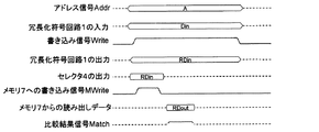
メモリ7はランダムアクセス可能な不揮発性メモリであり、書き込み又は読み出しを行うメモリの番地を指定する複数ビットのアドレス信号Addrと、書き込みのタイミングを指示する書き込み信号MWriteが与えられる。セレクタ4から出力されたデータMDinが、アドレス信号Addrで指定された番地に書き込み信号MWriteに基づくタイミングで書き込まれる。
The
比較器5は、メモリ7から読み出されたn+1ビットのデータRDoutと、冗長化符号回路1の出力RDinとを比較し、比較結果を示す比較結果信号Matchを書き込み制御回路6へ出力する。書き込み制御回路6は比較結果信号Matchの値に基づいて、選択信号Selを出力する。また、書き込み制御回路6は書き込み信号MWriteを出力する。
The
冗長化復号回路2はメモリ7から読み出されたn+1ビットのデータRDoutが与えられ、冗長化復号処理を行い、nビットのデータDoutに変換して出力する。
The
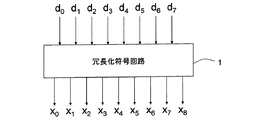
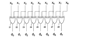
n=8を例として、冗長化符号処理及び冗長化復号処理について説明する。図2に示すように、冗長化符号回路1は8ビットのデータd0、d1、d2、d3、d4、d5、d6、d7が与えられ、冗長化符号処理を行い、9ビットのデータx0、x1、x2、x3、x4、x5、x6、x7、x8を出力する。
The redundancy coding process and the redundancy decoding process will be described by taking n = 8 as an example. As shown in FIG. 2, the
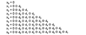
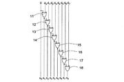
冗長化符号処理は図3に示すような論理式で表すことができ、冗長化符号回路1は図4に示すようなXOR素子11〜18を有する論理回路で構成することができる。出力するデータのビットx0として0が出力される。XOR素子11には0とビットd0が与えられ、その出力がビットx1となる。
The redundant code processing can be expressed by a logical expression as shown in FIG. 3, and the
XOR素子12にはXOR素子11の出力とビットd1とが与えられ、その出力がビットx2となる。以下同様に、XOR素子k(13≦k≦18)にはXOR素子k−1の出力とビットdk−11とが与えられ、その出力がビットxk−10となる。
The
図5に示すように、冗長化復号回路2はメモリ7から読み出された9ビットのデータx0、x1、x2、x3、x4、x5、x6、x7、x8が与えられ、冗長化復号処理を行い、8ビットのデータd0、d1、d2、d3、d4、d5、d6、d7を出力する。
As shown in FIG. 5, the
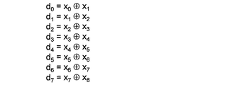
冗長化復号処理は図6に示すような論理式で表すことができ、冗長化符号回路2は図7に示すようなXOR素子21〜28を有する論理回路で構成することができる。XOR素子21にはビットx0とx1とが与えられ、その出力がビットd0となる。
The redundant decoding process can be expressed by a logical expression as shown in FIG. 6, and the
以下同様に、XOR素子j(22≦j≦28)にはビットxj−21とxj−20とが与えられ、その出力がビットdj−21となる。 Similarly, the bits x j-21 and x j-20 are given to the XOR element j (22 ≦ j ≦ 28), and the output thereof is the bit d j-21 .
図3、図6に示す論理式から分かるように、8ビットのデータd0、d1、d2、d3、d4、d5、d6、d7に対して冗長化符号処理を行って得られる9ビットのデータx0、x1、x2、x3、x4、x5、x6、x7、x8を冗長化復号処理すると、元の8ビットのデータd0、d1、d2、d3、d4、d5、d6、d7に戻すことが出来る。 As can be seen from the logical expressions shown in FIG. 3 and FIG. 6, redundant code processing is performed on 8-bit data d 0 , d 1 , d 2 , d 3 , d 4 , d 5 , d 6 , and d 7 . When the 9-bit data x 0 , x 1 , x 2 , x 3 , x 4 , x 5 , x 6 , x 7 , x 8 obtained by the redundancy decoding process are obtained, the original 8-bit data d 0 , d 1 , d 2 , d 3 , d 4 , d 5 , d 6 , d 7 can be restored.
また、9ビットのデータx0、x1、x2、x3、x4、x5、x6、x7、x8の各ビットの否定をとって(各ビットを反転して)から冗長化復号処理しても、元の8ビットのデータd0、d1、d2、d3、d4、d5、d6、d7に戻すことが出来る。 Also, 9 bits of data x 0 , x 1 , x 2 , x 3 , x 4 , x 5 , x 6 , x 7 , x 8 are negated (inverted each bit) and then redundant Even if the decoding process is performed, the original 8-bit data d 0 , d 1 , d 2 , d 3 , d 4 , d 5 , d 6 , d 7 can be restored.
例えば8ビットのデータが01100011であったとする。この値を図4に示す冗長化符号回路に与えると、9ビットのデータ001000010が出力される。この001000010を図7に示す冗長化復号回路に与えると、その出力は01100011となり、元のデータに戻る。 For example, assume that 8-bit data is 01000011. When this value is given to the redundant encoding circuit shown in FIG. 4, 9-bit data 0010000010 is output. When this 001000010 is given to the redundant decoding circuit shown in FIG. 7, the output becomes 010000011, and the original data is restored.
また、9ビットのデータ001000010の各ビットの否定をとった110111101を図7に示す冗長化復号回路に与えても、その出力は01100011となり、元のデータに戻る。 Further, even if 110111101 obtained by negating each bit of the 9-bit data 0010000010 is given to the redundant decoding circuit shown in FIG. 7, the output becomes 010000011, and the original data is restored.
冗長化符号処理後の9ビットのデータx0、x1、x2、x3、x4、x5、x6、x7、x8を記憶するメモリセルのうち、いずれか1つが常に0(又は1)しか読み出せない不良メモリセルであったとしても、その不良メモリセルに記憶させるビットの値が0(又は1)の場合はx0、x1、x2、x3、x4、x5、x6、x7、x8を書き込み、不良メモリセルに記憶させるビットの値が1(又は0)の場合はx0、x1、x2、x3、x4、x5、x6、x7、x8の各ビットの否定をとったものを書き込むようにすることで、不良メモリセルに記憶させる値と不良メモリセルから読み出せる値とを一致させることができる。 Any one of the memory cells storing 9-bit data x 0 , x 1 , x 2 , x 3 , x 4 , x 5 , x 6 , x 7 , x 8 after the redundancy code processing is always 0. Even if it is a defective memory cell that can only be read (or 1), if the value of the bit stored in the defective memory cell is 0 (or 1), x 0 , x 1 , x 2 , x 3 , x 4 , X 5 , x 6 , x 7 , x 8 are written, and when the value of the bit stored in the defective memory cell is 1 (or 0), x 0 , x 1 , x 2 , x 3 , x 4 , x 5 , X 6 , x 7 , x 8 are negated so that the value stored in the defective memory cell and the value readable from the defective memory cell can be matched.
メモリから読み出されるデータがx0、x1、x2、x3、x4、x5、x6、x7、x8、又はx0、x1、x2、x3、x4、x5、x6、x7、x8の各ビットの否定をとったもののいずれであっても、冗長化復号処理により同一のデータd0、d1、d2、d3、d4、d5、d6、d7に戻すことができるため、正しいデータの読み出しが可能となる。 The data read from the memory is x 0 , x 1 , x 2 , x 3 , x 4 , x 5 , x 6 , x 7 , x 8 , or x 0 , x 1 , x 2 , x 3 , x 4 , x The same data d 0 , d 1 , d 2 , d 3 , d 4 , d 5 is obtained by the redundant decoding process regardless of which of the negated bits of 5 , x 6 , x 7 , x 8. , D 6 , d 7 can be restored, so that correct data can be read out.
例えば、冗長化符号処理後の9ビットのデータ001000010を記憶するメモリセルのうち、左から3ビット目のメモリセルが0しか読み出せない不良メモリセルであった場合、メモリ7には各ビットの否定をとった110111101を書き込んでおけば、冗長化復号処理により、正しいデータを読み出すことができる。
For example, if the memory cell storing the 9-bit data 0010000010 after the redundancy coding process is a defective memory cell from which only 0 can be read, the
本発明の実施形態によるメモリシステムは、マイクロプロセッサ等のハードウェアに接続して、データの書き込みや読み出しを行う。このようなメモリシステムを用いたデータ書き込み方法を図8に示すフローチャートを用いて説明する。 The memory system according to the embodiment of the present invention is connected to hardware such as a microprocessor to write and read data. A data writing method using such a memory system will be described with reference to the flowchart shown in FIG.
ここでは、マイクロプロセッサがメモリシステムにデータを書き込む場合を例に説明するが、マイクロプロセッサ以外のハードウェアがデータを書き込む場合も同様である。マイクロプロセッサはメモリシステムにデータを書き込むために、書き込みたいアドレスをメモリシステムのアドレス信号Addrに出力し、書き込みたいデータをメモリシステムのデータ信号Dinに出力する。そして、マイクロプロセッサはメモリシステムの書き込み信号Writeに対する出力を論理値0から1に変化させることで、メモリシステムの書き込み処理を開始させる。
Here, a case where the microprocessor writes data to the memory system will be described as an example, but the same applies to a case where hardware other than the microprocessor writes data. In order to write data to the memory system, the microprocessor outputs an address to be written to the address signal Addr of the memory system and outputs data to be written to the data signal Din of the memory system. Then, the microprocessor changes the output for the write signal Write of the memory system from the
(ステップS100)マイクロプロセッサから、アドレス信号Addrにより、メモリ7へデータの書き込み先となるアドレスAが与えられる。また、マイクロプロセッサから、冗長化符号回路1へnビットのデータDinが与えられる。
(Step S100) From the microprocessor, an address A as a data write destination is given to the
(ステップS101)冗長化符号回路1により冗長化符号処理が行われ、n+1ビットのデータRDinが出力される。
(Step S101) Redundancy coding processing is performed by the
(ステップS102)セレクタ4がデータRDinを選択するように、書き込み制御回路6から選択信号Selが出力される。さらに、書き込み制御回路6がメモリ7への書き込み信号MWriteを論理値0から1へ変化させてメモリ7へ書き込みを指示することで、メモリ7のアドレスAにデータRDinが書き込まれる。
(Step S102) The selection signal Sel is output from the
(ステップS103)メモリ7のアドレスAからデータRDoutを読み出す。
(Step S103) Data RDout is read from address A of the
(ステップS104)比較器5においてデータRDinとデータRDoutが比較され、比較結果を示す比較結果信号Matchが出力される。書き込み制御回路6は、比較結果信号Matchが真、すなわちデータRDinとデータRDoutが一致、の場合は、データがメモリ7へ正しく書き込めていると判定し、書き込み動作を終了する。
(Step S104) The
比較結果信号Matchが偽、すなわちデータRDinとデータRDoutが不一致、の場合は、ステップS105へ進む。 If the comparison result signal Match is false, that is, if the data RDin and the data RDout do not match, the process proceeds to step S105.
(ステップS105)セレクタ4がインバータ3の出力、すなわちデータRDinの各ビットの否定をとった値“〜RDin”、を選択するように、書き込み制御回路6から選択信号Selが出力される。さらに、書き込み制御回路6がメモリ7への書き込み信号MWriteを論理値0から1に変化させてメモリ7へ書き込みを指示することで、メモリ7のアドレスAにデータ“〜RDin”が書き込まれる。
(Step S105) The selection signal Sel is output from the
ステップS104で比較結果が一致している場合のタイミングチャートは図9に示すようなものとなり、比較結果が不一致である場合のタイミングチャートは図10に示すようなものとなる。 The timing chart when the comparison results match in step S104 is as shown in FIG. 9, and the timing chart when the comparison results do not match is as shown in FIG.
ステップS104で比較結果信号Matchが真の場合に、データがメモリ7へ正しく書き込めていると判断した場合、書き込み動作を終了せずに、データRDinを再度書き込むように実施することも可能である。
If it is determined in step S104 that the comparison result signal Match is true and the data is correctly written to the
また、比較器5はメモリ7から読み出されたデータRDoutと冗長化復号回路1の出力RDinとを比較するのではなく、メモリ7から読み出されたデータRDoutとインバータ3の出力〜RDinとを比較するようにしてもよい。この場合、ステップS102ではインバータ3の出力からRDinがメモリ7に書き込まれる。そしてステップS104でデータ〜RDinとデータRDoutが比較され、不一致の場合はステップS105でデータRDinがメモリ7に書き込まれる。
The
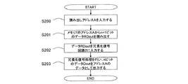
次に、データ読み出し方法を図11に示すフローチャートを用いて説明する。マイクロプロセッサはメモリシステムからデータを読み出すために、読み出したいアドレスをメモリシステムのアドレス信号Addrに出力することで、メモリシステムの読み出し処理を開始させる。 Next, a data reading method will be described using the flowchart shown in FIG. In order to read data from the memory system, the microprocessor outputs an address to be read to the address signal Addr of the memory system, thereby starting the reading process of the memory system.
(ステップS200)マイクロプロセッサから、アドレス信号AddrによりアドレスAが与えられる。 (Step S200) The address A is given from the microprocessor by the address signal Addr.
(ステップS201)メモリ7のアドレスAからn+1ビットのデータRDoutが読み出される。
(Step S201) The n + 1-bit data RDout is read from the address A of the
(ステップS202)データRDoutが冗長化復号回路2に与えられる。
(Step S202) Data RDout is provided to
(ステップS203)冗長化復号処理が行われ、nビットのデータDoutがメモリ7のアドレスAのデータとして出力される。
(Step S203) Redundant decoding processing is performed, and n-bit data Dout is output as data at address A in the
冗長化符号処理、冗長化復号処理を用いることで、メモリ7のn+1ビット分のメモリセル中に1ビットの不良メモリセルが存在していても、データの読み書きを正しく行うことができる。ここで、nの値は、メモリ7内に不良メモリセルが多いときは小さな値に設定し、不良メモリセルが少ない場合は大きな値に設定することができる。
By using the redundant encoding process and the redundant decoding process, data can be read and written correctly even if a 1-bit defective memory cell exists in the memory cells of n + 1 bits of the
上述のようなメモリアクセス方法により、通常のECCよりも高い効率で不良メモリセルを救済することができる。例えば、本実施形態によるメモリアクセス方法ではn=8とした場合、8ビットのデータに対して冗長化符号処理を行い9ビットとすることで、9ビット分のメモリセルのうち、1ビットの不良メモリセルを救済できる。つまり、8ビットのデータに1ビットの冗長ビットを付加することで1ビットの不良メモリセルを救済できる。 By the memory access method as described above, defective memory cells can be relieved with higher efficiency than normal ECC. For example, in the memory access method according to the present embodiment, when n = 8, redundancy coding processing is performed on 8-bit data to 9 bits, so that a 1-bit defect among 9-bit memory cells. The memory cell can be saved. That is, a 1-bit defective memory cell can be relieved by adding a 1-bit redundant bit to 8-bit data.
一方、データビットと冗長ビットの比率が上述の例と等しい、64ビットのデータに8ビットの冗長ビットを付加する1誤り訂正2誤り検出符号(SECDED:Single Error Correction Double Error Detection)を用いる場合は、72ビットのメモリセルのうち、1ビットの不良メモリセルしか救済することができない。
On the other hand, when using 1
本実施形態ではメモリへの書き込み時に、メモリ7への最大2回の書き込みと1回の読み出しが必要となるため、書き込みが1回で済む自己参照読み出しと比較して、書き込みの速度は低下する。
In the present embodiment, when writing to the memory, writing to the
しかし、本実施形態ではメモリからの読み出し時に1回の読み出しだけで済むのに対し、自己参照読み出しは2回の読み出し及び2回の書き込みが必要になるので、読み出し速度を高速化できる。 However, in the present embodiment, only one reading is required when reading from the memory, whereas the self-reference reading requires two readings and two writings, so that the reading speed can be increased.
一般に、メモリの書き込みは読み出しよりも頻度が少なく、読み出しが高速である方が、メモリへの総アクセス時間を低減し、メモリを効率良く使用することができる。 In general, memory writing is performed less frequently than reading, and reading at a higher speed can reduce the total access time to the memory and use the memory more efficiently.
このように、本実施形態によるメモリシステムにより、電気的に書き替え可能なメモリの不良メモリセルを高効率に救済し、かつメモリへのアクセス時間を低減してメモリを効率良く使用することができる。 As described above, the memory system according to the present embodiment can efficiently repair defective memory cells of an electrically rewritable memory and can efficiently use the memory by reducing the access time to the memory. .
上記実施形態では、メモリ7の読み書きのデータ幅と、冗長化符号処理して記憶する単位が同じであったが、異なっていてもよい。例えば、読み書きのデータ幅が16ビットで、冗長化処理の単位が8ビットの場合は、図12に示すように、16ビットのデータを上位8ビットと下位8ビットに分割し、2つの冗長化処理ブロック10a、10bに与える。ブロック毎に冗長化符号回路1a、1bで冗長化符号処理を行い、メモリ7に書き込む。
In the above embodiment, the read / write data width of the
そしてメモリ7に書き込んだデータと、メモリ7から読み出したデータとを比較器5a、5bで比較し、いずれのブロックにおいても一致していれば書き込み動作を終了する。いずれか一方のブロックで不一致の場合、不一致となったブロックはインバータ3の出力をセレクタ4で選択して出力し、メモリ7に書き込む。また、一致していた方のブロックは同じ値を再度メモリ7に書き込むようにする。
Then, the data written to the
このように、メモリ7の読み書きのデータ幅と、冗長化処理の単位が異なる場合は、冗長化処理ブロックを複数設けることで、上記実施形態と同様の効果を得ることができる。
As described above, when the read / write data width of the
上記実施形態における冗長化符号回路は図4に示すような構成に限定されない。例えば、図4に示す構成から冗長な論理素子であるXOR素子11を省き、図13に示すような構成にしてもよい。
The redundant encoding circuit in the above embodiment is not limited to the configuration shown in FIG. For example, the
また、冗長化符号回路では、図14に示すような論理式で表される冗長化符号処理を行ってもよい。このような処理を行う冗長化符号回路は図15(a)、(b)に示すような構成の論理回路で実現可能である。 Further, in the redundant code circuit, redundant code processing represented by a logical expression as shown in FIG. 14 may be performed. A redundant encoding circuit that performs such processing can be realized by a logic circuit having a configuration as shown in FIGS.
また、図16に示すような論理式で表される冗長化符号処理を行ってもよい。このような処理を行う冗長化符号回路は図17(a)、(b)に示すような構成の論理回路で実現可能である。また、図18に示すような論理式で表される冗長化符号処理を行ってもよい。このような処理を行う冗長化符号回路は図19(a)、(b)に示すような構成の論理回路で実現可能である。 Further, redundant code processing represented by a logical expression as shown in FIG. 16 may be performed. A redundant encoding circuit that performs such processing can be realized by a logic circuit having a configuration as shown in FIGS. Further, a redundant code process represented by a logical expression as shown in FIG. 18 may be performed. A redundant encoding circuit that performs such processing can be realized by a logic circuit having a configuration as shown in FIGS.
図17や図19に示す冗長化符号回路は、図13や図15に示す冗長化符号回路と比較して、XOR素子の段数が少ないため、高速に動作することができる。 The redundant encoding circuit shown in FIGS. 17 and 19 can operate at high speed because the number of XOR elements is smaller than that of the redundant encoding circuit shown in FIGS.
冗長化符号処理を行ったn+1ビットのデータのうち0又は1に固定する1ビットは1ビット目〜n+1ビット目のいずれでもよい。0又は1に固定するビットは、n+1ビットの中でより中央のビットである程、冗長化符号回路における論路素子の段数が少なくなり、高速動作が可能となる。 The 1 bit fixed to 0 or 1 among the n + 1 bit data subjected to the redundancy code processing may be any of the 1st bit to the (n + 1) th bit. As the bit fixed to 0 or 1 is the central bit among n + 1 bits, the number of stages of logic elements in the redundant coding circuit is reduced, and high-speed operation is possible.
上述した実施の形態は一例であって限定的なものではないと考えられるべきである。本発明の技術的範囲は特許請求の範囲によって示され、特許請求の範囲と均等の意味および範囲内でのすべての変更が含まれることが意図される。 The above-described embodiment is an example and should not be considered as limiting. The technical scope of the present invention is defined by the terms of the claims, and is intended to include any modifications within the scope and meaning equivalent to the terms of the claims.
1 冗長化符号回路
2 冗長化復号回路
3 インバータ
4 セレクタ
5 比較器
6 書き込み制御回路
7 メモリ
DESCRIPTION OF
Claims (20)
前記冗長化符号回路により冗長化符号処理されたデータが与えられ、前記冗長化符号処理されたデータの各ビットの値を反転するインバータ回路と、
前記冗長化符号処理されたデータ及び前記インバータ回路により反転されたデータが与えられ、選択信号に基づいていずれか一方を選択するセレクタと、
前記セレクタで選択されたデータを記憶するメモリと、
前記メモリから読み出されるデータと、前記冗長化符号処理されたデータ及び前記インバータ回路により反転されたデータのいずれか一方とを比較し、比較結果を示す比較結果信号を出力する比較器と、
前記メモリの書き込み制御を行うと共に、前記比較結果信号が与えられ、前記比較結果信号に示される前記比較結果に基づいて前記選択信号を生成し出力する書き込み制御回路と、
前記メモリから読み出されるデータを冗長化復号処理して出力する冗長化復号回路と、
を備えるメモリシステム。 A redundant encoding circuit for performing redundant encoding processing of write data;
Inverter circuit which is provided with data subjected to redundancy code processing by the redundancy code circuit and inverts the value of each bit of the data subjected to redundancy code processing;
A selector that receives the data subjected to the redundancy code processing and the data inverted by the inverter circuit, and selects either one based on a selection signal;
A memory for storing data selected by the selector;
A comparator that compares the data read from the memory with either the data subjected to the redundancy code processing or the data inverted by the inverter circuit, and outputs a comparison result signal indicating a comparison result;
A write control circuit that performs write control of the memory, is provided with the comparison result signal, and generates and outputs the selection signal based on the comparison result indicated in the comparison result signal;
A redundant decoding circuit that outputs the data read from the memory by performing a redundant decoding process;
A memory system comprising:
前記比較器が前記メモリから読み出されるデータと前記インバータ回路により反転されたデータとを比較する場合、前記書き込み制御回路は、前記セレクタが前記インバータ回路により反転されたデータを選択して出力するように前記選択信号を出力すると共に、前記書き込み信号を出力し、さらに、前記比較結果が不一致を示す時は前記セレクタが前記冗長化符号処理されたデータを選択して出力するように前記選択信号を出力すると共に、前記書き込み信号を出力することを特徴とする請求項1に記載のメモリシステム。 When the comparator compares the data read from the memory and the data subjected to the redundancy code processing, the write control circuit selects and outputs the data subjected to the redundancy code processing by the selector. In addition to outputting the selection signal, a write signal indicating a write timing to the memory is output, and when the comparison result indicates a mismatch, the selector selects and outputs the data inverted by the inverter circuit And outputting the selection signal and outputting the write signal,
When the comparator compares the data read from the memory with the data inverted by the inverter circuit, the write control circuit selects and outputs the data inverted by the inverter circuit Outputs the selection signal and the write signal, and further outputs the selection signal so that the selector selects and outputs the data subjected to the redundancy code processing when the comparison result indicates a mismatch. The memory system according to claim 1, wherein the write signal is output.
第1のXORゲートには前記書き込みデータの1ビット目と2ビット目とが与えられ、
第kのXORゲート(kは2≦k≦n−1を満たす整数)には第k−1のXORゲートの出力値と前記書き込みデータのk+1ビット目が与えられ、
出力の1ビット目として0を出力し、2ビット目として前記書き込みデータの1ビット目と同じ値を出力し、3ビット目として前記第1のXORゲートの出力値を出力し、k+2ビット目として前記第kのXORゲートの出力値を出力することを特徴とする請求項4に記載のメモリシステム。 The redundant coding circuit has n-1 XOR gates,
The first XOR gate is given the first bit and the second bit of the write data,
The k-th XOR gate (k is an integer satisfying 2 ≦ k ≦ n−1) is given the output value of the (k−1) -th XOR gate and the (k + 1) th bit of the write data,
0 is output as the first bit of output, the same value as the first bit of the write data is output as the second bit, the output value of the first XOR gate is output as the third bit, and the k + 2th bit is output 5. The memory system according to claim 4, wherein an output value of the kth XOR gate is output.
第1のXORゲートには前記書き込みデータの1ビット目と1とが与えられ、
第kのXORゲート(kは2≦k≦nを満たす整数)には第k−1のXORゲートの出力値と前記書き込みデータのkビット目が与えられ、
出力の1ビット目として1を出力し、2ビット目として前記第1のXORゲートの出力値を出力し、k+1ビット目として前記第kのXORゲートの出力値を出力することを特徴とする請求項4に記載のメモリシステム。 The redundant code circuit has n XOR gates,
The first XOR gate is given the first bit and 1 of the write data,
The k-th XOR gate (k is an integer satisfying 2 ≦ k ≦ n) is given the output value of the (k−1) -th XOR gate and the k-th bit of the write data,
1 is output as the first bit of the output, the output value of the first XOR gate is output as the second bit, and the output value of the kth XOR gate is output as the k + 1 bit. Item 5. The memory system according to Item 4.
前記NOTゲートには前記書き込みデータの1ビット目が与えられ、
第1のXORゲートには前記NOTゲートの出力値と前記書き込みデータの2ビット目とが与えられ、
第kのXORゲート(kは2≦k≦n−1を満たす整数)には第k−1のXORゲートの出力値と前記書き込みデータのk+1ビット目が与えられ、
出力の1ビット目として1を出力し、2ビット目として前記NOTゲートの出力値を出力し、3ビット目として前記第1のXORゲートの出力値を出力し、k+2ビット目として前記第kのXORゲートの出力値を出力することを特徴とする請求項4に記載のメモリシステム。 The redundant code circuit has a NOT gate and n-1 XOR gates,
The first gate of the write data is given to the NOT gate,
The first XOR gate is given the output value of the NOT gate and the second bit of the write data,
The k-th XOR gate (k is an integer satisfying 2 ≦ k ≦ n−1) is given the output value of the (k−1) -th XOR gate and the (k + 1) th bit of the write data,
1 is output as the first bit of output, the output value of the NOT gate is output as the second bit, the output value of the first XOR gate is output as the third bit, and the k-th bit is output as the k + 2 bit. 5. The memory system according to claim 4, wherein an output value of the XOR gate is output.
第1のXORゲートには前記書き込みデータのmビット目とm−1ビット目が与えられ、
第jのXORゲート(jは2≦j≦m−1を満たす整数)には第j−1のXORゲートの出力値と前記書き込みデータのm−jビット目が与えられ、
第mのXORゲートには前記書き込みデータのm+1ビット目とm+2ビット目が与えられ、
第kのXORゲート(kはm+1≦k≦2m−2を満たす整数)には第k−1のXORゲートの出力値と前記書き込みデータのk+2ビット目が与えられ、
出力のm−jビット目として前記第jのXORゲートの出力値を出力し、m−1ビット目として前記第1のXORゲートの出力値を出力し、mビット目として前記書き込みデータのmビット目と同じ値を出力し、m+1ビット目として0を出力し、m+2ビット目として前記書き込みデータのm+1ビット目と同じ値を出力し、m+3ビット目として前記第mのXORゲートの出力値を出力し、k+3ビット目の出力として前記第kのXORゲートの出力値を出力することを特徴とする請求項4に記載のメモリシステム。 The redundant coding circuit has 2m−2 (m is an integer satisfying 2m = n) XOR gates,
The first XOR gate is provided with the mth bit and the m−1th bit of the write data,
The jth XOR gate (j is an integer satisfying 2 ≦ j ≦ m−1) is given the output value of the j−1 XOR gate and the m−jth bit of the write data,
The (m + 1) th bit and the (m + 2) th bit of the write data are given to the mth XOR gate,
The k-th XOR gate (k is an integer satisfying m + 1 ≦ k ≦ 2m−2) is given the output value of the (k−1) -th XOR gate and the k + 2th bit of the write data,
The output value of the jth XOR gate is output as the m-jth bit of the output, the output value of the first XOR gate is output as the m-1th bit, and the m bits of the write data as the mth bit Outputs the same value as the first, outputs 0 as the m + 1 bit, outputs the same value as the m + 1 bit of the write data as the m + 2 bit, and outputs the output value of the mth XOR gate as the m + 3 bit 5. The memory system according to claim 4, wherein an output value of the kth XOR gate is output as an output of the (k + 3) th bit.
第1のXORゲートには前記書き込みデータのmビット目と1とが与えられ、
第jのXORゲート(jは2≦j≦mを満たす整数)には第j−1のXORゲートの出力値と前記書き込みデータのm−j+1ビット目が与えられ、
第m+1のXORゲートには前記書き込みデータのm+1ビット目と1とが与えられ、
第kのXORゲート(kはm+2≦k≦2mを満たす整数)には第k−1のXORゲートの出力値と前記書き込みデータのkビット目が与えられ、
出力のm−j+1ビット目として前記第jのXORゲートの出力値を出力し、mビット目として前記第1のXORゲートの出力値を出力し、m+1ビット目として1を出力し、m+2ビット目として前記第m+1のXORゲートの出力値を出力し、k+1ビット目の出力として前記第kのXORゲートの出力値を出力することを特徴とする請求項4に記載のメモリシステム。 The redundant code circuit has 2m (m is an integer satisfying 2m = n) XOR gates,
The first XOR gate is given the m-th bit and 1 of the write data,
The jth XOR gate (j is an integer satisfying 2 ≦ j ≦ m) is given the output value of the (j−1) th XOR gate and the m−j + 1 bit of the write data,
The (m + 1) th XOR gate is given the (m + 1) th bit of the write data and 1;
The k-th XOR gate (k is an integer satisfying m + 2 ≦ k ≦ 2m) is given the output value of the (k−1) -th XOR gate and the k-th bit of the write data,
The output value of the jth XOR gate is output as the (m−j + 1) th bit of the output, the output value of the first XOR gate is output as the mth bit, 1 is output as the m + 1th bit, and the m + 2th bit 5. The memory system according to claim 4, wherein an output value of the (m + 1) th XOR gate is output as an output value, and an output value of the kth XOR gate is output as an output of the (k + 1) th bit.
第1のNOTゲートには前記書き込みデータのmビット目が与えられ、
第2のNOTゲートには前記書き込みデータのm+1ビット目が与えられ、
第1のXORゲートには前記書き込みデータのm−1ビット目と前記第1のNOTゲートの出力値とが与えられ、
第jのXORゲート(jは2≦j≦m−1を満たす整数)には第j−1のXORゲートの出力値と前記書き込みデータのm−jビット目が与えられ、
第mのXORゲートには前記書き込みデータのm+2ビット目と前記第2のNOTゲートの出力値とが与えられ、
第kのXORゲート(kはm+1≦k≦2m−2を満たす整数)には第k−1のXORゲートの出力値と前記書き込みデータのk+2ビット目が与えられ、
出力のm−jビット目として前記第jのXORゲートの出力値を出力し、m−1ビット目とし前記第1のXORゲートの出力値を出力し、mビット目として前記第1のNOTゲートの出力値を出力し、m+1ビット目として1を出力し、m+2ビット目として前記第2のNOTゲートの出力値を出力し、m+3ビット目として前記第mのXORゲートの出力値を出力し、k+3ビット目の出力として前記第kのXORゲートの出力値を出力することを特徴とする請求項4に記載のメモリシステム。 The redundancy code circuit has 2m-2 (m is an integer satisfying 2m = n) XOR gates and two NOT gates,
The m-th bit of the write data is given to the first NOT gate,
The second NOT gate is given the (m + 1) th bit of the write data,
The first XOR gate is given the (m−1) th bit of the write data and the output value of the first NOT gate,
The jth XOR gate (j is an integer satisfying 2 ≦ j ≦ m−1) is given the output value of the j−1 XOR gate and the m−jth bit of the write data,
The m + 2th bit of the write data and the output value of the second NOT gate are given to the mth XOR gate,
The k-th XOR gate (k is an integer satisfying m + 1 ≦ k ≦ 2m−2) is given the output value of the (k−1) -th XOR gate and the k + 2th bit of the write data,
The output value of the jth XOR gate is output as the m-jth bit of the output, the output value of the first XOR gate is output as the m-1th bit, and the first NOT gate is output as the mth bit. , 1 is output as the m + 1 bit, the output value of the second NOT gate is output as the m + 2 bit, and the output value of the m th XOR gate is output as the m + 3 bit, 5. The memory system according to claim 4, wherein an output value of the kth XOR gate is output as an output of the (k + 3) th bit.
第kのXORゲート(kは1≦k≦nを満たす整数)には前記メモリから読み出されるデータのkビット目とk+1ビット目が与えられ、
出力のkビット目として前記第kのXORゲートの出力値を出力することを特徴とする請求項4に記載のメモリシステム。 The redundant decoding circuit has n XOR gates,
The k-th XOR gate (k is an integer satisfying 1 ≦ k ≦ n) is given the k-th and k + 1-th bits of the data read from the memory,
5. The memory system according to claim 4, wherein an output value of the k-th XOR gate is output as a k-th output bit.
前記冗長化符号処理した書き込みデータ及び前記冗長化符号処理した書き込みデータの各ビットの値を反転したデータのいずれか一方をメモリの、アドレス信号により指定されたアドレスに書き込み、
前記メモリの前記指定されたアドレスからデータを読み出し、
前記メモリへ書き込んだデータと、前記メモリから読み出したデータとを比較し、
比較結果が不一致であれば前記冗長化符号処理した書き込みデータ及び前記冗長化符号処理した書き込みデータの各ビットの値を反転したデータの他方を前記メモリの前記指定されたアドレスに書き込むメモリアクセス方法。 Redundant code processing of write data,
Write either one of the write data subjected to the redundancy code processing and the data obtained by inverting the value of each bit of the write data subjected to the redundancy code processing to an address specified by an address signal in the memory,
Reading data from the specified address of the memory;
Compare the data written to the memory with the data read from the memory,
A memory access method for writing the other of the write data subjected to the redundancy code processing and the data obtained by inverting the value of each bit of the write data subjected to the redundancy code processing to the designated address of the memory if the comparison result is inconsistent.
出力の1ビット目として0を出力し、
出力の2ビット目として前記書き込みデータの1ビット目と同じ値を出力し、
出力のkビット目(kは2≦k≦nを満たす整数)の値と前記書き込みデータのkビット目の値とのXORを演算し、演算結果を出力のk+1ビット目として出力することを特徴とする請求項15に記載のメモリアクセス方法。 The redundant code processing is:
Output 0 as the first bit of output,
Output the same value as the first bit of the write data as the second bit of output,
XOR of the value of the k-th output (k is an integer satisfying 2 ≦ k ≦ n) and the value of the k-th bit of the write data is calculated, and the calculation result is output as the (k + 1) -th output bit. The memory access method according to claim 15.
出力の1ビット目として1を出力し、
出力に2ビット目として前記書き込みデータの1ビット目の否定をとった値を出力し、
出力のkビット目(kは2≦k≦nを満たす整数)の値と前記書き込みデータのkビット目の値とのXORを演算し、演算結果を出力のk+1ビット目として出力することを特徴とする請求項15に記載のメモリアクセス方法。 The redundant code processing is:
1 is output as the first bit of output,
Output the negative value of the first bit of the write data as the second bit in the output,
XOR of the value of the k-th output (k is an integer satisfying 2 ≦ k ≦ n) and the value of the k-th bit of the write data is calculated, and the calculation result is output as the (k + 1) -th output bit. The memory access method according to claim 15.
出力のm+1ビット目(mは2m=nを満たす整数)として0を出力し、
出力のmビット目として前記書き込みデータのmビット目と同じ値を出力し、
出力のjビット目(jは2≦j≦mを満たす整数)と前記書き込みデータのj−1ビット目とのXORを演算し、演算結果を出力のj−1ビット目として出力し、
出力のm+2ビット目として前記書き込みデータのm+1ビット目と同じ値を出力し、
出力のkビット目(kはm+2≦k≦2mを満たす整数)と前記書き込みデータのkビット目とのXORを演算し、演算結果を出力のk+1ビット目として出力することを特徴とする請求項15に記載のメモリアクセス方法。 The redundant code processing is:
Output 0 as the (m + 1) th bit of output (m is an integer satisfying 2m = n),
Output the same value as the mth bit of the write data as the mth bit of output,
XOR of the output j-th bit (j is an integer satisfying 2 ≦ j ≦ m) and the j−1-th bit of the write data is calculated, and the calculation result is output as the j−1-th output bit,
Output the same value as the (m + 1) th bit of the write data as the (m + 2) th bit of the output,
The XOR of the k-th output (k is an integer satisfying m + 2 ≦ k ≦ 2m) and the k-th bit of the write data is calculated, and the calculation result is output as the (k + 1) -th output. 15. The memory access method according to 15.
出力のm+1ビット目(mは2m=nを満たす整数)として1を出力し、
出力のmビット目として前記書き込みデータのmビット目の否定をとった値を出力し、
出力のjビット目(jは2≦j≦mを満たす整数)と前記書き込みデータのj−1ビット目とのXORを演算し、演算結果を出力のj−1ビット目として出力し、
出力のm+2ビット目として前記書き込みデータのm+1ビット目の否定をとった値を出力し、
出力のkビット目(kはm+2≦k≦2mを満たす整数)と前記書き込みデータのkビット目とのXORを演算し、演算結果を出力のk+1ビット目として出力することを特徴とする請求項15に記載のメモリアクセス方法。 The redundant code processing is:
1 is output as the (m + 1) th bit of output (m is an integer satisfying 2m = n),
Output the negative value of the m-th write data as the m-th output bit,
XOR of the output j-th bit (j is an integer satisfying 2 ≦ j ≦ m) and the j−1-th bit of the write data is calculated, and the calculation result is output as the j−1-th output bit,
Output the negated value of the m + 1 bit of the write data as the m + 2 bit of the output,
The XOR of the k-th output (k is an integer satisfying m + 2 ≦ k ≦ 2m) and the k-th bit of the write data is calculated, and the calculation result is output as the (k + 1) -th output. 15. The memory access method according to 15.
Priority Applications (2)
| Application Number | Priority Date | Filing Date | Title |
|---|---|---|---|
| JP2008164205A JP5283989B2 (en) | 2008-06-24 | 2008-06-24 | Memory system and memory access method |
| US12/393,251 US8166356B2 (en) | 2008-06-24 | 2009-02-26 | Memory system and memory access method |
Applications Claiming Priority (1)
| Application Number | Priority Date | Filing Date | Title |
|---|---|---|---|
| JP2008164205A JP5283989B2 (en) | 2008-06-24 | 2008-06-24 | Memory system and memory access method |
Related Child Applications (1)
| Application Number | Title | Priority Date | Filing Date |
|---|---|---|---|
| JP2013111086A Division JP5492329B2 (en) | 2013-05-27 | 2013-05-27 | Memory access device |
Publications (2)
| Publication Number | Publication Date |
|---|---|
| JP2010009101A true JP2010009101A (en) | 2010-01-14 |
| JP5283989B2 JP5283989B2 (en) | 2013-09-04 |
Family
ID=41432522
Family Applications (1)
| Application Number | Title | Priority Date | Filing Date |
|---|---|---|---|
| JP2008164205A Expired - Fee Related JP5283989B2 (en) | 2008-06-24 | 2008-06-24 | Memory system and memory access method |
Country Status (2)
| Country | Link |
|---|---|
| US (1) | US8166356B2 (en) |
| JP (1) | JP5283989B2 (en) |
Cited By (1)
| Publication number | Priority date | Publication date | Assignee | Title |
|---|---|---|---|---|
| JP2012235272A (en) * | 2011-04-28 | 2012-11-29 | Fujitsu Ltd | Semiconductor device, information processing apparatus and error detection method |
Families Citing this family (4)
| Publication number | Priority date | Publication date | Assignee | Title |
|---|---|---|---|---|
| JP5283989B2 (en) * | 2008-06-24 | 2013-09-04 | 株式会社東芝 | Memory system and memory access method |
| JP5284069B2 (en) | 2008-12-11 | 2013-09-11 | 株式会社東芝 | Memory system and memory access method |
| JP5010756B2 (en) | 2009-09-09 | 2012-08-29 | 株式会社東芝 | Memory device |
| CN114138203B (en) * | 2021-12-06 | 2024-02-06 | 武汉新芯集成电路制造有限公司 | Data access method, data storage method and data access controller |
Citations (5)
| Publication number | Priority date | Publication date | Assignee | Title |
|---|---|---|---|---|
| JPS5580893A (en) * | 1978-12-01 | 1980-06-18 | Fujitsu Ltd | Memory device |
| JPH01108655A (en) * | 1987-10-22 | 1989-04-25 | Hitachi Ltd | System for detecting error or readout data in memory system |
| JPH01295349A (en) * | 1988-05-23 | 1989-11-29 | Seiko Instr Inc | Semiconductor nonvolatile memory device |
| JPH06214891A (en) * | 1991-10-18 | 1994-08-05 | Texas Instr Inc <Ti> | Circuit and method for masking of data |
| JP2004031904A (en) * | 2002-04-10 | 2004-01-29 | Hewlett Packard Co <Hp> | Memory cell |
Family Cites Families (12)
| Publication number | Priority date | Publication date | Assignee | Title |
|---|---|---|---|---|
| JPH071493B2 (en) * | 1987-06-11 | 1995-01-11 | 三菱電機株式会社 | Test auxiliary circuit |
| KR0169267B1 (en) * | 1993-09-21 | 1999-02-01 | 사토 후미오 | Nonvolatile semiconductor memory device |
| JP2001351398A (en) * | 2000-06-12 | 2001-12-21 | Nec Corp | Storage device |
| JP3537087B2 (en) * | 2000-09-29 | 2004-06-14 | Necエレクトロニクス株式会社 | Semiconductor device and method of inspecting semiconductor device |
| JP4400081B2 (en) * | 2003-04-08 | 2010-01-20 | エルピーダメモリ株式会社 | Semiconductor memory device |
| DE10337854A1 (en) * | 2003-08-18 | 2005-03-31 | Infineon Technologies Ag | Integrated memory with a test circuit for the function test of the memory |
| US7106621B2 (en) * | 2004-06-30 | 2006-09-12 | Stmicroelectronics, Inc. | Random access memory array with parity bit structure |
| US7565586B2 (en) * | 2006-05-25 | 2009-07-21 | Honeywell International Inc. | Method and apparatus for latent fault memory scrub in memory intensive computer hardware |
| JP2008159089A (en) * | 2006-12-20 | 2008-07-10 | Toshiba Corp | Self test circuit device and its self test method |
| US7747913B2 (en) * | 2007-08-03 | 2010-06-29 | Intel Corporation | Correcting intermittent errors in data storage structures |
| US20090091968A1 (en) * | 2007-10-08 | 2009-04-09 | Stefan Dietrich | Integrated circuit including a memory having a data inversion circuit |
| JP5283989B2 (en) * | 2008-06-24 | 2013-09-04 | 株式会社東芝 | Memory system and memory access method |
-
2008
- 2008-06-24 JP JP2008164205A patent/JP5283989B2/en not_active Expired - Fee Related
-
2009
- 2009-02-26 US US12/393,251 patent/US8166356B2/en active Active
Patent Citations (5)
| Publication number | Priority date | Publication date | Assignee | Title |
|---|---|---|---|---|
| JPS5580893A (en) * | 1978-12-01 | 1980-06-18 | Fujitsu Ltd | Memory device |
| JPH01108655A (en) * | 1987-10-22 | 1989-04-25 | Hitachi Ltd | System for detecting error or readout data in memory system |
| JPH01295349A (en) * | 1988-05-23 | 1989-11-29 | Seiko Instr Inc | Semiconductor nonvolatile memory device |
| JPH06214891A (en) * | 1991-10-18 | 1994-08-05 | Texas Instr Inc <Ti> | Circuit and method for masking of data |
| JP2004031904A (en) * | 2002-04-10 | 2004-01-29 | Hewlett Packard Co <Hp> | Memory cell |
Cited By (1)
| Publication number | Priority date | Publication date | Assignee | Title |
|---|---|---|---|---|
| JP2012235272A (en) * | 2011-04-28 | 2012-11-29 | Fujitsu Ltd | Semiconductor device, information processing apparatus and error detection method |
Also Published As
| Publication number | Publication date |
|---|---|
| JP5283989B2 (en) | 2013-09-04 |
| US20090319867A1 (en) | 2009-12-24 |
| US8166356B2 (en) | 2012-04-24 |
Similar Documents
| Publication | Publication Date | Title |
|---|---|---|
| US8069389B2 (en) | Error correction circuit and method, and semiconductor memory device including the circuit | |
| TWI697000B (en) | Memory controller and method of accessing flash memory | |
| US20220004457A1 (en) | Nonvolatile memory device and memory system including nonvolatile memory device | |
| JP6602904B2 (en) | Processing data in memory cells of memory | |
| US9547551B2 (en) | Memory system having an encoding processing circuit for redundant encoding process | |
| KR20080106849A (en) | Reproduction device | |
| JP2010218634A (en) | Error detector/corrector, memory controller, and semiconductor memory device | |
| US10741212B2 (en) | Error correction code (ECC) encoders, ECC encoding methods capable of encoding for one clock cycle, and memory controllers including the ECC encoders | |
| JP5283989B2 (en) | Memory system and memory access method | |
| US20110058415A1 (en) | Systems and Methods for Increasing Bit Density in a Memory Cell | |
| JP5520390B2 (en) | Apparatus and method for processing data element sequence | |
| US10191801B2 (en) | Error correction code management of write-once memory codes | |
| US20080082870A1 (en) | Parallel bit test device and method using error correcting code | |
| US8351257B2 (en) | Semiconductor memory device and method of reading the same | |
| TW201320090A (en) | Data modification based on matching bit patterns | |
| JP2017022651A (en) | Error correction device, semiconductor storing device, and error correction method | |
| JP6018508B2 (en) | Nonvolatile semiconductor memory device and test method thereof | |
| JP2017107620A (en) | Semiconductor device and nonvolatile memory | |
| CN110716824A (en) | Encoding method and memory storage device using the same | |
| JP5492329B2 (en) | Memory access device | |
| JP4099844B2 (en) | Memory device | |
| US9239751B1 (en) | Compressing data from multiple reads for error control management in memory systems | |
| JPH11212876A (en) | Coding method and memory using the same | |
| JP5563125B2 (en) | Memory access device | |
| KR20090048142A (en) | Ecc processing unit of non volatile memory device |
Legal Events
| Date | Code | Title | Description |
|---|---|---|---|
| A621 | Written request for application examination |
Free format text: JAPANESE INTERMEDIATE CODE: A621 Effective date: 20110324 |
|
| A131 | Notification of reasons for refusal |
Free format text: JAPANESE INTERMEDIATE CODE: A131 Effective date: 20130205 |
|
| A521 | Request for written amendment filed |
Free format text: JAPANESE INTERMEDIATE CODE: A523 Effective date: 20130401 |
|
| TRDD | Decision of grant or rejection written | ||
| A01 | Written decision to grant a patent or to grant a registration (utility model) |
Free format text: JAPANESE INTERMEDIATE CODE: A01 Effective date: 20130507 |
|
| A61 | First payment of annual fees (during grant procedure) |
Free format text: JAPANESE INTERMEDIATE CODE: A61 Effective date: 20130529 |
|
| R151 | Written notification of patent or utility model registration |
Ref document number: 5283989 Country of ref document: JP Free format text: JAPANESE INTERMEDIATE CODE: R151 |
|
| S111 | Request for change of ownership or part of ownership |
Free format text: JAPANESE INTERMEDIATE CODE: R313111 |
|
| R350 | Written notification of registration of transfer |
Free format text: JAPANESE INTERMEDIATE CODE: R350 |
|
| S111 | Request for change of ownership or part of ownership |
Free format text: JAPANESE INTERMEDIATE CODE: R313111 |
|
| R350 | Written notification of registration of transfer |
Free format text: JAPANESE INTERMEDIATE CODE: R350 |
|
| LAPS | Cancellation because of no payment of annual fees |