JP2010008698A - Electronic paper - Google Patents
Electronic paper Download PDFInfo
- Publication number
- JP2010008698A JP2010008698A JP2008167700A JP2008167700A JP2010008698A JP 2010008698 A JP2010008698 A JP 2010008698A JP 2008167700 A JP2008167700 A JP 2008167700A JP 2008167700 A JP2008167700 A JP 2008167700A JP 2010008698 A JP2010008698 A JP 2010008698A
- Authority
- JP
- Japan
- Prior art keywords
- electronic paper
- work area
- area
- display
- electrode
- Prior art date
- Legal status (The legal status is an assumption and is not a legal conclusion. Google has not performed a legal analysis and makes no representation as to the accuracy of the status listed.)
- Granted
Links
Images


Abstract
Description
本発明は、パンチ穴あけや、ホッチキス止めをすることができる電子ペーパーに関する。 The present invention relates to an electronic paper that can be punched and stapled.
近年、電子ペーパーの薄型化、フレキシブル化に向けた研究開発が進み、薄くて曲げられる電子ペーパーも登場してきている。そのような電子ペーパーは、書き換え可能な紙として、従来の紙と同様に複数枚が一緒に使用され、それらをまとめるためにパンチ穴を空けてバインダに綴じたり、ホッチキス止めにより綴じたりしたいという要望があった。そこで、電子ペーパーの機能に支障を生じさせることなく、パンチ穴をあけたり、ホッチキス止めをしたりすることのできる電子ペーパーが従来から提案されている(例えば、特許文献1参照)。特許文献1の電子ペーパーは、表示部等の機能部がない隅部や側部に穴あけ領域を設けた構成となっている。
上記特許文献1の電子ペーパーは、穴あけやホッチキス止めのための領域を、電子ペーパーの表示領域ではなく、周辺の外枠部分に設けるものであった。そのため、外枠の分だけ表示に使用できる領域が減るか、もしくは、外枠の分だけ用紙としての大きさが大きくなってしまうといった問題があった。 In the electronic paper disclosed in Patent Document 1, a region for punching and staples is provided not in the display region of the electronic paper but in a peripheral outer frame portion. For this reason, there is a problem that the area that can be used for display is reduced by the amount of the outer frame, or the size of the paper is increased by the amount of the outer frame.
紙本来の使用目的を考えると、現状の紙と同じ定型サイズであることが望ましく、出来るだけ紙の広い範囲を表示に使えるべきであり、表示領域内に穴あけやホッチキス止めができることが望ましい。 Considering the original purpose of use of paper, it is desirable that the paper has the same fixed size as that of the current paper, and a wide range of paper should be used for display as much as possible.
電子ペーパーの表示領域には、表示のための電子インク材料(液体、粉末など方式によって様々な材料が存在する)が封じ込められており、また表示内容を制御するための回路や配線が存在するため、表示領域に対して単純に穴あけやホッチキス止めを行うと、封じ込められた電子インク材料の漏れ出しや、配線が切断されることによる動作不良など、さまざまな不具合が発生する可能性がある。 The electronic paper display area contains electronic ink materials for display (various materials such as liquids and powders are contained), and there are circuits and wiring for controlling the display contents. If the display area is simply punched or stapled, various problems such as leakage of the encapsulated electronic ink material and malfunction due to disconnection of the wiring may occur.
本発明はかかる問題点を解決すべく創案されたもので、その目的は、インク漏れや動作不良を生じさせることなく、表示領域内に穴あけやホッチキス止めを行うことを可能とした電子ペーパーを提供することにある。 The present invention was devised to solve such problems, and an object thereof is to provide an electronic paper that can perform punching and stapling in a display area without causing ink leakage or malfunction. There is to do.
上記課題を解決するため、本発明の電子ペーパーは、表示領域内に穴あけ用またはホッチキス止め用の作業領域を設け、制御用の回路及び配線は前記作業領域を回避させて配置することにより、表示領域を広くとっても、穴あけやホッチキス止めにより、動作不良を生じることのない電子ペーパーを実現することができる。 In order to solve the above-described problems, the electronic paper of the present invention provides a work area for punching or stapling in the display area, and the control circuit and wiring are arranged so as to avoid the work area. Even if the area is wide, electronic paper that does not cause malfunction can be realized by drilling or staple.
また、前記作業領域内は表示用の電子インク材料を封止(充填)しないことにより、穴あけやホッチキス止めを行っても、インク漏れを生じることのない電子ペーパーを実現することができる。 Further, by not sealing (filling) the display electronic ink material in the working area, it is possible to realize an electronic paper that does not cause ink leakage even when perforated or stapled.
ここで、前記ホッチキス止め用の作業領域は、矩形形状の前記表示領域の各角隅部の4箇所またはそれらのうちの一部に設けられていることが好ましい。表示領域の対角線上の角隅部の2箇所または各角隅部の4箇所に設けることで、表示領域への表示が上下逆になっても、その表示方向に合わせた角隅部の1箇所にホッチキス止めを行うことが可能となる。あるいは、表示領域の一辺の両端の角隅部の2箇所または各角隅部の4箇所に設けることで、電子ペーパーを縦長で使用する場合及び横長で使用する場合のどちらでも、電子ペーパーの向きに応じた角隅部の1箇所にホッチキス止めを行うことが可能となる。これらにより、使用者は、電子ペーパーを使用するに際して、その向きを気にすることなく使用することができる。 Here, it is preferable that the work area for the stapler is provided at four corners of the rectangular display area or a part of them. Even if the display in the display area is upside down by providing it at two corner corners on the diagonal of the display area or at four corner corners, one corner corner that matches the display direction The stapler can be stapled. Alternatively, the orientation of the electronic paper can be used both vertically and horizontally by providing it at two corners or four corners on each side of the display area. The stapler can be stapled at one corner. Thus, the user can use the electronic paper without worrying about its orientation.
また、前記穴あけ用の作業領域は、矩形形状の前記表示領域の上下左右の各辺近傍または前記各辺の一部の近傍に設けられていることが好ましい。表示領域の左右に対向する各辺近傍及び/または上下に対向する各辺近傍に設けることで、表示領域への表示が上下逆になっても、その表示方向に合わせた辺側にファイリング用の穴をあけることができる。ただし、このような穴あけ用の作業領域をホッチキス止めすることも可能であり、ホッチキス止め用の作業領域に穴をあけることも可能である。これにより、使用者は、電子ペーパーを使用するに際して、その向きを気にすることなく使用することができる。 In addition, it is preferable that the drilling work area is provided in the vicinity of each of the upper, lower, left and right sides of the rectangular display area or in the vicinity of a part of each of the sides. By providing it near each side facing the left and right sides of the display area and / or near each side facing the top and bottom, even if the display in the display area is upside down, the side for matching the display direction can be used for filing. A hole can be drilled. However, it is possible to staple the work area for drilling, and it is also possible to make a hole in the work area for staple. Thereby, the user can use the electronic paper without worrying about the direction of the electronic paper.
また、前記穴あけ用の作業領域に、製造過程で穴あけを行っておいても良い。これにより、穴あけ作業時に作業領域外に穴をあけてしまう失敗を避けることが可能で、かつ、正確な位置に穴あけを行えるため、作業領域を必要最小限の大きさにでき、その分電子ペーパーの表示可能な領域を大きくとることが可能になる。 Moreover, you may drill in the manufacturing area in the work area for drilling. As a result, it is possible to avoid the failure of drilling holes outside the work area during drilling work, and because the drilling can be performed at an accurate position, the work area can be reduced to the minimum size, and electronic paper can be used accordingly. The displayable area can be made large.
さらに、本発明によれば、前記作業領域上に当該作業領域の場所を示す印を付けることが好ましい。印を付けることで、電子ペーパーの使用者にホッチキス止めや穴あけの可能な箇所を明確に示すことができる。従って、ホッチキス止めミスや穴あけミスを事前に回避できるので、電子ペーパーを破損してしまうといった不具合の発生を防止することができる。 Further, according to the present invention, it is preferable to mark the work area on the work area. By attaching a mark, it is possible to clearly show the location where staples and holes can be made to the electronic paper user. Therefore, a staple stop mistake or a drilling mistake can be avoided in advance, so that it is possible to prevent the occurrence of a problem that the electronic paper is damaged.
なお、前記印は目立たない色で印刷されていてもよいし、前記作業領域の表面に凹凸を付けることで設けられていてもよい。目立たない色で印刷することで、表示領域内に作業領域を設けた場合でも、電子ペーパーの表示の邪魔にならないようにすることができる。また、目立たない色で印刷することで、白黒複写機でコピーを取った場合でも、コピー用紙に印の表示が移ることを低減することができる。 The mark may be printed in an inconspicuous color, or may be provided by providing unevenness on the surface of the work area. By printing in an inconspicuous color, even when a work area is provided in the display area, it is possible not to interfere with the display of the electronic paper. Further, by printing in an inconspicuous color, it is possible to reduce the transfer of the mark on the copy sheet even when a copy is taken with a black and white copying machine.
さらに、電子ペーパーの大きさは、現状の紙と同じ定型サイズ(A4など)にすることが望ましい。そうすることにより、現状の紙と同等に扱うことができる。具体的には、現状の紙と一緒に穴あけやホッチキス止めができる、既存のバインダーに綴じることができる、収納も既存の定型サイズ用のものが使用できる、流通においても既存の紙と同じように扱える、既存のコピー機やスキャナにかけることができる、などである。 Furthermore, it is desirable that the size of the electronic paper be the same standard size (A4 or the like) as the current paper. By doing so, it can be handled equivalent to the current paper. Specifically, it can be punched and stapled with the current paper, can be bound to an existing binder, can be stored for existing standard sizes, and can be used for distribution as well as existing paper It can be handled, and can be applied to existing copiers and scanners.
また、電子ペーパーの大きさを定型サイズにした上で、前記ホッチキス止め用の作業領域または前記穴あけ用の作業領域を設ける位置を統一しておくことが望ましい。そうすることにより、複数の電子ペーパーや現状の紙をまとめてホッチキス止めやパンチ穴をあける際に、一枚の電子ペーパーの前記ホッチキス止め用または穴あけ用の作業領域の位置を確認するだけでホッチキス止めやパンチ穴をあける作業が可能で、すべての電子ペーパーの作業領域の位置をいちいち確認する手間を省くことができ、作業の効率を上げることが可能である。 In addition, it is desirable that the position where the stapler working area or the punching work area is provided is unified after the size of the electronic paper is set to a standard size. By doing so, when a plurality of electronic papers or current papers are combined and stapled or punched, a staple is simply confirmed by checking the position of the staple or punching work area of one electronic paper. Stopping and punching work can be performed, and it is possible to save the trouble of checking the position of the work area of all electronic papers, thereby improving work efficiency.
本発明によれば、表示領域内に穴あけ用やホッチキス止め用の作業領域を設けることで、従来のように穴あけ用またはホッチキス止め用の綴じ代を表示領域の周囲に設ける必要がなく、その分表示領域を広く取ることができる。また、作業領域内は表示用の電子インク材料を封止せず、かつ配線や回路も配置しないので、作業領域に穴あけやホッチキス止めを行っても、インク漏れや動作不良を生じることがない。 According to the present invention, by providing a work area for punching or staples in the display area, it is not necessary to provide a binding margin for punching or staples around the display area as in the prior art. A wide display area can be taken. In addition, since the electronic ink material for display is not sealed in the work area, and wiring and circuits are not disposed, ink leakage or malfunction does not occur even if the work area is punched or stapled.
以下、本発明の実施の形態について図面を参照して説明する。 Hereinafter, embodiments of the present invention will be described with reference to the drawings.
<電子ペーパーの基本構成の説明>
電子ペーパーを実現する方法の一つとして、着色された荷電粒子を外部電界により移動させることで、外部から見たときの色を変化させ、これによって表示を変化させるように構成されたものがある。この場合、荷電粒子の封じ込め方法や荷電粒子以外に何を封じ込めるかによって、さらにいくつかの方式に分けることができる。以下、それぞれの方式について説明する。
<Description of basic configuration of electronic paper>
As one of the methods for realizing electronic paper, there is one configured to change the color when viewed from the outside by moving colored charged particles by an external electric field, thereby changing the display. . In this case, it can be further divided into several methods depending on the method of containing charged particles and what is contained in addition to charged particles. Each method will be described below.
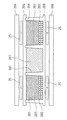
(方式1)
図11は、特表2001−500172号公報などにも記載されている本方式1の構成を示している。すなわち、マイクロカプセル100に、反対の電荷を帯電した黒色粒子101及び白色粒子102を、透明流動液103と共に封止し、このマイクロカプセル100を電極104で上下から挟み込み、さらに制御用の回路や配線(図示省略)が形成された基板105,105で上下から挟み込んだ構造としている。基板105は、電子ペーパー全体を支える役目も果たしている。また、図11は、黒色粒子101に負の電荷を、白色粒子102に正の電荷を帯電した場合を示している。電極104を介して電界を印加することにより、黒色及び白色の荷電粒子を反対方向に移動させることによって、表示を黒または白に切り替えることが可能になっている。なお、マイクロカプセル100は、厚さをほぼ均一に敷き詰めて使う必要があるため、樹脂膜106の上に並べた上で、接着材107によりマイクロカプセル100と樹脂膜106とが接着されている。以下の説明では、マイクロカプセル100と樹脂膜106と接着剤107をまとめて、マイクロカプセルシート100Sと呼ぶことにする。
(Method 1)
FIG. 11 shows the configuration of the present system 1, which is also described in JP-T-2001-500192. That is,
また、図11では、1つのマイクロカプセル100に対して、その上部基板105側に2個の電極104,104を配置し、下部基板105側に2個の電極104,104を配置している。すなわち、これら4個の電極で1つのマイクロカプセル100の黒色粒子101及び白色粒子102の移動を制御するようになっている。
In FIG. 11, two
例えば、図11の左端のマイクロカプセル100に着目すると、このマイクロカプセル100に対応する上部側の2個の電極104,104が共に負極性に印加され、下部側の2個の電極104,104が共に正極性に印加されている。そのため、白色粒子102が全て上部に移動し、黒色粒子101が全て下部に移動している。
For example, when attention is paid to the
また、図11の右端のマイクロカプセル100に着目すると、このマイクロカプセル100に対応する上部側の2個の電極104,104が共に正極性に印加され、下部側の2個の電極104,104が共に負極性に印加されている。そのため、白色粒子102が全て下部に移動し、黒色粒子101が全て上部に移動している。
When attention is paid to the
また、図11の中央部のマイクロカプセル100に着目すると、このマイクロカプセル100に対応する上部側の2個の電極104,104のうち、左側の電極104が負極性に印加され、右側の電極104が正極性に印加されている。一方、下部側の2個の電極104,104のうち、左側の電極104が正極性に印加され、右側の電極104が負極性に印加されている。そのため、白色粒子102の半分が、上部左側の電極104に引き付けられてマイクロカプセル100内を上部左側に移動し、黒色粒子101の半分が、上部右側の電極104に引き付けられてマイクロカプセル100内を上部右側に移動している。また、白色粒子102の残り半分が、下部右側の電極104に引き付けられてマイクロカプセル100内を下部右側に移動し、黒色粒子101の残り半分が、下部左側の電極104に引き付けられてマイクロカプセル100内を下部左側に移動している。
When attention is paid to the
(方式2)
図12は、特表2003−526817号公報などにも記載されている本方式2の構成を示している。すなわち、平板状の樹脂200に一定の間隔で隣接するようにエンボス(くぼみ)201を作り、そのくぼみ201の中に、帯電させた白色粒子202と着色流動液203を内包し、封止層204で蓋をした状態で、電極205により上下から挟み込み、さらに制御用の回路や配線(図示省略)が形成された基板206,206で上下から挟み込んだ構造としている。基板206は、電子ペーパー全体を支える役目も果たしている。図12では、白色粒子202を負に帯電させた場合を示している。電極205を介して電界を印加することにより、白色粒子202を移動させることによって、表示を白または流動液色に切り替えることが可能になっている。
(Method 2)
FIG. 12 shows the configuration of the method 2 described in Japanese Patent Application Publication No. 2003-526817. That is, an emboss (indentation) 201 is formed so as to be adjacent to the
(方式3)
図13は、特開2004−184620号公報などにも記載されている本方式3の構成を示している。すなわち、上下に対向配置された一対の電極305,305を前後左右方向に所定の隙間を存して配置し、その前後左右の隙間部分にそれぞれ隔壁301を配置することで、電極305と隔壁301とによって区切られた複数の小部屋306を形成し、それぞれの小部屋306内に、反対の電荷を帯電した黒色粒子302及び白色粒子303を空気304と共に封止した構造としている。図中の符号307は電子ペーパー全体を支えている基板であり、図示は省略しているが制御用の回路や配線が形成されている。電極305を介して小部屋306内に電界を印加することにより、黒色粒子302及び白色粒子303を反対方向に移動させることによって、表示を黒または白に切り替えることが可能になっている。
(Method 3)
FIG. 13 shows a configuration of the present system 3, which is also described in Japanese Patent Application Laid-Open No. 2004-184620. In other words, a pair of
上記いずれの方式の場合も、そのままでの状態でパンチ穴あけやホッチキス止めを行うと、封止が破られ、封止されていた荷電粒子や流動液が漏れ出す可能性がある。なお、以下の説明では、これらの荷電粒子や流動液などの電子インク材料を単にインクと総称する。パンチ穴あけやホッチキス止めに伴うインクの漏れを防止するためには、穴あけやホッチキス止めの対象領域内にインクを封止していなければ良い。従って、本発明の電子ペーパーでは、穴あけやホッチキス止めの作業領域内にインクを封止しない構造としている。 In any of the above methods, if punch punching or stapling is performed in the state as it is, the sealing is broken, and the charged particles and the fluid that has been sealed may leak out. In the following description, electronic ink materials such as charged particles and fluids are simply referred to as ink. In order to prevent ink leakage associated with punching and staples, it is sufficient that the ink is not sealed in the target area for punching and staples. Therefore, the electronic paper according to the present invention has a structure in which ink is not sealed in the work area for punching and stapling.
<本発明の実施形態に係る電子ペーパーの説明>
以下、本発明の実施形態に係る電子ペーパーについて説明する。
<Description of Electronic Paper According to Embodiment of the Present Invention>
Hereinafter, electronic paper according to an embodiment of the present invention will be described.
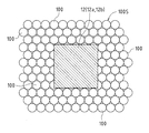
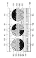
本実施形態の電子ペーパー1は、図1に示すように、表示領域11内に穴あけ用またはホッチキス止め用の作業領域12(12a,12b)を設け、制御用の回路及び配線はこの作業領域12を回避させて配置している。また、この作業領域12内は表示用のインクを封止しない構造としている。これにより、表示領域11を広くとっても、穴あけやホッチキス止めにより、インク漏れや動作不良を生じることのない電子ペーパーを実現することができる。
As shown in FIG. 1, the electronic paper 1 according to the present embodiment is provided with a work area 12 (12a, 12b) for punching or stapling in a
ここで、ホッチキス止め用の作業領域12aは、矩形形状の表示領域11の各角隅部の4箇所またはそれらのうちの一部箇所に設けることが好ましい。本実施形態では、各角隅部の4箇所全てに作業領域12aを設けた例を示している。また、穴あけ用の作業領域12bは、矩形形状の表示領域11の上下左右の各辺11a,11b,11c,11d近傍または前記各辺の一部の近傍に設けることが好ましい。本実施形態では、上下左右の全ての辺の近傍に作業領域12bを設けた例を示している。作業領域12a,12bをこのように設けることで、表示領域11への表示が上下逆になっても、その表示方向に合わせた角隅部にホッチキス止め行うことができるとともに、その表示方向に合わせた辺側にファイリング用の穴をあけることができる。
Here, it is preferable to provide the
ここで、インクを封止しない作業領域12(12a,12b)を形成する方法について、上記3つの方式のそれぞれについて説明する。 Here, a method for forming the work area 12 (12a, 12b) that does not seal ink will be described for each of the three methods.
(方式1の場合の作業領域の形成方法)
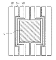
図11に示したマイクロカプセル100内に帯電粒子101,102と透明流動液103を封止した方式の場合、図2に一部拡大して示すように、マイクロカプセルシート100Sを電極104で挟み込む前に、パンチ穴あけやホッチキス止めのための作業領域12を予め切り取っておく。これにより、その後、電極104で上下から挟み込み、さらに基板105で挟み込んで電子ペーパー1を製造した後、作業領域12に穴をあけても、その部分にはインクが存在しないため、インクが漏れることはない。
(Method of forming work area in case of method 1)
In the case where the charged
(方式2の場合の作業領域の形成方法)
図12に示したエンボス201と封止層204を用いて帯電粒子202と着色流動液203を封止した方式の場合、図3に示すように、穴あけやホッチキス止めの作業領域12となる領域のエンボス201を、樹脂200と同じ材質の材料または樹脂200とは異なる材質の材料(図3中符号207により斜線を付して示している。)で埋めておくことにより、作業領域12にインクが封止されないようにすることができる。なお、図3では、1つのエンボス201にのみ樹脂207を埋めているが、作業領域12が周辺の複数のエンボスに跨がる場合には、当然、これらエンボス201にも樹脂207を埋めておく。これにより、この作業領域12に穴をあけても、インクが漏れることはない。なお、樹脂200と同じ材質の材料で埋める場合は、樹脂200にエンボス201を成型する際に穴あけの該当箇所だけエンボスを成型しないことで実現できるため、製造時の手順を増やすことなく対応することが可能である。一方、樹脂200とは異なる材質の材料で埋める場合は、樹脂200より柔らかい材質のものを用いることで、その後の穴あけ作業等を容易に行うことが可能になる。
(Method for forming work area in case of method 2)
In the case where the charged
(方法3の場合の作業領域の形成方法)
図13に示した電極305と隔壁301で区切られた小部屋306に、帯電粒子302,303と空気304を封止した方式の場合、図4に示すように、穴あけやホッチキス止めの作業領域12となる小部屋306を隔壁301と同じ材質の材料または隔壁301の材質とは異なる材質の材料(図4中符号308により斜線を付して示している。)で埋めておくことにより、作業領域12にインクが封止されないようにすることができる。なお、図4では、1つの小部屋306にのみ埋め込み材料308を埋めているが、作業領域12が周辺の複数の小部屋に跨がる場合には、当然、これら小部屋306にも埋め込み材料308を埋めておく。これにより、この作業領域12に穴をあけても、インクが漏れることはない。なお、隔壁301と同じ材質の材料で埋める場合は、隔壁301と一体で成型することができるため、製造時の手順を増やすことなく対応することが可能である。一方、隔壁301とは異なる材質の材料で埋める場合は、隔壁301の材質より柔らかい材質のものを用いることで、その後の穴あけ作業等を容易に行うことが可能となる。
(Method of forming work area in method 3)
In the case where the charged
次に、インク部分に外部電界を与える電極及び配線の配置構造について説明する。 Next, an arrangement structure of electrodes and wirings for applying an external electric field to the ink portion will be described.
電極の配置には、大きく分けると、表示したい形の電極を用意しておくセグメント配置と、小さい電極を規則正しく敷き詰めたマトリックス配置とがあるが、本実施形態では表示の自由度が高いマトリックス配置の場合について説明する。 The electrode arrangement can be roughly divided into a segment arrangement in which electrodes having a shape to be displayed are prepared and a matrix arrangement in which small electrodes are regularly arranged. In this embodiment, the matrix arrangement has a high degree of freedom in display. The case will be described.
マトリックス配置の場合、更にアクティブマトリックス方式と単純マトリックス方式に分けることができ、それぞれの場合について説明する。 The matrix arrangement can be further divided into an active matrix system and a simple matrix system, and each case will be described.
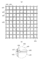
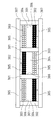
アクティブマトリックス方式の場合、図6に示すように、電極401の電位を制御するための配線が、縦横に交差して格子状に走っている。以下の説明では、縦方向の配線を列配線402、横方向の配線を行配線403と呼ぶことにする。なお、図6及び本実施形態に係わる図5では、列配線と行配線を共に太い実線で示している。図6(a)の右下の丸印404の部分を拡大した図を図6(b)に示している。同図(b)に示すように、電極401は、TFTトランジスタ406と枝配線407を介して、列配線402及び行配線403と接続されており、各々の電極401の電位を制御できるようになっている。図11から図13では、インク部分の上下に個別の電極が配置されているように示しているが、アクティブマトリックス方式では、電極401、列配線402、行配線403はインク部分の上方または下方のどちらか一方に存在し、反対側の電極は個別に別れている電極ではなく、一面のベタ電極の構造になっている。
In the case of the active matrix system, as shown in FIG. 6, wirings for controlling the potential of the
図6に示す配線状態では、穴あけを行うと、穴の位置405に該当する列配線402及び行配線403が切断され、穴の縦方向または横方向全ての電極の制御が不可能になる。また、ホッチキス止めを行う場合には、穴あけによる配線の切断のほか、ホッチキスの針を通じて、異なる行配線間、または異なる列配線間、または行配線と列配線間で短絡が起こり、正しく制御が行われない可能性もある。
In the wiring state shown in FIG. 6, when drilling is performed, the
これに対し、本実施形態では、図5に示すように、穴あけやホッチキス止めの対象となる作業領域12の配線は、予めその作業領域12を避けて(迂回するように)配線している。この際、作業領域12の周囲の電極401は取り除き、その場所を迂回配線のための領域として使用している。この領域は、穴あけやホッチキス止めの対象ではないが、電極401が存在せず表示には使用しないため、作業領域12だけでなくこの領域もインク材料の封止を止めても良い。
On the other hand, in this embodiment, as shown in FIG. 5, the wiring of the
単純マトリックス方式の場合、図9に示すように、帯形状の電極が、縦横に交差して格子状に配置されている。以下の説明では、縦方向の電極を列電極501、横方向の電極を行電極502と呼ぶことにする。なお、図9及び本実施形態に係わる図7と図8では、列配線と行配線を共に太い実線で示している。単純マトリックス方式では、インク部分を列電極と行電極で上下から挟み込む構造(どちらが上でも良い)になっており、特定の列電極と行電極に電位を印加することにより、交差部分503への印加電界を制御できるようになっている。
In the case of the simple matrix method, as shown in FIG. 9, the strip-shaped electrodes are arranged in a lattice pattern so as to intersect vertically and horizontally. In the following description, the vertical electrodes are referred to as
図9に示す電極配置では、穴あけを行うと、穴の位置504に該当する列電極501及び行電極502が切断され、穴の縦方向または横方向全ての交差部分503の電界制御すなわち表示制御が不可能になる。また、ホッチキス止めを行う場合には、ホッチキスの針を通じて、異なる行電極間、または異なる列電極間、または行電極と列電極間で短絡が起こり、正しく制御が行われない可能性もある。
In the electrode arrangement shown in FIG. 9, when drilling is performed, the
これに対し、本実施形態では、図7(列電極)及び図8(行電極)に示すように、穴あけやホッチキス止めの対象となる作業領域12の電極は、予めその作業領域12を避けた(迂回した)配置にしている。この際、作業領域12の周囲では、電極の幅が細く迂回した形になっており、この領域は通常の表示が行えないため、作業領域12だけでなくこの領域もインク材料の封止を止めても良い。
On the other hand, in this embodiment, as shown in FIG. 7 (column electrode) and FIG. 8 (row electrode), the electrode of the
このように、穴をあける可能性のある作業領域12にはインクを封止せず、かつ、配線を避けることにより、作業領域12に穴をあけた場合でも、インク漏れや動作不良が発生することはない。
In this way, ink is not sealed in the
ただし、インクをカプセル化するなど、穴があいた際のインク漏れの影響を極力おさえた構造になっている場合は、作業領域12へのインクの封止は行われていても構わない。
However, when the ink is encapsulated, or the like, the ink area is sealed in the
なお、図示は省略しているが、セグメント配置の場合も同様に、穴をあける可能性のある場所の配線をよけて配線する必要があるが、一般的にマトリックス配置と比べて配線密度が低いため、穴をあける可能性がある場所を避けて配線するのは容易である。 Although illustration is omitted, similarly in the case of the segment arrangement, it is necessary to avoid the wiring where there is a possibility of making a hole, but generally the wiring density is lower than that of the matrix arrangement. Because it is low, it is easy to route around where there is a possibility of drilling holes.
上記構成とすれば、穴をあける可能性のある作業領域12にはインクを封止せず、かつ、配線を避けることにより、作業領域12に穴をあけた場合でも、インク漏れや動作不良が発生することはない。しかし、それ以外の領域に間違って穴をあけてしまった場合には、インク漏れや動作不良を起こすことになる。従って、穴をあけて良い領域を電子ペーパーの使用者に明示する必要がある。
With the above configuration, ink is not sealed in the
そこで、本実施形態では、図1及び図10に示すように、作業領域12上に、作業領域であることを示す印13が付けられている。図10(a)は、パンチ穴をあけて良い場所を示す印(穴マーク)のパターン例であり、同図(b)は、ホッチキス止めをして良い場所を示す印(針マーク)のパターン例である。しかし、このようなパターンを目立つ色や濃さの印刷などで表示すると、本来の電子ペーパーの表示の邪魔になる可能性がある。そのため、本実施形態では、目立たない色でパターンを印刷する。具体的には、薄い青色や緑色で印刷する。この場合、見た目に目立たないだけでなく、白黒複写機でコピーを取った際にも、コピーにパターンの表示が移ることを低減できる。また、他の実施形態としては、電子ペーパー1の表面に凹凸を付けて(刻印して)、該当領域を表示する方法もある。
Therefore, in this embodiment, as shown in FIGS. 1 and 10, a
なお、上記実施形態では、電子ペーパー1の角隅部をホッチキス止め用、各辺部分を穴あけ用として、印13を区別して示しているが、このようにホッチキス止め用と穴あけ用とに区別する必要はない。すなわち、印13は、その図柄に関係なく、あくまで穴あけやホッチキス止めを行って良い場所を示しているに過ぎず、その印13の作業領域に穴をあけるか、ホッチキス止めを行うかは使用者の自由である。
In the above-described embodiment, the corners of the electronic paper 1 are used for staples, and the side portions are used for punching. The
また、上記実施形態では、作業領域12は、電子ペーパー1を使用する際の向きを制限しないように、図1に示すようにその全周に設けているが、電子ペーパー1を使用する向きが制限できるのであれば、その向きにあった箇所にのみ作業領域12を形成してもよい。これにより、表示領域をより広く確保することが可能となる。
Moreover, in the said embodiment, although the work area |
また、図1では、穴あけ用の作業領域12bを、パンチ穴向けの一辺に2箇所設けるように示しているが、これに限らずルーズリーフ用の綴じ穴のように、一辺にもっと多数の作業領域を設けても良い。
Further, in FIG. 1, the
また、穴あけは使用者が後から行うのではなく、電子ペーパーの製造過程で予め穴をあけておいても良い。製造過程で穴をあけておくことにより、穴あけ時に作業領域外に穴をあけてしまう失敗をなくすことができ、また、穴を正確な位置にあけられるため作業領域12bも必要最低限な大きさで良く、その分、電子ペーパーの表示可能な領域を大きくすることができる。
Moreover, the user does not perform the drilling later, but may perform the drilling in advance in the manufacturing process of the electronic paper. By making a hole in the manufacturing process, it is possible to eliminate the failure to make a hole outside the work area when drilling, and the
また、上記実施形態では、作業領域12a、12bの形状を正方形で図示しているが、正方形に限定するものではなく、任意の形状を取ることが可能である。
Moreover, in the said embodiment, although the shape of work area |
なお、本実施形態の電子ペーパーの大きさは、現状の紙と同じ定型サイズ(A4など)にすることにより、現状の紙と一緒に穴あけやホッチキス止めができ、既存のバインダーに綴じることもでき、収納も既存の定型サイズ用のものが使用でき、流通においても既存の紙と同じように扱え、既存のコピー機やスキャナにかけることができるなど、現状の紙と同等に扱うことができる。さらに、前記ホッチキス止め用または穴あけ用の作業領域を設ける位置は統一しておくことにより、複数の電子ペーパーや現状の紙をまとめてホッチキス止めやパンチ穴をあける際に、すべての電子ペーパーの作業領域の位置をいちいち確認しなくても、一枚の電子ペーパーの前記ホッチキス止め用または穴あけ用の作業領域の位置を確認するだけでホッチキス止めやパンチ穴をあける作業が可能であり、作業の効率を上げることができる。特に、電子ペーパーや従来の紙を重ねた際に一番上が電子ペーパーの場合は、その一番上の電子ペーパーの作業領域を確認するだけで、ホッチキス止めやパンチ穴あけの作業ができるため、従来の紙だけをホッチキス止めやパンチ穴あけするのと、ほとんど作業効率が変わらなくすることが可能である。 The size of the electronic paper of the present embodiment is the same standard size (A4, etc.) as the current paper, so that it can be punched and stapled together with the current paper, and can be bound to an existing binder. In addition, storage for existing standard sizes can be used, and it can be handled in the same way as existing paper in distribution, and can be handled in the same way as current paper, such as being able to be loaded on an existing copier or scanner. In addition, by unifying the position where the stapler or punching work area is provided, all electronic papers can be worked on when punching holes or punching holes together. Without checking the position of each area, it is possible to work on staples and punch holes just by checking the position of the staple or punching work area of a piece of electronic paper. Can be raised. In particular, when electronic paper or conventional paper is stacked, if the top is electronic paper, just check the work area of the top electronic paper, so you can staple and punch holes. It is possible to make the work efficiency almost the same as when stapled or punched with only conventional paper.
1 電子ペーパー
11 表示領域
12(12a,12b) 作業領域
13 印
100 マイクロカプセル
100S マイクロカプセルシート
101 黒色粒子
102 白色粒子
103 透明流動液
104 電極
105 基板
106 樹脂膜
107 接着剤
200 樹脂
201 エンボス(くぼみ)
202 白色粒子
203 着色流動液
204 封止層
205 電極
206 基板
207 樹脂
301 隔壁
302 黒色粒子
303 白色粒子
304 空気
305 電極
306 小部屋
307 基板
401 電極
402 列配線
403 行配線
406 TFTトランジスタ
501 列電極
502 行電極
DESCRIPTION OF SYMBOLS 1
202
Claims (16)
前記作業領域内は表示用の電子インク材料を封止しないことを特徴とする電子ペーパー。 The electronic paper according to claim 1,
Electronic paper characterized by not sealing display electronic ink material in the work area.
前記ホッチキス止め用の作業領域は、矩形形状の前記表示領域の各角隅部の4箇所または前記4箇所のうちの一部箇所に設けられていることを特徴とする電子ペーパー。 In the electronic paper according to claim 1 or 2,
The stapler-stopping work area is provided at four corners of the rectangular display area or at a part of the four places.
前記穴あけ用の作業領域は、矩形形状の前記表示領域の各辺近傍または前記各辺のうちの一部の近傍に設けられていることを特徴とする電子ペーパー。 In the electronic paper according to claim 1 or 2,
The electronic paper, wherein the work area for drilling is provided in the vicinity of each side of the rectangular display area or in the vicinity of a part of the sides.
前記穴あけ用の作業領域に、予め穴があけられていることを特徴とする電子ペーパー。 The electronic paper according to claim 4,
An electronic paper, wherein a hole is previously drilled in the drilling work area.
前記作業領域上には当該作業領域の場所を示す印が付けられていることを特徴とする電子ペーパー。 In the electronic paper according to claim 1 or 2,
An electronic paper, wherein a mark indicating the location of the work area is marked on the work area.
前記印は目立たない色で印刷されていることを特徴とする電子ペーパー。 The electronic paper according to claim 6,
The electronic paper is characterized in that the mark is printed in an inconspicuous color.
前記印は前記作業領域の表面に凹凸を付けることで設けられていることを特徴とする電子ペーパー。 The electronic paper according to claim 6,
The electronic paper is characterized in that the mark is provided by making irregularities on the surface of the work area.
前記作業領域上には当該作業領域の場所を示す印が付けられていることを特徴とする電子ペーパー。 The electronic paper according to claim 3,
An electronic paper, wherein a mark indicating the location of the work area is marked on the work area.
前記印は目立たない色で印刷されていることを特徴とする電子ペーパー。 The electronic paper according to claim 9, wherein
The electronic paper is characterized in that the mark is printed in an inconspicuous color.
前記印は前記作業領域の表面に凹凸を付けることで設けられていることを特徴とする電子ペーパー。 The electronic paper according to claim 9, wherein
The electronic paper is characterized in that the mark is provided by making irregularities on the surface of the work area.
前記作業領域上には当該作業領域の場所を示す印が付けられていることを特徴とする電子ペーパー。 The electronic paper according to claim 4,
An electronic paper, wherein a mark indicating the location of the work area is marked on the work area.
前記印は目立たない色で印刷されていることを特徴とする電子ペーパー。 The electronic paper according to claim 12,
The electronic paper is characterized in that the mark is printed in an inconspicuous color.
前記印は前記作業領域の表面に凹凸を付けることで設けられていることを特徴とする電子ペーパー。 The electronic paper according to claim 12,
The electronic paper is characterized in that the mark is provided by making irregularities on the surface of the work area.
前記電子ペーパーの大きさを従来の紙の定型サイズに合せることを特徴とする電子ペーパー。 In the electronic paper according to claim 1 or 2,
An electronic paper characterized in that the size of the electronic paper is matched to the standard size of conventional paper.
前記穴あけ用またはホッチキス止め用の作業領域を決まった位置に設けることを特徴とする電子ペーパー。 The electronic paper according to claim 15,
An electronic paper characterized in that a work area for punching or stapling is provided at a fixed position.
Priority Applications (1)
| Application Number | Priority Date | Filing Date | Title |
|---|---|---|---|
| JP2008167700A JP5052427B2 (en) | 2008-06-26 | 2008-06-26 | Electronic paper |
Applications Claiming Priority (1)
| Application Number | Priority Date | Filing Date | Title |
|---|---|---|---|
| JP2008167700A JP5052427B2 (en) | 2008-06-26 | 2008-06-26 | Electronic paper |
Publications (2)
| Publication Number | Publication Date |
|---|---|
| JP2010008698A true JP2010008698A (en) | 2010-01-14 |
| JP5052427B2 JP5052427B2 (en) | 2012-10-17 |
Family
ID=41589290
Family Applications (1)
| Application Number | Title | Priority Date | Filing Date |
|---|---|---|---|
| JP2008167700A Expired - Fee Related JP5052427B2 (en) | 2008-06-26 | 2008-06-26 | Electronic paper |
Country Status (1)
| Country | Link |
|---|---|
| JP (1) | JP5052427B2 (en) |
Cited By (1)
| Publication number | Priority date | Publication date | Assignee | Title |
|---|---|---|---|---|
| JP2014134766A (en) * | 2013-01-11 | 2014-07-24 | Au Optronics Corp | Display panel and display device |
Citations (4)
| Publication number | Priority date | Publication date | Assignee | Title |
|---|---|---|---|---|
| JP2003167271A (en) * | 2001-11-30 | 2003-06-13 | Optrex Corp | Liquid crystal display element |
| JP2006074311A (en) * | 2004-09-01 | 2006-03-16 | Fuji Xerox Co Ltd | Electronic paper |
| JP2006091226A (en) * | 2004-09-22 | 2006-04-06 | Fuji Xerox Co Ltd | Electronic paper |
| JP2008058906A (en) * | 2006-09-04 | 2008-03-13 | Bridgestone Corp | Panel for information display |
-
2008
- 2008-06-26 JP JP2008167700A patent/JP5052427B2/en not_active Expired - Fee Related
Patent Citations (4)
| Publication number | Priority date | Publication date | Assignee | Title |
|---|---|---|---|---|
| JP2003167271A (en) * | 2001-11-30 | 2003-06-13 | Optrex Corp | Liquid crystal display element |
| JP2006074311A (en) * | 2004-09-01 | 2006-03-16 | Fuji Xerox Co Ltd | Electronic paper |
| JP2006091226A (en) * | 2004-09-22 | 2006-04-06 | Fuji Xerox Co Ltd | Electronic paper |
| JP2008058906A (en) * | 2006-09-04 | 2008-03-13 | Bridgestone Corp | Panel for information display |
Cited By (1)
| Publication number | Priority date | Publication date | Assignee | Title |
|---|---|---|---|---|
| JP2014134766A (en) * | 2013-01-11 | 2014-07-24 | Au Optronics Corp | Display panel and display device |
Also Published As
| Publication number | Publication date |
|---|---|
| JP5052427B2 (en) | 2012-10-17 |
Similar Documents
| Publication | Publication Date | Title |
|---|---|---|
| JP5955298B2 (en) | Display panel and display device | |
| JP4992967B2 (en) | Display panel, multilayer display element and manufacturing method thereof | |
| EP1939677A1 (en) | Electrophoretic display medium and its formation method | |
| JP2009536430A5 (en) | ||
| JP4701616B2 (en) | Electronic notebook, electronic notebook display medium | |
| TW200617479A (en) | Liquid crystal display device | |
| CN102369479B (en) | Electronic paper and method for producing same | |
| JP5052427B2 (en) | Electronic paper | |
| CN107783334A (en) | Array base palte, display panel and electronic equipment | |
| TWI457884B (en) | Flexible liquid crystal display and flexible fluid display | |
| CN106488664A (en) | Flexible printed circuit film and the display device using this flexible printed circuit film | |
| CN104698691B (en) | Liquid crystal display and its manufacturing method | |
| CN107340661A (en) | Array base palte, display panel and electronic equipment | |
| JP4685077B2 (en) | Mobile phone equipment | |
| JP2009003151A (en) | Flat panel display and manufacturing method therefor | |
| US20120044450A1 (en) | Liquid crystal display apparatus and method for manufacturing the same | |
| KR20160081999A (en) | Liquid Crystal Display Device | |
| JP3861656B2 (en) | Toner container | |
| CN104267545B (en) | Display device | |
| JP2013222088A (en) | Base material for electrophoretic display device and manufacturing method for the same, and electrophoretic display device and manufacturing method for the same | |
| CN106842410B (en) | Backlight module and display device | |
| JP2007256385A (en) | Optical sheet unit | |
| WO2007111063A1 (en) | Liquid crystal display apparatus and process for manufacturing the same | |
| CN104987842B (en) | Adhesive tape manufacturing equipment | |
| JP4631988B2 (en) | Circuit board |
Legal Events
| Date | Code | Title | Description |
|---|---|---|---|
| A621 | Written request for application examination |
Free format text: JAPANESE INTERMEDIATE CODE: A621 Effective date: 20100826 |
|
| A977 | Report on retrieval |
Free format text: JAPANESE INTERMEDIATE CODE: A971007 Effective date: 20120216 |
|
| A131 | Notification of reasons for refusal |
Free format text: JAPANESE INTERMEDIATE CODE: A131 Effective date: 20120221 |
|
| A521 | Written amendment |
Free format text: JAPANESE INTERMEDIATE CODE: A523 Effective date: 20120419 |
|
| RD02 | Notification of acceptance of power of attorney |
Free format text: JAPANESE INTERMEDIATE CODE: A7422 Effective date: 20120419 |
|
| TRDD | Decision of grant or rejection written | ||
| A01 | Written decision to grant a patent or to grant a registration (utility model) |
Free format text: JAPANESE INTERMEDIATE CODE: A01 Effective date: 20120703 |
|
| A01 | Written decision to grant a patent or to grant a registration (utility model) |
Free format text: JAPANESE INTERMEDIATE CODE: A01 |
|
| A61 | First payment of annual fees (during grant procedure) |
Free format text: JAPANESE INTERMEDIATE CODE: A61 Effective date: 20120724 |
|
| R150 | Certificate of patent or registration of utility model |
Free format text: JAPANESE INTERMEDIATE CODE: R150 |
|
| FPAY | Renewal fee payment (event date is renewal date of database) |
Free format text: PAYMENT UNTIL: 20150803 Year of fee payment: 3 |
|
| LAPS | Cancellation because of no payment of annual fees |